JP4834228B2 - Method of manufacturing a trench semiconductor device with a gate oxide layer having a plurality of thicknesses - Google Patents
Method of manufacturing a trench semiconductor device with a gate oxide layer having a plurality of thicknesses Download PDFInfo
- Publication number
- JP4834228B2 JP4834228B2 JP2000620671A JP2000620671A JP4834228B2 JP 4834228 B2 JP4834228 B2 JP 4834228B2 JP 2000620671 A JP2000620671 A JP 2000620671A JP 2000620671 A JP2000620671 A JP 2000620671A JP 4834228 B2 JP4834228 B2 JP 4834228B2
- Authority
- JP
- Japan
- Prior art keywords
- trench
- layer
- oxide
- polysilicon
- semiconductor material
- Prior art date
- Legal status (The legal status is an assumption and is not a legal conclusion. Google has not performed a legal analysis and makes no representation as to the accuracy of the status listed.)
- Expired - Fee Related
Links
- 239000004065 semiconductor Substances 0.000 title claims abstract description 70
- 238000004519 manufacturing process Methods 0.000 title claims abstract description 47
- 238000000034 method Methods 0.000 claims abstract description 218
- 230000008569 process Effects 0.000 claims abstract description 177
- 229910021420 polycrystalline silicon Inorganic materials 0.000 claims abstract description 176
- 229920005591 polysilicon Polymers 0.000 claims abstract description 176
- 239000000463 material Substances 0.000 claims abstract description 76
- 238000000151 deposition Methods 0.000 claims abstract description 56
- 238000005530 etching Methods 0.000 claims abstract description 47
- XUIMIQQOPSSXEZ-UHFFFAOYSA-N Silicon Chemical compound [Si] XUIMIQQOPSSXEZ-UHFFFAOYSA-N 0.000 claims abstract description 18
- 229910052710 silicon Inorganic materials 0.000 claims abstract description 18
- 239000010703 silicon Substances 0.000 claims abstract description 18
- 238000006243 chemical reaction Methods 0.000 claims abstract description 11
- 238000010438 heat treatment Methods 0.000 claims abstract description 5
- 230000005684 electric field Effects 0.000 claims description 45
- 230000008021 deposition Effects 0.000 claims description 36
- 150000004767 nitrides Chemical class 0.000 claims description 35
- 229920002120 photoresistant polymer Polymers 0.000 claims description 21
- 230000003647 oxidation Effects 0.000 claims description 17
- 238000007254 oxidation reaction Methods 0.000 claims description 17
- 125000006850 spacer group Chemical group 0.000 claims description 15
- 239000004020 conductor Substances 0.000 claims description 14
- 230000001590 oxidative effect Effects 0.000 claims description 7
- 229910052581 Si3N4 Inorganic materials 0.000 claims description 6
- HQVNEWCFYHHQES-UHFFFAOYSA-N silicon nitride Chemical compound N12[Si]34N5[Si]62N3[Si]51N64 HQVNEWCFYHHQES-UHFFFAOYSA-N 0.000 claims description 6
- 239000002253 acid Substances 0.000 claims description 3
- 239000002245 particle Substances 0.000 claims 9
- 239000010410 layer Substances 0.000 description 361
- 230000015556 catabolic process Effects 0.000 description 19
- 229910052751 metal Inorganic materials 0.000 description 15
- 239000002184 metal Substances 0.000 description 15
- 238000010586 diagram Methods 0.000 description 10
- 239000011521 glass Substances 0.000 description 10
- 239000000758 substrate Substances 0.000 description 10
- 230000000694 effects Effects 0.000 description 9
- 230000006870 function Effects 0.000 description 9
- 150000002500 ions Chemical class 0.000 description 8
- 210000000746 body region Anatomy 0.000 description 7
- 239000003989 dielectric material Substances 0.000 description 7
- 230000000873 masking effect Effects 0.000 description 7
- QVGXLLKOCUKJST-UHFFFAOYSA-N atomic oxygen Chemical compound [O] QVGXLLKOCUKJST-UHFFFAOYSA-N 0.000 description 5
- 239000001301 oxygen Substances 0.000 description 5
- 229910052760 oxygen Inorganic materials 0.000 description 5
- 238000005229 chemical vapour deposition Methods 0.000 description 4
- 230000008878 coupling Effects 0.000 description 4
- 238000010168 coupling process Methods 0.000 description 4
- 238000005859 coupling reaction Methods 0.000 description 4
- 229920000642 polymer Polymers 0.000 description 4
- 230000015572 biosynthetic process Effects 0.000 description 3
- 239000002019 doping agent Substances 0.000 description 3
- BHEPBYXIRTUNPN-UHFFFAOYSA-N hydridophosphorus(.) (triplet) Chemical compound [PH] BHEPBYXIRTUNPN-UHFFFAOYSA-N 0.000 description 3
- 238000004544 sputter deposition Methods 0.000 description 3
- 239000000126 substance Substances 0.000 description 3
- IJGRMHOSHXDMSA-UHFFFAOYSA-N Atomic nitrogen Chemical compound N#N IJGRMHOSHXDMSA-UHFFFAOYSA-N 0.000 description 2
- 239000004642 Polyimide Substances 0.000 description 2
- BLRPTPMANUNPDV-UHFFFAOYSA-N Silane Chemical compound [SiH4] BLRPTPMANUNPDV-UHFFFAOYSA-N 0.000 description 2
- VYPSYNLAJGMNEJ-UHFFFAOYSA-N Silicium dioxide Chemical compound O=[Si]=O VYPSYNLAJGMNEJ-UHFFFAOYSA-N 0.000 description 2
- 125000004429 atom Chemical group 0.000 description 2
- 239000000969 carrier Substances 0.000 description 2
- 238000010276 construction Methods 0.000 description 2
- 230000005669 field effect Effects 0.000 description 2
- 239000001257 hydrogen Substances 0.000 description 2
- 229910052739 hydrogen Inorganic materials 0.000 description 2
- 238000002513 implantation Methods 0.000 description 2
- 230000007246 mechanism Effects 0.000 description 2
- 230000003071 parasitic effect Effects 0.000 description 2
- 238000005268 plasma chemical vapour deposition Methods 0.000 description 2
- 229920001721 polyimide Polymers 0.000 description 2
- 230000009467 reduction Effects 0.000 description 2
- 229920006395 saturated elastomer Polymers 0.000 description 2
- 229910000077 silane Inorganic materials 0.000 description 2
- VXEGSRKPIUDPQT-UHFFFAOYSA-N 4-[4-(4-methoxyphenyl)piperazin-1-yl]aniline Chemical compound C1=CC(OC)=CC=C1N1CCN(C=2C=CC(N)=CC=2)CC1 VXEGSRKPIUDPQT-UHFFFAOYSA-N 0.000 description 1
- ZOXJGFHDIHLPTG-UHFFFAOYSA-N Boron Chemical compound [B] ZOXJGFHDIHLPTG-UHFFFAOYSA-N 0.000 description 1
- 241000293849 Cordylanthus Species 0.000 description 1
- UFHFLCQGNIYNRP-UHFFFAOYSA-N Hydrogen Chemical compound [H][H] UFHFLCQGNIYNRP-UHFFFAOYSA-N 0.000 description 1
- ATJFFYVFTNAWJD-UHFFFAOYSA-N Tin Chemical compound [Sn] ATJFFYVFTNAWJD-UHFFFAOYSA-N 0.000 description 1
- 238000009825 accumulation Methods 0.000 description 1
- 229910052785 arsenic Inorganic materials 0.000 description 1
- RQNWIZPPADIBDY-UHFFFAOYSA-N arsenic atom Chemical compound [As] RQNWIZPPADIBDY-UHFFFAOYSA-N 0.000 description 1
- 230000004888 barrier function Effects 0.000 description 1
- 230000009286 beneficial effect Effects 0.000 description 1
- KGBXLFKZBHKPEV-UHFFFAOYSA-N boric acid Chemical compound OB(O)O KGBXLFKZBHKPEV-UHFFFAOYSA-N 0.000 description 1
- 239000004327 boric acid Substances 0.000 description 1
- 229910052796 boron Inorganic materials 0.000 description 1
- 239000006227 byproduct Substances 0.000 description 1
- 239000003990 capacitor Substances 0.000 description 1
- 230000008859 change Effects 0.000 description 1
- 239000002800 charge carrier Substances 0.000 description 1
- 239000013078 crystal Substances 0.000 description 1
- 230000007423 decrease Effects 0.000 description 1
- 230000007547 defect Effects 0.000 description 1
- 230000001066 destructive effect Effects 0.000 description 1
- MROCJMGDEKINLD-UHFFFAOYSA-N dichlorosilane Chemical compound Cl[SiH2]Cl MROCJMGDEKINLD-UHFFFAOYSA-N 0.000 description 1
- 238000009792 diffusion process Methods 0.000 description 1
- 238000009826 distribution Methods 0.000 description 1
- 238000005516 engineering process Methods 0.000 description 1
- 230000002708 enhancing effect Effects 0.000 description 1
- 238000007429 general method Methods 0.000 description 1
- 125000004435 hydrogen atom Chemical class [H]* 0.000 description 1
- 238000007654 immersion Methods 0.000 description 1
- 239000004615 ingredient Substances 0.000 description 1
- 238000009413 insulation Methods 0.000 description 1
- 230000003993 interaction Effects 0.000 description 1
- 238000000752 ionisation method Methods 0.000 description 1
- 230000007257 malfunction Effects 0.000 description 1
- 230000004048 modification Effects 0.000 description 1
- 238000012986 modification Methods 0.000 description 1
- 230000007935 neutral effect Effects 0.000 description 1
- 229910052757 nitrogen Inorganic materials 0.000 description 1
- 230000000737 periodic effect Effects 0.000 description 1
- 238000001020 plasma etching Methods 0.000 description 1
- 238000000623 plasma-assisted chemical vapour deposition Methods 0.000 description 1
- 238000012545 processing Methods 0.000 description 1
- 239000000047 product Substances 0.000 description 1
- 230000001737 promoting effect Effects 0.000 description 1
- 230000002040 relaxant effect Effects 0.000 description 1
- 230000002441 reversible effect Effects 0.000 description 1
- 230000000630 rising effect Effects 0.000 description 1
- 235000012239 silicon dioxide Nutrition 0.000 description 1
- 239000000377 silicon dioxide Substances 0.000 description 1
- 239000005049 silicon tetrachloride Substances 0.000 description 1
- 239000002356 single layer Substances 0.000 description 1
- 238000010301 surface-oxidation reaction Methods 0.000 description 1
- 230000008719 thickening Effects 0.000 description 1
- WFKWXMTUELFFGS-UHFFFAOYSA-N tungsten Chemical compound [W] WFKWXMTUELFFGS-UHFFFAOYSA-N 0.000 description 1
- 229910052721 tungsten Inorganic materials 0.000 description 1
- 239000010937 tungsten Substances 0.000 description 1
- XLYOFNOQVPJJNP-UHFFFAOYSA-N water Chemical compound O XLYOFNOQVPJJNP-UHFFFAOYSA-N 0.000 description 1
Images


Classifications
-
- H—ELECTRICITY
- H01—ELECTRIC ELEMENTS
- H01L—SEMICONDUCTOR DEVICES NOT COVERED BY CLASS H10
- H01L21/00—Processes or apparatus adapted for the manufacture or treatment of semiconductor or solid state devices or of parts thereof
- H01L21/70—Manufacture or treatment of devices consisting of a plurality of solid state components formed in or on a common substrate or of parts thereof; Manufacture of integrated circuit devices or of parts thereof
- H01L21/71—Manufacture of specific parts of devices defined in group H01L21/70
- H01L21/76—Making of isolation regions between components
- H01L21/762—Dielectric regions, e.g. EPIC dielectric isolation, LOCOS; Trench refilling techniques, SOI technology, use of channel stoppers
-
- H—ELECTRICITY
- H01—ELECTRIC ELEMENTS
- H01L—SEMICONDUCTOR DEVICES NOT COVERED BY CLASS H10
- H01L29/00—Semiconductor devices specially adapted for rectifying, amplifying, oscillating or switching and having potential barriers; Capacitors or resistors having potential barriers, e.g. a PN-junction depletion layer or carrier concentration layer; Details of semiconductor bodies or of electrodes thereof ; Multistep manufacturing processes therefor
- H01L29/66—Types of semiconductor device ; Multistep manufacturing processes therefor
- H01L29/68—Types of semiconductor device ; Multistep manufacturing processes therefor controllable by only the electric current supplied, or only the electric potential applied, to an electrode which does not carry the current to be rectified, amplified or switched
- H01L29/76—Unipolar devices, e.g. field effect transistors
- H01L29/772—Field effect transistors
- H01L29/78—Field effect transistors with field effect produced by an insulated gate
- H01L29/7801—DMOS transistors, i.e. MISFETs with a channel accommodating body or base region adjoining a drain drift region
- H01L29/7802—Vertical DMOS transistors, i.e. VDMOS transistors
- H01L29/7813—Vertical DMOS transistors, i.e. VDMOS transistors with trench gate electrode, e.g. UMOS transistors
-
- H—ELECTRICITY
- H01—ELECTRIC ELEMENTS
- H01L—SEMICONDUCTOR DEVICES NOT COVERED BY CLASS H10
- H01L29/00—Semiconductor devices specially adapted for rectifying, amplifying, oscillating or switching and having potential barriers; Capacitors or resistors having potential barriers, e.g. a PN-junction depletion layer or carrier concentration layer; Details of semiconductor bodies or of electrodes thereof ; Multistep manufacturing processes therefor
- H01L29/02—Semiconductor bodies ; Multistep manufacturing processes therefor
- H01L29/06—Semiconductor bodies ; Multistep manufacturing processes therefor characterised by their shape; characterised by the shapes, relative sizes, or dispositions of the semiconductor regions ; characterised by the concentration or distribution of impurities within semiconductor regions
- H01L29/08—Semiconductor bodies ; Multistep manufacturing processes therefor characterised by their shape; characterised by the shapes, relative sizes, or dispositions of the semiconductor regions ; characterised by the concentration or distribution of impurities within semiconductor regions with semiconductor regions connected to an electrode carrying current to be rectified, amplified or switched and such electrode being part of a semiconductor device which comprises three or more electrodes
- H01L29/0843—Source or drain regions of field-effect devices
- H01L29/0847—Source or drain regions of field-effect devices of field-effect transistors with insulated gate
- H01L29/0852—Source or drain regions of field-effect devices of field-effect transistors with insulated gate of DMOS transistors
- H01L29/0873—Drain regions
- H01L29/0878—Impurity concentration or distribution
-
- H—ELECTRICITY
- H01—ELECTRIC ELEMENTS
- H01L—SEMICONDUCTOR DEVICES NOT COVERED BY CLASS H10
- H01L29/00—Semiconductor devices specially adapted for rectifying, amplifying, oscillating or switching and having potential barriers; Capacitors or resistors having potential barriers, e.g. a PN-junction depletion layer or carrier concentration layer; Details of semiconductor bodies or of electrodes thereof ; Multistep manufacturing processes therefor
- H01L29/40—Electrodes ; Multistep manufacturing processes therefor
- H01L29/41—Electrodes ; Multistep manufacturing processes therefor characterised by their shape, relative sizes or dispositions
- H01L29/423—Electrodes ; Multistep manufacturing processes therefor characterised by their shape, relative sizes or dispositions not carrying the current to be rectified, amplified or switched
- H01L29/42312—Gate electrodes for field effect devices
- H01L29/42316—Gate electrodes for field effect devices for field-effect transistors
- H01L29/4232—Gate electrodes for field effect devices for field-effect transistors with insulated gate
- H01L29/42364—Gate electrodes for field effect devices for field-effect transistors with insulated gate characterised by the insulating layer, e.g. thickness or uniformity
- H01L29/42368—Gate electrodes for field effect devices for field-effect transistors with insulated gate characterised by the insulating layer, e.g. thickness or uniformity the thickness being non-uniform
-
- H—ELECTRICITY
- H01—ELECTRIC ELEMENTS
- H01L—SEMICONDUCTOR DEVICES NOT COVERED BY CLASS H10
- H01L29/00—Semiconductor devices specially adapted for rectifying, amplifying, oscillating or switching and having potential barriers; Capacitors or resistors having potential barriers, e.g. a PN-junction depletion layer or carrier concentration layer; Details of semiconductor bodies or of electrodes thereof ; Multistep manufacturing processes therefor
- H01L29/66—Types of semiconductor device ; Multistep manufacturing processes therefor
- H01L29/66007—Multistep manufacturing processes
- H01L29/66075—Multistep manufacturing processes of devices having semiconductor bodies comprising group 14 or group 13/15 materials
- H01L29/66227—Multistep manufacturing processes of devices having semiconductor bodies comprising group 14 or group 13/15 materials the devices being controllable only by the electric current supplied or the electric potential applied, to an electrode which does not carry the current to be rectified, amplified or switched, e.g. three-terminal devices
- H01L29/66409—Unipolar field-effect transistors
- H01L29/66477—Unipolar field-effect transistors with an insulated gate, i.e. MISFET
- H01L29/66674—DMOS transistors, i.e. MISFETs with a channel accommodating body or base region adjoining a drain drift region
- H01L29/66712—Vertical DMOS transistors, i.e. VDMOS transistors
- H01L29/66734—Vertical DMOS transistors, i.e. VDMOS transistors with a step of recessing the gate electrode, e.g. to form a trench gate electrode
-
- H—ELECTRICITY
- H01—ELECTRIC ELEMENTS
- H01L—SEMICONDUCTOR DEVICES NOT COVERED BY CLASS H10
- H01L29/00—Semiconductor devices specially adapted for rectifying, amplifying, oscillating or switching and having potential barriers; Capacitors or resistors having potential barriers, e.g. a PN-junction depletion layer or carrier concentration layer; Details of semiconductor bodies or of electrodes thereof ; Multistep manufacturing processes therefor
- H01L29/66—Types of semiconductor device ; Multistep manufacturing processes therefor
- H01L29/68—Types of semiconductor device ; Multistep manufacturing processes therefor controllable by only the electric current supplied, or only the electric potential applied, to an electrode which does not carry the current to be rectified, amplified or switched
- H01L29/76—Unipolar devices, e.g. field effect transistors
- H01L29/772—Field effect transistors
- H01L29/78—Field effect transistors with field effect produced by an insulated gate
- H01L29/7801—DMOS transistors, i.e. MISFETs with a channel accommodating body or base region adjoining a drain drift region
- H01L29/7802—Vertical DMOS transistors, i.e. VDMOS transistors
- H01L29/7803—Vertical DMOS transistors, i.e. VDMOS transistors structurally associated with at least one other device
- H01L29/7808—Vertical DMOS transistors, i.e. VDMOS transistors structurally associated with at least one other device the other device being a breakdown diode, e.g. Zener diode
-
- H—ELECTRICITY
- H01—ELECTRIC ELEMENTS
- H01L—SEMICONDUCTOR DEVICES NOT COVERED BY CLASS H10
- H01L29/00—Semiconductor devices specially adapted for rectifying, amplifying, oscillating or switching and having potential barriers; Capacitors or resistors having potential barriers, e.g. a PN-junction depletion layer or carrier concentration layer; Details of semiconductor bodies or of electrodes thereof ; Multistep manufacturing processes therefor
- H01L29/66—Types of semiconductor device ; Multistep manufacturing processes therefor
- H01L29/68—Types of semiconductor device ; Multistep manufacturing processes therefor controllable by only the electric current supplied, or only the electric potential applied, to an electrode which does not carry the current to be rectified, amplified or switched
- H01L29/76—Unipolar devices, e.g. field effect transistors
- H01L29/772—Field effect transistors
- H01L29/78—Field effect transistors with field effect produced by an insulated gate
- H01L29/7801—DMOS transistors, i.e. MISFETs with a channel accommodating body or base region adjoining a drain drift region
- H01L29/7802—Vertical DMOS transistors, i.e. VDMOS transistors
- H01L29/7811—Vertical DMOS transistors, i.e. VDMOS transistors with an edge termination structure
-
- H—ELECTRICITY
- H01—ELECTRIC ELEMENTS
- H01L—SEMICONDUCTOR DEVICES NOT COVERED BY CLASS H10
- H01L29/00—Semiconductor devices specially adapted for rectifying, amplifying, oscillating or switching and having potential barriers; Capacitors or resistors having potential barriers, e.g. a PN-junction depletion layer or carrier concentration layer; Details of semiconductor bodies or of electrodes thereof ; Multistep manufacturing processes therefor
- H01L29/66—Types of semiconductor device ; Multistep manufacturing processes therefor
- H01L29/68—Types of semiconductor device ; Multistep manufacturing processes therefor controllable by only the electric current supplied, or only the electric potential applied, to an electrode which does not carry the current to be rectified, amplified or switched
- H01L29/76—Unipolar devices, e.g. field effect transistors
- H01L29/772—Field effect transistors
- H01L29/78—Field effect transistors with field effect produced by an insulated gate
- H01L29/7827—Vertical transistors
- H01L29/7828—Vertical transistors without inversion channel, e.g. vertical ACCUFETs, normally-on vertical MISFETs
-
- H—ELECTRICITY
- H01—ELECTRIC ELEMENTS
- H01L—SEMICONDUCTOR DEVICES NOT COVERED BY CLASS H10
- H01L29/00—Semiconductor devices specially adapted for rectifying, amplifying, oscillating or switching and having potential barriers; Capacitors or resistors having potential barriers, e.g. a PN-junction depletion layer or carrier concentration layer; Details of semiconductor bodies or of electrodes thereof ; Multistep manufacturing processes therefor
- H01L29/02—Semiconductor bodies ; Multistep manufacturing processes therefor
- H01L29/06—Semiconductor bodies ; Multistep manufacturing processes therefor characterised by their shape; characterised by the shapes, relative sizes, or dispositions of the semiconductor regions ; characterised by the concentration or distribution of impurities within semiconductor regions
- H01L29/08—Semiconductor bodies ; Multistep manufacturing processes therefor characterised by their shape; characterised by the shapes, relative sizes, or dispositions of the semiconductor regions ; characterised by the concentration or distribution of impurities within semiconductor regions with semiconductor regions connected to an electrode carrying current to be rectified, amplified or switched and such electrode being part of a semiconductor device which comprises three or more electrodes
- H01L29/0843—Source or drain regions of field-effect devices
- H01L29/0847—Source or drain regions of field-effect devices of field-effect transistors with insulated gate
-
- H—ELECTRICITY
- H01—ELECTRIC ELEMENTS
- H01L—SEMICONDUCTOR DEVICES NOT COVERED BY CLASS H10
- H01L29/00—Semiconductor devices specially adapted for rectifying, amplifying, oscillating or switching and having potential barriers; Capacitors or resistors having potential barriers, e.g. a PN-junction depletion layer or carrier concentration layer; Details of semiconductor bodies or of electrodes thereof ; Multistep manufacturing processes therefor
- H01L29/02—Semiconductor bodies ; Multistep manufacturing processes therefor
- H01L29/06—Semiconductor bodies ; Multistep manufacturing processes therefor characterised by their shape; characterised by the shapes, relative sizes, or dispositions of the semiconductor regions ; characterised by the concentration or distribution of impurities within semiconductor regions
- H01L29/10—Semiconductor bodies ; Multistep manufacturing processes therefor characterised by their shape; characterised by the shapes, relative sizes, or dispositions of the semiconductor regions ; characterised by the concentration or distribution of impurities within semiconductor regions with semiconductor regions connected to an electrode not carrying current to be rectified, amplified or switched and such electrode being part of a semiconductor device which comprises three or more electrodes
- H01L29/1095—Body region, i.e. base region, of DMOS transistors or IGBTs
-
- H—ELECTRICITY
- H01—ELECTRIC ELEMENTS
- H01L—SEMICONDUCTOR DEVICES NOT COVERED BY CLASS H10
- H01L29/00—Semiconductor devices specially adapted for rectifying, amplifying, oscillating or switching and having potential barriers; Capacitors or resistors having potential barriers, e.g. a PN-junction depletion layer or carrier concentration layer; Details of semiconductor bodies or of electrodes thereof ; Multistep manufacturing processes therefor
- H01L29/40—Electrodes ; Multistep manufacturing processes therefor
- H01L29/41—Electrodes ; Multistep manufacturing processes therefor characterised by their shape, relative sizes or dispositions
- H01L29/423—Electrodes ; Multistep manufacturing processes therefor characterised by their shape, relative sizes or dispositions not carrying the current to be rectified, amplified or switched
- H01L29/42312—Gate electrodes for field effect devices
- H01L29/42316—Gate electrodes for field effect devices for field-effect transistors
- H01L29/4232—Gate electrodes for field effect devices for field-effect transistors with insulated gate
- H01L29/42372—Gate electrodes for field effect devices for field-effect transistors with insulated gate characterised by the conducting layer, e.g. the length, the sectional shape or the lay-out
- H01L29/4238—Gate electrodes for field effect devices for field-effect transistors with insulated gate characterised by the conducting layer, e.g. the length, the sectional shape or the lay-out characterised by the surface lay-out
-
- H—ELECTRICITY
- H01—ELECTRIC ELEMENTS
- H01L—SEMICONDUCTOR DEVICES NOT COVERED BY CLASS H10
- H01L29/00—Semiconductor devices specially adapted for rectifying, amplifying, oscillating or switching and having potential barriers; Capacitors or resistors having potential barriers, e.g. a PN-junction depletion layer or carrier concentration layer; Details of semiconductor bodies or of electrodes thereof ; Multistep manufacturing processes therefor
- H01L29/66—Types of semiconductor device ; Multistep manufacturing processes therefor
- H01L29/68—Types of semiconductor device ; Multistep manufacturing processes therefor controllable by only the electric current supplied, or only the electric potential applied, to an electrode which does not carry the current to be rectified, amplified or switched
- H01L29/70—Bipolar devices
- H01L29/72—Transistor-type devices, i.e. able to continuously respond to applied control signals
- H01L29/739—Transistor-type devices, i.e. able to continuously respond to applied control signals controlled by field-effect, e.g. bipolar static induction transistors [BSIT]
- H01L29/7393—Insulated gate bipolar mode transistors, i.e. IGBT; IGT; COMFET
- H01L29/7395—Vertical transistors, e.g. vertical IGBT
- H01L29/7396—Vertical transistors, e.g. vertical IGBT with a non planar surface, e.g. with a non planar gate or with a trench or recess or pillar in the surface of the emitter, base or collector region for improving current density or short circuiting the emitter and base regions
- H01L29/7397—Vertical transistors, e.g. vertical IGBT with a non planar surface, e.g. with a non planar gate or with a trench or recess or pillar in the surface of the emitter, base or collector region for improving current density or short circuiting the emitter and base regions and a gate structure lying on a slanted or vertical surface or formed in a groove, e.g. trench gate IGBT
-
- H—ELECTRICITY
- H01—ELECTRIC ELEMENTS
- H01L—SEMICONDUCTOR DEVICES NOT COVERED BY CLASS H10
- H01L29/00—Semiconductor devices specially adapted for rectifying, amplifying, oscillating or switching and having potential barriers; Capacitors or resistors having potential barriers, e.g. a PN-junction depletion layer or carrier concentration layer; Details of semiconductor bodies or of electrodes thereof ; Multistep manufacturing processes therefor
- H01L29/66—Types of semiconductor device ; Multistep manufacturing processes therefor
- H01L29/68—Types of semiconductor device ; Multistep manufacturing processes therefor controllable by only the electric current supplied, or only the electric potential applied, to an electrode which does not carry the current to be rectified, amplified or switched
- H01L29/76—Unipolar devices, e.g. field effect transistors
- H01L29/772—Field effect transistors
- H01L29/80—Field effect transistors with field effect produced by a PN or other rectifying junction gate, i.e. potential-jump barrier
- H01L29/808—Field effect transistors with field effect produced by a PN or other rectifying junction gate, i.e. potential-jump barrier with a PN junction gate, e.g. PN homojunction gate
- H01L29/8083—Vertical transistors
Landscapes
- Engineering & Computer Science (AREA)
- Microelectronics & Electronic Packaging (AREA)
- Power Engineering (AREA)
- Condensed Matter Physics & Semiconductors (AREA)
- General Physics & Mathematics (AREA)
- Physics & Mathematics (AREA)
- Computer Hardware Design (AREA)
- Ceramic Engineering (AREA)
- Manufacturing & Machinery (AREA)
- Electrodes Of Semiconductors (AREA)
- Element Separation (AREA)
- Insulated Gate Type Field-Effect Transistor (AREA)
- Formation Of Insulating Films (AREA)
- Drying Of Semiconductors (AREA)
Abstract
Description
【0001】
(技術分野)
本発明は、トレンチに埋め込まれたゲート電極を有する半導体素子に関し、特に、その様な素子がオフ状態の間に大きな電圧差に曝される場合に、ゲート酸化物層のダメージに対して素子を保護する構造及び方法に関する。本発明は特にトレンチMOSFETに関する。
【0002】
(背景技術)
半導体チップの表面より延在するトレンチ中にゲート電極が形成されるような種類の半導体素子が存在する。一例として、トレンチゲートMOSFETがあり、その他の例としては絶縁ゲートバイポーラトランジスタ(IGBT)、接合電界効果トランジスタ(JFET)及び集積モード電界効果トランジスタ(ACCUFET)がある。これら素子の全ては、何らかの理由でトレンチの底が強い電界に曝される場合があり、またトレンチの底に、ゲート電極及びトレンチを外囲する半導体材料を含む寄生キャパシタを形成される場合があるという、トレンチ構造に共通の特性を有している。
【0003】
図1から10は、公知のトレンチゲート素子の断面図及び特性を表す。図1は上部金属層102、トレンチ106中に形成され、ゲート酸化物層110によってエピタキシャルシリコン層108より隔離されたゲート104を有するトレンチゲートMOSFET100を表している。MOSFET100はまた、N+ソース領域112及びP−ボディ114を有する。MOSFET100のドレインは、epi層108及びN+基板116を有する。深いP+領域118はP−ボディ114の下に形成され、それはBuluceaらによって米国特許番号5,072,266において示される。深いP+領域118及びNepi層108の間のPN接合は、通常なだれ降状が発生するような電圧クランプダイオード117を形成する。P+ボディ接触領域119は、金属層102及びP−ボディ114の間の接触を実現する。通常はポリシリコンで形成されるゲート104は、ゲート104上にあって、通常はコンタクトマスクにより、トレンチ自身には対応しない特徴をもってパターン化された酸化物層120によって金属層102より保護される。
【0004】
図示されるように、ゲート酸化物層110はポリシリコンゲート104の3つの側面に沿った酸化物の一様な薄い層より成る。すなわち、トレンチの側壁上のゲート酸化物層110の部分及びトレンチの底におけるゲート酸化物層110の湾曲し、或いは直線的部分は、(トレンチの底において見られる、応力に関連する変化及びエッチングに関連する酸化物の厚さのばらつきを除いて)例えば150Åから1200Åの範囲の一様な厚さを有する。
【0005】
このような一般的な形式のMOSFETには多くのバリエーションが存在する。例えば、図2には、概ねMOSFET100と類似するが、深いP+領域118を含まないMOSFET130が示される。P−ボディ132の深さ及びトレンチ134の深さが、2つの互いに関係のないプロセスにより決定されることから、MOSFET130のゲートは、P−ボディ132内に向けて僅かに突入している。このような垂直素子に於いては、ドレイン領域へのポリシリコンゲートのネットオーバーラップ量は何ら保証されない。このようなばらつきは、素子の動作に影響し、しかも、その信頼性に影響を与え得ることが知られている。また図2においては、電圧をクランプさせるべき、深いP+領域118によって形成される追加的なダイオードが存在しないので、素子が電子なだれに進むようなレベルに電圧が上昇すれば、ブレークダウンがいつでも起こり得る。
【0006】
図3に示されるMOSFET140は、MOSFET100及び130のバリエーションであり、ここではMOSFETセル142が深いP+領域を含まず、深いP+領域を含むダイオードセル144は、アレイ内で所定の間隔で分布し、電圧クランプとして機能し、MOSFETセル中で電界の強度を制限する。MOSFET140中でゲート酸化物層は一様な厚さである。
【0007】
図4A-4Gは、ブレークダウン現象の様々な局面を表す。図4Aは、比較的厚いゲート酸化物層を有するトレンチゲート素子中のブレークダウンに於ける電界強度の輪郭を表している。素子150は、事実上ゲートダイオードであり、それは、殆どのトレンチゲート垂直方向パワーMOSFETに於ける構造的要素をなしている。図示されるように、衝撃イオン化がアバランシェブレークダウン中に起こるような最も強い電界は、P+ボディ領域の直下にある接合に位置する。それとは対照的に、図4Bに示される素子160は、比較的薄いゲート酸化物層を有する。ある程度のイオン化がP+領域の下方で引き起こされるため、最も強い電界レベルは、ここでトレンチのコーナー付近に位置する。フィールドプレートに起因するブレークダウン機構は、電界強度を増大させる。
【0008】
図4C及び4Dは、各素子150及び160の、アバランシェブレークダウンへ向かう場合のイオン化の輪郭を表している。図4Cのような厚い酸化物層、若しくは図4Dのような薄い酸化物層が存在する場合、素子がなだれ現象として大きな電流を導通しなければならない場合、即ち“深い”アバランシェに於いて、ブレークダウンは、トレンチのコーナーで起こり始める。ピークの電界がトレンチのコーナーではないような(図4A)、厚い酸化物層の場合(図4C)に於いてさえ、ドレインの電圧が上がるにつれて、結局はイオン化がトレンチのコーナーで起こる。しかしながら、図4D中ではより多くの輪郭が存在し、ゲート酸化物層が薄い場合には、より高いイオン化レートを意味する。
【0009】
図4Eは、その右側に示されるように、深いP+領域を含むダイオードクランプが提供される場合に、ダイオードがより低い電圧でブレークダウンし、アバランシェブレークダウンがトレンチのコーナーで起こり得ないことを示している。ダイオードを介した電流経路の抵抗が十分に低ければ、ダイオードは素子の最大電圧をクランプすることになる。結果として、トレンチのコーナー付近でアバランシェブレークダウンが発生するレベルまで電圧が上がることはない。
【0010】
図4Fは、20V及び30Vの素子についての、ゲート酸化物の厚さ(XOX)の関数として降伏電圧(BV)を示すグラフである。30ボルトの素子のエピタキシャル(epi)層は、より軽くドーピングされる。30V素子の場合、 理想的には、およそ38ボルトのなだれ降伏点を有することになる。20ボルトの場合、epiが、より強くドーピングされることになり、理想的には、およそ26ボルトのなだれ降伏点を有することになる。ゲート酸化物層の厚さが1,000Åから数100Åまで薄くされた場合、基本的には、降伏電圧は比較的一定であり、ゲートのフィールドプレートの形状が電界を緩和する働きを有するため、降伏電圧はむしろ上昇する。数Å以下の厚さでは、降伏点電圧の劣化が起き始める。
【0011】
図4Gは、図4A−4Dに示された素子の模式図であって、MOSFETに対して平行をなすゲートダイオード及びMOSFET及びゲートダイオードの両者に対して並列に接続されたダイオード電圧クランプを示す。この構成は、最初にダイオードクランプが降伏するように設計されている。ゲートダイオードは、ダイオードクランプに先立ってなだれ現象を起こすことがない。これは、ゲート酸化膜が薄くなるに従ってより困難になる。
【0012】
図5A、Bは、シャープなトレンチのコーナーを有する素子170及び丸味がつけられたトレンチコーナーを有する素子172におけるイオン化輪郭を示す。図5Bは、丸味がつけられたトレンチはイオン化の度合いを低下させるが、それでも、素子を降伏に向けて十分深くドライブした場合には、トレンチコーナーにおいて降伏が引き起こされ、素子が危険な状態となる。
図6A〜図6Cは、MOSFET180における、電界強度輪郭、等電位線及び電気力線をそれぞれ示している。MOSFET180のゲートは、ソース及びボディに接続され、かつ接地されており、ドレインはVDにバイアスされている。図6Bから、ドレイン電圧VDが分割され、領域全体にわたって分布していることが明らかである。図6Bの別の側においては、等電位線が片側に寄せられており、特にトレンチのコーナーの周りで強く寄せ集められている。これは、図6Cに示されるように等電位線に対して直角な電気力線を発生する。これにより、強い電界がトレンチコーナーに発生し、丸味をつけることがこの問題を解決しないことがこれにより明らかとなろう。小さな表面積を有する電極、即ちゲートにおいて終息する点において基本的には体積の問題であって、電気力線はコーナーにおいて密集する。
【0013】
図6Dは、ゲートに正の電圧VGを加えることにより、オン状態とされたMOSFET180を示している。電流がトレンチの側壁を下向きに流れ、同時にトレンチの底部に沿って広がり、またトレンチの側部からある角度をなしてメサの下側の領域に広がっていく。しかしながら、この過程において、電流は、図6Aの電界輪郭により示されるように、強い電界を有する領域を流れる。強い電界を有する部分に大きな電流が流れると、(即ち素子が飽和するような場合には、)電流キャリアは、epi層の原子と衝突し、運動量の伝達により別のキャリアをはねとばす。これは、新たな電子−孔対を発生し、それらは加速され、さらなる衝突、それによる別の原子のイオン化を引起こす。
【0014】
図6Eは、MOSFET180がオン状態の時のイオン化輪郭を示している。図6Eに示されたイオン化輪郭は、素子150がオフ状態を表す図4Cに示されたものとは異なっている。この違いは、イオン化輪郭は、トレンチの側面に沿ってその上端に至るまで引き上げられ、Pボディにも達していることである。これは、素子に対して様々な破壊的影響を及ぼす。1つの影響は、ゲート酸化物層の近傍に電子−孔の対を発生し、それらはこの部分における強い電界により容易に加速される。この対は、ゲート酸化物層内に実際にトラップされ、ゲート酸化物層を損傷させる可能性がある。
【0015】
しかも、この現象は素子に加え得る電圧の上限を定める。なぜなら、あまりにも多くの対が発生するため、トレンチの側壁の周りの領域が実際よりも強くドープされたように見せかけることにより、epi層の有効なドープ濃度を変調し始めるからである。これは、新たに発生した対の電子が、正のドレイン電圧VDにより基板内に送り込まれ、孔はPボディに送り込まれることになるためである。その正味の効果は、電子及び孔はある速度をもって移動し得るのみであることから、局部的な電荷の分布は、電荷が中性となるように自らを調整することになる。特に、逆バイアス接合を取り囲む領域は、結合領域あるいはスペースチャージ領域と呼ばれ、(衝突イオン化が存在しない限り、)自由な電荷キャリアが存在しない。この空乏領域内の動くことのできない電荷は、すなわち接合のN型側の正のイオン及び接合のP型側の負のイオンは、接合を横切るように組み込まれた(built-in)電界を形成する。衝突イオン化が存在しない限り、N型領域内をドリフトする孔は、正の固定された電荷に追加され、電界を増強し、さらに衝突イオン化プロセスを促進する。これらの過剰な孔は、この例の場合N型材料からなるエピ領域を、この組込まれた電界のために実際よりも強くドープされたように見せかける。その正味の効果は、降伏をさらに劣化させるような電界の増大として現れる。この効果は、図6Fの電流電圧特性に示されており、ドレイン電流IDは、あるドレイン電圧において急激に増大する。これが発生するドレイン電圧は、示されたゲート電圧のそれぞれについて同一である。この問題は、ゲート酸化物層が薄くなった場合にいっそう深刻となる。
【0016】
トレンチ素子に関連する別の問題としては、キャパシタンスに関連するものがある。図7Aは、電流源192により駆動されるゲート及び抵抗負荷194を有するMOSFET190の模式的ダイヤグラム図である。ソース及びドレインに接続された電圧源196は、ドレインにおいてドレイン電圧VDが得られるような電圧VDDを供給する。図7B〜7Dに示されるように、時刻t1において、電流源192は、ゲートに一定電流を供給し始め、図7CにおいてVGなる符号が付されたソースに対するゲートの電圧は上昇し始める。しかしながら、すぐには閾値に到達しないことから、MOSFET190が依然オンされないことにより、ドレイン電圧VDは下降し始めることがない。VGが閾値に到達すると、時刻t2において、MOSFET192が飽和し、オンし、電流を導通させる。VDが下降し始めるが、その時にMOSFET192のドレインとゲートとの間の容量性結合を引き起こし、ゲート電圧VGが上向きに上昇するのを停止させる。VGは、MOSFET192がその直線的領域に到達するまで平坦のままである。次に、MOSFET192は、電圧分割器におけるオン抵抗のように見えることとなる。この時、MOSFET192の両端の電圧は低く、電圧VDDの多くが抵抗194に加えられる。
【0017】
この時点において、ゲートとドレインとの間の容量性結合の効果が満たされ、VGがより高い電圧に向かって上昇する。平坦部は、ミラー効果に類似するゲート−ドレインオーバーラップキャパシタンスによるものであるが、これは小さな信号に対する影響ではない。これは大きな信号に対する影響である。この時点において、ドレイン電流IDは上昇し続けるが、図7Dに示されるようにその上昇の速度が減少する。
【0018】
図7Eは、ゲート9Dにおける電荷の関数としてのVGのプロットを示す。ここでQGはIG×tの積に等しく、ここでIGは定数である。ゲート電圧は、あるレベルまで上昇し、そのレベルで一定となり、やがて再び上昇する。ドレインとゲートとの間にフィードバック容量が存在しなければ、電圧は直線的に上昇することになるが、実際にはこの直線はやがて平坦部に到達する。
【0019】
図7Eにおいて、VG1、QG1は、CがΔQ/ΔVに等しいことから、ある容量に対応する。QG2、VG1なる点に到達するためにはより多くの電荷が必要となることから、この点はより大きな容量に対応する。そこで、図7Fに示されるように、素子の容量は、比較的一定な小さな値CISSから開始し、より高い有効な値CG(eff)にジャンプし、さらにその後は比較的一定となる。このような効果のため、素子はそのスイッチング変化の際に、好ましいよりも大きな有効静電容量を有することとなる。そのため、素子をオンにさせるために不当に多くのエネルギーが消費される。
【0020】
図7Gに示されるように、入力容量は、ゲート−ソース容量CGS及びゲート−ボディ容量CGBを含む様々な成分を有している。これら2つの容量成分は、いずれもゲート−ドレイン容量を増幅する働きを有していない。ゲート−ドレイン容量CGDが図7Gに示されており、これはトレンチの底部及び側壁の部分に形成されるものである。等価回路が図7Hに示されている。CGDがCGS及びCGBと同程度のオーダーであったとしても、電気的には5ないし10倍程度さらに大きい。なぜならスイッチング過程の間に増幅されるからである。
【0021】
上記したように、トレンチの底部に丸味をつけることは、ゲート酸化物層に対する損傷を押さえる働きがある。しかしながら、これは問題の完全なる解決とは言えない。図8A〜図8Cは、丸味がつけられたコーナーを有するトレンチを形成するための方法を示している。図8Aにおいて、小さな反応イオン202が、表面におけるマスク200に設けられた開口からシリコンをエッチングする。イオン202は、電界により下向きに加速され、それらは概ねまっすぐな側壁を有するトレンチをエッチングする。トレンチがある深さに到達すると、図8Bに示されるように電界が緩和される。あるいは、化学的成分を変更することもできる。プロセスの終了時に、図8Cに示されるように、エッチングイオンが様々な方向に移動するように電界が変更される。これは、トレンチを広げ始めるばかりでなく、底部に丸味をつけることになる。非等方性は、トレンチの側壁のエッチング過程の副産物としてポリマーの形成による影響も受ける。化学成分が、ポリマーを、形成されると同時に除去するものであれば、エッチングはより等方性を発揮することになる。ポリマーが側壁上に残されると、トレンチは底部においてのみエッチングされることになる。
【0022】
図9A〜9Dは、図9Aに示されるようにマスク210を形成し、図9Bに示されるようにトレンチ212をエッチングし、図9Cに示されるようにトレンチの壁上に酸化物層214を形成し、この酸化物層は(犠牲酸化と呼ばれる手法により)欠陥を除去するために一旦除去した後に再び成長させることができる、そして図7Dに示されるようにポリシリコン層216によりトレンチを埋める。
【0023】
図10A、10Fは、トレンチMOSFETを形成するための一般的な方法を示している。このプロセスは、図10Aに示されるようにN+基板222上にNエピタキシャル層220を成長させることにより開始される。図9A〜9Cに示されるような方法などを用いることにより、ポリシリコンが充填されたトレンチ224が図10Bに示されるようにNepi層220内に形成される。表面は、このプロセスの間に、表面酸化物層がどのように形成されるかに応じて、平坦であっても平坦でなくてもよい。次に、P−ボディ226が導入されるが、Pボディ226は、図10Cに示されるようにトレンチ224を形成する前に導入することもできる。これらのプロセスのいずれも、実際の製造過程に適用可能であるが、エッチング過程がP−ボディにおけるドーピング濃度に対して影響を及ぼすことから、まずトレンチを形成するのが好ましい。次に、表面にマスクが設けられ、N+ソース領域228が注入される(図12)。オプションとしての浅いP+領域230が、Pボディと金属層との間のオーミックコンタクト等に注入され、その後被着される。P+領域230は、図10Eに示されるように、領域の全体にわたって酸化物層232を被着し、それを、コンタクトマスクを形成するように、エッチングすることにより設けられた開口から注入することにより形成される。コンタクトマスクは、P+領域232を画定するために用いても用いなくてもよい。最後に、N+ソース領域228及びP+領域230(図10F)にコンタクトするために表面上に金属層234が被着される。
【0024】
(発明の開示)
本発明によると、トレンチを囲む半導体材料からゲート電極を分離する誘電体層を有し、この誘電層の厚さがトレンチ底部の領域でより厚くなっているようなトレンチゲート型半導体素子が形成される。この構造は、トレンチの底部付近、特にトレンチ底部とトレンチ側壁の境界であるコーナーまたは丸められた部分における電界強度の低減に寄与するとともに、静電容量の低減に寄与する。
【0025】
いくつかのプロセスがこの構造を形成するのに使用される。あるプロセスは以下のステップを含む。まず、エッチングにより半導体材料にトレンチが形成される。続いて、誘電体材料の方向性被着が行われ、誘電体材料がトレンチ底部などの水平面にのみ選択的に被着するようにする。これは、成膜チャンバ(例えば、化学蒸着またはスパッタリングチャンバ)内に電界を生成し、誘電体の荷電イオンが半導体材料に向かって加速されるようにすることによってなされる。トレンチにはゲート電極を成す導電性材料が充填される。方向性被着の後、トレンチの側壁に被着した誘電体があればそれを除去することができ、トレンチの側壁に通常の誘電体層を成長させることができる。多くのプロセスにおいて、誘電体材料は二酸化シリコンであり、導電性材料はポリシリコンである。
【0026】
あるプロセスでは、導電性材料は、半導体材料の表面と概ね同一平面上となるレベルまでエッチバックされ、誘電体材料の表面上に誘電体層が被着される。一変形例では、好ましくはトレンチ内へとエッチバックされた後、導電性材料(例えばポリシリコン)は酸化されて酸化物層を形成する。導電性材料の酸化はその酸化物自身がゲート電極を絶縁するのに十分なものとなるような厚さでなすことができるが、別の導電性材料(例えばガラス)を酸化された導電性材料上に被着することもできる。
【0027】
別の変形実施態様では、ゲート電極を形成する導電性材料の被着は2段階でなされる。
【0028】
別の方法では、誘電体材料の選択的被着の後、フォトレジストなどのマスキング材料が施される。このマスキング材料はトレンチ底部を除く全ての場所から除去され、そうしてトレンチは側壁から誘電体材料を除去するべくエッチングまたはディッピング処理される。その後トレンチの側壁には誘電体層が形成される。
【0029】
さらに別の実施態様では、誘電体の方向性被着の後に、酸化されて誘電体を形成することのできる例えばポリシリコンのような材料が被着され、さらに、その材料の一部だけがトレンチ底部の誘電体上に残るようになるまでエッチバックされる。その後この材料は酸化され、トレンチ底部において一層厚い誘電体層を形成する。
【0030】
別のいくつかの実施態様では、誘電体材料の方向性被着を行わない。代わりに、酸化されて誘電体を形成することのできる例えばポリシリコンのような材料を被着し、さらに、その材料の一部のみがトレンチ底部の誘電体上に残るようになるまでエッチバックする。
【0031】
本発明に基づくプロセスは、トレンチをトレンチ間の「メサ」の上面へのコンタクトと自己整列させるプロセスを含むことができる。窒化シリコンなどの材料からなる「硬い」層がトレンチマスクとして使用される。この硬いマスクは、誘電体層が好ましくはポリシリコンゲートの酸化によってゲート電極の上面に形成されるまで、所定の位置に留まる。その後この硬いマスクは除去され、メサの上面全体を露出し、金属層によってそこへのコンタクトが形成できるようにする。
【0032】
本発明のプロセスは、ゲート電極と半導体メサの間の短絡を防ぐため、トレンチの上部コーナー付近に側壁スペーサを使用してもよい。トレンチマスクが被着され、トレンチの位置を定める開口がトレンチマスクに形成された後、窒化シリコンなどの「硬い」材料からなる層、及び所望に応じて上部被覆酸化物が、トレンチマスクの開口に等方性被着される(isotropically deposited)。「硬い」材料はトレンチマスクの露出したエッジに被着される。続いて、エッチングが行われ、その後、開口の中央部では半導体材料の表面が露出するが、トレンチマスクの側縁部においては被着された誘電体が残り、側壁スペーサを形成する。トレンチは続いてエッチングされる。誘電体側壁スペーサは、その後形成されるゲート電極とメサ中の半導体材料との間の絶縁を一層高める働きをする。
【0033】
別のいくつかのプロセスは、「鍵穴」状トレンチを提供する。このトレンチでは、厚い誘電体層がトレンチの側壁上を上向きに幾分か延在する。トレンチをエッチングした後、比較的厚い酸化物ライニングをトレンチの底部及び側壁上に成長または被着させる。トレンチにポリシリコンを充填し、このポリシリコンを、一部のみが酸化物ライニングに被さるようにしてトレンチ底部に残るようになるまで、エッチバックする。露出した酸化物ライニングはトレンチの側壁から取り除かれる。次に、ポリシリコンを、その露出した表面に酸化物層が形成されるように、加熱によって部分的に酸化するが、このとき同じ加熱プロセスにおいて酸化物層がトレンチの側壁に形成される。続いて、トレンチを酸化物エッチング処理し、それによってポリシリコンから形成された酸化物層と、トレンチの側壁からの酸化物層の幾分かとが除去される。そして、トレンチはポリシリコンで再度充填され、鍵穴形のゲート電極が得られる。
【0034】
鍵穴形ゲート電極を形成するための上記プロセスの変形例では、トレンチの底部及び側壁に酸化物ライニングが形成された後、フォトレジストなどのマスキング材料の所定量がトレンチ底部の酸化物ライニング上に被着される。そうして、トレンチの側壁から酸化物ライニングを除去するべく酸化物エッチングがなされ、トレンチの底部からマスキング材料が取り除かれる。さらに、比較的薄いゲート酸化物層がトレンチの側壁に成長させられ、トレンチはゲート電極を形成するポリシリコンなどの導電性材料で充填される。
【0035】
(発明を実施するための最良の形態)
MOSFETのゲートとドレインの間の相互作用に関係する問題は、それらの間のカップリングキャパシタンスを減少させることで部分的に解決することができる。本発明に於いて、それはトレンチ底部でゲート酸化物層を厚くすることで行われる。図11-27は厚いゲート酸化物をトレンチ底部に形成するための構造及び作業順序を示す。
【0036】
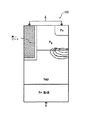
図11Aは基板240上で成長するエピタキシャル("epi")の層242を示している。トレンチ250はepi層242中に形成される。ゲート酸化物層244はトレンチ250の壁に沿っており、ゲート酸化物の層244の厚い部分246はトレンチ250の下部に位置している。トレンチ250はポリシリコン248で満たされる。ポリシリコン248上に酸化物層が存在しないことに注目して欲しい。図11Aの配列は中間的な構造かもしれず、プロセスの後の段階でポリシリコン248上に酸化物の層を形成することができた。ポリシリコン248は、典型的には高いドーピング濃度でドーピングされる。それは概ね平坦な上面をもって形成されてもよく、すなわち様々な手段によりシリコンepi表面と平坦になる。表面を平坦にする1つの方法は、ポリシリコン層をより大きな厚さに被着させ、次にそれをエッチバックすることである。表面を平坦にする別の方法は、トレンチを満たすために必要とされる量よりも厚くポリシリコンを被着させ、化学的な方法で表面を平坦に磨くことである。平面は、後の製造過程で形成され得るステップの高さを減少させるのに望ましい。
【0037】
図11Bはポリシリコン層248上に酸化物の層252を伴った構造を示す。酸化物層252の側縁がトレンチ250の壁に対応していないので、酸化物層252はマスク及びエッチング段階で大部分が形成されても良い。酸化物層252は、(例えば化学蒸着で)被着されるか、熱成長されるか、若しくはそれらのいくつかの組み合わせであっても良い。図11Cは、出願番号09/296,959(ここで言及したことで本出願の一部とする)に従って成長する酸化物層254を示す。酸化物の層254の側面は一般的にトレンチ250の壁と共に並び、酸化物層254はトレンチ250を下に向かって延在する。ポリシリコン層248はトレンチ250中にこのように埋め込まれる。図11B及び11Cの実施例は、ともにトレンチ底部に厚いゲート酸化物領域246を有する。
【0038】
図12は、本発明によるゲートトレンチの製造に使用することができる複数のプロセスの流れの概略図である。これらのプロセスの流れの詳細については、図13-20に示されている。図12は、フォトレジストマスク若しくは硬いマスクを用いてトレンチを形成し、続いて方向性酸化物被着を行い、それを選択的エッチング、ディップバック(dipback)または選択的酸化のいずれかで平坦化することがブロック図の形式で示している。選択的酸化は方向性被着なしに使用することができる。最後にトレンチは、1段階若しくは2段階プロセスを用いてポリシリコンで満たされる。
【0039】
更に詳しくは、図12の左側で開始されるトレンチ形成のための2つの選択肢が存在する。図13-18に示される1つの選択肢では、トレンチは後で取り除かれるマスクを使用して形成され、従ってこのマスクは他の処理過程に対しては基準として利用できない。別の選択肢は、上記した出願番号09/296959に説明されているように、トレンチを形成するのに“硬い”マスクを使用することであり、この硬いマスクはプロセスの後の方でも基準として用いられる。この選択肢については概ね図19と20で説明する。トレンチが形成された後、通常、犠牲酸化物層をトレンチの壁上に成長させ、その後取り除く。酸化物のライニングが次にトレンチの壁に形成されてもよい。この段階はシリコン上面の硬いマスクの有無にかかわらず、その壁に一様な酸化物層を有するトレンチを生ずる。
【0040】
次に、いわゆる方向性誘電体被着に進んでもよい。方向性誘電体被着によって、トレンチの底部にトレンチの側壁より多くの酸化物が被着される。次に3つの選択肢が存在する。図16に示されるように選択的エッチバックが実行可能であり、厚い酸化物がトレンチ下部に残り、トレンチの側壁からは酸化物を除去することが可能となる。図13-15に示されるように、一つの方法ではトレンチの側壁から酸化物の層を取り除くために“ディップバック(dipback)"を実行しうる。最終的に、図17A及び18で示されるように、1つの方法では、ポリシリコン層がトレンチの底部で形成され次にトレンチの底部で追加的酸化物を形成するために酸化されるような選択的酸化を実行することができる。ポリシリコン層の選択的酸化は、方向性誘電体被着に加えてまたはその代わりに実行することができる。
【0041】
プロセスのこの段階において、厚い酸化物の層が下部にあるトレンチが形成される。半導体の上面に“硬い”マスクがある場合もない場合もある。次に、薄い酸化物層がトレンチの壁面で成長し、トレンチがポリシリコンで満たされる。ポリシリコンは1層構造で被着されても良く、若しくは被着の間にエッチバックを伴って2層で被着されても良い。ポリシリコンを2段階のプロセスで被着することは、トレンチの間の“メサ”へドーパントを導入し、より低濃度にドープされたポリシリコン層がウエハの表面に得られるようにし、ダイオード、抵抗及び他のポリシリコンデバイスを形成する上で有益であり得る。
【0042】
最後に、ガラス層が被着され、コンタクト開口がガラス層に形成される。
【0043】
図13A-13Nは、酸化物の“ディップバック”法を用いるプロセスを表す。プロセスは基板260上に形成されたepi層262から始まる。マスク層264はepi層262の上面に形成され、トレンチが形成される開口を備える。マスク層264はフォトレジスト若しくは複数のその他の材料でも良く、それらは酸化物層266の上部に形成されてもよい。トレンチ268が、図13Aに示されるように従来のプロセスを用いて形成される。
【0044】
図13Bでは、犠牲酸化物層270がトレンチの表面に形成される。そして図13Cに示されるように犠牲酸化物層270は取り除かれる。犠牲酸化物層270は100オングストロームから1000オングストロームの厚さであって良く、典型的には300オングストロームのオーダの厚さであってよい。通常、酸化環境で10分から5時間、800度から1100度で加熱することで構造が形成され得る。周辺環境は酸素、若しくは酸素及び水素のいずれかであり得る。周囲が酸素と水素の組み合わせならば、反応は水蒸気を発生させ、これが酸化物の性状及び成長率に影響し得ることから、それは“ウエット”酸化であると考えられる。
【0045】
その後、任意に酸化ライニング272がトレンチ268上に形成される。ライニング272は、100オングストロームから600オングストロームの範囲の厚みを有し得る。ライニング272は、被着される酸化物が、荷電状態にある可能性があるシリコンに直接接触するのを防止する。この問題は、特にシリコンと被着酸化物との間の境界面に生じ得る。トレンチの壁上のきれいな酸化物の層の追加により、電荷状態が減少する。
【0046】
図13Eに示されるように、電界がepi層262の表面の上に適用され、誘電体イオンが形成され、それが電界によってトレンチ268へ下向きに向けられる。望ましくは、プラズマCVD(plasma-enhanced chemical vapor deposition)チャンバーがこのプロセスに用いられる。電界が誘電体イオンを下向きに加速するので、それらはトレンチ268の底部を含む水平面に優先的に被着する。酸化物の化学蒸着は、酸素とシラン、ジクロロシラン、若しくは四塩化珪素との気体状態での化学反応を含む。酸素のソースとしては通常nitreous酸化物があげられ、シランはシリコンのソースである。プラズマCVD機器は、Novellus Systems及びApplied Materialsのような会社のものが利用可能である。
【0047】
方向性を有する被着を達成する別の方法は、酸化物でコーティングされたターゲットよりウエハへ酸化フィルムをスパッタリングすることである。スパッタリングは運動量輸送プロセスであるので、被着は直線的に起こる。
【0048】
図13Fに示されるプロセスの結果、トレンチ268の内部及び外部に酸化物層270が形成される。酸化物層270は、トレンチ268の側壁よりも底部で厚いことに注目して頂きたい。それはepi層262の平坦な表面上でもまたより厚い。化学蒸着以外の例えばスパッタリングの様なプロセスもまた酸化物層270の生成に用いられ得る。
【0049】
層270は、例えばリン被着ガラス若しくは硼素リンシリコンガラスのような酸化物以外の材料からも形成することができる。また、それは低い誘電率Kを有する高分子やポリイミドの様な他の材料から成ることもできる。誘電率を低下させるべく、層270中に気泡を導入しても良い。
【0050】
図13Gでは、トレンチ268の側壁部分を取り除くため酸化物層270がエッチバックされ、ディップ(dip)バックされている。酸化物層270の底部分274がトレンチ268の底部に残る。図13Hに示されるように、トレンチ268の側壁に薄い酸化物層276を形成するべく、そのとき構造は加熱される。ポリシリコン層278は、次にトレンチ268を満たし、構造の上面からあふれるべく被着される。これは、図13Iに示される。
【0051】
図13Jに示されるように、ポリシリコン層278は次にepi層262の上面と概ね同一表面になるまでエッチバックされる。次に、トレンチの側壁で酸化物層276を過剰にエッチングしないように注意して、epi層262の表面の酸化物層270の一部が取り除かれる。このステップの結果は、図13Kに示される。酸化物層276上でわずかに突出したポリシリコン層278を有することで、酸化物層276の除去の回避が最適に実行される。図13Lでは, ポリシリコン層278の上面を含む構造の全体上面が酸化され、酸化物層280を形成する。
【0052】
図13Mに示されるように、ガラス層282が酸化物層280の表面を覆い、ガラス層282と酸化物層280は、その後epi層262にコンタクト開口を形成するべくパターン化されエッチングされ、図13Nで見せられる構造をもたらす。
【0053】
図14A-14Fは、図13Iで示された構造より開始される代替プロセスの流れを示すものである。図14Aは図13Iに対応している。図14Bに示されるようにポリシリコン層278はエッチングされて、次にポリシリコン層278の残存部分の上面は、図14Cに示されるように酸化物層290を形成するために酸化される。ガラス層292が、次に図14Dに示されるように構造の全体の表面にわたって被着される。マスク層294がガラス層292の上面に形成され、図14Fに示されるように、コンタクト開口を形成するべく層270および292がエッチングされる。次に、マスク層294が取り除かれる。
【0054】
図15A-15Fは、図13Iで示される構造で開始される別の代替手段を再び表す。図15Aは図13Iに対応している。図15Bに示されるように、ポリシリコン層278はトレンチの内部のレベルにエッチバックされる。次に、第二のポリシリコン層300が、図15Cに示されるように全体の構造に被着される。ポリシリコン層300は次にエッチバックされるが、トレンチの上部のコーナーに於いて酸化物層276の一部が露出しないように注意を必要とする。.結果として得られる構造は、図15Dに示される。次に酸化物層270が図15Eに示されるように取り除かれ、酸化物層302が構造の全体表面にわたって形成される。そして、ガラス層304が酸化物層302の上に被着され、図15Fで示される構造が得られる。
【0055】
図16A-16Eは図13Fの構造から始まる代替プロセスを表す。図16Aは図13Fに対応している。この構造を覆うようにフォトレジスト層が形成され、成長され、すすがれ(rinsed)、それによって構造の上面のフォトレジスト層は取り除かれ、トレンチ268の底部に残るようにされる。これは、トレンチ268の底部からはフォトレジストが除去されにくいという事実を利用したものである。トレンチ268の底部にフォトレジスト層310の残存部分を有する、結果として生じる構造が図16Bで示される。酸化物エッチングが、次にトレンチ268の側壁から酸化物層270の一部分を取り除くべく実行される。そののち徹底的なすすぎがフォトレジスト310を取り除くべく働き、図16Cで示される構造を提供することとなる。次に、構造はトレンチの側壁に薄い酸化物層312を形成するために酸化され、トレンチは図16D及び16Eに示されるようにポリシリコン層314で満たされる。図15A-15Cに示されるように、二段階のポリシリコン被着を実行されても良い。
【0056】
図17A-17Fは、図13Fで表される構造で開始される更に別の代替実施例のプロセスを示している。図17Aは図13Fに対応している。図17Bに示されるように、犠牲ポリシリコン層320は被着される。小さい部分322のみがトレンチ268の底部に残るまで、ポリシリコン層320はエッチバックされる。そして、ポリシリコン層320の一部322は酸化される。低温ポリシリコン酸化物はシリコンが単結晶と比較して急速に酸化しているので、低温(例えば、700〜950度)酸化プロセスが使用されている。したがって酸化物はトレンチ268の側壁より高速で部分322に形成される。結果として生じる構造は、トレンチ268の底部に酸化物層324を備える形で図17Bに示される。酸化物層270の一部は、図17Eに示されるようにトレンチ268の側壁から取り除かれ、薄いゲート酸化物層326が図17Fに示されるようにトレンチ268の側壁で形成される。
【0057】
図18A-18Fは、図13Bで示される構造で開始される別の代替のプロセスを表す。図18Aは図13Dに対応し、酸化物ライニング272が形成されている。図13Eに示されるような方向性誘電体の被着を利用する代わりに、犠牲ポリシリコン層330が図18Bに示されるように被着される。図18Cに示されるように、小さい部分332のみがトレンチ268の底部に残るまで, ポリシリコン層330がエッチバックされる。そして構造が上述されるように低温の酸化にかけられ、図18Dに示されるようにポリシリコン部分332を酸化物層334に変える。次に図18Eに示されるように、酸化物ライニング272が構造の側壁と上面から剥離され、ゲート酸化物336がトレンチ268の側壁で成長する。結果として生じる構造が図18Fで示される。
【0058】
図19A-19Iは上述の出願番号09/296,959で述べられたスーパー自己整列プロセスを含むプロセスを表している。構造は基板340上で成長するepi層342中で形成される。薄い酸化物層346がepi層342の表面に形成され、それは窒化シリコンなどの硬いマスキング材料の層344で覆われている。図19Aに示されるように、開口が窒化物層344と酸化物層346中でエッチングされている。
【0059】
図19Bに示されるように、従来のプロセスを使用してトレンチ348がepi層342中にエッチングされた。犠牲酸化物層(図示せず)トレンチ348の壁に形成され、取り除かれる。図19Cに示されるように、次に酸化物ライニング350がトレンチ348の壁面に形成される。図19Dに示されるように図13Eに関連して上述された種類の方向性被着が働き、酸化物層352が形成される。図19E及び19Fに示されるように、酸化物層352及び酸化物ライニング350の一部はトレンチ348の側壁から取り除かれる。この事は、例えば170HFの酸に構造を浸すことで行われる。次にゲート酸化物層356が形成され、トレンチがポリシリコン層358で満たされる。これらのステップは図19G及び19Hに示されている。
【0060】
そして、図.19Iに示されるように、ポリシリコン層358は薄い酸化物層346の表面の上のレベルまでエッチバックされる。図19Jでは、厚い酸化物層352が窒化物層344上より取り除かれ、ポリシリコン層358がトレンチ348のエッジで薄い酸化物層356を保護している。次に構造はアニールされ、ポリシリコン層358の一部が酸化され、図19Kに示されるようにトレンチの上側領域で厚い酸化物層360を形成する。最終的には、図19Lに示されるように窒化物層344は取り除かれる。
【0061】
図21A-20Fは、一方がアクティブアレイであり、他方がゲートバスの一部であるような2つのトレンチを伴う2段階のポリシリコンプロセスを示している。プロセスは、ポリシリコン層388がトレンチの374Aと374Bを満たしている状態で、図19Hに示されたポイントで開始する。トレンチの374Aと374Bの底部で、厚い酸化物層384が形成された。窒化けい素層374が、epi層372表面を覆い、窒化物層374は酸化物層382で覆われている。
【0062】
ポリシリコン層388は、図20Bに示されるようにエッチバックされ、酸化物層382は取り除かれる。第二のポリシリコン層390がポリシリコン層388上に被着され、窒化物若しくはポリイミドで形成された“硬い”層392が例えば2番目のポリシリコン層390の上に被着される。結果として生じる構造体は図20Cに示される。
【0063】
図20Dに示されるように、ポリシリコン層390及び硬い層392はアクティブアレイ(トレンチ374A)領域よりエッチングされ、ゲートバス(トレンチ374B)領域中にはそれらの層が残る。構造はトレンチ374Aに於けるポリシリコン層388を酸化するべく加熱され、トレンチの上部領域に厚い酸化物層394を生成する。同時に、酸化物層396が第二のポリシリコン層390の露出エッジで形成される。この構造は図20Eに示される。
【0064】
最終的には、硬い層374及び392の露出した部分が取り除かれ、図20Fで示される配置を得ることとなる。
【0065】
図21A-21E及び22A-22Cは、回避する必要のある二つの問題を示している。図21Aは、トレンチの壁に沿った犠牲酸化物層400、及びepi層の上面上の 薄い酸化物層404および窒化物層402を示す。図21Bに示されるように、犠牲酸化物層400の排除プロセスに於いて、薄い酸化物層404の一部が窒化物層402の下で取り除かれてしまう。この問題の解決法は、酸化物のオーバーエッチング時間を最小にすること、若しくは15〜90オングストロームほどの可能な限り薄い酸化物層404を用いることである。
【0066】
トレンチの底部に於ける厚い酸化物層408の構成を伴う、ゲート酸化物層406が形成される場合、ゲート酸化物層406は図21Cに示されるようにトレンチの上部のコーナーを十分には覆わないかもしれない。図21D及び21Eは、ポリシリコン層412が被着され、窒化物層414を用いて、素子のアクティブアレイからはエッチバックされた後の構成を示し、トレンチの上部のコーナーでポリシリコン層412とepi層とを隔離させる薄い酸化物層を示している。
【0067】
図22A-22Cは、別の潜在的な問題領域を示す。図22Aは図19Dで示されるのと同じ段階の素子を表し、方向性被着された厚い酸化物層352を備え、トレンチの底部に厚い部分354を形成する。図22Bに示されるように、トレンチの側壁から酸化物を取り除くプロセスに於いて、薄い酸化物層346の一部は窒化物層344の下部より除去される。次に、ゲート酸化物層356が成長し、トレンチの上部コーナーに於ける酸化物層の一部は極度に薄く、このことは、酸化物の欠陥及びゲートとepi層の間の短絡を導き得る。この問題は図22Cに示されている。ここでも、この解決策は、酸化物のオーバーエッチングを最小化すること、若しくは代わりに、化学的には等方性エッチングをなすプラズマエッチングを用いることである。
【0068】
図23Aは、図21Eに示されるようにポリシリコンが窒化物層の下に形成されたキャビティを満たす場合に生じる問題を示すものである。ポリシリコン層420の一部420Aはトレンチ外部に延在し、epi層に接触するように後に被着される金属層に短絡してしまう。酸化の間、酸化物422は窒化物オーバハングの下に充填されたシリコンを侵食しない。従って窒化物を除去すると、ゲートが露出し、ソース金属に短絡することとなる。図23Bはポリシリコン層の一部420Bが酸化物によって主たるポリシリコン層420より隔絶される変形例を表す。図23Cはポリシリコン層420が上に突出したスパイク420Cを形成する事例を示し、それによってゲートポリシリコン層420と後に被着される金属層との間で短絡が生じやすくなっている。やはり、窒化物の下を満たすポリシリコン層は、酸化の後も残されており、ゲート−ソース間の短絡の可能性がある。
【0069】
図23Dは、短絡の生じた素子のゲートI-V特性を示す。抵抗が小さい場合は「ハード」短絡.と呼ばれる。図23Eは「ソフト」またはダイオード的短絡の特性を示している。金属がポリシリコンゲートの上面に直接接触するハード短絡とは異なり、ダイオード的な短絡は図23Fに示されるゲートバス領域中で発生し得る。このタイプの動作不良では、ポリシリコンがシリコンメサに触れるようなところには全てN+領域またはプルームがPボディ中にドープされ、それによって図23Gに模式的に示すように寄生ダイオード及びMOSFETが形成されている。
【0070】
図24A-24Fは、オーバーエッチングされた第1ポリシリコン層や形状不良または歪んだトレンチによってダイオード短絡を生じさせるプロセス機構を示している。図24Aではアクティブセル及びゲートバス領域がN+ドープされたポリシリコンの第一の層で満たされ、次にエッチバックされ、図24Bで示される構造を生成する。ポリシリコンのエッチバックが一様なものでなければ、トレンチ酸化物の一端が図24Cに示されるように露出するかもしれず、それは次に上部酸化物を取り除くディップ(dip)過程の間に浸食され、エッチングされる。図24Dでは、第二のポリシリコン層が被着され、マスクキングでパターン化され、左にはアクティブセル右にはゲートバスが残る。上面の酸化の後、図24Eで示されるように左のアクティブセルは酸化され、自己修復がなされるが、ゲートバス領域においては、シリコンに接しているポリシリコンによってN+プルームがドープされ、図24Fのダイオード的ゲート短絡につながる。ポリシリコンの一様なエッチバック若しくは一様な形状のトレンチによって、本問題は避けられる。
【0071】
図25A-25Hは、窒化物側壁スペーサの使用によって問題を回避する為のプロセスを記述したものである。このプロセスは基板500上で成長するepi層502と共に開始される。薄い酸化物層504がepi層502の上面で成長し、窒化物層506(若しくはその他の別の“硬い”層)及び2番目の酸化物層508が、酸化物層504上に連続して形成される。したがって、層504、506、および508は、本分野に於いては既知の、酸化物−窒化物−酸化物(ONO)サンドイッチを形成する。結果として生じる構造が図25Aで示される。図25Bに示されるように、開口がONOサンドイッチ中にエッチングされる。次に窒化物層510が構造の上部を被着し、図25Cに見られるような配列をもたらす。窒化物層は不均等にエッチングされる。窒化物層510の垂直方向の厚さがONOサンドイッチのエッジよりも大きいので、異方性エッチングが酸化物層504及び窒化物層506の露出エッジに於いて側壁スペーサ512を残す。この構造は、酸化物層508の除去の後、図25Dに示される。
【0072】
次に図25Eに示されるように、次にトレンチ514がエッチングされ、典型的な犠牲酸化物層(図示せず)が形成され除去される。図25Fは、酸化物層516の方向性被着後の構造を示し、それはトレンチ514の底部に厚い酸化物層518を残す。この事は、ゲート酸化物層520の形成後に行われる。その後、トレンチはポリシリコン層522で満たされ、下の酸化物層520を攻撃しないよう注意してエッチバックされる。ポリシリコンとシリコンがほぼ接触する上部領域は、後のプロセスで更に酸化されることになる。また、或る程度の酸化物が、”鳥のくちばし“の様な窒化物の側壁キャップ下で成長する。この構造は図25Gに示される。酸化物層516は取り除かれ、図25Hで示される実施例が提供される。
【0073】
図26A及び26Bに示されるように、トレンチの側壁におけるゲート酸化物の成長は、図26Bのゆがみ530で示されるような、トレンチの側壁に於ける“ゆがみ”を導きうる。図26Aに示されるように、この問題は酸化物がトレンチの露出側壁532上で一様に成長することである。しかし、厚い酸化物534がトレンチの底部で始まる場所では、構造の外面的形態により、酸化が直線的に進行しない。この事は、ゆがみ530で厚さが減少した酸化物層を生成する。
【0074】
この問題に対する解決法が、図27A-27Dにおいて示される。図27Aは上述されるように、酸化物ライニング540の熱成長及び酸化物層542の方向性被着の後の構造を示す。ライニング540及び層542は、図27Bに示されるようにトレンチの側壁より除去される。構造体は170HFの酸に浸され(dip)る。被着された酸化物が熱成長した酸化物よりも早くエッチングされるので、浸漬の後にライニング540の上面が酸化物層542の上面よりわずかに上にある状態で、構造は図27Cのようになる。ゲート酸化物層がトレンチの側壁で熱成長する場合、結果的に生じる酸化物は一様な厚さを有する。トレンチの壁には“ゆがみ”は存在しない。図27Dは、ゲート酸化物層544がトレンチの側壁で成長した後の配置を表す。点線は、酸化に先立ったシリコンのもとの位置を示す。
【0075】
図28-33は、本発明の原理利用して製造可能な、様々な素子を示している。
【0076】
図28は、底が平らなP-ボディ領域、及びepi層及び基板間の境界面にN埋込層を有するパワーMOSFETを表す。図28は、トレンチ間のメサ全体に渡って延在するコンタクトと厚いトレンチ底部の酸化物とを組み合わせた素子を示している。なお、コンタクトマスクや平坦でない上面酸化物層を用いることも可能である。図29は、それぞれのMOSFETセルが、Buluceaらの米国特許番号5,072,266に示されたような深いP+領域を含むことを除いて、図28に示されるものと同様のMOSFETを示している。図30の実施例は、MOSFETセルの中に底が平らなP+領域を有し、更に、MOSFETセルの電圧クランプをするのに用いられる深いP+領域を含むダイオードセルを有する。このような構造は、出願番号08/846,688において記述されており、この出願はここに言及したことで本出願の一部とする。
【0077】
図31に示される素子では、Pボディ領域と各MOSFETセルに於ける金属層との間のコンタクトが存在しない。その代わり、米国特許番号5,877,538でWilliamsらによって述べられているように、第三の方向でボディと接触する。この出願も、ここで言及したことで本願の一部とする。MOSFETセルの1つが、トレンチの底部に於ける電界の強度を制限するために、深いP+領域を有する事に注目して頂きたい。さらに、自己整列コンタクトを用いる平坦な上部酸化物層が好ましいが、必須というわけではない。
【0078】
図32の実施例では、トレンチはN埋込層まで延在し、厚い酸化物領域のみが厚くドープされた埋込層と重なる。
【0079】
図33の実施例は、Williamsらによって米国特許番号5,856,692で発表された一つのような蓄積モードMOSFET(ACCUFET)であり、ここで言及したことで本願の一部とする。
【0080】
図34は、従来のコンタクトマスクおよび組み込まれた厚いトレンチ底部の酸化物を用いたトレンチMOSFETのための、プロセスの流れを示した概念図である。プロセスの過程は、通常ドレイン及び深いボディ領域の構築、トレンチのエッチング及びゲートの構築、ボディ及びソース領域の埋込、コンタクトの開口及び金属層の被着を含む。図34では、方形の角が欠けたものは、オプションの過程を表す。したがって、注入若しくは注入及び拡散によるより深いボディ領域の導入は、このプロセスと一致している。
【0081】
このプロセスが、図35A-35Lに示されている。トレンチ552は、Nepi層550中にマスクとして酸化物層554を用いて形成される。酸化物ライニング556がトレンチ552の壁に形成され(図35B)、上述したように方向性の酸化物被着がなされ、トレンチの底部で厚い部分560を有する酸化物層558を形成する(図35C)。トレンチ552の側壁は次にエッチングされ(図35D)、ゲート酸化物層がトレンチの壁552上で熱成長する(図35E)。
【0082】
そして、ポリシリコン層564が、トレンチ552(図35F)を満たすべく被着される。ポリシリコン層564は、トレンチ内部へとエッチバックされる(図35G)。酸化物層566が構造の上面に被着され、ポリシリコン層564の上面へトレンチに向かって広がる(図35H)。次に酸化物層566がエッチバックされ、ほう酸の様なP型ドーパントが、Pボディー領域568を形成するべく注入される。その時、上面はマスクされ(図示せず)、ヒ素若しくはリンのようなN形ドーパントが、N+ソース領域570を形成するために注入される。別の酸化物層572が上面に被着されパターン化され、図35Lに示された構造を得る。コンタクトは上部金属で埋めることができるが、代わりにタングステンのような平坦化金属若しくはTi/TiNの様なバリア金属で満たすこともできる。
【0083】
図36-39は、ポリシリコンゲートの断面が”鍵穴“の形状を成すような複数の実施例を示す。より厚いゲート酸化物が、トレンチの底部に沿って延在するだけでなく、Pボディー領域及びN epi層の間の接合に向かいトレンチの側壁に沿ってもまた延在している。トレンチの側壁に沿った厚くされたゲート酸化物は、接合に於ける電界を緩和するのを助ける。
【0084】
図36は、平底のPボディ領域およびMOSFETセル間で周期的間隔で組み込まれたダイオードセルを有するMOSFETを示す。MOSFET好ましい変形例では、鍵穴型のゲートが採用される。図37は、Pボディーが表面に延在しないが、代わりに第三の方向で接触する様な実施例を示す。浅いP+領域を、メサ中のN+ソース領域よりも深い所で見ることができる。図38はトレンチが、epi層及び基板との間の境界面に形成されたN埋込層中に向かって延在している実施例を示す。図39はPボディが第三の方向で接続され、トレンチがN埋込層中に延在する実施例を示す。
【0085】
鍵穴の形状のトレンチを有する素子の形成のプロセスの流れが図40A-40Lに示される。プロセスは基板600上で成長したepi層602で開始される。図40Aに示されるように、酸化物層604がepi層602の上面に形成される。酸化物層604はパターン化され、図40Bに示されるようにエッチングされる。犠牲な酸化物層(図示せず)が次にトレンチ606の壁で成長する(図40Cで、示される)。
【0086】
図40Dと40Eに示されるように、ポリシリコン層610がトレンチ606を満たすために被着され、次にトレンチの底に一部612が残るようにエッチバックされる。酸化物のライニング608は、図40Fに示されるようにその時トレンチ606の側壁からエッチングされる。図40Gに示されるように酸化物ライニング608の上面より低い位置にポリシリコン層612の上面を押し下げるべく、その時異方性シリコンエッチングが実行される。次に熱酸化プロセスが用いられ、トレンチ606の壁面上の酸化物層616を形成し、ポリシリコン層612の上面には酸化物層618を形成する。図40Hに結果として生じる構造物が示される。酸化物層618がその時エッチングされ、酸化物層616の一部がそのプロセス中で除去され、図40Iに示される構造が生成される。
【0087】
次に、図40Jに示されるように第二のポリシリコン層619が構造の全体に被着される。図40Kに示されるように、ポリシリコン層619はエッチバックされる。図40Lに示されるように、ポリシリコン層619の上面は、次に酸化される。
【0088】
このプロセスの変形例が、図41A-41Fに示される。酸化物ライニング608がトレンチの壁面で形成された後、図40Cに示されるように、フォトレジスト層が適用され、成長し、取り除かれ、そしてトレンチ606の底部に一部分630のみが残る。この様子が、図41Aに示されている。図41Bに示されるように酸化物ライニング608は、トレンチ606の壁面よりエッチングされ、フォトレジスト層630の一部がトレンチの底部より取り除かれる。この事で、図41Cに見られる構造が得られる。
【0089】
図41D及び41Fに示されるように、酸化物層632がトレンチ606の壁面で熱成長し、トレンチ606はポリシリコン層634で満たされる。ポリシリコン層634は、epi層602の上面のレベルまでエッチバックされる。次にポリシリコン層634は熱酸化され、図41Fで示される素子が提供される。
【0090】
図42A-42Cは、従来技術のトレンチの側壁に沿った電界強度と、本発明によるそれとの比較を示す。図41Aは、先行技術の素子で、電界が、ボディ−ドレイン接合及びゲート電極底部で各々発生する二つの鋭いピークを有することを示す。図42Bは、トレンチの底部に厚い酸化物層を有する素子を示す。示されるように、電界はなおもボディ−ドレイン接合部に鋭いピークを有するが、先行技術のそれと比較してゲート電極の底部に於けるピークは幾分低い。最終的に、図42Cは、鍵穴形状のゲート電極を有する素子を示す。この場合でも、電界はボディ−ドレイン接合部でピークに到達するが、ゲート電極の底部に於ける鋭いピークは取り除かれている。
【0091】
本発明に基づいて複数の実施例が記述されているが、それらはあらゆる点で単なる例示に過ぎず、限定的に解釈してはならない。
【図面の簡単な説明】
【図1】 図1は電圧クランプとして機能する深いP+ダイオードを有する従来技術のトレンチパワーMOSFETの断面図である。
【図2】 図2は平坦なボディ−ドレイン接合を有する従来技術のトレンチパワーMOSFETの断面図である。
【図3】 図3は平坦なボディ−ドレイン接合を含む複数のMOSFETセル中に分布された電圧クランプを有する従来技術のトレンチパワーMOSFETの断面図である。
【図4A】 図4Aは厚いゲート酸化物層を有するMOSFETにおける電界輪郭を示す断面図である。
【図4B】 図4Bは薄いゲート酸化物層を有するMOSFETにおける電界輪郭を示す断面図である。
【図4C】 図4Cはなだれ降伏(アバランシェブレークダウン)開始時の、厚いゲート酸化物層を有するMOSFETにおけるイオン化輪郭を示す断面図である。
【図4D】 図4Dはなだれ降伏(アバランシェブレークダウン)開始時の、薄いゲート酸化物層を有するMOSFETにおけるイオン化輪郭を示す断面図である。
【図4E】 図4Eは、電圧クランプとして使用される深いP+領域を含む素子におけるイオン化輪郭を示す断面図である。
【図4F】 図4Fは、異なるドーピング濃度を有するエピタキシャル層に形成されたMOSFETにおける降伏電圧をゲート酸化物の厚みの関数として示したグラフである。
【図4G】 図4Gは逆平行ダイオードクランプを備えたトレンチパワーMOSFETの模式図である。
【図5A】 図5Aは正方形のトレンチコーナーを有するトレンチパワーMOSFETにおけるイオン化輪郭を示す断面図である。
【図5B】 図5Bは丸められたトレンチコーナーを有するトレンチパワーMOSFETにおけるイオン化輪郭を示す断面図である。
【図6A】 図6Aは平坦なボディ−ドレイン接合を有するトレンチパワーMOSFETにおける電界輪郭を示す断面図である。
【図6B】 図6Bは平坦なボディ−ドレイン接合を有するトレンチパワーMOSFETにおける等電位線を示す断面図である。
【図6C】 図6Cは平坦なボディ−ドレイン接合を有するトレンチパワーMOSFETにおける電界線を示す断面図である。
【図6D】 図6Dは平坦なボディ−ドレイン接合を有するトレンチパワーMOSFETにおける電流の流れ線を示す断面図である。
【図6E】 図6Eはターンオン時のトレンチパワーMOSFETにおけるイオン化輪郭を示す断面図である。
【図6F】 図6Fは、異なるゲート電圧にあるパワーMOSFETに対するI−V曲線を示したグラフであり、衝突イオン化によって維持電圧がどのように低下するかを示している。
【図7A】 図7AはパワーMOSFETのためのゲート充電回路の模式図である。
【図7B】 図7BはパワーMOSFETにゲート駆動電流をステップ関数的に加えること示すグラフである。
【図7C】 図7Cは、図7Bの条件の下でゲート電圧及びドレイン電圧がどのように変化するかを示すグラフである。
【図7D】 図7Dは、図7Bの条件の下でドレイン電流がどのように変化するかを示すグラフである。
【図7E】 図7Eはゲート電圧が電荷の関数としてどのように変化するかを示すグラフである。
【図7F】 図7FはパワーMOSFETがターンオンすると実効入力容量(effective input capacitance)がどのように変化するかを示すグラフである。
【図7G】 図7GはトレンチパワーMOSFETにおけるゲート容量の構成要素を示す断面図である。
【図7H】 図7Hは電極間容量を示すトレンチMOSFETの等価回路図である。
【図8A】 図8A〜図8Cは丸められたコーナーを有するゲートトレンチがどのように形成されるかを示す断面図である。
【図8B】 図8A〜図8Cは丸められたコーナーを有するゲートトレンチがどのように形成されるかを示す断面図である。
【図8C】 図8A〜図8Cは丸められたコーナーを有するゲートトレンチがどのように形成されるかを示す断面図である。
【図9A】 図9A〜図9Dはゲートトレンチのエッチング及びポリシリコンによるトレンチの充填のプロセスを示す断面図である。
【図9B】 図9A〜図9Dはゲートトレンチのエッチング及びポリシリコンによるトレンチの充填のプロセスを示す断面図である。
【図9C】 図9A〜図9Dはゲートトレンチのエッチング及びポリシリコンによるトレンチの充填のプロセスを示す断面図である。
【図9D】 図9A〜図9Dはゲートトレンチのエッチング及びポリシリコンによるトレンチの充填のプロセスを示す断面図である。
【図10A】 図10A〜図10Fは従来のトレンチパワーMOSFETの製造プロセスの断面図である。
【図10B】 図10A〜図10Fは従来のトレンチパワーMOSFETの製造プロセスの断面図である。
【図10C】 図10A〜図10Fは従来のトレンチパワーMOSFETの製造プロセスの断面図である。
【図10D】 図10A〜図10Fは従来のトレンチパワーMOSFETの製造プロセスの断面図である。
【図10E】 図10A〜図10Fは従来のトレンチパワーMOSFETの製造プロセスの断面図である。
【図10F】 図10A〜図10Fは従来のトレンチパワーMOSFETの製造プロセスの断面図である。
【図11A】 図11Aはトレンチの底部に厚い酸化物層を有するトレンチパワーMOSFETの断面図である。
【図11B】 図11Bは、半導体の上面にパターン化された厚い酸化物層を有する図11AのMOSFETを示す断面図である。
【図11C】 図11Cはトレンチの壁に整合された厚い上部酸化物層を備えた図11AのMOSFETを示す断面図である。
【図12】 図12は本発明に基づく多くのプロセスシーケンスを示す模式的なフロー図である。
【図13A】 図13A〜図13Nは、酸化物層の方向性被着を使用し且つ半導体材料の上面と同じレベルまでポリシリコンをエッチングする、トレンチ底部に厚い酸化物層を有するトレンチパワーMOSFETを形成するためのプロセスシーケンスを示している。
【図13B】 図13A〜図13Nは、酸化物層の方向性被着を使用し且つ半導体材料の上面と同じレベルまでポリシリコンをエッチングする、トレンチ底部に厚い酸化物層を有するトレンチパワーMOSFETを形成するためのプロセスシーケンスを示している。
【図13C】 図13A〜図13Nは、酸化物層の方向性被着を使用し且つ半導体材料の上面と同じレベルまでポリシリコンをエッチングする、トレンチ底部に厚い酸化物層を有するトレンチパワーMOSFETを形成するためのプロセスシーケンスを示している。
【図13D】 図13A〜図13Nは、酸化物層の方向性被着を使用し且つ半導体材料の上面と同じレベルまでポリシリコンをエッチングする、トレンチ底部に厚い酸化物層を有するトレンチパワーMOSFETを形成するためのプロセスシーケンスを示している。
【図13E】 図13A〜図13Nは、酸化物層の方向性被着を使用し且つ半導体材料の上面と同じレベルまでポリシリコンをエッチングする、トレンチ底部に厚い酸化物層を有するトレンチパワーMOSFETを形成するためのプロセスシーケンスを示している。
【図13F】 図13A〜図13Nは、酸化物層の方向性被着を使用し且つ半導体材料の上面と同じレベルまでポリシリコンをエッチングする、トレンチ底部に厚い酸化物層を有するトレンチパワーMOSFETを形成するためのプロセスシーケンスを示している。
【図13G】 図13A〜図13Nは、酸化物層の方向性被着を使用し且つ半導体材料の上面と同じレベルまでポリシリコンをエッチングする、トレンチ底部に厚い酸化物層を有するトレンチパワーMOSFETを形成するためのプロセスシーケンスを示している。
【図13H】 図13A〜図13Nは、酸化物層の方向性被着を使用し且つ半導体材料の上面と同じレベルまでポリシリコンをエッチングする、トレンチ底部に厚い酸化物層を有するトレンチパワーMOSFETを形成するためのプロセスシーケンスを示している。
【図13I】 図13A〜図13Nは、酸化物層の方向性被着を使用し且つ半導体材料の上面と同じレベルまでポリシリコンをエッチングする、トレンチ底部に厚い酸化物層を有するトレンチパワーMOSFETを形成するためのプロセスシーケンスを示している。
【図13J】 図13A〜図13Nは、酸化物層の方向性被着を使用し且つ半導体材料の上面と同じレベルまでポリシリコンをエッチングする、トレンチ底部に厚い酸化物層を有するトレンチパワーMOSFETを形成するためのプロセスシーケンスを示している。
【図13K】 図13A〜図13Nは、酸化物層の方向性被着を使用し且つ半導体材料の上面と同じレベルまでポリシリコンをエッチングする、トレンチ底部に厚い酸化物層を有するトレンチパワーMOSFETを形成するためのプロセスシーケンスを示している。
【図13L】 図13A〜図13Nは、酸化物層の方向性被着を使用し且つ半導体材料の上面と同じレベルまでポリシリコンをエッチングする、トレンチ底部に厚い酸化物層を有するトレンチパワーMOSFETを形成するためのプロセスシーケンスを示している。
【図13M】 図13A〜図13Nは、酸化物層の方向性被着を使用し且つ半導体材料の上面と同じレベルまでポリシリコンをエッチングする、トレンチ底部に厚い酸化物層を有するトレンチパワーMOSFETを形成するためのプロセスシーケンスを示している。
【図13N】 図13A〜図13Nは、酸化物層の方向性被着を使用し且つ半導体材料の上面と同じレベルまでポリシリコンをエッチングする、トレンチ底部に厚い酸化物層を有するトレンチパワーMOSFETを形成するためのプロセスシーケンスを示している。
【図14A】 図14A〜図14Fは、ポリシリコンが半導体材料の表面より低いレベルまでエッチングされた後酸化される、代替的なプロセスシーケンスを示している。
【図14B】 図14A〜図14Fは、ポリシリコンが半導体材料の表面より低いレベルまでエッチングされた後酸化される、代替的なプロセスシーケンスを示している。
【図14C】 図14A〜図14Fは、ポリシリコンが半導体材料の表面より低いレベルまでエッチングされた後酸化される、代替的なプロセスシーケンスを示している。
【図14D】 図14A〜図14Fは、ポリシリコンが半導体材料の表面より低いレベルまでエッチングされた後酸化される、代替的なプロセスシーケンスを示している。
【図14E】 図14A〜図14Fは、ポリシリコンが半導体材料の表面より低いレベルまでエッチングされた後酸化される、代替的なプロセスシーケンスを示している。
【図14F】 図14A〜図14Fは、ポリシリコンが半導体材料の表面より低いレベルまでエッチングされた後酸化される、代替的なプロセスシーケンスを示している。
【図15A】 図15A〜図15Fは、ポリシリコンが2段階に被着される、代替的なプロセスシーケンスを示している。
【図15B】 図15A〜図15Fは、ポリシリコンが2段階に被着される、代替的なプロセスシーケンスを示している。
【図15C】 図15A〜図15Fは、ポリシリコンが2段階に被着される、代替的なプロセスシーケンスを示している。
【図15D】 図15A〜図15Fは、ポリシリコンが2段階に被着される、代替的なプロセスシーケンスを示している。
【図15E】 図15A〜図15Fは、ポリシリコンが2段階に被着される、代替的なプロセスシーケンスを示している。
【図15F】 図15A〜図15Fは、ポリシリコンが2段階に被着される、代替的なプロセスシーケンスを示している。
【図16A】 図16A〜図16Eは、少量のフォトレジストがトレンチ底部の厚い酸化物をマスクするのに使用される、代替的なプロセスを示している。
【図16B】 図16A〜図16Eは、少量のフォトレジストがトレンチ底部の厚い酸化物をマスクするのに使用される、代替的なプロセスを示している。
【図16C】 図16A〜図16Eは、少量のフォトレジストがトレンチ底部の厚い酸化物をマスクするのに使用される、代替的なプロセスを示している。
【図16D】 図16A〜図16Eは、少量のフォトレジストがトレンチ底部の厚い酸化物をマスクするのに使用される、代替的なプロセスを示している。
【図16E】 図16A〜図16Eは、少量のフォトレジストがトレンチ底部の厚い酸化物をマスクするのに使用される、代替的なプロセスを示している。
【図17A】 図17A〜図17Fは、ポリシリコンがトレンチ底部近くのレベルまでエッチングされ、続いて酸化されるプロセスを示している。
【図17B】 図17A〜図17Fは、ポリシリコンがトレンチ底部近くのレベルまでエッチングされ、続いて酸化されるプロセスを示している。
【図17C】 図17A〜図17Fは、ポリシリコンがトレンチ底部近くのレベルまでエッチングされ、続いて酸化されるプロセスを示している。
【図17D】 図17A〜図17Fは、ポリシリコンがトレンチ底部近くのレベルまでエッチングされ、続いて酸化されるプロセスを示している。
【図17E】 図17A〜図17Fは、ポリシリコンがトレンチ底部近くのレベルまでエッチングされ、続いて酸化されるプロセスを示している。
【図17F】 図17A〜図17Fは、ポリシリコンがトレンチ底部近くのレベルまでエッチングされ、続いて酸化されるプロセスを示している。
【図18A】 図18A〜図18Fは、ポリシリコンが酸化される、代替的なプロセスを示している。
【図18B】 図18A〜図18Fは、ポリシリコンが酸化される、代替的なプロセスを示している。
【図18C】 図18A〜図18Fは、ポリシリコンが酸化される、代替的なプロセスを示している。
【図18D】 図18A〜図18Fは、ポリシリコンが酸化される、代替的なプロセスを示している。
【図18E】 図18A〜図18Fは、ポリシリコンが酸化される、代替的なプロセスを示している。
【図18F】 図18A〜図18Fは、ポリシリコンが酸化される、代替的なプロセスを示している。
【図19A】 図19A〜図19Lは、トレンチの壁と自己整合するゲート電極上に設けられた酸化物層を有するトレンチパワーMOSFETを製造するためのプロセスを示している。
【図19B】 図19A〜図19Lは、トレンチの壁と自己整合するゲート電極上に設けられた酸化物層を有するトレンチパワーMOSFETを製造するためのプロセスを示している。
【図19C】 図19A〜図19Lは、トレンチの壁と自己整合するゲート電極上に設けられた酸化物層を有するトレンチパワーMOSFETを製造するためのプロセスを示している。
【図19D】 図19A〜図19Lは、トレンチの壁と自己整合するゲート電極上に設けられた酸化物層を有するトレンチパワーMOSFETを製造するためのプロセスを示している。
【図19E】 図19A〜図19Lは、トレンチの壁と自己整合するゲート電極上に設けられた酸化物層を有するトレンチパワーMOSFETを製造するためのプロセスを示している。
【図19F】 図19A〜図19Lは、トレンチの壁と自己整合するゲート電極上に設けられた酸化物層を有するトレンチパワーMOSFETを製造するためのプロセスを示している。
【図19G】 図19A〜図19Lは、トレンチの壁と自己整合するゲート電極上に設けられた酸化物層を有するトレンチパワーMOSFETを製造するためのプロセスを示している。
【図19H】 図19A〜図19Lは、トレンチの壁と自己整合するゲート電極上に設けられた酸化物層を有するトレンチパワーMOSFETを製造するためのプロセスを示している。
【図19I】 図19A〜図19Lは、トレンチの壁と自己整合するゲート電極上に設けられた酸化物層を有するトレンチパワーMOSFETを製造するためのプロセスを示している。
【図19J】 図19A〜図19Lは、トレンチの壁と自己整合するゲート電極上に設けられた酸化物層を有するトレンチパワーMOSFETを製造するためのプロセスを示している。
【図19K】 図19A〜図19Lは、トレンチの壁と自己整合するゲート電極上に設けられた酸化物層を有するトレンチパワーMOSFETを製造するためのプロセスを示している。
【図19L】 図19A〜図19Lは、トレンチの壁と自己整合するゲート電極上に設けられた酸化物層を有するトレンチパワーMOSFETを製造するためのプロセスを示している。
【図20A】 図20A〜図20Fは、パワーMOSFETのアクティブアレイ内のトレンチゲート及びゲートバスを形成するためのプロセスシーケンスを示している。
【図20B】 図20A〜図20Fは、パワーMOSFETのアクティブアレイ内のトレンチゲート及びゲートバスを形成するためのプロセスシーケンスを示している。
【図20C】 図20A〜図20Fは、パワーMOSFETのアクティブアレイ内のトレンチゲート及びゲートバスを形成するためのプロセスシーケンスを示している。
【図20D】 図20A〜図20Fは、パワーMOSFETのアクティブアレイ内のトレンチゲート及びゲートバスを形成するためのプロセスシーケンスを示している。
【図20E】 図20A〜図20Fは、パワーMOSFETのアクティブアレイ内のトレンチゲート及びゲートバスを形成するためのプロセスシーケンスを示している。
【図20F】 図20A〜図20Fは、パワーMOSFETのアクティブアレイ内のトレンチゲート及びゲートバスを形成するためのプロセスシーケンスを示している。
【図21A】 図21A〜図21Eは、窒化物の下の薄い酸化物層をアンダーカッティングすることから生じ得る問題を示している。
【図21B】 図21A〜図21Eは、窒化物の下の薄い酸化物層をアンダーカッティングすることから生じ得る問題を示している。
【図21C】 図21A〜図21Eは、窒化物の下の薄い酸化物層をアンダーカッティングすることから生じ得る問題を示している。
【図21D】 図21A〜図21Eは、窒化物の下の薄い酸化物層をアンダーカッティングすることから生じ得る問題を示している。
【図21E】 図21A〜図21Eは、窒化物の下の薄い酸化物層をアンダーカッティングすることから生じ得る問題を示している。
【図22A】 図22A〜図22Cはこの問題の更なる例を示している。
【図22B】 図22A〜図22Cはこの問題の更なる例を示している。
【図22C】 図22A〜図22Cはこの問題の更なる例を示している。
【図23A】 図23A〜図23Gは、本発明に基づくパワーMOSFETの製造において生じ得る他の問題を示している。
【図23B】 図23A〜図23Gは、本発明に基づくパワーMOSFETの製造において生じ得る他の問題を示している。
【図23C】 図23A〜図23Gは、本発明に基づくパワーMOSFETの製造において生じ得る他の問題を示している。
【図23D】 図23A〜図23Gは、本発明に基づくパワーMOSFETの製造において生じ得る他の問題を示している。
【図23E】 図23A〜図23Gは、本発明に基づくパワーMOSFETの製造において生じ得る他の問題を示している。
【図23F】 図23A〜図23Gは、本発明に基づくパワーMOSFETの製造において生じ得る他の問題を示している。
【図23G】 図23A〜図23Gは、本発明に基づくパワーMOSFETの製造において生じ得る他の問題を示している。
【図24A】 図24A〜図24Fは、自己整合型素子において上面酸化物を除去する際に硬いマスクをアンダーエッチングすることから生じ得る問題を示している。
【図24B】 図24A〜図24Fは、自己整合型素子において上面酸化物を除去する際に硬いマスクをアンダーエッチングすることから生じ得る問題を示している。
【図24C】 図24A〜図24Fは、自己整合型素子において上面酸化物を除去する際に硬いマスクをアンダーエッチングすることから生じ得る問題を示している。
【図24D】 図24A〜図24Fは、自己整合型素子において上面酸化物を除去する際に硬いマスクをアンダーエッチングすることから生じ得る問題を示している。
【図24E】 図24A〜図24Fは、自己整合型素子において上面酸化物を除去する際に硬いマスクをアンダーエッチングすることから生じ得る問題を示している。
【図24F】 図24A〜図24Fは、自己整合型素子において上面酸化物を除去する際に硬いマスクをアンダーエッチングすることから生じ得る問題を示している。
【図25A】 図25A〜図25Hは、厚い底部酸化物層と窒化物サイドスペーサとを有するトレンチパワーMOSFETの製造プロセスを示している。
【図25B】 図25A〜図25Hは、厚い底部酸化物層と窒化物サイドスペーサとを有するトレンチパワーMOSFETの製造プロセスを示している。
【図25C】 図25A〜図25Hは、厚い底部酸化物層と窒化物サイドスペーサとを有するトレンチパワーMOSFETの製造プロセスを示している。
【図25D】 図25A〜図25Hは、厚い底部酸化物層と窒化物サイドスペーサとを有するトレンチパワーMOSFETの製造プロセスを示している。
【図25E】 図25A〜図25Hは、厚い底部酸化物層と窒化物サイドスペーサとを有するトレンチパワーMOSFETの製造プロセスを示している。
【図25F】 図25A〜図25Hは、厚い底部酸化物層と窒化物サイドスペーサとを有するトレンチパワーMOSFETの製造プロセスを示している。
【図25G】 図25A〜図25Hは、厚い底部酸化物層と窒化物サイドスペーサとを有するトレンチパワーMOSFETの製造プロセスを示している。
【図25H】 図25A〜図25Hは、厚い底部酸化物層と窒化物サイドスペーサとを有するトレンチパワーMOSFETの製造プロセスを示している。
【図26A】 図26A及び図26Bは、厚い底部酸化物にゲート酸化物層を形成する際に生じ得る問題を示している。
【図26B】 図26A及び図26Bは、厚い底部酸化物にゲート酸化物層を形成する際に生じ得る問題を示している。
【図27A】 図27A〜図27Dは、図26A及び図26Bに示した問題を避ける方法を示している。
【図27B】 図27A〜図27Dは、図26A及び図26Bに示した問題を避ける方法を示している。
【図27C】 図27A〜図27Dは、図26A及び図26Bに示した問題を避ける方法を示している。
【図27D】 図27A〜図27Dは、図26A及び図26Bに示した問題を避ける方法を示している。
【図28】 図28〜図33は、本発明に従って製造することができる様々なタイのプトレンチパワーMOSFETを示している。
【図29】 図28〜図33は、本発明に従って製造することができる様々なタイのプトレンチパワーMOSFETを示している。
【図30】 図28〜図33は、本発明に従って製造することができる様々なタイのプトレンチパワーMOSFETを示している。
【図31】 図28〜図33は、本発明に従って製造することができる様々なタイのプトレンチパワーMOSFETを示している。
【図32】 図28〜図33は、本発明に従って製造することができる様々なタイのプトレンチパワーMOSFETを示している。
【図33】 図28〜図33は、本発明に従って製造することができる様々なタイのプトレンチパワーMOSFETを示している。
【図34】 図34は、従来のコンタクトマスクを使用しつつ厚い底部酸化物層を備えたトレンチパワーMOSFETを製造するプロセスシーケンスのフロー図を示している。
【図35A】 図35A〜35Lは、図34のプロセスを示す断面図である。
【図35B】 図35A〜35Lは、図34のプロセスを示す断面図である。
【図35C】 図35A〜35Lは、図34のプロセスを示す断面図である。
【図35D】 図35A〜35Lは、図34のプロセスを示す断面図である。
【図35E】 図35A〜35Lは、図34のプロセスを示す断面図である。
【図35F】 図35A〜35Lは、図34のプロセスを示す断面図である。
【図35G】 図35A〜35Lは、図34のプロセスを示す断面図である。
【図35H】 図35A〜35Lは、図34のプロセスを示す断面図である。
【図35I】 図35A〜35Lは、図34のプロセスを示す断面図である。
【図35J】 図35A〜35Lは、図34のプロセスを示す断面図である。
【図35K】 図35A〜35Lは、図34のプロセスを示す断面図である。
【図35L】 図35A〜35Lは、図34のプロセスを示す断面図である。
【図36】 図36〜図39は、「鍵穴」状ゲート電極を有するトレンチパワーMOSFETを示す断面図である。
【図37】 図36〜図39は、「鍵穴」状ゲート電極を有するトレンチパワーMOSFETを示す断面図である。
【図38】 図36〜図39は、「鍵穴」状ゲート電極を有するトレンチパワーMOSFETを示す断面図である。
【図39】 図36〜図39は、「鍵穴」状ゲート電極を有するトレンチパワーMOSFETを示す断面図である。
【図40A】 図40A〜図40Lは、鍵穴状ゲート電極を有するMOSFETを製造するためのプロセスシーケンスを示している。
【図40B】 図40A〜図40Lは、鍵穴状ゲート電極を有するMOSFETを製造するためのプロセスシーケンスを示している。
【図40C】 図40A〜図40Lは、鍵穴状ゲート電極を有するMOSFETを製造するためのプロセスシーケンスを示している。
【図40D】 図40A〜図40Lは、鍵穴状ゲート電極を有するMOSFETを製造するためのプロセスシーケンスを示している。
【図40E】 図40A〜図40Lは、鍵穴状ゲート電極を有するMOSFETを製造するためのプロセスシーケンスを示している。
【図40F】 図40A〜図40Lは、鍵穴状ゲート電極を有するMOSFETを製造するためのプロセスシーケンスを示している。
【図40G】 図40A〜図40Lは、鍵穴状ゲート電極を有するMOSFETを製造するためのプロセスシーケンスを示している。
【図40H】 図40A〜図40Lは、鍵穴状ゲート電極を有するMOSFETを製造するためのプロセスシーケンスを示している。
【図40I】 図40A〜図40Lは、鍵穴状ゲート電極を有するMOSFETを製造するためのプロセスシーケンスを示している。
【図40J】 図40A〜図40Lは、鍵穴状ゲート電極を有するMOSFETを製造するためのプロセスシーケンスを示している。
【図40K】 図40A〜図40Lは、鍵穴状ゲート電極を有するMOSFETを製造するためのプロセスシーケンスを示している。
【図40L】 図40A〜図40Lは、鍵穴状ゲート電極を有するMOSFETを製造するためのプロセスシーケンスを示している。
【図41A】 図41A〜図41Fは、鍵穴状ゲート電極を有するMOSFETを製造するための代替的なプロセスシーケンスを示している。
【図41B】 図41A〜図41Fは、鍵穴状ゲート電極を有するMOSFETを製造するための代替的なプロセスシーケンスを示している。
【図41C】 図41A〜図41Fは、鍵穴状ゲート電極を有するMOSFETを製造するための代替的なプロセスシーケンスを示している。
【図41D】 図41A〜図41Fは、鍵穴状ゲート電極を有するMOSFETを製造するための代替的なプロセスシーケンスを示している。
【図41E】 図41A〜図41Fは、鍵穴状ゲート電極を有するMOSFETを製造するための代替的なプロセスシーケンスを示している。
【図41F】 図41A〜図41Fは、鍵穴状ゲート電極を有するMOSFETを製造するための代替的なプロセスシーケンスを示している。
【図42A】 図42A〜図42Cは、それぞれ、従来のパワーMOSFET、厚い底部ゲート酸化物を有するパワーMOSFET、及び鍵穴状ゲート電極を有するパワーMOSFETにおける電界の強度を示している。
【図42B】 図42A〜図42Cは、それぞれ、従来のパワーMOSFET、厚い底部ゲート酸化物を有するパワーMOSFET、及び鍵穴状ゲート電極を有するパワーMOSFETにおける電界の強度を示している。
【図42C】 図42A〜図42Cは、それぞれ、従来のパワーMOSFET、厚い底部ゲート酸化物を有するパワーMOSFET、及び鍵穴状ゲート電極を有するパワーMOSFETにおける電界の強度を示している。[0001]
(Technical field)
The present invention relates to a semiconductor device having a gate electrode embedded in a trench, and in particular, when such a device is exposed to a large voltage difference during an off state, the device is protected against damage to the gate oxide layer. It relates to a structure and method for protection. The present invention particularly relates to trench MOSFETs.
[0002]
(Background technology)
There is a type of semiconductor element in which a gate electrode is formed in a trench extending from the surface of a semiconductor chip. An example is a trench gate MOSFET, and other examples include an insulated gate bipolar transistor (IGBT), a junction field effect transistor (JFET), and an integrated mode field effect transistor (ACCUFET). All of these devices may be exposed to a strong electric field at the bottom of the trench for any reason, and a parasitic capacitor may be formed at the bottom of the trench, including a gate electrode and a semiconductor material surrounding the trench. It has the characteristics common to the trench structure.
[0003]
1 to 10 show cross-sectional views and characteristics of a known trench gate element. FIG. 1 represents a
[0004]
As shown, the
[0005]
There are many variations on such a general type of MOSFET. For example, FIG. 2 shows a
[0006]
The
[0007]
4A-4G represent various aspects of the breakdown phenomenon. FIG. 4A represents an electric field strength profile at breakdown in a trench gate device having a relatively thick gate oxide layer.
[0008]
FIGS. 4C and 4D represent the ionization profile of each
[0009]
FIG. 4E shows that when a diode clamp is provided that includes a deep P + region, as shown on the right, the diode breaks down at a lower voltage and avalanche breakdown cannot occur at the corners of the trench. ing. If the resistance of the current path through the diode is sufficiently low, the diode will clamp the maximum voltage of the device. As a result, the voltage does not rise to a level where avalanche breakdown occurs near the corner of the trench.
[0010]
FIG. 4F shows the gate oxide thickness (X OX ) As a function of breakdown voltage (B V ). The epitaxial layer of the 30 volt device is lighter doped. A 30V device would ideally have an avalanche breakdown point of approximately 38 volts. At 20 volts, epi will be more heavily doped and ideally will have an avalanche yield point of approximately 26 volts. When the thickness of the gate oxide layer is reduced from 1,000 mm to several hundred mm, basically, the breakdown voltage is relatively constant, and the shape of the gate field plate has the function of relaxing the electric field. The voltage rises rather. At a thickness of a few inches or less, the breakdown voltage starts to deteriorate.
[0011]
FIG. 4G is a schematic diagram of the device shown in FIGS. 4A-4D showing a gate diode parallel to the MOSFET and a diode voltage clamp connected in parallel to both the MOSFET and the gate diode. This configuration is initially designed so that the diode clamp breaks down. The gate diode does not cause an avalanche prior to diode clamping. This becomes more difficult as the gate oxide becomes thinner.
[0012]
FIGS. 5A and B show the ionization profiles for
6A to 6C show the electric field strength contour, equipotential lines, and electric lines of force in
[0013]
FIG. 6D shows a positive voltage V at the gate. G The
[0014]
FIG. 6E shows the ionization profile when
[0015]
Moreover, this phenomenon determines the upper limit of the voltage that can be applied to the device. Because too many pairs are generated, the region around the trench sidewalls begins to modulate the effective doping concentration of the epi layer by making it appear to be more strongly doped than it actually is. This is because the newly generated pair of electrons has a positive drain voltage V D This is because the hole is fed into the substrate and the hole is fed into the P body. The net effect is that the electrons and holes can only move at a certain speed, so the local charge distribution will adjust itself so that the charge is neutral. In particular, the region surrounding the reverse bias junction is called the coupling region or space charge region, and there are no free charge carriers (unless collision ionization is present). The immovable charge in this depletion region, ie the positive ions on the N-type side of the junction and the negative ions on the P-type side of the junction, form a built-in electric field across the junction. To do. Unless impact ionization is present, holes drifting in the N-type region are added to the positive fixed charge, enhancing the electric field and further promoting the impact ionization process. These excess holes make the epi region of N-type material in this example appear to be more strongly doped than this because of the integrated electric field. The net effect appears as an increase in electric field that further degrades yield. This effect is shown in the current-voltage characteristic of FIG. D Increases rapidly at a certain drain voltage. The drain voltage at which this occurs is the same for each of the gate voltages shown. This problem becomes more serious when the gate oxide layer is thinned.
[0016]
Another problem associated with trench elements is that associated with capacitance. FIG. 7A is a schematic diagram of a
[0017]
At this point, the effect of capacitive coupling between the gate and drain is satisfied and V G Rises towards higher voltages. The plateau is due to a gate-drain overlap capacitance similar to the Miller effect, but this is not an effect on small signals. This is an effect on large signals. At this point, the drain current I D Continues to rise, but its rate of rise decreases as shown in FIG. 7D.
[0018]
FIG. 7E shows V as a function of charge at gate 9D. G A plot of is shown. Where Q G Is I G Equal to the product of t, where I G Is a constant. The gate voltage rises to a certain level, becomes constant at that level, and then rises again. If there is no feedback capacitance between the drain and the gate, the voltage rises linearly, but in reality, this straight line eventually reaches the flat part.
[0019]
In FIG. 7E, V G1 , Q G1 Corresponds to a certain capacity since C is equal to ΔQ / ΔV. Q G2 , V G1 This point corresponds to a larger capacity since more charge is required to reach a certain point. Therefore, as shown in FIG. 7F, the capacitance of the element is a relatively constant small value C ISS Starting from the higher effective value C G Jump to (eff), and then become relatively constant. Because of these effects, the device will have a larger effective capacitance than preferred when its switching changes. Therefore, an unreasonable amount of energy is consumed to turn on the element.
[0020]
As shown in FIG. 7G, the input capacitance is the gate-source capacitance C GS And gate-body capacitance C GB It has various ingredients including Neither of these two capacitance components has a function of amplifying the gate-drain capacitance. Gate-drain capacitance C GD Is shown in FIG. 7G, which is formed at the bottom and sidewall portions of the trench. An equivalent circuit is shown in FIG. 7H. C GD Is C GS And C GB Is about 5 to 10 times larger even if the order is about the same. This is because it is amplified during the switching process.
[0021]
As described above, rounding the bottom of the trench serves to suppress damage to the gate oxide layer. However, this is not a complete solution to the problem. 8A-8C illustrate a method for forming a trench having rounded corners. In FIG. 8A, small
[0022]
9A-
[0023]
Figures 10A and 10F illustrate a general method for forming a trench MOSFET. This process begins by growing an
[0024]
(Disclosure of the Invention)
According to the present invention, there is formed a trench gate type semiconductor device having a dielectric layer separating the gate electrode from the semiconductor material surrounding the trench, and the thickness of the dielectric layer being thicker in the region at the bottom of the trench. The This structure contributes to a reduction in electric field strength as well as a reduction in electric field strength in the vicinity of the bottom of the trench, particularly in a corner or a rounded portion that is a boundary between the trench bottom and the trench sidewall.
[0025]
Several processes are used to form this structure. One process includes the following steps. First, a trench is formed in the semiconductor material by etching. Subsequently, directional deposition of the dielectric material is performed so that the dielectric material is selectively deposited only on a horizontal surface such as the trench bottom. This is done by creating an electric field in the deposition chamber (eg, chemical vapor deposition or sputtering chamber) so that the dielectric charged ions are accelerated toward the semiconductor material. The trench is filled with a conductive material that forms a gate electrode. After directional deposition, any dielectric deposited on the trench sidewall can be removed and a normal dielectric layer can be grown on the trench sidewall. In many processes, the dielectric material is silicon dioxide and the conductive material is polysilicon.
[0026]
In one process, the conductive material is etched back to a level that is generally flush with the surface of the semiconductor material, and a dielectric layer is deposited on the surface of the dielectric material. In one variation, the conductive material (eg, polysilicon) is oxidized to form an oxide layer, preferably after being etched back into the trench. Oxidation of the conductive material can be done so that the oxide itself is sufficient to insulate the gate electrode, but another conductive material (eg glass) is oxidized to a conductive material. It can also be deposited on top.
[0027]
In another variant embodiment, the deposition of the conductive material forming the gate electrode is done in two stages.
[0028]
In another method, a masking material such as a photoresist is applied after selective deposition of the dielectric material. This masking material is removed from all locations except the bottom of the trench, so that the trench is etched or dipped to remove the dielectric material from the sidewalls. A dielectric layer is then formed on the sidewalls of the trench.
[0029]
In yet another embodiment, a directional deposition of the dielectric is followed by a material such as polysilicon that can be oxidized to form the dielectric, and only a portion of the material is trenched. Etch back until it remains on the bottom dielectric. This material is then oxidized to form a thicker dielectric layer at the bottom of the trench.
[0030]
In some other embodiments, directional deposition of dielectric material is not performed. Instead, a material such as polysilicon is deposited that can be oxidized to form a dielectric, and then etched back until only a portion of that material remains on the dielectric at the bottom of the trench. .
[0031]
The process according to the present invention can include a process of self-aligning the trench with the contact to the top surface of the “mesa” between the trenches. A “hard” layer of material such as silicon nitride is used as a trench mask. This hard mask remains in place until the dielectric layer is formed on the top surface of the gate electrode, preferably by oxidation of the polysilicon gate. The hard mask is then removed, exposing the entire top surface of the mesa and allowing the metal layer to make contact therewith.
[0032]
The process of the present invention may use sidewall spacers near the upper corners of the trench to prevent a short circuit between the gate electrode and the semiconductor mesa. After the trench mask is deposited and the opening defining the trench is formed in the trench mask, a layer of “hard” material, such as silicon nitride, and, if desired, an overcoat oxide is applied to the trench mask opening. Isotropically deposited. “Hard” material is deposited on the exposed edges of the trench mask. Etching is then performed, after which the surface of the semiconductor material is exposed at the center of the opening, but the deposited dielectric remains at the side edges of the trench mask to form sidewall spacers. The trench is subsequently etched. The dielectric sidewall spacers serve to further increase the insulation between the subsequently formed gate electrode and the semiconductor material in the mesa.
[0033]
Some other processes provide “keyhole” -like trenches. In this trench, the thick dielectric layer extends somewhat upward on the trench sidewalls. After etching the trench, a relatively thick oxide lining is grown or deposited on the bottom and sidewalls of the trench. The trench is filled with polysilicon, and this polysilicon is etched back until it remains at the bottom of the trench with only a portion covering the oxide lining. Exposed oxide lining is removed from the trench sidewalls. The polysilicon is then partially oxidized by heating so that an oxide layer is formed on the exposed surface, where an oxide layer is formed on the sidewalls of the trench in the same heating process. Subsequently, the trench is oxide etched, thereby removing the oxide layer formed from polysilicon and some of the oxide layer from the trench sidewalls. The trench is then refilled with polysilicon to obtain a keyhole-shaped gate electrode.
[0034]
In a variation of the above process for forming a keyhole gate electrode, after an oxide lining is formed on the bottom and sidewalls of the trench, a predetermined amount of masking material, such as photoresist, is deposited on the oxide lining on the bottom of the trench. Worn. An oxide etch is then performed to remove the oxide lining from the trench sidewalls, and the masking material is removed from the bottom of the trench. In addition, a relatively thin gate oxide layer is grown on the sidewalls of the trench, and the trench is filled with a conductive material such as polysilicon that forms the gate electrode.
[0035]
(Best Mode for Carrying Out the Invention)
Problems related to the interaction between the gate and drain of the MOSFET can be partially solved by reducing the coupling capacitance between them. In the present invention, this is done by thickening the gate oxide layer at the bottom of the trench. Figures 11-27 illustrate the structure and sequence for forming a thick gate oxide at the bottom of the trench.
[0036]
FIG. 11A shows an epitaxial (“epi”)
[0037]
FIG. 11B shows a structure with an
[0038]
FIG. 12 is a schematic diagram of multiple process flows that can be used to manufacture a gate trench according to the present invention. Details of these process flows are shown in FIGS. 13-20. FIG. 12 shows the formation of a trench using a photoresist mask or a hard mask followed by a directional oxide deposition that is planarized by either selective etching, dipback or selective oxidation. This is shown in block diagram form. Selective oxidation can be used without directional deposition. Finally, the trench is filled with polysilicon using a one-step or two-step process.
[0039]
More specifically, there are two options for trench formation starting on the left side of FIG. In one option shown in FIGS. 13-18, the trench is formed using a mask that is subsequently removed, and therefore this mask cannot be used as a reference for other processing steps. Another option is to use a “hard” mask to form the trench, as described in the above application Ser. No. 09/296959, which is also used as a reference later in the process. It is done. This option is generally described in FIGS. After the trench is formed, typically a sacrificial oxide layer is grown on the trench walls and then removed. An oxide lining may then be formed on the walls of the trench. This step results in a trench with a uniform oxide layer on its wall, with or without a hard mask on the silicon top surface.
[0040]
Next, you may proceed to so-called directional dielectric deposition. Directional dielectric deposition deposits more oxide on the bottom of the trench than on the trench sidewalls. Next, there are three options. As shown in FIG. 16, selective etchback can be performed, leaving a thick oxide at the bottom of the trench and allowing the oxide to be removed from the trench sidewalls. As shown in FIGS. 13-15, one method may perform a “dipback” to remove the oxide layer from the trench sidewalls. Finally, as shown in FIGS. 17A and 18, in one method, the polysilicon layer is selected to be formed at the bottom of the trench and then oxidized to form additional oxide at the bottom of the trench. Oxidation can be carried out. Selective oxidation of the polysilicon layer can be performed in addition to or instead of directional dielectric deposition.
[0041]
At this stage of the process, a trench is formed with a thick oxide layer underneath. There may or may not be a “hard” mask on the top surface of the semiconductor. A thin oxide layer is then grown on the trench walls and the trench is filled with polysilicon. The polysilicon may be deposited in a single layer structure, or may be deposited in two layers with an etch back between the deposits. Depositing polysilicon in a two-step process introduces dopants into the “mesa” between the trenches, resulting in a lightly doped polysilicon layer on the wafer surface, diodes, resistors And may be beneficial in forming other polysilicon devices.
[0042]
Finally, a glass layer is deposited and contact openings are formed in the glass layer.
[0043]
13A-13N represent a process using an oxide “dipback” method. The process begins with an
[0044]
In FIG. 13B, a
[0045]
Thereafter, an
[0046]
As shown in FIG. 13E, an electric field is applied over the surface of the
[0047]
Another way to achieve directional deposition is to sputter an oxide film onto the wafer from an oxide coated target. Since sputtering is a momentum transport process, deposition occurs linearly.
[0048]
As a result of the process shown in FIG. 13F, an
[0049]
[0050]
In FIG. 13G, the
[0051]
As shown in FIG. 13J, the
[0052]
As shown in FIG. 13M,
[0053]
FIGS. 14A-14F illustrate an alternative process flow starting with the structure shown in FIG. 13I. FIG. 14A corresponds to FIG. 13I. The
[0054]
15A-15F again represent another alternative starting with the structure shown in FIG. 13I. FIG. 15A corresponds to FIG. 13I. As shown in FIG. 15B, the
[0055]
16A-16E represent an alternative process starting from the structure of FIG. 13F. FIG. 16A corresponds to FIG. 13F. A photoresist layer is formed, grown, and rinsed over the structure, thereby removing the photoresist layer on the top surface of the structure and leaving it at the bottom of the
[0056]
17A-17F illustrate yet another alternative embodiment process starting with the structure represented in FIG. 13F. FIG. 17A corresponds to FIG. 13F. As shown in FIG. 17B, a
[0057]
18A-18F represent another alternative process that begins with the structure shown in FIG. 13B. FIG. 18A corresponds to FIG. 13D and an
[0058]
19A-19I represent a process that includes the super self-alignment process described in the above-mentioned application No. 09 / 296,959. The structure is formed in an
[0059]
As shown in FIG. 19B,
[0060]
[0061]
FIGS. 21A-20F show a two-stage polysilicon process with two trenches, one being an active array and the other being part of a gate bus. The process begins at the point shown in FIG. 19H, with the
[0062]
[0063]
As shown in FIG. 20D, the
[0064]
Eventually, the exposed portions of the
[0065]
Figures 21A-21E and 22A-22C illustrate two problems that need to be avoided. FIG. 21A shows a
[0066]
When a
[0067]
Figures 22A-22C illustrate another potential problem area. FIG. 22A represents the same stage device as shown in FIG. 19D, with a directional deposited
[0068]
FIG. 23A illustrates the problem that occurs when polysilicon fills a cavity formed under a nitride layer as shown in FIG. 21E. A
[0069]
FIG. 23D shows the gate IV characteristics of the element in which the short circuit occurs. If the resistance is small, it is called a “hard” short circuit. FIG. 23E shows a “soft” or diode-like short circuit characteristic. Unlike hard shorts where the metal is in direct contact with the top surface of the polysilicon gate, a diode-like short can occur in the gate bus region shown in FIG. 23F. In this type of malfunction, everywhere the polysilicon touches the silicon mesa, the N + region or plume is doped into the P body, thereby forming parasitic diodes and MOSFETs as shown schematically in FIG. 23G. Yes.
[0070]
FIGS. 24A-24F illustrate a process mechanism that causes a diode short due to an over-etched first polysilicon layer or a poorly shaped or distorted trench. In FIG. 24A, the active cell and gate bus regions are filled with a first layer of N + doped polysilicon and then etched back to produce the structure shown in FIG. 24B. If the polysilicon etchback is not uniform, one end of the trench oxide may be exposed as shown in FIG. 24C, which is then eroded during the dip process to remove the top oxide. Etched. In FIG. 24D, a second polysilicon layer is deposited and patterned with masking, leaving the gate bus to the left and the active cell to the right. After top surface oxidation, the left active cell is oxidized and self-repaired as shown in FIG. 24E, but in the gate bus region, the N + plume is doped with polysilicon in contact with the silicon, FIG. Leads to a diode-like gate short circuit. This problem is avoided by a uniform etchback of polysilicon or a trench of uniform shape.
[0071]
Figures 25A-25H describe a process for avoiding problems by using nitride sidewall spacers. This process begins with an
[0072]
Next, as shown in FIG. 25E, the
[0073]
As shown in FIGS. 26A and 26B, the growth of gate oxide on the sidewalls of the trench can lead to “distortions” on the sidewalls of the trench, as shown by
[0074]
A solution to this problem is shown in FIGS. 27A-27D. FIG. 27A shows the structure after thermal growth of
[0075]
Figures 28-33 illustrate various devices that can be manufactured using the principles of the present invention.
[0076]
FIG. 28 represents a power MOSFET having a flat bottom P-body region and an N buried layer at the interface between the epi layer and the substrate. FIG. 28 shows an element that combines a contact extending across the entire mesa between trenches and a thick trench bottom oxide. It is also possible to use a contact mask or a non-planar top oxide layer. FIG. 29 shows a MOSFET similar to that shown in FIG. 28 except that each MOSFET cell includes a deep P + region as shown in US Pat. No. 5,072,266 to Bulucea et al. ing. The embodiment of FIG. 30 has a flat P + region in the MOSFET cell and a diode cell that includes a deep P + region that is used to voltage clamp the MOSFET cell. Such a structure is described in application number 08 / 846,688, which is hereby incorporated by reference.
[0077]
In the device shown in FIG. 31, there is no contact between the P body region and the metal layer in each MOSFET cell. Instead, it contacts the body in the third direction, as described by Williams et al. In US Pat. No. 5,877,538. This application is also incorporated herein by reference. Note that one of the MOSFET cells has a deep P + region to limit the strength of the electric field at the bottom of the trench. Moreover, a flat top oxide layer using self-aligned contacts is preferred but not essential.
[0078]
In the embodiment of FIG. 32, the trench extends to the N buried layer and only the thick oxide region overlaps the thickly doped buried layer.
[0079]
The embodiment of FIG. 33 is an accumulation mode MOSFET (ACCUFET) such as that disclosed by Williams et al. In US Pat. No. 5,856,692, which is hereby incorporated by reference.
[0080]
FIG. 34 is a conceptual diagram illustrating a process flow for a trench MOSFET using a conventional contact mask and an embedded thick trench bottom oxide. Process steps typically include drain and deep body region construction, trench etching and gate construction, body and source region burying, contact opening and metal layer deposition. In FIG. 34, the lack of square corners represents an optional process. Therefore, the introduction of deeper body regions by implantation or implantation and diffusion is consistent with this process.
[0081]
This process is illustrated in FIGS. 35A-35L. The
[0082]
[0083]
FIGS. 36-39 show a plurality of embodiments in which the cross section of the polysilicon gate forms a “keyhole” shape. A thicker gate oxide not only extends along the bottom of the trench, but also extends along the sidewall of the trench toward the junction between the P body region and the N epi layer. A thickened gate oxide along the sidewalls of the trench helps alleviate the electric field at the junction.
[0084]
FIG. 36 shows a MOSFET having a flat bottom P body region and diode cells incorporated at periodic intervals between MOSFET cells. In a preferred variation of the MOSFET, a keyhole type gate is employed. FIG. 37 shows an embodiment in which the P body does not extend to the surface, but instead contacts in a third direction. A shallow P + region can be seen deeper than the N + source region in the mesa. FIG. 38 shows an embodiment in which the trench extends into the N buried layer formed at the interface between the epi layer and the substrate. FIG. 39 shows an embodiment in which the P bodies are connected in the third direction and the trench extends into the N buried layer.
[0085]
The process flow for forming a device with a keyhole shaped trench is shown in FIGS. 40A-40L. The process begins with an
[0086]
As shown in FIGS. 40D and 40E, a
[0087]
Next, a
[0088]
A variation of this process is shown in FIGS. 41A-41F. After the
[0089]
As shown in FIGS. 41D and 41F, an
[0090]
42A-42C show a comparison of the electric field strength along the sidewalls of the prior art trench and that according to the present invention. FIG. 41A shows that in the prior art device, the electric field has two sharp peaks, each occurring at the body-drain junction and the bottom of the gate electrode. FIG. 42B shows a device with a thick oxide layer at the bottom of the trench. As shown, the electric field still has a sharp peak at the body-drain junction, but the peak at the bottom of the gate electrode is somewhat lower compared to that of the prior art. Finally, FIG. 42C shows a device having a keyhole shaped gate electrode. Even in this case, the electric field reaches a peak at the body-drain junction, but the sharp peak at the bottom of the gate electrode is removed.
[0091]
Although several embodiments have been described based on the present invention, they are merely illustrative in all respects and should not be construed as limiting.
[Brief description of the drawings]
FIG. 1 is a cross-sectional view of a prior art trench power MOSFET having a deep P + diode that functions as a voltage clamp.
FIG. 2 is a cross-sectional view of a prior art trench power MOSFET having a flat body-drain junction.
FIG. 3 is a cross-sectional view of a prior art trench power MOSFET having voltage clamps distributed across a plurality of MOSFET cells including a flat body-drain junction.
FIG. 4A is a cross-sectional view showing an electric field contour in a MOSFET having a thick gate oxide layer.
FIG. 4B is a cross-sectional view showing the electric field contour in a MOSFET having a thin gate oxide layer.
FIG. 4C is a cross-sectional view showing an ionization profile in a MOSFET having a thick gate oxide layer at the start of avalanche breakdown (avalanche breakdown).
FIG. 4D is a cross-sectional view showing an ionization profile in a MOSFET having a thin gate oxide layer at the start of avalanche breakdown (avalanche breakdown).
FIG. 4E is a cross-sectional view showing an ionization profile in a device including a deep P + region used as a voltage clamp.
FIG. 4F is a graph showing breakdown voltage as a function of gate oxide thickness in MOSFETs formed in epitaxial layers having different doping concentrations.
FIG. 4G is a schematic diagram of a trench power MOSFET with an antiparallel diode clamp.
FIG. 5A is a cross-sectional view showing an ionization profile in a trench power MOSFET having a square trench corner.
FIG. 5B is a cross-sectional view showing the ionization profile in a trench power MOSFET with rounded trench corners.
FIG. 6A is a cross-sectional view showing an electric field contour in a trench power MOSFET having a flat body-drain junction.
FIG. 6B is a cross-sectional view showing equipotential lines in a trench power MOSFET having a flat body-drain junction.
FIG. 6C is a cross-sectional view showing electric field lines in a trench power MOSFET having a flat body-drain junction.
FIG. 6D is a cross-sectional view showing current flow lines in a trench power MOSFET having a flat body-drain junction.
FIG. 6E is a cross-sectional view showing an ionization profile in the trench power MOSFET at turn-on.
FIG. 6F is a graph showing IV curves for power MOSFETs at different gate voltages, showing how the sustain voltage is reduced by impact ionization.
FIG. 7A is a schematic diagram of a gate charging circuit for a power MOSFET.
FIG. 7B is a graph showing applying a gate drive current to the power MOSFET in a step function.
FIG. 7C is a graph showing how the gate voltage and the drain voltage change under the conditions of FIG. 7B.
FIG. 7D is a graph showing how the drain current changes under the conditions of FIG. 7B.
FIG. 7E is a graph showing how the gate voltage varies as a function of charge.
FIG. 7F is a graph showing how the effective input capacitance changes when the power MOSFET is turned on.
FIG. 7G is a cross-sectional view showing components of the gate capacitance in the trench power MOSFET.
FIG. 7H is an equivalent circuit diagram of a trench MOSFET showing interelectrode capacitance.
FIGS. 8A-8C are cross-sectional views showing how a gate trench with rounded corners is formed. FIGS.
8A-8C are cross-sectional views showing how a gate trench having rounded corners is formed.
8A-8C are cross-sectional views illustrating how a gate trench having rounded corners is formed.
9A-9D are cross-sectional views illustrating a process of etching a gate trench and filling the trench with polysilicon.
9A-9D are cross-sectional views illustrating a process of etching a gate trench and filling the trench with polysilicon.
9A-9D are cross-sectional views illustrating the process of etching the gate trench and filling the trench with polysilicon.
9A-9D are cross-sectional views illustrating a process of etching a gate trench and filling the trench with polysilicon.
FIG. 10A to FIG. 10F are cross-sectional views of a manufacturing process of a conventional trench power MOSFET.
10A to 10F are cross-sectional views of a manufacturing process of a conventional trench power MOSFET.
FIG. 10A to FIG. 10F are cross-sectional views of a manufacturing process of a conventional trench power MOSFET.
10A to 10F are cross-sectional views of a manufacturing process of a conventional trench power MOSFET.
10A to 10F are cross-sectional views of a manufacturing process of a conventional trench power MOSFET.
FIG. 10A to FIG. 10F are cross-sectional views of a manufacturing process of a conventional trench power MOSFET.
FIG. 11A is a cross-sectional view of a trench power MOSFET having a thick oxide layer at the bottom of the trench.
FIG. 11B is a cross-sectional view of the MOSFET of FIG. 11A having a thick oxide layer patterned on the top surface of the semiconductor.
11C is a cross-sectional view of the MOSFET of FIG. 11A with a thick upper oxide layer aligned with the walls of the trench.
FIG. 12 is a schematic flow diagram illustrating a number of process sequences according to the present invention.
13A-13N show trench power MOSFETs with a thick oxide layer at the bottom of the trench using directional deposition of oxide layers and etching polysilicon to the same level as the top surface of the semiconductor material. A process sequence for forming is shown.
13A-13N show trench power MOSFETs with a thick oxide layer at the bottom of the trench using directional deposition of oxide layers and etching polysilicon to the same level as the top surface of the semiconductor material. A process sequence for forming is shown.
13A-13N show a trench power MOSFET with a thick oxide layer at the bottom of the trench using directional deposition of an oxide layer and etching polysilicon to the same level as the top surface of the semiconductor material. A process sequence for forming is shown.
13A-13N show trench power MOSFETs with a thick oxide layer at the bottom of the trench using directional deposition of oxide layers and etching polysilicon to the same level as the top surface of the semiconductor material. A process sequence for forming is shown.
13A-13N show trench power MOSFETs with a thick oxide layer at the bottom of the trench using directional deposition of oxide layers and etching polysilicon to the same level as the top surface of the semiconductor material. A process sequence for forming is shown.
13A-13N show trench power MOSFETs with a thick oxide layer at the bottom of the trench using directional deposition of oxide layers and etching polysilicon to the same level as the top surface of the semiconductor material. A process sequence for forming is shown.
13A-13N show trench power MOSFETs with a thick oxide layer at the bottom of the trench using directional deposition of oxide layers and etching polysilicon to the same level as the top surface of the semiconductor material. A process sequence for forming is shown.
13A-13N show trench power MOSFETs with a thick oxide layer at the bottom of the trench using directional deposition of oxide layers and etching polysilicon to the same level as the top surface of the semiconductor material. A process sequence for forming is shown.
FIGS. 13A-13N show trench power MOSFETs with a thick oxide layer at the bottom of the trench using directional deposition of oxide layers and etching polysilicon to the same level as the top surface of the semiconductor material. A process sequence for forming is shown.
13A-13N show trench power MOSFETs with a thick oxide layer at the bottom of the trench using directional deposition of oxide layers and etching polysilicon to the same level as the top surface of the semiconductor material. A process sequence for forming is shown.
13A-13N show trench power MOSFETs with a thick oxide layer at the bottom of the trench using directional deposition of oxide layers and etching polysilicon to the same level as the top surface of the semiconductor material. A process sequence for forming is shown.
13A-13N show trench power MOSFETs with a thick oxide layer at the bottom of the trench using directional deposition of oxide layers and etching polysilicon to the same level as the top surface of the semiconductor material. A process sequence for forming is shown.
FIGS. 13A-13N show trench power MOSFETs with a thick oxide layer at the bottom of the trench using directional deposition of oxide layers and etching polysilicon to the same level as the top surface of the semiconductor material. A process sequence for forming is shown.
13A-13N show a trench power MOSFET with a thick oxide layer at the bottom of the trench that uses directional deposition of an oxide layer and etches the polysilicon to the same level as the top surface of the semiconductor material. A process sequence for forming is shown.
14A-14F illustrate an alternative process sequence in which polysilicon is oxidized after being etched to a level below the surface of the semiconductor material.
FIGS. 14A-14F illustrate an alternative process sequence in which polysilicon is oxidized after being etched to a level below the surface of the semiconductor material.
14A-14F show an alternative process sequence in which polysilicon is oxidized after being etched to a level below the surface of the semiconductor material.
14A-14F illustrate an alternative process sequence in which polysilicon is oxidized after being etched to a level below the surface of the semiconductor material.
14A-14F illustrate an alternative process sequence in which polysilicon is oxidized after being etched to a level below the surface of the semiconductor material.
14A-14F show an alternative process sequence in which polysilicon is oxidized after being etched to a level below the surface of the semiconductor material.
FIGS. 15A-15F illustrate an alternative process sequence in which polysilicon is deposited in two stages.
FIGS. 15A-15F illustrate an alternative process sequence in which polysilicon is deposited in two stages.
FIGS. 15A-15F illustrate an alternative process sequence in which polysilicon is deposited in two stages.
15A-15F illustrate an alternative process sequence in which polysilicon is deposited in two stages.
FIGS. 15A-15F illustrate an alternative process sequence in which polysilicon is deposited in two stages.
FIGS. 15A-15F illustrate an alternative process sequence in which polysilicon is deposited in two stages.
FIGS. 16A-16E illustrate an alternative process in which a small amount of photoresist is used to mask the thick oxide at the bottom of the trench.
FIGS. 16A-16E show an alternative process where a small amount of photoresist is used to mask the thick oxide at the bottom of the trench.
16A-16E illustrate an alternative process where a small amount of photoresist is used to mask the thick oxide at the bottom of the trench.
FIGS. 16A-16E illustrate an alternative process in which a small amount of photoresist is used to mask the thick oxide at the bottom of the trench.
Figures 16A-16E illustrate an alternative process in which a small amount of photoresist is used to mask the thick oxide at the bottom of the trench.
FIGS. 17A-17F illustrate a process in which polysilicon is etched to a level near the bottom of the trench and subsequently oxidized.
FIGS. 17A-17F illustrate a process in which polysilicon is etched to a level near the bottom of the trench and subsequently oxidized.
FIGS. 17A-17F illustrate a process in which polysilicon is etched to a level near the bottom of the trench and subsequently oxidized.
FIGS. 17A-17F illustrate a process in which polysilicon is etched to a level near the bottom of the trench and subsequently oxidized.
FIGS. 17A-17F illustrate a process in which polysilicon is etched to a level near the bottom of the trench and subsequently oxidized.
FIGS. 17A-17F illustrate a process in which polysilicon is etched to a level near the bottom of the trench and subsequently oxidized.
18A-18F illustrate an alternative process in which polysilicon is oxidized.
18A-18F illustrate an alternative process in which polysilicon is oxidized.
18A-18F illustrate an alternative process in which polysilicon is oxidized.
18A-18F illustrate an alternative process in which polysilicon is oxidized.
18A-18F illustrate an alternative process in which polysilicon is oxidized.
18A-18F illustrate an alternative process in which polysilicon is oxidized.
FIGS. 19A-19L illustrate a process for fabricating a trench power MOSFET having an oxide layer provided on a gate electrode that is self-aligned with the walls of the trench.
FIGS. 19A-19L illustrate a process for fabricating a trench power MOSFET having an oxide layer disposed on a gate electrode that is self-aligned with a trench wall. FIGS.
FIGS. 19A-19L illustrate a process for fabricating a trench power MOSFET having an oxide layer provided on a gate electrode that is self-aligned with the walls of the trench.
19A-19L illustrate a process for fabricating a trench power MOSFET having an oxide layer provided on a gate electrode that is self-aligned with the walls of the trench.
19A-19L illustrate a process for fabricating a trench power MOSFET having an oxide layer provided on a gate electrode that is self-aligned with the walls of the trench.
19A-19L illustrate a process for fabricating a trench power MOSFET having an oxide layer provided on a gate electrode that is self-aligned with the walls of the trench.
19A-19L illustrate a process for fabricating a trench power MOSFET having an oxide layer provided on a gate electrode that is self-aligned with the trench walls.
FIGS. 19A-19L illustrate a process for fabricating a trench power MOSFET having an oxide layer disposed on a gate electrode that is self-aligned with the walls of the trench.
FIGS. 19A-19L illustrate a process for fabricating a trench power MOSFET having an oxide layer provided on a gate electrode that is self-aligned with the walls of the trench.
FIGS. 19A-19L illustrate a process for fabricating a trench power MOSFET having an oxide layer disposed on a gate electrode that is self-aligned with the walls of the trench.
FIGS. 19A-19L illustrate a process for fabricating a trench power MOSFET having an oxide layer disposed on a gate electrode that is self-aligned with the walls of the trench.
FIGS. 19A-19L illustrate a process for fabricating a trench power MOSFET having an oxide layer disposed on a gate electrode that is self-aligned with the walls of the trench.
20A-20F illustrate a process sequence for forming trench gates and gate buses in an active array of power MOSFETs.
20A-20F illustrate a process sequence for forming trench gates and gate buses in an active array of power MOSFETs.
20A-20F illustrate a process sequence for forming trench gates and gate buses in an active array of power MOSFETs.
20A-20F illustrate a process sequence for forming trench gates and gate buses in an active array of power MOSFETs.
20A-20F illustrate a process sequence for forming trench gates and gate buses in an active array of power MOSFETs.
20A-20F show a process sequence for forming trench gates and gate buses in an active array of power MOSFETs.
FIGS. 21A-21E illustrate problems that can arise from undercutting a thin oxide layer under a nitride.
FIGS. 21A-21E illustrate problems that can arise from undercutting a thin oxide layer under a nitride.
FIGS. 21A-21E illustrate problems that can arise from undercutting a thin oxide layer under a nitride.
FIGS. 21A-21E illustrate problems that can arise from undercutting a thin oxide layer under a nitride.
FIGS. 21A-21E illustrate problems that can arise from undercutting a thin oxide layer under a nitride.
Figures 22A-22C illustrate a further example of this problem.
22A-22C show a further example of this problem.
Figures 22A-22C illustrate a further example of this problem.
FIGS. 23A-23G illustrate other problems that may arise in the manufacture of power MOSFETs according to the present invention. FIGS.
FIGS. 23A-23G illustrate other problems that may arise in the manufacture of power MOSFETs according to the present invention.
FIGS. 23A-23G illustrate other problems that may arise in the manufacture of power MOSFETs according to the present invention. FIGS.
FIGS. 23A-23G illustrate other problems that may arise in the manufacture of power MOSFETs according to the present invention. FIGS.
FIGS. 23A-23G illustrate other problems that may arise in the manufacture of power MOSFETs according to the present invention. FIGS.
FIGS. 23A-23G illustrate other problems that may arise in the manufacture of power MOSFETs according to the present invention. FIGS.
FIGS. 23A-23G illustrate other problems that may arise in the manufacture of power MOSFETs according to the present invention. FIGS.
FIGS. 24A-24F illustrate problems that may arise from under-etching a hard mask when removing top oxide in a self-aligned device.
FIGS. 24A-24F illustrate problems that can arise from under-etching a hard mask when removing top oxide in a self-aligned device. FIGS.
FIGS. 24A-24F illustrate problems that can arise from under-etching a hard mask when removing top oxide in a self-aligned device. FIGS.
FIGS. 24A-24F illustrate problems that may arise from under-etching a hard mask when removing top oxide in a self-aligned device. FIGS.
FIGS. 24A-24F illustrate problems that can arise from under-etching a hard mask when removing top oxide in a self-aligned device. FIGS.
FIGS. 24A-24F illustrate problems that can arise from under-etching a hard mask when removing top oxide in a self-aligned device. FIGS.
FIGS. 25A-25H illustrate a fabrication process for a trench power MOSFET having a thick bottom oxide layer and a nitride side spacer. FIGS.
FIGS. 25A-25H illustrate a fabrication process for a trench power MOSFET having a thick bottom oxide layer and a nitride side spacer. FIGS.
FIGS. 25A-25H illustrate a fabrication process for a trench power MOSFET having a thick bottom oxide layer and nitride side spacers. FIGS.
FIGS. 25A-25H illustrate a fabrication process for a trench power MOSFET having a thick bottom oxide layer and a nitride side spacer. FIGS.
FIGS. 25A-25H illustrate a fabrication process for a trench power MOSFET having a thick bottom oxide layer and a nitride side spacer. FIGS.
FIGS. 25A-25H illustrate a fabrication process for a trench power MOSFET having a thick bottom oxide layer and a nitride side spacer.
FIGS. 25A-25H illustrate a fabrication process for a trench power MOSFET having a thick bottom oxide layer and a nitride side spacer. FIGS.
FIGS. 25A-25H illustrate a fabrication process for a trench power MOSFET having a thick bottom oxide layer and a nitride side spacer. FIGS.
FIGS. 26A and 26B illustrate problems that can occur when forming a gate oxide layer on a thick bottom oxide. FIGS.
FIGS. 26A and 26B illustrate problems that may arise when forming a gate oxide layer on a thick bottom oxide.
FIGS. 27A-27D illustrate a method for avoiding the problem illustrated in FIGS. 26A and 26B. FIGS.
FIGS. 27A-27D illustrate a method for avoiding the problem illustrated in FIGS. 26A and 26B. FIGS.
FIGS. 27A-27D illustrate a method for avoiding the problem illustrated in FIGS. 26A and 26B. FIGS.
FIGS. 27A-27D illustrate a method for avoiding the problem illustrated in FIGS. 26A and 26B. FIGS.
FIGS. 28-33 show various tie wrench power MOSFETs that can be manufactured in accordance with the present invention.
FIGS. 28-33 show various tie wrench power MOSFETs that can be fabricated in accordance with the present invention.
FIGS. 28-33 illustrate various tie wrench power MOSFETs that can be fabricated in accordance with the present invention.
FIGS. 28-33 illustrate various tie wrench power MOSFETs that can be fabricated in accordance with the present invention.
FIGS. 28-33 illustrate various tie wrench power MOSFETs that can be fabricated in accordance with the present invention.
FIGS. 28-33 show various tie wrench power MOSFETs that can be fabricated in accordance with the present invention.
FIG. 34 shows a process sequence flow diagram for fabricating a trench power MOSFET with a thick bottom oxide layer using a conventional contact mask.
35A-35L are cross-sectional views illustrating the process of FIG. 34.
FIGS. 35A-35L are cross-sectional views illustrating the process of FIG. 34. FIGS.
FIGS. 35A-35L are cross-sectional views illustrating the process of FIG. 34. FIGS.
FIGS. 35A-35L are cross-sectional views illustrating the process of FIG. 34. FIGS.
35A-35L are cross-sectional views illustrating the process of FIG. 34.
FIGS. 35A-35L are cross-sectional views illustrating the process of FIG. 34. FIGS.
35A-35L are cross-sectional views illustrating the process of FIG.
35A-35L are cross-sectional views illustrating the process of FIG. 34.
FIGS. 35A-35L are cross-sectional views illustrating the process of FIG.
FIGS. 35A-35L are cross-sectional views illustrating the process of FIG. 34. FIGS.
35A-35L are cross-sectional views illustrating the process of FIG. 34.
35A-35L are cross-sectional views illustrating the process of FIG. 34.
FIG. 36 to FIG. 39 are cross-sectional views showing trench power MOSFETs having “keyhole” -like gate electrodes.
FIGS. 36 to 39 are cross-sectional views showing trench power MOSFETs having “keyhole” -like gate electrodes. FIGS.
FIG. 36 to FIG. 39 are cross-sectional views showing trench power MOSFETs having a “keyhole” -like gate electrode.
FIGS. 36 to 39 are cross-sectional views showing trench power MOSFETs having “keyhole” -like gate electrodes. FIGS.
40A to 40L show a process sequence for manufacturing a MOSFET having a keyhole-shaped gate electrode.
FIG. 40A to FIG. 40L show a process sequence for manufacturing a MOSFET having a keyhole-shaped gate electrode.
FIG. 40A to FIG. 40L show a process sequence for manufacturing a MOSFET having a keyhole-shaped gate electrode.
40A to 40L show a process sequence for manufacturing a MOSFET having a keyhole-shaped gate electrode.
40A to 40L show a process sequence for manufacturing a MOSFET having a keyhole-shaped gate electrode.
FIG. 40A to FIG. 40L show a process sequence for manufacturing a MOSFET having a keyhole-shaped gate electrode.
40A to 40L show a process sequence for manufacturing a MOSFET having a keyhole-shaped gate electrode.
FIG. 40A to FIG. 40L show a process sequence for manufacturing a MOSFET having a keyhole-shaped gate electrode.
40A to 40L show a process sequence for manufacturing a MOSFET having a keyhole-shaped gate electrode.
41A-41F show an alternative process sequence for manufacturing a MOSFET having a keyhole-shaped gate electrode.
41A-41F show an alternative process sequence for manufacturing a MOSFET having a keyhole-shaped gate electrode.
41A-41F show an alternative process sequence for manufacturing a MOSFET having a keyhole-shaped gate electrode.
41A-41F show an alternative process sequence for manufacturing a MOSFET having a keyhole-shaped gate electrode.
41A-41F show an alternative process sequence for manufacturing a MOSFET having a keyhole-shaped gate electrode.
41A-41F show an alternative process sequence for manufacturing a MOSFET having a keyhole-shaped gate electrode.
42A-42C show the electric field strengths in a conventional power MOSFET, a power MOSFET with a thick bottom gate oxide, and a power MOSFET with a keyhole-shaped gate electrode, respectively.
42A-42C show the electric field strengths in a conventional power MOSFET, a power MOSFET with a thick bottom gate oxide, and a power MOSFET with a keyhole-shaped gate electrode, respectively.
42A-42C show the electric field strengths in a conventional power MOSFET, a power MOSFET with a thick bottom gate oxide, and a power MOSFET with a keyhole-shaped gate electrode, respectively.
Claims (23)
半導体材料を準備する過程と、
反応チャンバ内に前記半導体材料を導入する過程と、
前記半導体材料の表面にトレンチを形成する過程であって、前記トレンチは、水平な底部と垂直な側壁とを有する、該過程と、
前記反応チャンバ内に電荷を帯びた誘電体の粒子を生成する過程と、
前記電荷を帯びた誘電体の粒子を前記半導体材料に被着させて誘電体の層を形成するべく、前記電荷を帯びた誘電体の粒子を前記半導体材料に向かって加速させる電界を反応チャンバ内に形成する過程であって、前記電荷帯びた誘電体の粒子が前記半導体材料の水平な面に優先的に被着するようにして、前記誘電体の層を前記トレンチの側壁より前記トレンチの底部に厚く堆積させる、該過程と、
前記トレンチの前記側壁から前記誘電体の層を除去する過程と、
前記トレンチの前記側壁にゲート酸化層を形成する過程と、
前記トレンチに導電材料を被着させる過程とを含むことを特徴とするトレンチゲート半導体素子の製造方法。A method of manufacturing a trench gate semiconductor device, comprising:
The process of preparing semiconductor materials;
Introducing the semiconductor material into a reaction chamber;
Forming a trench in a surface of the semiconductor material, the trench having a horizontal bottom and vertical sidewalls;
Generating charged dielectric particles in the reaction chamber;
An electric field is applied in the reaction chamber to accelerate the charged dielectric particles toward the semiconductor material to deposit the charged dielectric particles on the semiconductor material to form a dielectric layer. Forming the dielectric layer from the sidewalls of the trench to the bottom of the trench such that the charged dielectric particles are preferentially deposited on a horizontal surface of the semiconductor material. Thickly depositing the process; and
Removing the dielectric layer from the sidewalls of the trench;
Forming a gate oxide layer on the sidewall of the trench;
And a process for depositing a conductive material on the trench.
前記第1のポリシリコン層の上に第2のポリシリコン層を被着させる過程と、
前記第2のポリシリコン層が、前記トレンチの上側角部で前記ゲート酸化層の一部を被覆した状態を維持しつつ、前記第2のポリシリコン層の一部を除去する過程とを含むことを特徴とする方法。6. A method according to claim 5, wherein
Depositing a second polysilicon layer over the first polysilicon layer;
Removing a part of the second polysilicon layer while maintaining the state where the second polysilicon layer covers a part of the gate oxide layer at the upper corner of the trench. A method characterized by.
前記トレンチの前記側壁から前記誘電体の層を除去する前に、前記第1のポリシリコン層の第2部分が前記トレンチの前記底部の近傍で前記誘電体の層を被覆した状態を維持しつつ、前記第1のポリシリコン層の第1部分を除去する過程と、
前記ポリシリコン層の前記第2部分を酸化させる過程とを含むことを特徴とする方法。The method of claim 2, comprising:
Before removing the dielectric layer from the sidewalls of the trench, the second portion of the first polysilicon layer is maintained covering the dielectric layer in the vicinity of the bottom of the trench. Removing a first portion of the first polysilicon layer;
Oxidizing the second portion of the polysilicon layer.
前記誘電体の層の上にフォトレジスト層を被着させる過程と、
前記トレンチの前記側壁から前記誘電体の層を除去する前に、前記フォトレジスト層の第2部分が前記トレンチの前記底部の近傍で前記誘電体の層を被覆した状態を維持しつつ、前記フォトレジスト層の第1部分を除去する過程とを含むことを特徴とする方法。The method of claim 1, comprising:
A step of depositing a photoresist layer over the layer of the dielectric,
Before removing the dielectric layer from the sidewalls of the trench, the second portion of the photoresist layer maintains the dielectric layer in the vicinity of the bottom of the trench, while maintaining the photo-resist layer. Removing the first portion of the resist layer.
トレンチを形成する前記過程が、
前記半導体材料の表面にハードマスク層を形成する過程と、
前記ハードマスク層に第1の開口を形成する過程であって、前記第1の開口の周囲に前記ハードマスク層の残存部分を残す、該過程と、
前記第1の開口を介して前記半導体材料をエッチングする過程とを含み、
前記誘電体の層を被着させる間、前記ハードマスク層の前記残存部分が維持され、前記ハードマスク層の前記残存部分に前記誘電体の層の一部分が被着され、前記第1のポリシリコン層が、前記ハードマスク層の前記残存部分の上に延在するように形成されることを特徴とし、
前記方法がさらに、
前記第1のポリシリコン層の表面が前記第1の開口の周囲の前記ハードマスク層の前記残存部分の外側縁に隣接するように、前記第1のポリシリコン層の一部分を除去する過程と、
前記ハードマスク層の前記残存部分上の前記誘電体の層の前記一部分を除去する過程と、
前記第1ポリシリコン層の表面を酸化する過程と、
前記ハードマスク層の残存部分を除去する過程とをさらに含むことを特徴とする方法。The method of claim 2, comprising:
The process of forming a trench comprises
Forming a hard mask layer on the surface of the semiconductor material;
Forming a first opening in the hard mask layer, leaving a remaining portion of the hard mask layer around the first opening; and
Etching the semiconductor material through the first opening;
During the deposition of the dielectric layer, the remaining portion of the hard mask layer is maintained, and a portion of the dielectric layer is deposited on the remaining portion of the hard mask layer, the first polysilicon A layer is formed to extend over the remaining portion of the hard mask layer,
The method further comprises:
Removing a portion of the first polysilicon layer such that a surface of the first polysilicon layer is adjacent to an outer edge of the remaining portion of the hard mask layer around the first opening;
Removing the portion of the dielectric layer on the remaining portion of the hard mask layer;
Oxidizing the surface of the first polysilicon layer;
Removing the remaining portion of the hard mask layer.
トレンチを形成する前記過程が、
前記半導体材料上にハードマスク層を形成する過程と、
前記ハードマスク層に第1の開口を形成する過程と、
前記第1の開口を介して前記半導体材料をエッチングする過程とを含み、
当該方法が、
前記ハードマスクに第2の開口を形成する過程であって、前記第1の開口及び前記第2の開口の周囲に前記ハードマスク層の残存部分を残す、該過程と、
前記半導体材料に第2のトレンチを形成するために、前記第2の開口を介して半導体材料をエッチングする過程とを含み、
前記第1のポリシリコン層が、前記ハードマスク層の前記残存部分の上に延在するように形成されることを特徴とし、
前記方法がさらに、
第1のポリシリコン層の表面が、前記第1及び第2の開口に隣接している前記ハードマスク層の前記残存部分の外側縁に隣接するように、前記第1のポリシリコン層の一部分を除去する過程と、
第2のポリシリコン層を前記第1ポリシリコン層及び前記ハードマスクの前記残存部分に被着する過程と、
前記第1のトレンチの任意の領域から前記第2のポリシリコン層の第1部分を除去し、それにより、前記第2のトレンチの任意の領域で前記第2のポリシリコン層の第2部分が残る過程と、
前記第1の開口内の前記第1のポリシリコン層の表面を酸化する過程と、
前記第1のトレンチの前記領域から前記ハードマスク層の前記残存部分を除去する過程とをさらに含むことを特徴とする方法。The method of claim 2, comprising:
The process of forming a trench comprises
Forming a hard mask layer on the semiconductor material;
Forming a first opening in the hard mask layer;
Etching the semiconductor material through the first opening;
The method is
Forming a second opening in the hard mask, leaving a remaining portion of the hard mask layer around the first opening and the second opening; and
Etching the semiconductor material through the second opening to form a second trench in the semiconductor material;
The first polysilicon layer is formed to extend over the remaining portion of the hard mask layer,
The method further comprises:
A portion of the first polysilicon layer is formed such that a surface of the first polysilicon layer is adjacent to an outer edge of the remaining portion of the hard mask layer adjacent to the first and second openings. Removal process,
Depositing a second polysilicon layer on the first polysilicon layer and the remaining portion of the hard mask;
Removing a first portion of the second polysilicon layer from any region of the first trench, whereby a second portion of the second polysilicon layer is removed in any region of the second trench; The rest of the process,
Oxidizing the surface of the first polysilicon layer in the first opening;
Removing the remaining portion of the hard mask layer from the region of the first trench.
トレンチを形成する前記過程が、
前記半導体材料の表面にハードマスク層を被着させる過程と、
前記半導体材料の表面の任意の領域を露出するべく前記ハードマスク層で第1の開口を形成する過程であって、前記第1の開口の形成により、前記第1の開口に隣接する前記ハードマスク層の外側縁が露出する、該過程と、
前記ハードマスク層と、前記半導体材料の表面の前記露出している領域と、前記ハードマスク層の前記露出している外側縁とを被覆する窒化物層を被着する過程と、
前記ハードマスク層の前記露出している外側縁に、前記半導体材料上に第2の開口を決定するスペーサを形成するべく、前記窒化物層に異方性エッチングを施す過程とを含むことを特徴とする方法。The method of claim 1, comprising:
The process of forming a trench comprises
Depositing a hard mask layer on the surface of the semiconductor material;
Forming a first opening in the hard mask layer to expose an arbitrary region of the surface of the semiconductor material, wherein the hard mask adjacent to the first opening is formed by forming the first opening; The process of exposing the outer edge of the layer; and
Depositing a nitride layer covering the hard mask layer, the exposed region of the surface of the semiconductor material, and the exposed outer edge of the hard mask layer;
Performing anisotropic etching on the nitride layer to form a spacer on the exposed outer edge of the hard mask layer to define a second opening on the semiconductor material. And how to.
半導体材料を準備する過程と、
反応チャンバ内に前記半導体材料を導入する過程と、
前記半導体材料の表面にトレンチを形成する過程であって、前記トレンチは、水平な底部と垂直な側壁とを有する、該過程と、
前記トレンチの前記底部及び前記側壁上に酸化ライニングを成長させる過程と、
前記反応チャンバ内に電荷を帯びた誘電体の粒子を生成する過程と、
前記電荷を帯びた誘電体の粒子を前記酸化ライニングに被着させて誘電体の層を形成するべく、前記電荷を帯びた誘電体の粒子を前記酸化ライニングに向かって加速させる電界を反応チャンバ内に形成する過程であって、前記電荷帯びた誘電体の粒子が水平な面に優先的に被着するようにして、前記誘電体の層を前記トレンチの側壁上の前記酸化ライニング上より前記トレンチの底部上の酸化ライニング上に厚く堆積させる、該過程と、
前記トレンチの前記側壁上の前記酸化ライニングの上層をなす前記誘電体層の一部分を除去し、かつ前記トレンチの前記側壁から前記酸化ライニングを除去する過程と、
前記誘電体層を前記酸化ライニングよりも早くエッチングするエッチャントで、前記トレンチの前記底部の上層をなす前記酸化ライニングの一部分と、当該酸化ライニングの一部分の上層をなす前記誘電体層の一部分とをエッチングする過程と、
前記トレンチの前記側壁にゲート酸化層を形成する過程と、
前記トレンチに導電材料を被着させる過程と含むことを特徴とする方法。A method of manufacturing a trench gate semiconductor device, comprising:
The process of preparing semiconductor materials;
Introducing the semiconductor material into a reaction chamber;
Forming a trench in a surface of the semiconductor material, the trench having a horizontal bottom and vertical sidewalls;
Growing an oxide lining on the bottom and sidewalls of the trench;
Generating charged dielectric particles in the reaction chamber;
An electric field that accelerates the charged dielectric particles toward the oxidation lining in a reaction chamber to deposit the charged dielectric particles on the oxidation lining to form a dielectric layer. Forming the dielectric layer over the oxide lining on the sidewalls of the trench so that the charged dielectric particles preferentially adhere to a horizontal surface. Depositing thickly on the oxide lining on the bottom of the
Removing a portion of the dielectric layer overlying the oxide lining on the sidewall of the trench and removing the oxide lining from the sidewall of the trench;
An etchant that etches the dielectric layer faster than the oxide lining, and etches a portion of the oxide lining overlying the bottom of the trench and a portion of the dielectric layer overlying a portion of the oxide lining. The process of
Forming a gate oxide layer on the sidewall of the trench;
Depositing a conductive material in the trench.
半導体材料を準備する過程と、
反応チャンバ内に前記半導体材料を導入する過程と、
前記半導体材料の表面にトレンチを形成する過程と、
前記トレンチの側壁及び底部で酸化物ライニングを成長させる過程と、
前記トレンチ内にポリシリコン層を被着する過程と、
前記ポリシリコン層の一部分が前記トレンチの底部の近傍に残るように、前記ポリシリコン層をエッチングする過程と、
前記トレンチの前記側壁から前記酸化物ライニングをエッチングし、それにより、前記ポリシリコン層に覆われた前記酸化物ライニングの残存部分を残す過程と、
前記ポリシリコン層の前記一部分の表面を、前記酸化物ライニングの前記残存部分の表面よりも下に位置させるべく、異方性シリコンエッチングを行う過程と、
前記ポリシリコン層の前記一部分の表面上に第1の酸化層と、前記トレンチの前記側壁上に第2の酸化層とを形成させるために、前記半導体材料を加熱する過程と、
前記第1の酸化層を除去する過程と、
ゲート電極を形成するために、前記トレンチ内に第2のポリシリコン層を被着する過程とを含むことを特徴とする方法。A method for manufacturing a trench gate semiconductor device comprising:
The process of preparing semiconductor materials;
Introducing the semiconductor material into a reaction chamber;
Forming a trench in a surface of the semiconductor material;
Growing an oxide lining on the sidewalls and bottom of the trench;
Depositing a polysilicon layer in the trench;
Etching the polysilicon layer such that a portion of the polysilicon layer remains near the bottom of the trench;
Etching the oxide lining from the sidewalls of the trench, thereby leaving a remaining portion of the oxide lining covered by the polysilicon layer;
Performing anisotropic silicon etching to position the surface of the portion of the polysilicon layer below the surface of the remaining portion of the oxide lining;
Heating the semiconductor material to form a first oxide layer on the surface of the portion of the polysilicon layer and a second oxide layer on the sidewalls of the trench;
Removing the first oxide layer;
Depositing a second polysilicon layer in the trench to form a gate electrode.
前記ポリシリコン層の表面が前記半導体材料の表面と実質的に同一平面になるまで、前記ポリシリコン層をエッチングする過程と、
前記ポリシリコン層の表面を酸化する過程とを含むことを特徴とする方法。21. The method of claim 20, wherein
Etching the polysilicon layer until the surface of the polysilicon layer is substantially flush with the surface of the semiconductor material;
Oxidizing the surface of the polysilicon layer.
前記トレンチ内にフォトレジスト層を被着させる過程と、
前記トレンチの前記底部の近傍で前記誘電体の層の上に前記フォトレジスト層の残存部分を残すように、前記フォトレジスト層の一部分を除去する過程とを含むことを特徴とする方法。2. The method of claim 1 after the step of forming an electric field in a reaction chamber that accelerates the charged dielectric particles toward the semiconductor material to form a dielectric layer. in and before the process of removing a portion of the layer of the side wall area or al the dielectric of the trench,
Depositing a photoresist layer in the trench;
Removing a portion of the photoresist layer to leave a remaining portion of the photoresist layer on the dielectric layer in the vicinity of the bottom of the trench.
Applications Claiming Priority (3)
| Application Number | Priority Date | Filing Date | Title |
|---|---|---|---|
| US09/318,403 | 1999-05-25 | ||
| US09/318,403 US6291298B1 (en) | 1999-05-25 | 1999-05-25 | Process of manufacturing Trench gate semiconductor device having gate oxide layer with multiple thicknesses |
| PCT/US2000/014363 WO2000072372A1 (en) | 1999-05-25 | 2000-05-24 | Trench semiconductor device having gate oxide layer with multiple thicknesses and processes of fabricating the same |
Publications (3)
| Publication Number | Publication Date |
|---|---|
| JP2003509836A JP2003509836A (en) | 2003-03-11 |
| JP2003509836A5 JP2003509836A5 (en) | 2007-07-12 |
| JP4834228B2 true JP4834228B2 (en) | 2011-12-14 |
Family
ID=23238055
Family Applications (1)
| Application Number | Title | Priority Date | Filing Date |
|---|---|---|---|
| JP2000620671A Expired - Fee Related JP4834228B2 (en) | 1999-05-25 | 2000-05-24 | Method of manufacturing a trench semiconductor device with a gate oxide layer having a plurality of thicknesses |
Country Status (9)
| Country | Link |
|---|---|
| US (6) | US6291298B1 (en) |
| EP (2) | EP2020681B1 (en) |
| JP (1) | JP4834228B2 (en) |
| KR (1) | KR100700322B1 (en) |
| CN (1) | CN1205658C (en) |
| AU (1) | AU5044600A (en) |
| DE (1) | DE60044396D1 (en) |
| TW (1) | TW457629B (en) |
| WO (1) | WO2000072372A1 (en) |
Families Citing this family (170)
| Publication number | Priority date | Publication date | Assignee | Title |
|---|---|---|---|---|
| US7084456B2 (en) * | 1999-05-25 | 2006-08-01 | Advanced Analogic Technologies, Inc. | Trench MOSFET with recessed clamping diode using graded doping |
| US6291298B1 (en) * | 1999-05-25 | 2001-09-18 | Advanced Analogic Technologies, Inc. | Process of manufacturing Trench gate semiconductor device having gate oxide layer with multiple thicknesses |
| TW442972B (en) * | 1999-10-01 | 2001-06-23 | Anpec Electronics Corp | Fabricating method of trench-type gate power metal oxide semiconductor field effect transistor |
| US6825087B1 (en) | 1999-11-24 | 2004-11-30 | Fairchild Semiconductor Corporation | Hydrogen anneal for creating an enhanced trench for trench MOSFETS |
| US20030017164A1 (en) | 2001-07-03 | 2003-01-23 | Mallinckrodt Inc. | Dye-azide compounds for dual phototherapy |
| AU5172001A (en) * | 2000-03-17 | 2001-10-03 | Gen Semiconductor Inc | Trench dmos transistor having a double gate structure |
| US6391699B1 (en) * | 2000-06-05 | 2002-05-21 | Fairchild Semiconductor Corporation | Method of manufacturing a trench MOSFET using selective growth epitaxy |
| JP2002043573A (en) * | 2000-07-28 | 2002-02-08 | Toyota Motor Corp | Semiconductor device and its manufacturing method |
| US7745289B2 (en) | 2000-08-16 | 2010-06-29 | Fairchild Semiconductor Corporation | Method of forming a FET having ultra-low on-resistance and low gate charge |
| US6509233B2 (en) | 2000-10-13 | 2003-01-21 | Siliconix Incorporated | Method of making trench-gated MOSFET having cesium gate oxide layer |
| KR100338783B1 (en) * | 2000-10-28 | 2002-06-01 | Samsung Electronics Co Ltd | Semiconductor device having expanded effective width of active region and fabricating method thereof |
| US6730606B1 (en) * | 2000-11-03 | 2004-05-04 | Semiconductor Components Industries, L.L.C. | Trench growth techniques using selective epitaxy |
| US6368912B1 (en) * | 2000-12-08 | 2002-04-09 | Nanya Technology Corporation | Method of fabricating an isolation structure between a vertical transistor and a deep trench capacitor |
| US6803626B2 (en) | 2002-07-18 | 2004-10-12 | Fairchild Semiconductor Corporation | Vertical charge control semiconductor device |
| US6916745B2 (en) | 2003-05-20 | 2005-07-12 | Fairchild Semiconductor Corporation | Structure and method for forming a trench MOSFET having self-aligned features |
| US6818513B2 (en) | 2001-01-30 | 2004-11-16 | Fairchild Semiconductor Corporation | Method of forming a field effect transistor having a lateral depletion structure |
| JP4073176B2 (en) | 2001-04-02 | 2008-04-09 | 新電元工業株式会社 | Semiconductor device and manufacturing method thereof |
| US6849898B2 (en) | 2001-08-10 | 2005-02-01 | Siliconix Incorporated | Trench MIS device with active trench corners and thick bottom oxide |
| US7009247B2 (en) * | 2001-07-03 | 2006-03-07 | Siliconix Incorporated | Trench MIS device with thick oxide layer in bottom of gate contact trench |
| US7033876B2 (en) | 2001-07-03 | 2006-04-25 | Siliconix Incorporated | Trench MIS device having implanted drain-drift region and thick bottom oxide and process for manufacturing the same |
| US6764906B2 (en) | 2001-07-03 | 2004-07-20 | Siliconix Incorporated | Method for making trench mosfet having implanted drain-drift region |
| US7291884B2 (en) * | 2001-07-03 | 2007-11-06 | Siliconix Incorporated | Trench MIS device having implanted drain-drift region and thick bottom oxide |
| US20060038223A1 (en) * | 2001-07-03 | 2006-02-23 | Siliconix Incorporated | Trench MOSFET having drain-drift region comprising stack of implanted regions |
| US6882000B2 (en) * | 2001-08-10 | 2005-04-19 | Siliconix Incorporated | Trench MIS device with reduced gate-to-drain capacitance |
| EP1302987A1 (en) * | 2001-10-16 | 2003-04-16 | Siliconix, Inc. | Trench-gated vertical MOSFET having gate oxide layer containing cesium and process of forming the same |
| US6674124B2 (en) * | 2001-11-15 | 2004-01-06 | General Semiconductor, Inc. | Trench MOSFET having low gate charge |
| JP3891090B2 (en) * | 2001-12-06 | 2007-03-07 | 株式会社デンソー | Freewheeling diode and load driving circuit |
| GB0129450D0 (en) * | 2001-12-08 | 2002-01-30 | Koninkl Philips Electronics Nv | Trenched semiconductor devices and their manufacture |
| DE10262418B3 (en) * | 2002-02-21 | 2015-10-08 | Infineon Technologies Ag | MOS transistor means |
| TWI248136B (en) * | 2002-03-19 | 2006-01-21 | Infineon Technologies Ag | Method for fabricating a transistor arrangement having trench transistor cells having a field electrode |
| KR100878220B1 (en) * | 2002-05-24 | 2009-01-13 | 삼성전자주식회사 | Liquid crystal display device |
| KR100845227B1 (en) * | 2002-06-27 | 2008-07-09 | 매그나칩 반도체 유한회사 | Method for forming isolation |
| US6855985B2 (en) * | 2002-09-29 | 2005-02-15 | Advanced Analogic Technologies, Inc. | Modular bipolar-CMOS-DMOS analog integrated circuit & power transistor technology |
| US7576388B1 (en) | 2002-10-03 | 2009-08-18 | Fairchild Semiconductor Corporation | Trench-gate LDMOS structures |
| US6710418B1 (en) | 2002-10-11 | 2004-03-23 | Fairchild Semiconductor Corporation | Schottky rectifier with insulation-filled trenches and method of forming the same |
| GB0229210D0 (en) * | 2002-12-14 | 2003-01-22 | Koninkl Philips Electronics Nv | Method of manufacture of a trench semiconductor device |
| WO2004055884A1 (en) | 2002-12-14 | 2004-07-01 | Koninklijke Philips Electronics N.V. | Manufacture of trench-gate semiconductor devices |
| GB0229212D0 (en) * | 2002-12-14 | 2003-01-22 | Koninkl Philips Electronics Nv | Method of manufacture of a trench semiconductor device |
| ES2578678T3 (en) * | 2003-01-21 | 2016-07-29 | Ambixtra (Pty) Ltd | Semiconductor device for fast switching power insulated door |
| US6861701B2 (en) * | 2003-03-05 | 2005-03-01 | Advanced Analogic Technologies, Inc. | Trench power MOSFET with planarized gate bus |
| US6939817B2 (en) * | 2003-05-08 | 2005-09-06 | Micron Technology, Inc. | Removal of carbon from an insulative layer using ozone |
| US7652326B2 (en) | 2003-05-20 | 2010-01-26 | Fairchild Semiconductor Corporation | Power semiconductor devices and methods of manufacture |
| US7754550B2 (en) * | 2003-07-10 | 2010-07-13 | International Rectifier Corporation | Process for forming thick oxides on Si or SiC for semiconductor devices |
| JP3954541B2 (en) * | 2003-08-05 | 2007-08-08 | 株式会社東芝 | Semiconductor device and manufacturing method thereof |
| KR100994719B1 (en) | 2003-11-28 | 2010-11-16 | 페어차일드코리아반도체 주식회사 | Superjunction semiconductor device |
| US7368777B2 (en) | 2003-12-30 | 2008-05-06 | Fairchild Semiconductor Corporation | Accumulation device with charge balance structure and method of forming the same |
| DE10361697B4 (en) * | 2003-12-30 | 2011-08-11 | Infineon Technologies AG, 81669 | Method for producing an oxidation-lining trench structure, for producing a semiconductor integrated circuit arrangement or a chip, for producing a semiconductor component, and semiconductor integrated circuit device produced by this method, manufactured chip, semiconductor component produced |
| KR100545177B1 (en) * | 2003-12-31 | 2006-01-24 | 동부아남반도체 주식회사 | Isolation Layer of Semiconductor Device and manufacturing process thereof |
| JP2005340626A (en) * | 2004-05-28 | 2005-12-08 | Toshiba Corp | Semiconductor device |
| US7268395B2 (en) | 2004-06-04 | 2007-09-11 | International Rectifier Corporation | Deep trench super switch device |
| US7417266B1 (en) * | 2004-06-10 | 2008-08-26 | Qspeed Semiconductor Inc. | MOSFET having a JFET embedded as a body diode |
| WO2006011882A1 (en) | 2004-06-30 | 2006-02-02 | Advanced Analogic Technologies, Inc. | Trench mosfet with recessed clamping diode |
| US7352036B2 (en) | 2004-08-03 | 2008-04-01 | Fairchild Semiconductor Corporation | Semiconductor power device having a top-side drain using a sinker trench |
| JP4791723B2 (en) * | 2004-10-18 | 2011-10-12 | 株式会社東芝 | Semiconductor device and manufacturing method thereof |
| US7371641B2 (en) * | 2004-10-29 | 2008-05-13 | International Rectifier Corporation | Method of making a trench MOSFET with deposited oxide |
| US20060163650A1 (en) * | 2005-01-27 | 2006-07-27 | Ling Ma | Power semiconductor device with endless gate trenches |
| KR100729923B1 (en) * | 2005-03-31 | 2007-06-18 | 주식회사 하이닉스반도체 | Method of forming transistor using the step shallow trench isolation profile in a nand flash memory device |
| CN101185169B (en) | 2005-04-06 | 2010-08-18 | 飞兆半导体公司 | Trenched-gate field effect transistors and methods of forming the same |
| US8115252B2 (en) * | 2005-05-12 | 2012-02-14 | M-Mos Sdn.Bhd | Elimination of gate oxide weak spot in deep trench |
| JP4955222B2 (en) | 2005-05-20 | 2012-06-20 | ルネサスエレクトロニクス株式会社 | Manufacturing method of semiconductor device |
| JP2008546216A (en) | 2005-06-10 | 2008-12-18 | フェアチャイルド・セミコンダクター・コーポレーション | Charge balanced field effect transistor |
| EP1742257B1 (en) * | 2005-07-08 | 2012-09-05 | STMicroelectronics Srl | Method of manufacturing a semiconductor power device |
| US7943990B2 (en) * | 2005-08-17 | 2011-05-17 | International Rectifier Corporation | Power semiconductor device with interconnected gate trenches |
| CN101506956A (en) * | 2005-08-17 | 2009-08-12 | 国际整流器公司 | A method for fabricating a semiconductor device |
| US7446374B2 (en) | 2006-03-24 | 2008-11-04 | Fairchild Semiconductor Corporation | High density trench FET with integrated Schottky diode and method of manufacture |
| JP4622905B2 (en) * | 2006-03-24 | 2011-02-02 | トヨタ自動車株式会社 | Method of manufacturing insulated gate semiconductor device |
| US7319256B1 (en) | 2006-06-19 | 2008-01-15 | Fairchild Semiconductor Corporation | Shielded gate trench FET with the shield and gate electrodes being connected together |
| US8642441B1 (en) | 2006-12-15 | 2014-02-04 | Spansion Llc | Self-aligned STI with single poly for manufacturing a flash memory device |
| KR100824205B1 (en) * | 2006-12-26 | 2008-04-21 | 매그나칩 반도체 유한회사 | Dmos transistor and manufacturing method thereof |
| US7723172B2 (en) * | 2007-04-23 | 2010-05-25 | Icemos Technology Ltd. | Methods for manufacturing a trench type semiconductor device having a thermally sensitive refill material |
| JP5183959B2 (en) * | 2007-04-23 | 2013-04-17 | 新日本無線株式会社 | Method for manufacturing MOSFET type semiconductor device |
| US8222874B2 (en) | 2007-06-26 | 2012-07-17 | Vishay-Siliconix | Current mode boost converter using slope compensation |
| US8129779B2 (en) | 2007-09-03 | 2012-03-06 | Rohm Co., Ltd. | Trench gate type VDMOSFET device with thicker gate insulation layer portion for reducing gate to source capacitance |
| JP2010541212A (en) | 2007-09-21 | 2010-12-24 | フェアチャイルド・セミコンダクター・コーポレーション | Superjunction structure and manufacturing method for power device |
| US8076720B2 (en) | 2007-09-28 | 2011-12-13 | Semiconductor Components Industries, Llc | Trench gate type transistor |
| JP2009088188A (en) * | 2007-09-28 | 2009-04-23 | Sanyo Electric Co Ltd | Trench gate type transistor and method for manufacturing same |
| TWI383500B (en) * | 2007-10-12 | 2013-01-21 | Promos Technologies Inc | Novel structure of power mosfet |
| TW200921912A (en) * | 2007-11-05 | 2009-05-16 | Anpec Electronics Corp | Power transistor capable of decreasing capacitance between gate and drain |
| KR100970282B1 (en) * | 2007-11-19 | 2010-07-15 | 매그나칩 반도체 유한회사 | Trench MOSFET and Manufacturing Method thereof |
| JP5266738B2 (en) * | 2007-12-05 | 2013-08-21 | トヨタ自動車株式会社 | Manufacturing method of trench gate type semiconductor device |
| US20100013009A1 (en) * | 2007-12-14 | 2010-01-21 | James Pan | Structure and Method for Forming Trench Gate Transistors with Low Gate Resistance |
| US7772668B2 (en) | 2007-12-26 | 2010-08-10 | Fairchild Semiconductor Corporation | Shielded gate trench FET with multiple channels |
| JP2009182114A (en) * | 2008-01-30 | 2009-08-13 | Elpida Memory Inc | Semiconductor device and manufacturing method thereof |
| JP5452876B2 (en) * | 2008-03-13 | 2014-03-26 | ローム株式会社 | Semiconductor device and manufacturing method thereof |
| KR101535222B1 (en) * | 2008-04-17 | 2015-07-08 | 삼성전자주식회사 | Semiconductor device and method of fabricating the same |
| US7838389B2 (en) * | 2008-05-30 | 2010-11-23 | Freescale Semiconductor, Inc. | Enclosed void cavity for low dielectric constant insulator |
| US7919388B2 (en) * | 2008-05-30 | 2011-04-05 | Freescale Semiconductor, Inc. | Methods for fabricating semiconductor devices having reduced gate-drain capacitance |
| US7807576B2 (en) * | 2008-06-20 | 2010-10-05 | Fairchild Semiconductor Corporation | Structure and method for forming a thick bottom dielectric (TBD) for trench-gate devices |
| US8642459B2 (en) | 2008-08-28 | 2014-02-04 | Infineon Technologies Ag | Method for forming a semiconductor device with an isolation region on a gate electrode |
| TWI414019B (en) * | 2008-09-11 | 2013-11-01 | He Jian Technology Suzhou Co Ltd | Method for fabricating a gate oxide layer |
| US20120273916A1 (en) | 2011-04-27 | 2012-11-01 | Yedinak Joseph A | Superjunction Structures for Power Devices and Methods of Manufacture |
| US7910983B2 (en) * | 2008-09-30 | 2011-03-22 | Infineon Technologies Austria Ag | MOS transistor having an increased gate-drain capacitance |
| US8426275B2 (en) * | 2009-01-09 | 2013-04-23 | Niko Semiconductor Co., Ltd. | Fabrication method of trenched power MOSFET |
| TWI435447B (en) * | 2009-01-09 | 2014-04-21 | Niko Semiconductor Co Ltd | Power mosfet and method of fabricating the same |
| CN101859700B (en) * | 2009-04-09 | 2012-05-30 | 上海先进半导体制造股份有限公司 | Polycrystalline silicon deposition process |
| CN101866849B (en) * | 2009-04-16 | 2012-06-27 | 上海华虹Nec电子有限公司 | Method for preparing oxide film at bottom of trench |
| JP5613995B2 (en) * | 2009-04-28 | 2014-10-29 | 富士電機株式会社 | Silicon carbide semiconductor device and manufacturing method thereof |
| CN101887852B (en) * | 2009-05-13 | 2012-08-01 | 上海华虹Nec电子有限公司 | Method for filling deep trench |
| US8058670B2 (en) * | 2009-06-04 | 2011-11-15 | Force—MOS Technology Corporation | Insulated gate bipolar transistor (IGBT) with monolithic deep body clamp diode to prevent latch-up |
| US8264066B2 (en) * | 2009-07-08 | 2012-09-11 | Taiwan Semiconductor Manufacturing Company, Ltd. | Liner formation in 3DIC structures |
| US9425305B2 (en) | 2009-10-20 | 2016-08-23 | Vishay-Siliconix | Structures of and methods of fabricating split gate MIS devices |
| US9419129B2 (en) | 2009-10-21 | 2016-08-16 | Vishay-Siliconix | Split gate semiconductor device with curved gate oxide profile |
| US8129778B2 (en) * | 2009-12-02 | 2012-03-06 | Fairchild Semiconductor Corporation | Semiconductor devices and methods for making the same |
| CN102097378B (en) * | 2009-12-10 | 2013-12-04 | 力士科技股份有限公司 | Method for manufacturing trench metal-oxide semiconductor field effect transistor (MOSFET) |
| US20110198689A1 (en) * | 2010-02-17 | 2011-08-18 | Suku Kim | Semiconductor devices containing trench mosfets with superjunctions |
| EP2543072B1 (en) | 2010-03-02 | 2021-10-06 | Vishay-Siliconix | Structures and methods of fabricating dual gate devices |
| US8378392B2 (en) * | 2010-04-07 | 2013-02-19 | Force Mos Technology Co., Ltd. | Trench MOSFET with body region having concave-arc shape |
| US8319290B2 (en) | 2010-06-18 | 2012-11-27 | Fairchild Semiconductor Corporation | Trench MOS barrier schottky rectifier with a planar surface using CMP techniques |
| CN102024848A (en) * | 2010-11-04 | 2011-04-20 | 天津环鑫科技发展有限公司 | Trench structure for power device and manufacturing method thereof |
| US8415747B2 (en) * | 2010-12-28 | 2013-04-09 | Infineon Technologies Austria Ag | Semiconductor device including diode |
| US8598654B2 (en) | 2011-03-16 | 2013-12-03 | Fairchild Semiconductor Corporation | MOSFET device with thick trench bottom oxide |
| US8772868B2 (en) | 2011-04-27 | 2014-07-08 | Fairchild Semiconductor Corporation | Superjunction structures for power devices and methods of manufacture |
| US8786010B2 (en) | 2011-04-27 | 2014-07-22 | Fairchild Semiconductor Corporation | Superjunction structures for power devices and methods of manufacture |
| US8673700B2 (en) | 2011-04-27 | 2014-03-18 | Fairchild Semiconductor Corporation | Superjunction structures for power devices and methods of manufacture |
| US8836028B2 (en) | 2011-04-27 | 2014-09-16 | Fairchild Semiconductor Corporation | Superjunction structures for power devices and methods of manufacture |
| WO2012158977A2 (en) | 2011-05-18 | 2012-11-22 | Vishay-Siliconix | Semiconductor device |
| US20130023097A1 (en) * | 2011-07-14 | 2013-01-24 | Purtell Robert J | U-mos trench profile optimization and etch damage removal using microwaves |
| TWI413193B (en) * | 2011-08-11 | 2013-10-21 | Super Group Semiconductor Co Ltd | Fabrication method of trenched power mosfet |
| KR101776319B1 (en) | 2011-08-23 | 2017-09-08 | 현대자동차주식회사 | Semiconductor device |
| CN103000521B (en) * | 2011-09-13 | 2015-05-27 | 帅群微电子股份有限公司 | Method for manufacturing trench power metal-oxide semiconductor field-effect transistor |
| JP5704039B2 (en) * | 2011-10-06 | 2015-04-22 | 信越半導体株式会社 | Manufacturing method of bonded SOI wafer |
| US8633094B2 (en) | 2011-12-01 | 2014-01-21 | Power Integrations, Inc. | GaN high voltage HFET with passivation plus gate dielectric multilayer structure |
| US8940620B2 (en) | 2011-12-15 | 2015-01-27 | Power Integrations, Inc. | Composite wafer for fabrication of semiconductor devices |
| CN103247529B (en) * | 2012-02-10 | 2016-08-03 | 无锡华润上华半导体有限公司 | A kind of trench field-effect device and preparation method thereof |
| US8946814B2 (en) | 2012-04-05 | 2015-02-03 | Icemos Technology Ltd. | Superjunction devices having narrow surface layout of terminal structures, buried contact regions and trench gates |
| US8642425B2 (en) * | 2012-05-29 | 2014-02-04 | Semiconductor Components Industries, Llc | Method of making an insulated gate semiconductor device and structure |
| JP2013258333A (en) * | 2012-06-13 | 2013-12-26 | Toshiba Corp | Power semiconductor device |
| CN103578952B (en) * | 2012-08-09 | 2016-12-28 | 中国科学院微电子研究所 | Semiconductor device manufacturing method |
| JP2014056913A (en) | 2012-09-12 | 2014-03-27 | Sumitomo Electric Ind Ltd | Silicon carbide semiconductor device |
| JP5811973B2 (en) | 2012-09-12 | 2015-11-11 | 住友電気工業株式会社 | Method for manufacturing silicon carbide semiconductor device |
| JP6056292B2 (en) * | 2012-09-12 | 2017-01-11 | 住友電気工業株式会社 | Method for manufacturing silicon carbide semiconductor device |
| CN103824764A (en) * | 2012-11-19 | 2014-05-28 | 上海华虹宏力半导体制造有限公司 | Preparation method of trench gate in trench MOS device |
| TWI521693B (en) | 2012-11-27 | 2016-02-11 | 財團法人工業技術研究院 | Schottky barrier diode and fabricating method thereof |
| CN103943503A (en) * | 2013-01-23 | 2014-07-23 | 上海华虹宏力半导体制造有限公司 | Manufacturing process method for BTO structure of MOSFET |
| US8928037B2 (en) | 2013-02-28 | 2015-01-06 | Power Integrations, Inc. | Heterostructure power transistor with AlSiN passivation layer |
| US9349856B2 (en) * | 2013-03-26 | 2016-05-24 | Toyoda Gosei Co., Ltd. | Semiconductor device including first interface and second interface as an upper surface of a convex protruded from first interface and manufacturing device thereof |
| US10249721B2 (en) | 2013-04-04 | 2019-04-02 | Infineon Technologies Austria Ag | Semiconductor device including a gate trench and a source trench |
| JP6131689B2 (en) | 2013-04-16 | 2017-05-24 | 住友電気工業株式会社 | Method for manufacturing silicon carbide semiconductor device |
| JP2014207403A (en) * | 2013-04-16 | 2014-10-30 | 住友電気工業株式会社 | Silicon carbide semiconductor device manufacturing method |
| CN103311112B (en) * | 2013-06-14 | 2016-01-27 | 矽力杰半导体技术(杭州)有限公司 | The method of polysilicon is formed in groove |
| US9570570B2 (en) * | 2013-07-17 | 2017-02-14 | Cree, Inc. | Enhanced gate dielectric for a field effect device with a trenched gate |
| US9666663B2 (en) * | 2013-08-09 | 2017-05-30 | Infineon Technologies Ag | Semiconductor device with cell trench structures and contacts and method of manufacturing a semiconductor device |
| CN104008975A (en) * | 2014-06-09 | 2014-08-27 | 苏州东微半导体有限公司 | Manufacturing method of groove-type power MOS transistor |
| CN104008976A (en) * | 2014-06-09 | 2014-08-27 | 苏州东微半导体有限公司 | Manufacturing method of groove power device |
| CN104022041A (en) * | 2014-06-09 | 2014-09-03 | 苏州东微半导体有限公司 | Method for manufacturing channel type MOS transistor |
| WO2016028943A1 (en) | 2014-08-19 | 2016-02-25 | Vishay-Siliconix | Electronic circuit |
| CN105632931B (en) * | 2014-11-04 | 2020-04-28 | 台湾积体电路制造股份有限公司 | Method for manufacturing semiconductor device and semiconductor device |
| JP6514035B2 (en) * | 2015-05-27 | 2019-05-15 | 株式会社豊田中央研究所 | Semiconductor device |
| CN106910767A (en) * | 2015-12-23 | 2017-06-30 | 株洲南车时代电气股份有限公司 | Trench gate IGBT preparation methods and trench gate IGBT |
| CN105514022B (en) * | 2015-12-31 | 2018-04-17 | 上海华虹宏力半导体制造有限公司 | The method that portion surface forms field silica in the trench |
| CN105702570A (en) * | 2016-01-29 | 2016-06-22 | 上海华虹宏力半导体制造有限公司 | A method for forming a screened film layer at the bottom portion of a trench in a trench type MOS device |
| TWI715711B (en) * | 2017-01-25 | 2021-01-11 | 聯華電子股份有限公司 | Semiconductor device and method of manufacturing the same |
| JP6724844B2 (en) * | 2017-03-30 | 2020-07-15 | 豊田合成株式会社 | Semiconductor device |
| DE102017108738B4 (en) * | 2017-04-24 | 2022-01-27 | Infineon Technologies Ag | SiC SEMICONDUCTOR DEVICE WITH AN OFFSET IN A TRENCH BOTTOM AND MANUFACTURING METHOD THEREOF |
| KR102471277B1 (en) | 2018-09-19 | 2022-11-28 | 삼성전자주식회사 | Semiconductor device having gate insulating layer |
| US11217541B2 (en) | 2019-05-08 | 2022-01-04 | Vishay-Siliconix, LLC | Transistors with electrically active chip seal ring and methods of manufacture |
| CN112447507B (en) * | 2019-08-30 | 2024-06-18 | 株洲中车时代半导体有限公司 | GOI test sample wafer manufacturing method for improving breakdown characteristics of trench gate |
| US11218144B2 (en) | 2019-09-12 | 2022-01-04 | Vishay-Siliconix, LLC | Semiconductor device with multiple independent gates |
| CN111180316A (en) * | 2020-02-22 | 2020-05-19 | 重庆伟特森电子科技有限公司 | Silicon carbide thick bottom oxide layer groove MOS preparation method |
| CN111489961A (en) * | 2020-04-17 | 2020-08-04 | 重庆伟特森电子科技有限公司 | Preparation method of SiC-MOSFET gate with gate oxide at corner of trench and high field strength bearing capacity |
| CN111489963B (en) * | 2020-04-17 | 2023-04-18 | 重庆伟特森电子科技有限公司 | Preparation method of SiC-MOSFET gate with thick gate oxide layer at corner of trench |
| CN111477679B (en) * | 2020-04-17 | 2023-06-13 | 重庆伟特森电子科技有限公司 | Preparation method of asymmetric groove type SiC-MOSFET gate |
| CN111403487B (en) * | 2020-05-07 | 2024-02-06 | 创能动力科技有限公司 | Semiconductor device integrating MOSFET and diode and manufacturing method thereof |
| US11527618B2 (en) | 2020-07-18 | 2022-12-13 | Semiconductor Components Industries, Llc | Up-diffusion suppression in a power MOSFET |
| US11855140B2 (en) | 2020-09-29 | 2023-12-26 | Taiwan Semiconductor Manufacturing Co., Ltd. | Gate oxide of nanostructure transistor with increased corner thickness |
| CN112309975B (en) * | 2020-10-27 | 2024-02-02 | 杭州士兰微电子股份有限公司 | Manufacturing method of bidirectional power device |
| CN113066867B (en) * | 2021-03-15 | 2022-09-09 | 无锡新洁能股份有限公司 | High-reliability silicon carbide MOSFET device and process method thereof |
| US11302776B1 (en) | 2021-05-31 | 2022-04-12 | Genesic Semiconductor Inc. | Method and manufacture of robust, high-performance devices |
| US11830943B2 (en) * | 2021-07-26 | 2023-11-28 | Analog Power Conversion LLC | RF SiC MOSFET with recessed gate dielectric |
| CN115513061A (en) * | 2022-11-22 | 2022-12-23 | 广东芯粤能半导体有限公司 | Preparation method of semiconductor structure and semiconductor structure |
Citations (10)
| Publication number | Priority date | Publication date | Assignee | Title |
|---|---|---|---|---|
| JPH01192174A (en) * | 1988-01-27 | 1989-08-02 | Hitachi Ltd | Semiconductor device |
| JPH06232163A (en) * | 1993-02-05 | 1994-08-19 | Omron Corp | Vertical type mosfet device and its manufacture |
| JPH09148578A (en) * | 1995-11-11 | 1997-06-06 | Samsung Electron Co Ltd | Trench dmos transistor and its manufacture |
| US5637898A (en) * | 1995-12-22 | 1997-06-10 | North Carolina State University | Vertical field effect transistors having improved breakdown voltage capability and low on-state resistance |
| JPH09181304A (en) * | 1995-12-21 | 1997-07-11 | Toyota Motor Corp | Semiconductor device and its manufacture |
| JPH09246550A (en) * | 1996-03-05 | 1997-09-19 | Toyota Central Res & Dev Lab Inc | Semiconductor device, and manufacture of semiconductor device, and insulated gate type of semiconductor device, and manufacture of insulated gate type of semiconductor device |
| JPH09266309A (en) * | 1996-03-27 | 1997-10-07 | Toyota Central Res & Dev Lab Inc | Semiconductor device and its manufacture |
| JPH09283535A (en) * | 1996-04-18 | 1997-10-31 | Toyota Motor Corp | Manufacture of semiconductor device |
| JPH10214968A (en) * | 1997-01-31 | 1998-08-11 | Hitachi Ltd | Semiconductor device |
| JPH10294456A (en) * | 1997-04-17 | 1998-11-04 | Toshiba Corp | Semiconductor device |
Family Cites Families (43)
| Publication number | Priority date | Publication date | Assignee | Title |
|---|---|---|---|---|
| US78814A (en) * | 1868-06-09 | John p | ||
| US4967245A (en) * | 1988-03-14 | 1990-10-30 | Siliconix Incorporated | Trench power MOSFET device |
| US5283201A (en) * | 1988-05-17 | 1994-02-01 | Advanced Power Technology, Inc. | High density power device fabrication process |
| US5357397A (en) | 1993-03-15 | 1994-10-18 | Hewlett-Packard Company | Electric field emitter device for electrostatic discharge protection of integrated circuits |
| US5843581A (en) * | 1993-06-03 | 1998-12-01 | Cryovac, Inc. | Barrier blend and food packaging film containing the blend |
| US5773871A (en) * | 1993-06-24 | 1998-06-30 | Northern Telecom Limited | Integrated circuit structure and method of fabrication thereof |
| JPH07122749A (en) * | 1993-09-01 | 1995-05-12 | Toshiba Corp | Semiconductor device and its manufacture |
| US5529943A (en) * | 1994-09-30 | 1996-06-25 | United Microelectronics Corporation | Method of making buried bit line ROM with low bit line resistance |
| FR2738394B1 (en) * | 1995-09-06 | 1998-06-26 | Nippon Denso Co | SILICON CARBIDE SEMICONDUCTOR DEVICE, AND MANUFACTURING METHOD THEREOF |
| US5770878A (en) * | 1996-04-10 | 1998-06-23 | Harris Corporation | Trench MOS gate device |
| US6236099B1 (en) * | 1996-04-22 | 2001-05-22 | International Rectifier Corp. | Trench MOS device and process for radhard device |
| US5872392A (en) * | 1996-04-30 | 1999-02-16 | Nippon Steel Corporation | Semiconductor device and a method of fabricating the same |
| US5824580A (en) * | 1996-07-30 | 1998-10-20 | International Business Machines Corporation | Method of manufacturing an insulated gate field effect transistor |
| US5937296A (en) * | 1996-12-20 | 1999-08-10 | Siemens Aktiengesellschaft | Memory cell that includes a vertical transistor and a trench capacitor |
| US5851900A (en) * | 1997-04-28 | 1998-12-22 | Mosel Vitelic Inc. | Method of manufacturing a shallow trench isolation for a semiconductor device |
| US5872058A (en) * | 1997-06-17 | 1999-02-16 | Novellus Systems, Inc. | High aspect ratio gapfill process by using HDP |
| JP3976374B2 (en) * | 1997-07-11 | 2007-09-19 | 三菱電機株式会社 | Semiconductor device having trench MOS gate structure and manufacturing method thereof |
| US5981356A (en) * | 1997-07-28 | 1999-11-09 | Integrated Device Technology, Inc. | Isolation trenches with protected corners |
| US6206970B1 (en) | 1997-09-03 | 2001-03-27 | Micron Technology, Inc. | Semiconductor wafer processor, semiconductor processor gas filtering system and semiconductor processing methods |
| US5843820A (en) * | 1997-09-29 | 1998-12-01 | Vanguard International Semiconductor Corporation | Method of fabricating a new dynamic random access memory (DRAM) cell having a buried horizontal trench capacitor |
| US6383864B2 (en) * | 1997-09-30 | 2002-05-07 | Siemens Aktiengesellschaft | Memory cell for dynamic random access memory (DRAM) |
| US5943581A (en) | 1997-11-05 | 1999-08-24 | Vanguard International Semiconductor Corporation | Method of fabricating a buried reservoir capacitor structure for high-density dynamic random access memory (DRAM) circuits |
| US6960818B1 (en) * | 1997-12-30 | 2005-11-01 | Siemens Aktiengesellschaft | Recessed shallow trench isolation structure nitride liner and method for making same |
| US6091105A (en) * | 1998-03-30 | 2000-07-18 | Advanced Micro Devices, Inc. | Method of making a self-aligned dopant enhanced RTA MOSFET |
| US5989978A (en) * | 1998-07-16 | 1999-11-23 | Chartered Semiconductor Manufacturing, Ltd. | Shallow trench isolation of MOSFETS with reduced corner parasitic currents |
| US6074909A (en) * | 1998-07-31 | 2000-06-13 | Siemens Aktiengesellschaft | Apparatus and method for forming controlled deep trench top isolation layers |
| US6143624A (en) * | 1998-10-14 | 2000-11-07 | Advanced Micro Devices, Inc. | Shallow trench isolation formation with spacer-assisted ion implantation |
| US6150219A (en) * | 1998-11-19 | 2000-11-21 | United Microelectronics Corp. | Method for fabricating a high bias device |
| US6144054A (en) | 1998-12-04 | 2000-11-07 | International Business Machines Corporation | DRAM cell having an annular signal transfer region |
| US6235606B1 (en) * | 1999-01-04 | 2001-05-22 | United Microelectronics Corp. | Method of fabricating shallow trench isolation |
| US6165882A (en) * | 1999-04-02 | 2000-12-26 | Advanced Micro Devices, Inc. | Polysilicon gate having a metal plug, for reduced gate resistance, within a trench extending into the polysilicon layer of the gate |
| US6413822B2 (en) | 1999-04-22 | 2002-07-02 | Advanced Analogic Technologies, Inc. | Super-self-aligned fabrication process of trench-gate DMOS with overlying device layer |
| US6291298B1 (en) * | 1999-05-25 | 2001-09-18 | Advanced Analogic Technologies, Inc. | Process of manufacturing Trench gate semiconductor device having gate oxide layer with multiple thicknesses |
| US6200881B1 (en) * | 1999-07-23 | 2001-03-13 | Worldwide Semiconductor Manufacturing Corp. | Method of forming a shallow trench isolation |
| US6265295B1 (en) * | 1999-09-03 | 2001-07-24 | Taiwan Semiconductor Manufacturing Company | Method of preventing tilting over |
| US6344415B1 (en) * | 1999-09-15 | 2002-02-05 | United Microelectronics Corp. | Method for forming a shallow trench isolation structure |
| US6882000B2 (en) | 2001-08-10 | 2005-04-19 | Siliconix Incorporated | Trench MIS device with reduced gate-to-drain capacitance |
| US6784505B2 (en) * | 2002-05-03 | 2004-08-31 | Fairchild Semiconductor Corporation | Low voltage high density trench-gated power device with uniformly doped channel and its edge termination technique |
| US6919259B2 (en) * | 2002-10-21 | 2005-07-19 | Taiwan Semiconductor Manufacturing Co., Ltd | Method for STI etching using endpoint detection |
| US6903013B2 (en) | 2003-05-16 | 2005-06-07 | Chartered Semiconductor Manufacturing Ltd. | Method to fill a trench and tunnel by using ALD seed layer and electroless plating |
| US6800509B1 (en) * | 2003-06-24 | 2004-10-05 | Anpec Electronics Corporation | Process for enhancement of voltage endurance and reduction of parasitic capacitance for a trench power MOSFET |
| JP2005026380A (en) | 2003-06-30 | 2005-01-27 | Toshiba Corp | Semiconductor device including nonvolatile memory and its manufacturing method |
| US7078814B2 (en) | 2004-05-25 | 2006-07-18 | International Business Machines Corporation | Method of forming a semiconductor device having air gaps and the structure so formed |
-
1999
- 1999-05-25 US US09/318,403 patent/US6291298B1/en not_active Expired - Lifetime
-
2000
- 2000-05-24 EP EP08016928A patent/EP2020681B1/en not_active Expired - Lifetime
- 2000-05-24 CN CNB008101647A patent/CN1205658C/en not_active Expired - Fee Related
- 2000-05-24 DE DE60044396T patent/DE60044396D1/en not_active Expired - Lifetime
- 2000-05-24 AU AU50446/00A patent/AU5044600A/en not_active Abandoned
- 2000-05-24 KR KR1020017015071A patent/KR100700322B1/en not_active IP Right Cessation
- 2000-05-24 EP EP00932771A patent/EP1186019B1/en not_active Expired - Lifetime
- 2000-05-24 JP JP2000620671A patent/JP4834228B2/en not_active Expired - Fee Related
- 2000-05-24 WO PCT/US2000/014363 patent/WO2000072372A1/en active IP Right Grant
- 2000-08-15 TW TW089110160A patent/TW457629B/en not_active IP Right Cessation
-
2001
- 2001-02-21 US US09/792,667 patent/US20010026961A1/en not_active Abandoned
-
2004
- 2004-03-04 US US10/793,089 patent/US6900100B2/en not_active Expired - Lifetime
-
2005
- 2005-05-25 US US11/137,001 patent/US7276411B2/en not_active Expired - Fee Related
- 2005-05-25 US US11/137,056 patent/US7282412B2/en not_active Expired - Fee Related
- 2005-05-25 US US11/137,151 patent/US7238568B2/en not_active Expired - Fee Related
Patent Citations (10)
| Publication number | Priority date | Publication date | Assignee | Title |
|---|---|---|---|---|
| JPH01192174A (en) * | 1988-01-27 | 1989-08-02 | Hitachi Ltd | Semiconductor device |
| JPH06232163A (en) * | 1993-02-05 | 1994-08-19 | Omron Corp | Vertical type mosfet device and its manufacture |
| JPH09148578A (en) * | 1995-11-11 | 1997-06-06 | Samsung Electron Co Ltd | Trench dmos transistor and its manufacture |
| JPH09181304A (en) * | 1995-12-21 | 1997-07-11 | Toyota Motor Corp | Semiconductor device and its manufacture |
| US5637898A (en) * | 1995-12-22 | 1997-06-10 | North Carolina State University | Vertical field effect transistors having improved breakdown voltage capability and low on-state resistance |
| JPH09246550A (en) * | 1996-03-05 | 1997-09-19 | Toyota Central Res & Dev Lab Inc | Semiconductor device, and manufacture of semiconductor device, and insulated gate type of semiconductor device, and manufacture of insulated gate type of semiconductor device |
| JPH09266309A (en) * | 1996-03-27 | 1997-10-07 | Toyota Central Res & Dev Lab Inc | Semiconductor device and its manufacture |
| JPH09283535A (en) * | 1996-04-18 | 1997-10-31 | Toyota Motor Corp | Manufacture of semiconductor device |
| JPH10214968A (en) * | 1997-01-31 | 1998-08-11 | Hitachi Ltd | Semiconductor device |
| JPH10294456A (en) * | 1997-04-17 | 1998-11-04 | Toshiba Corp | Semiconductor device |
Also Published As
| Publication number | Publication date |
|---|---|
| AU5044600A (en) | 2000-12-12 |
| EP1186019A4 (en) | 2004-05-26 |
| CN1205658C (en) | 2005-06-08 |
| JP2003509836A (en) | 2003-03-11 |
| US7238568B2 (en) | 2007-07-03 |
| KR20020037726A (en) | 2002-05-22 |
| WO2000072372A1 (en) | 2000-11-30 |
| EP2020681A2 (en) | 2009-02-04 |
| DE60044396D1 (en) | 2010-06-24 |
| US20050215027A1 (en) | 2005-09-29 |
| US6900100B2 (en) | 2005-05-31 |
| EP1186019B1 (en) | 2010-05-12 |
| US6291298B1 (en) | 2001-09-18 |
| US20050215013A1 (en) | 2005-09-29 |
| EP2020681A3 (en) | 2009-06-10 |
| CN1360735A (en) | 2002-07-24 |
| US7282412B2 (en) | 2007-10-16 |
| KR100700322B1 (en) | 2007-03-29 |
| US20040203200A1 (en) | 2004-10-14 |
| US7276411B2 (en) | 2007-10-02 |
| US20050215012A1 (en) | 2005-09-29 |
| EP1186019A1 (en) | 2002-03-13 |
| WO2000072372A8 (en) | 2002-09-26 |
| TW457629B (en) | 2001-10-01 |
| US20010026961A1 (en) | 2001-10-04 |
| EP2020681B1 (en) | 2011-09-14 |
Similar Documents
| Publication | Publication Date | Title |
|---|---|---|
| JP4834228B2 (en) | Method of manufacturing a trench semiconductor device with a gate oxide layer having a plurality of thicknesses | |
| TWI509809B (en) | High density trench-based power mosfets with self-aligned active contacts and method for making such devices | |
| US6316807B1 (en) | Low on-resistance trench lateral MISFET with better switching characteristics and method for manufacturing same | |
| US6319777B1 (en) | Trench semiconductor device manufacture with a thicker upper insulating layer | |
| US7009247B2 (en) | Trench MIS device with thick oxide layer in bottom of gate contact trench | |
| CN101740612B (en) | Contact structure for semiconductor device having trench shield electrode and method | |
| EP1376675B1 (en) | Method of fabricating a trench MOSFET | |
| JP4388017B2 (en) | Trench MIS device with implanted drain drift region and thick bottom oxide and process for manufacturing the same | |
| US7906388B2 (en) | Semiconductor device and method for manufacture | |
| US7019360B2 (en) | High voltage power mosfet having a voltage sustaining region that includes doped columns formed by trench etching using an etchant gas that is also a doping source | |
| EP1742257B1 (en) | Method of manufacturing a semiconductor power device | |
| TWI471942B (en) | Trench-gate mosfet with capacitively depleted drift region | |
| CN110914997A (en) | Semiconductor device with LOCOS trench | |
| JPH09283535A (en) | Manufacture of semiconductor device | |
| CN113424328A (en) | Silicon carbide MOSFET structure with asymmetric trench oxide | |
| KR101968825B1 (en) | Transistor device with a field electrode including two layers | |
| CN114927559A (en) | Novel silicon carbide-based super-junction trench MOSFET and preparation method thereof |
Legal Events
| Date | Code | Title | Description |
|---|---|---|---|
| A621 | Written request for application examination |
Free format text: JAPANESE INTERMEDIATE CODE: A621 Effective date: 20070329 |
|
| A521 | Written amendment |
Free format text: JAPANESE INTERMEDIATE CODE: A523 Effective date: 20070518 |
|
| A131 | Notification of reasons for refusal |
Free format text: JAPANESE INTERMEDIATE CODE: A131 Effective date: 20110105 |
|
| A601 | Written request for extension of time |
Free format text: JAPANESE INTERMEDIATE CODE: A601 Effective date: 20110405 |
|
| A602 | Written permission of extension of time |
Free format text: JAPANESE INTERMEDIATE CODE: A602 Effective date: 20110412 |
|
| A601 | Written request for extension of time |
Free format text: JAPANESE INTERMEDIATE CODE: A601 Effective date: 20110502 |
|
| A602 | Written permission of extension of time |
Free format text: JAPANESE INTERMEDIATE CODE: A602 Effective date: 20110512 |
|
| A521 | Written amendment |
Free format text: JAPANESE INTERMEDIATE CODE: A523 Effective date: 20110601 |
|
| A131 | Notification of reasons for refusal |
Free format text: JAPANESE INTERMEDIATE CODE: A131 Effective date: 20110628 |
|
| A521 | Written amendment |
Free format text: JAPANESE INTERMEDIATE CODE: A523 Effective date: 20110727 |
|
| TRDD | Decision of grant or rejection written | ||
| A01 | Written decision to grant a patent or to grant a registration (utility model) |
Free format text: JAPANESE INTERMEDIATE CODE: A01 Effective date: 20110823 |
|
| A01 | Written decision to grant a patent or to grant a registration (utility model) |
Free format text: JAPANESE INTERMEDIATE CODE: A01 |
|
| A601 | Written request for extension of time |
Free format text: JAPANESE INTERMEDIATE CODE: A601 Effective date: 20110922 |
|
| A602 | Written permission of extension of time |
Free format text: JAPANESE INTERMEDIATE CODE: A602 Effective date: 20110928 |
|
| A61 | First payment of annual fees (during grant procedure) |
Free format text: JAPANESE INTERMEDIATE CODE: A61 Effective date: 20110926 |
|
| R150 | Certificate of patent or registration of utility model |
Ref document number: 4834228 Country of ref document: JP Free format text: JAPANESE INTERMEDIATE CODE: R150 Free format text: JAPANESE INTERMEDIATE CODE: R150 |
|
| FPAY | Renewal fee payment (event date is renewal date of database) |
Free format text: PAYMENT UNTIL: 20140930 Year of fee payment: 3 |
|
| S111 | Request for change of ownership or part of ownership |
Free format text: JAPANESE INTERMEDIATE CODE: R313113 |
|
| R350 | Written notification of registration of transfer |
Free format text: JAPANESE INTERMEDIATE CODE: R350 |
|
| R250 | Receipt of annual fees |
Free format text: JAPANESE INTERMEDIATE CODE: R250 |
|
| R250 | Receipt of annual fees |
Free format text: JAPANESE INTERMEDIATE CODE: R250 |
|
| R250 | Receipt of annual fees |
Free format text: JAPANESE INTERMEDIATE CODE: R250 |
|
| R250 | Receipt of annual fees |
Free format text: JAPANESE INTERMEDIATE CODE: R250 |
|
| R250 | Receipt of annual fees |
Free format text: JAPANESE INTERMEDIATE CODE: R250 |
|
| LAPS | Cancellation because of no payment of annual fees |