JP4792558B2 - バックサイドビアを含む窒化ガリウム材料デバイスおよび方法 - Google Patents
バックサイドビアを含む窒化ガリウム材料デバイスおよび方法 Download PDFInfo
- Publication number
- JP4792558B2 JP4792558B2 JP2002568431A JP2002568431A JP4792558B2 JP 4792558 B2 JP4792558 B2 JP 4792558B2 JP 2002568431 A JP2002568431 A JP 2002568431A JP 2002568431 A JP2002568431 A JP 2002568431A JP 4792558 B2 JP4792558 B2 JP 4792558B2
- Authority
- JP
- Japan
- Prior art keywords
- gallium nitride
- nitride material
- layer
- substrate
- backside
- Prior art date
- Legal status (The legal status is an assumption and is not a legal conclusion. Google has not performed a legal analysis and makes no representation as to the accuracy of the status listed.)
- Expired - Lifetime
Links
- JMASRVWKEDWRBT-UHFFFAOYSA-N Gallium nitride Chemical compound [Ga]#N JMASRVWKEDWRBT-UHFFFAOYSA-N 0.000 title claims description 135
- 229910002601 GaN Inorganic materials 0.000 title claims description 134
- 239000000463 material Substances 0.000 title claims description 110
- 238000000034 method Methods 0.000 title description 34
- 239000000758 substrate Substances 0.000 claims description 92
- XUIMIQQOPSSXEZ-UHFFFAOYSA-N Silicon Chemical compound [Si] XUIMIQQOPSSXEZ-UHFFFAOYSA-N 0.000 claims description 54
- 239000010703 silicon Substances 0.000 claims description 52
- 229910052710 silicon Inorganic materials 0.000 claims description 51
- 239000004065 semiconductor Substances 0.000 claims description 47
- 230000007704 transition Effects 0.000 claims description 8
- 229910045601 alloy Inorganic materials 0.000 claims description 7
- 239000000956 alloy Substances 0.000 claims description 7
- 239000010410 layer Substances 0.000 description 150
- 229910052782 aluminium Inorganic materials 0.000 description 15
- 229910052751 metal Inorganic materials 0.000 description 13
- 239000002184 metal Substances 0.000 description 13
- 239000000203 mixture Substances 0.000 description 12
- 238000005530 etching Methods 0.000 description 10
- 238000000151 deposition Methods 0.000 description 7
- 230000015572 biosynthetic process Effects 0.000 description 6
- 230000008021 deposition Effects 0.000 description 5
- 238000000605 extraction Methods 0.000 description 5
- PXHVJJICTQNCMI-UHFFFAOYSA-N Nickel Chemical compound [Ni] PXHVJJICTQNCMI-UHFFFAOYSA-N 0.000 description 4
- 239000004020 conductor Substances 0.000 description 4
- 230000007547 defect Effects 0.000 description 4
- 229910052738 indium Inorganic materials 0.000 description 4
- 150000002739 metals Chemical class 0.000 description 4
- 230000005693 optoelectronics Effects 0.000 description 4
- 238000001020 plasma etching Methods 0.000 description 4
- 235000012431 wafers Nutrition 0.000 description 4
- FYYHWMGAXLPEAU-UHFFFAOYSA-N Magnesium Chemical compound [Mg] FYYHWMGAXLPEAU-UHFFFAOYSA-N 0.000 description 3
- AJGDITRVXRPLBY-UHFFFAOYSA-N aluminum indium Chemical compound [Al].[In] AJGDITRVXRPLBY-UHFFFAOYSA-N 0.000 description 3
- 229910052733 gallium Inorganic materials 0.000 description 3
- PCHJSUWPFVWCPO-UHFFFAOYSA-N gold Chemical compound [Au] PCHJSUWPFVWCPO-UHFFFAOYSA-N 0.000 description 3
- 229910052737 gold Inorganic materials 0.000 description 3
- 239000010931 gold Substances 0.000 description 3
- APFVFJFRJDLVQX-UHFFFAOYSA-N indium atom Chemical compound [In] APFVFJFRJDLVQX-UHFFFAOYSA-N 0.000 description 3
- 239000011777 magnesium Substances 0.000 description 3
- 229910052749 magnesium Inorganic materials 0.000 description 3
- 229910052594 sapphire Inorganic materials 0.000 description 3
- 239000010980 sapphire Substances 0.000 description 3
- JBRZTFJDHDCESZ-UHFFFAOYSA-N AsGa Chemical compound [As]#[Ga] JBRZTFJDHDCESZ-UHFFFAOYSA-N 0.000 description 2
- RYGMFSIKBFXOCR-UHFFFAOYSA-N Copper Chemical compound [Cu] RYGMFSIKBFXOCR-UHFFFAOYSA-N 0.000 description 2
- GYHNNYVSQQEPJS-UHFFFAOYSA-N Gallium Chemical compound [Ga] GYHNNYVSQQEPJS-UHFFFAOYSA-N 0.000 description 2
- 229910001218 Gallium arsenide Inorganic materials 0.000 description 2
- 229910052581 Si3N4 Inorganic materials 0.000 description 2
- RTAQQCXQSZGOHL-UHFFFAOYSA-N Titanium Chemical compound [Ti] RTAQQCXQSZGOHL-UHFFFAOYSA-N 0.000 description 2
- XAGFODPZIPBFFR-UHFFFAOYSA-N aluminium Chemical compound [Al] XAGFODPZIPBFFR-UHFFFAOYSA-N 0.000 description 2
- RNQKDQAVIXDKAG-UHFFFAOYSA-N aluminum gallium Chemical compound [Al].[Ga] RNQKDQAVIXDKAG-UHFFFAOYSA-N 0.000 description 2
- -1 and in particular Chemical compound 0.000 description 2
- 229910052802 copper Inorganic materials 0.000 description 2
- 239000010949 copper Substances 0.000 description 2
- 238000005336 cracking Methods 0.000 description 2
- 238000005137 deposition process Methods 0.000 description 2
- 230000000694 effects Effects 0.000 description 2
- 230000005274 electronic transitions Effects 0.000 description 2
- 238000002248 hydride vapour-phase epitaxy Methods 0.000 description 2
- 238000004519 manufacturing process Methods 0.000 description 2
- 229910052759 nickel Inorganic materials 0.000 description 2
- HBMJWWWQQXIZIP-UHFFFAOYSA-N silicon carbide Chemical compound [Si+]#[C-] HBMJWWWQQXIZIP-UHFFFAOYSA-N 0.000 description 2
- 230000008646 thermal stress Effects 0.000 description 2
- 229910052719 titanium Inorganic materials 0.000 description 2
- 239000010936 titanium Substances 0.000 description 2
- ZAMOUSCENKQFHK-UHFFFAOYSA-N Chlorine atom Chemical compound [Cl] ZAMOUSCENKQFHK-UHFFFAOYSA-N 0.000 description 1
- YCKRFDGAMUMZLT-UHFFFAOYSA-N Fluorine atom Chemical compound [F] YCKRFDGAMUMZLT-UHFFFAOYSA-N 0.000 description 1
- 229910000807 Ga alloy Inorganic materials 0.000 description 1
- 229910000530 Gallium indium arsenide Inorganic materials 0.000 description 1
- OAICVXFJPJFONN-UHFFFAOYSA-N Phosphorus Chemical compound [P] OAICVXFJPJFONN-UHFFFAOYSA-N 0.000 description 1
- VYPSYNLAJGMNEJ-UHFFFAOYSA-N Silicium dioxide Chemical compound O=[Si]=O VYPSYNLAJGMNEJ-UHFFFAOYSA-N 0.000 description 1
- 238000000137 annealing Methods 0.000 description 1
- 229910052785 arsenic Inorganic materials 0.000 description 1
- RQNWIZPPADIBDY-UHFFFAOYSA-N arsenic atom Chemical compound [As] RQNWIZPPADIBDY-UHFFFAOYSA-N 0.000 description 1
- 238000005452 bending Methods 0.000 description 1
- 238000005229 chemical vapour deposition Methods 0.000 description 1
- 239000000460 chlorine Substances 0.000 description 1
- 229910052801 chlorine Inorganic materials 0.000 description 1
- 150000001875 compounds Chemical class 0.000 description 1
- 239000013078 crystal Substances 0.000 description 1
- 229910003460 diamond Inorganic materials 0.000 description 1
- 239000010432 diamond Substances 0.000 description 1
- 238000005566 electron beam evaporation Methods 0.000 description 1
- 238000000313 electron-beam-induced deposition Methods 0.000 description 1
- 238000011067 equilibration Methods 0.000 description 1
- 230000008020 evaporation Effects 0.000 description 1
- 229910052731 fluorine Inorganic materials 0.000 description 1
- 239000011737 fluorine Substances 0.000 description 1
- 239000012212 insulator Substances 0.000 description 1
- 239000011229 interlayer Substances 0.000 description 1
- 238000001451 molecular beam epitaxy Methods 0.000 description 1
- 150000004767 nitrides Chemical class 0.000 description 1
- 230000003287 optical effect Effects 0.000 description 1
- 238000004806 packaging method and process Methods 0.000 description 1
- 229910052698 phosphorus Inorganic materials 0.000 description 1
- 239000011574 phosphorus Substances 0.000 description 1
- 238000002310 reflectometry Methods 0.000 description 1
- 229910010271 silicon carbide Inorganic materials 0.000 description 1
- HQVNEWCFYHHQES-UHFFFAOYSA-N silicon nitride Chemical compound N12[Si]34N5[Si]62N3[Si]51N64 HQVNEWCFYHHQES-UHFFFAOYSA-N 0.000 description 1
- 229910052814 silicon oxide Inorganic materials 0.000 description 1
- 238000004544 sputter deposition Methods 0.000 description 1
- 230000035882 stress Effects 0.000 description 1
- 238000003631 wet chemical etching Methods 0.000 description 1
- 229910052984 zinc sulfide Inorganic materials 0.000 description 1
Images


Classifications
-
- H—ELECTRICITY
- H01—ELECTRIC ELEMENTS
- H01L—SEMICONDUCTOR DEVICES NOT COVERED BY CLASS H10
- H01L33/00—Semiconductor devices having potential barriers specially adapted for light emission; Processes or apparatus specially adapted for the manufacture or treatment thereof or of parts thereof; Details thereof
- H01L33/36—Semiconductor devices having potential barriers specially adapted for light emission; Processes or apparatus specially adapted for the manufacture or treatment thereof or of parts thereof; Details thereof characterised by the electrodes
- H01L33/38—Semiconductor devices having potential barriers specially adapted for light emission; Processes or apparatus specially adapted for the manufacture or treatment thereof or of parts thereof; Details thereof characterised by the electrodes with a particular shape
-
- H—ELECTRICITY
- H01—ELECTRIC ELEMENTS
- H01L—SEMICONDUCTOR DEVICES NOT COVERED BY CLASS H10
- H01L29/00—Semiconductor devices specially adapted for rectifying, amplifying, oscillating or switching and having potential barriers; Capacitors or resistors having potential barriers, e.g. a PN-junction depletion layer or carrier concentration layer; Details of semiconductor bodies or of electrodes thereof ; Multistep manufacturing processes therefor
- H01L29/02—Semiconductor bodies ; Multistep manufacturing processes therefor
- H01L29/06—Semiconductor bodies ; Multistep manufacturing processes therefor characterised by their shape; characterised by the shapes, relative sizes, or dispositions of the semiconductor regions ; characterised by the concentration or distribution of impurities within semiconductor regions
- H01L29/0657—Semiconductor bodies ; Multistep manufacturing processes therefor characterised by their shape; characterised by the shapes, relative sizes, or dispositions of the semiconductor regions ; characterised by the concentration or distribution of impurities within semiconductor regions characterised by the shape of the body
-
- H—ELECTRICITY
- H01—ELECTRIC ELEMENTS
- H01L—SEMICONDUCTOR DEVICES NOT COVERED BY CLASS H10
- H01L29/00—Semiconductor devices specially adapted for rectifying, amplifying, oscillating or switching and having potential barriers; Capacitors or resistors having potential barriers, e.g. a PN-junction depletion layer or carrier concentration layer; Details of semiconductor bodies or of electrodes thereof ; Multistep manufacturing processes therefor
- H01L29/40—Electrodes ; Multistep manufacturing processes therefor
- H01L29/41—Electrodes ; Multistep manufacturing processes therefor characterised by their shape, relative sizes or dispositions
- H01L29/417—Electrodes ; Multistep manufacturing processes therefor characterised by their shape, relative sizes or dispositions carrying the current to be rectified, amplified or switched
-
- H—ELECTRICITY
- H01—ELECTRIC ELEMENTS
- H01L—SEMICONDUCTOR DEVICES NOT COVERED BY CLASS H10
- H01L29/00—Semiconductor devices specially adapted for rectifying, amplifying, oscillating or switching and having potential barriers; Capacitors or resistors having potential barriers, e.g. a PN-junction depletion layer or carrier concentration layer; Details of semiconductor bodies or of electrodes thereof ; Multistep manufacturing processes therefor
- H01L29/66—Types of semiconductor device ; Multistep manufacturing processes therefor
- H01L29/68—Types of semiconductor device ; Multistep manufacturing processes therefor controllable by only the electric current supplied, or only the electric potential applied, to an electrode which does not carry the current to be rectified, amplified or switched
- H01L29/76—Unipolar devices, e.g. field effect transistors
- H01L29/772—Field effect transistors
- H01L29/80—Field effect transistors with field effect produced by a PN or other rectifying junction gate, i.e. potential-jump barrier
- H01L29/802—Field effect transistors with field effect produced by a PN or other rectifying junction gate, i.e. potential-jump barrier with heterojunction gate, e.g. transistors with semiconductor layer acting as gate insulating layer, MIS-like transistors
-
- H—ELECTRICITY
- H01—ELECTRIC ELEMENTS
- H01L—SEMICONDUCTOR DEVICES NOT COVERED BY CLASS H10
- H01L29/00—Semiconductor devices specially adapted for rectifying, amplifying, oscillating or switching and having potential barriers; Capacitors or resistors having potential barriers, e.g. a PN-junction depletion layer or carrier concentration layer; Details of semiconductor bodies or of electrodes thereof ; Multistep manufacturing processes therefor
- H01L29/66—Types of semiconductor device ; Multistep manufacturing processes therefor
- H01L29/86—Types of semiconductor device ; Multistep manufacturing processes therefor controllable only by variation of the electric current supplied, or only the electric potential applied, to one or more of the electrodes carrying the current to be rectified, amplified, oscillated or switched
- H01L29/861—Diodes
-
- H—ELECTRICITY
- H01—ELECTRIC ELEMENTS
- H01L—SEMICONDUCTOR DEVICES NOT COVERED BY CLASS H10
- H01L33/00—Semiconductor devices having potential barriers specially adapted for light emission; Processes or apparatus specially adapted for the manufacture or treatment thereof or of parts thereof; Details thereof
- H01L33/005—Processes
- H01L33/0093—Wafer bonding; Removal of the growth substrate
-
- H—ELECTRICITY
- H10—SEMICONDUCTOR DEVICES; ELECTRIC SOLID-STATE DEVICES NOT OTHERWISE PROVIDED FOR
- H10N—ELECTRIC SOLID-STATE DEVICES NOT OTHERWISE PROVIDED FOR
- H10N80/00—Bulk negative-resistance effect devices
- H10N80/10—Gunn-effect devices
- H10N80/107—Gunn diodes
-
- H—ELECTRICITY
- H01—ELECTRIC ELEMENTS
- H01L—SEMICONDUCTOR DEVICES NOT COVERED BY CLASS H10
- H01L29/00—Semiconductor devices specially adapted for rectifying, amplifying, oscillating or switching and having potential barriers; Capacitors or resistors having potential barriers, e.g. a PN-junction depletion layer or carrier concentration layer; Details of semiconductor bodies or of electrodes thereof ; Multistep manufacturing processes therefor
- H01L29/02—Semiconductor bodies ; Multistep manufacturing processes therefor
- H01L29/12—Semiconductor bodies ; Multistep manufacturing processes therefor characterised by the materials of which they are formed
- H01L29/20—Semiconductor bodies ; Multistep manufacturing processes therefor characterised by the materials of which they are formed including, apart from doping materials or other impurities, only AIIIBV compounds
- H01L29/2003—Nitride compounds
-
- H—ELECTRICITY
- H01—ELECTRIC ELEMENTS
- H01L—SEMICONDUCTOR DEVICES NOT COVERED BY CLASS H10
- H01L2924/00—Indexing scheme for arrangements or methods for connecting or disconnecting semiconductor or solid-state bodies as covered by H01L24/00
- H01L2924/10—Details of semiconductor or other solid state devices to be connected
- H01L2924/1015—Shape
- H01L2924/10155—Shape being other than a cuboid
-
- H—ELECTRICITY
- H01—ELECTRIC ELEMENTS
- H01L—SEMICONDUCTOR DEVICES NOT COVERED BY CLASS H10
- H01L33/00—Semiconductor devices having potential barriers specially adapted for light emission; Processes or apparatus specially adapted for the manufacture or treatment thereof or of parts thereof; Details thereof
- H01L33/02—Semiconductor devices having potential barriers specially adapted for light emission; Processes or apparatus specially adapted for the manufacture or treatment thereof or of parts thereof; Details thereof characterised by the semiconductor bodies
- H01L33/26—Materials of the light emitting region
- H01L33/30—Materials of the light emitting region containing only elements of Group III and Group V of the Periodic Table
- H01L33/32—Materials of the light emitting region containing only elements of Group III and Group V of the Periodic Table containing nitrogen
-
- H—ELECTRICITY
- H01—ELECTRIC ELEMENTS
- H01L—SEMICONDUCTOR DEVICES NOT COVERED BY CLASS H10
- H01L33/00—Semiconductor devices having potential barriers specially adapted for light emission; Processes or apparatus specially adapted for the manufacture or treatment thereof or of parts thereof; Details thereof
- H01L33/36—Semiconductor devices having potential barriers specially adapted for light emission; Processes or apparatus specially adapted for the manufacture or treatment thereof or of parts thereof; Details thereof characterised by the electrodes
- H01L33/38—Semiconductor devices having potential barriers specially adapted for light emission; Processes or apparatus specially adapted for the manufacture or treatment thereof or of parts thereof; Details thereof characterised by the electrodes with a particular shape
- H01L33/382—Semiconductor devices having potential barriers specially adapted for light emission; Processes or apparatus specially adapted for the manufacture or treatment thereof or of parts thereof; Details thereof characterised by the electrodes with a particular shape the electrode extending partially in or entirely through the semiconductor body
Landscapes
- Engineering & Computer Science (AREA)
- Microelectronics & Electronic Packaging (AREA)
- Power Engineering (AREA)
- Computer Hardware Design (AREA)
- Condensed Matter Physics & Semiconductors (AREA)
- General Physics & Mathematics (AREA)
- Physics & Mathematics (AREA)
- Ceramic Engineering (AREA)
- Manufacturing & Machinery (AREA)
- Led Devices (AREA)
- Electrodes Of Semiconductors (AREA)
- Junction Field-Effect Transistors (AREA)
- Cooling Or The Like Of Semiconductors Or Solid State Devices (AREA)
Description
本発明は一般に半導体、より具体的には窒化ガリウム材料および窒化ガリウム材料を製造する方法に関する。
窒化ガリウム材料には、窒化ガリウム(GaN)ならびに窒化アルミニウムガリウム(AlGaN)、窒化インジウムガリウム(InGaN)および窒化アルミニウムインジウムガリウム(AlInGaN)などのその合金が含まれる。これらの材料は、高エネルギー電子遷移を起こさせる比較的広い直接バンドギャップを有する半導体化合物である。そのような電子遷移は、青い光を有効に発する能力、高周波で信号を伝達する能力他を含む数多くの魅力的な特性を有する窒化ガリウム材料をもたらすことができる。したがって、窒化ガリウム材料は、トランジスタ、フィールドエミッタおよびオプトエレクトロニックデバイスなどの多くの半導体デバイス用途で幅広く調査されている。
本発明には、バックサイドビア(via)を有する窒化ガリウム材料デバイスおよびそのデバイスを形成する方法を提供することが含まれる。デバイスには、シリコンなどの基体上に形成される窒化ガリウム材料が含まれる。デバイスは、また、基体と窒化ガリウム材料との間に1つ以上の非伝導層を含んでもよく、それは窒化ガリウム材料の付着を手助けできる。ビアが与えられ、非伝導層を通ってデバイスのバックサイドから延びて、ビア内に付着させた電気コンタクトと、例えば、デバイスのトップサイド上の電気コンタクトとの間の電気伝導を可能とする。かくて、本発明のデバイスは、垂直伝導であり得る。他の場合において、ビアは、例えば、光抽出を高めるために、電気コンタクトを有さなくてもよい。典型的なデバイスには、なかんずく、レーザーダイオード(LDs)、発光ダイオード(LEDs)、パワー整流ダイオード、FETs(例、HFETs)、Gunn効果ダイオードおよびバラクタダイオードが含まれる。
本発明は、バックサイドビアを含む窒化ガリウム材料デバイスおよびデバイスを形成する方法を提供する。
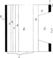
基体12はいかなる寸法でもよく、その具体的な寸法は用途により決まる。適切な直径には、それらに限定はされないが、2インチ(50mm)、4インチ(100mm)、6インチ(150mm)および8インチ(200mm)が含まれる。いくつかの実施態様において、シリコン基体12は比較的厚く、例えば、250ミクロンよりも大きい。厚い基体は、いくつかの場合において、薄い基体に起こり得る曲げに一般に抵抗できる。いくつかの実施態様において、シリコン基体12は、シリコン基体を通したビア24の形成を容易にするために、好ましくは薄く、例えば、100ミクロン未満である。
本明細書で用いたとき、「電気コンタクト」もしくは「コンタクト」という語句は、電極、端子、コンタクトパッド、コンタクト区域、コンタクト領域などを含む電源により有効にコンタクトできる半導体デバイス上のいかなる伝導構造物をもいう。バックサイドコンタクト20およびトップサイドコンタクト16は、いくつかの金属を含む伝導性材料で形成される。当業界で既知の適切な伝導性材料のいずれを用いてもよい。コンタクト16、20の組成は、コンタクトの型によるかもしれない。例えば、コンタクト16、20は、n‐型材料もしくはp‐型材料に接触し得る。n‐型コンタクトに適する金属には、チタン、ニッケル、アルミニウム、金、銅およびこれらの合金が含まれる。p‐型コンタクトに適する金属には、ニッケル、金およびチタン、ならびにこれらの合金が含まれる。
Claims (10)
- 基体のバックサイドから延びる少なくとも1つのビアを有するシリコン基体;
前記ビア中に形成される電気コンタクト;
前記基体上に形成される窒化ガリウム材料領域、ここで、前記窒化ガリウム材料領域は1より多い窒化ガリウム材料層を含む;および
前記基体と前記窒化ガリウム材料領域との間に形成され、窒化ガリウムの合金を含む非伝導層
を含む半導体構造物であって、
半導体構造物がFETを含み、前記電気コンタクトおよびビアが前記基体のバックサイドから前記窒化ガリウム材料領域内に形成されるソース領域まで延び、
前記ビアが前記窒化ガリウム材料領域の全ての層を通して延びていない、
半導体構造物。 - 前記電気コンタクトが前記基体のバックサイドから前記半導体構造物の伝導領域まで延びる、請求項1に記載の半導体構造物。
- 前記電気コンタクトが前記基体のバックサイドから前記窒化ガリウム材料領域まで延びる、請求項2に記載の半導体構造物。
- 前記ビアが前記非伝導層を通して形成され、前記電気コンタクトが前記非伝導層を通して延びる、請求項1に記載の半導体構造物。
- 前記非伝導層が組成的に勾配をつけた遷移層を含む、請求項1に記載の半導体構造物。
- 前記ビアが前記基体を通して形成され、前記電気コンタクトが前記基体を通して延びる、請求項1に記載の半導体構造物。
- 前記電気コンタクトが前記基体のバックサイドから前記窒化ガリウム材料領域内の領域まで延びる、請求項1に記載の半導体構造物。
- さらに前記半導体構造物のトップサイド上に形成されるトップサイド電気コンタクトを含む、請求項1に記載の半導体構造物。
- 前記半導体構造物が垂直伝導が可能である、請求項1に記載の半導体構造物。
- 半導体デバイスが前記窒化ガリウム材料領域中に形成される、請求項1に記載の半導体構造物。
Applications Claiming Priority (3)
| Application Number | Priority Date | Filing Date | Title |
|---|---|---|---|
| US09/792,414 | 2001-02-23 | ||
| US09/792,414 US6611002B2 (en) | 2001-02-23 | 2001-02-23 | Gallium nitride material devices and methods including backside vias |
| PCT/US2002/005182 WO2002069410A2 (en) | 2001-02-23 | 2002-02-22 | Gallium nitride material devices including backside vias and methods of fabrication |
Publications (3)
| Publication Number | Publication Date |
|---|---|
| JP2004530289A JP2004530289A (ja) | 2004-09-30 |
| JP2004530289A5 JP2004530289A5 (ja) | 2005-12-22 |
| JP4792558B2 true JP4792558B2 (ja) | 2011-10-12 |
Family
ID=25156813
Family Applications (1)
| Application Number | Title | Priority Date | Filing Date |
|---|---|---|---|
| JP2002568431A Expired - Lifetime JP4792558B2 (ja) | 2001-02-23 | 2002-02-22 | バックサイドビアを含む窒化ガリウム材料デバイスおよび方法 |
Country Status (6)
| Country | Link |
|---|---|
| US (1) | US6611002B2 (ja) |
| EP (3) | EP3561883A1 (ja) |
| JP (1) | JP4792558B2 (ja) |
| AU (1) | AU2002252047A1 (ja) |
| TW (1) | TW530327B (ja) |
| WO (1) | WO2002069410A2 (ja) |
Families Citing this family (161)
| Publication number | Priority date | Publication date | Assignee | Title |
|---|---|---|---|---|
| US7687888B2 (en) | 2000-08-04 | 2010-03-30 | The Regents Of The University Of California | Method of controlling stress in gallium nitride films deposited on substrates |
| US6649287B2 (en) * | 2000-12-14 | 2003-11-18 | Nitronex Corporation | Gallium nitride materials and methods |
| US6657237B2 (en) * | 2000-12-18 | 2003-12-02 | Samsung Electro-Mechanics Co., Ltd. | GaN based group III-V nitride semiconductor light-emitting diode and method for fabricating the same |
| US7233028B2 (en) * | 2001-02-23 | 2007-06-19 | Nitronex Corporation | Gallium nitride material devices and methods of forming the same |
| US6956250B2 (en) * | 2001-02-23 | 2005-10-18 | Nitronex Corporation | Gallium nitride materials including thermally conductive regions |
| DE10111501B4 (de) | 2001-03-09 | 2019-03-21 | Osram Opto Semiconductors Gmbh | Strahlungsemittierendes Halbleiterbauelement und Verfahren zu dessen Herstellung |
| US7067849B2 (en) * | 2001-07-17 | 2006-06-27 | Lg Electronics Inc. | Diode having high brightness and method thereof |
| JP2003086839A (ja) * | 2001-09-07 | 2003-03-20 | Sharp Corp | 窒化物半導体発光素子およびその製造方法 |
| US6949395B2 (en) * | 2001-10-22 | 2005-09-27 | Oriol, Inc. | Method of making diode having reflective layer |
| US7148520B2 (en) | 2001-10-26 | 2006-12-12 | Lg Electronics Inc. | Diode having vertical structure and method of manufacturing the same |
| US6900501B2 (en) * | 2001-11-02 | 2005-05-31 | Cree Microwave, Inc. | Silicon on insulator device with improved heat removal |
| US20030132433A1 (en) * | 2002-01-15 | 2003-07-17 | Piner Edwin L. | Semiconductor structures including a gallium nitride material component and a silicon germanium component |
| TW561637B (en) * | 2002-10-16 | 2003-11-11 | Epistar Corp | LED having contact layer with dual dopant state |
| US6927422B2 (en) * | 2002-10-17 | 2005-08-09 | Astralux, Inc. | Double heterojunction light emitting diodes and laser diodes having quantum dot silicon light emitters |
| DE10250832B4 (de) * | 2002-10-31 | 2010-02-11 | Infineon Technologies Ag | MOS-Transistor auf SOI-Substrat mit Source-Durchkontaktierung und Verfahren zur Herstellung eines solchen Transistors |
| US6977396B2 (en) * | 2003-02-19 | 2005-12-20 | Lumileds Lighting U.S., Llc | High-powered light emitting device with improved thermal properties |
| US7714345B2 (en) * | 2003-04-30 | 2010-05-11 | Cree, Inc. | Light-emitting devices having coplanar electrical contacts adjacent to a substrate surface opposite an active region and methods of forming the same |
| WO2005060007A1 (en) * | 2003-08-05 | 2005-06-30 | Nitronex Corporation | Gallium nitride material transistors and methods associated with the same |
| WO2005029573A1 (en) * | 2003-09-19 | 2005-03-31 | Tinggi Technologies Private Limited | Fabrication of semiconductor devices |
| US7071498B2 (en) * | 2003-12-17 | 2006-07-04 | Nitronex Corporation | Gallium nitride material devices including an electrode-defining layer and methods of forming the same |
| US20050145851A1 (en) * | 2003-12-17 | 2005-07-07 | Nitronex Corporation | Gallium nitride material structures including isolation regions and methods |
| KR101228428B1 (ko) * | 2004-02-20 | 2013-01-31 | 오스람 옵토 세미컨덕터스 게엠베하 | 광전 소자, 다수의 광전 소자를 구비한 장치 및 광전 소자를 제조하기 위한 방법 |
| KR20070013273A (ko) * | 2004-03-15 | 2007-01-30 | 팅기 테크놀러지스 프라이빗 리미티드 | 반도체 장치의 제조 |
| EP1756875A4 (en) | 2004-04-07 | 2010-12-29 | Tinggi Technologies Private Ltd | FABRICATION OF A RETROFLECTIVE LAYER ON SEMICONDUCTOR ELECTROLUMINESCENT DIODES |
| US7361946B2 (en) * | 2004-06-28 | 2008-04-22 | Nitronex Corporation | Semiconductor device-based sensors |
| US7339205B2 (en) | 2004-06-28 | 2008-03-04 | Nitronex Corporation | Gallium nitride materials and methods associated with the same |
| US7687827B2 (en) * | 2004-07-07 | 2010-03-30 | Nitronex Corporation | III-nitride materials including low dislocation densities and methods associated with the same |
| US6928878B1 (en) | 2004-09-28 | 2005-08-16 | Rosemount Aerospace Inc. | Pressure sensor |
| DE102004061865A1 (de) | 2004-09-29 | 2006-03-30 | Osram Opto Semiconductors Gmbh | Verfahren zur Herstellung eines Dünnfilmhalbleiterchips |
| US20060214289A1 (en) * | 2004-10-28 | 2006-09-28 | Nitronex Corporation | Gallium nitride material-based monolithic microwave integrated circuits |
| KR100728533B1 (ko) * | 2004-11-23 | 2007-06-15 | 삼성코닝 주식회사 | 질화갈륨 단결정 후막 및 이의 제조방법 |
| US7247889B2 (en) | 2004-12-03 | 2007-07-24 | Nitronex Corporation | III-nitride material structures including silicon substrates |
| US7436039B2 (en) * | 2005-01-06 | 2008-10-14 | Velox Semiconductor Corporation | Gallium nitride semiconductor device |
| JP4802542B2 (ja) * | 2005-04-19 | 2011-10-26 | 株式会社デンソー | 炭化珪素半導体装置 |
| US7365374B2 (en) * | 2005-05-03 | 2008-04-29 | Nitronex Corporation | Gallium nitride material structures including substrates and methods associated with the same |
| US9331192B2 (en) | 2005-06-29 | 2016-05-03 | Cree, Inc. | Low dislocation density group III nitride layers on silicon carbide substrates and methods of making the same |
| SG130975A1 (en) * | 2005-09-29 | 2007-04-26 | Tinggi Tech Private Ltd | Fabrication of semiconductor devices for light emission |
| US20070202360A1 (en) * | 2005-10-04 | 2007-08-30 | Nitronex Corporation | Gallium nitride material transistors and methods for wideband applications |
| SG131803A1 (en) * | 2005-10-19 | 2007-05-28 | Tinggi Tech Private Ltd | Fabrication of transistors |
| WO2007064689A1 (en) * | 2005-12-02 | 2007-06-07 | Nitronex Corporation | Gallium nitride material devices and associated methods |
| US7566913B2 (en) | 2005-12-02 | 2009-07-28 | Nitronex Corporation | Gallium nitride material devices including conductive regions and methods associated with the same |
| SG133432A1 (en) * | 2005-12-20 | 2007-07-30 | Tinggi Tech Private Ltd | Localized annealing during semiconductor device fabrication |
| WO2007081964A2 (en) | 2006-01-10 | 2007-07-19 | Cree, Inc. | Silicon carbide dimpled substrate |
| US7476606B2 (en) * | 2006-03-28 | 2009-01-13 | Northrop Grumman Corporation | Eutectic bonding of ultrathin semiconductors |
| US20100269819A1 (en) * | 2006-08-14 | 2010-10-28 | Sievers Robert E | Human Powered Dry Powder Inhaler and Dry Powder Inhaler Compositions |
| SG140473A1 (en) | 2006-08-16 | 2008-03-28 | Tinggi Tech Private Ltd | Improvements in external light efficiency of light emitting diodes |
| SG140512A1 (en) * | 2006-09-04 | 2008-03-28 | Tinggi Tech Private Ltd | Electrical current distribution in light emitting devices |
| JP5091445B2 (ja) * | 2006-09-15 | 2012-12-05 | 株式会社東芝 | 半導体装置およびその製造方法 |
| US7834367B2 (en) * | 2007-01-19 | 2010-11-16 | Cree, Inc. | Low voltage diode with reduced parasitic resistance and method for fabricating |
| DE102007003282B4 (de) * | 2007-01-23 | 2023-12-21 | OSRAM Opto Semiconductors Gesellschaft mit beschränkter Haftung | Leuchtdiodenchip |
| CN101244533B (zh) * | 2007-02-16 | 2010-09-15 | 香港应用科技研究院有限公司 | 超平坦化学机械抛光技术之方法及使用该方法制造的半导体组件 |
| US8188459B2 (en) * | 2007-04-12 | 2012-05-29 | Massachusetts Institute Of Technology | Devices based on SI/nitride structures |
| WO2008128160A1 (en) * | 2007-04-12 | 2008-10-23 | Massachusetts Institute Of Technology | Hemts based on si/nitride structures |
| CN100580905C (zh) * | 2007-04-20 | 2010-01-13 | 晶能光电(江西)有限公司 | 获得在分割衬底上制造的半导体器件的高质量边界的方法 |
| DE102007022947B4 (de) | 2007-04-26 | 2022-05-05 | OSRAM Opto Semiconductors Gesellschaft mit beschränkter Haftung | Optoelektronischer Halbleiterkörper und Verfahren zur Herstellung eines solchen |
| US8846457B2 (en) | 2007-05-31 | 2014-09-30 | Nthdegree Technologies Worldwide Inc | Printable composition of a liquid or gel suspension of diodes |
| US9534772B2 (en) | 2007-05-31 | 2017-01-03 | Nthdegree Technologies Worldwide Inc | Apparatus with light emitting diodes |
| US8674593B2 (en) | 2007-05-31 | 2014-03-18 | Nthdegree Technologies Worldwide Inc | Diode for a printable composition |
| US9419179B2 (en) | 2007-05-31 | 2016-08-16 | Nthdegree Technologies Worldwide Inc | Diode for a printable composition |
| US9425357B2 (en) | 2007-05-31 | 2016-08-23 | Nthdegree Technologies Worldwide Inc. | Diode for a printable composition |
| US8384630B2 (en) | 2007-05-31 | 2013-02-26 | Nthdegree Technologies Worldwide Inc | Light emitting, photovoltaic or other electronic apparatus and system |
| US9018833B2 (en) | 2007-05-31 | 2015-04-28 | Nthdegree Technologies Worldwide Inc | Apparatus with light emitting or absorbing diodes |
| US8809126B2 (en) | 2007-05-31 | 2014-08-19 | Nthdegree Technologies Worldwide Inc | Printable composition of a liquid or gel suspension of diodes |
| US8415879B2 (en) | 2007-05-31 | 2013-04-09 | Nthdegree Technologies Worldwide Inc | Diode for a printable composition |
| US8877101B2 (en) | 2007-05-31 | 2014-11-04 | Nthdegree Technologies Worldwide Inc | Method of manufacturing a light emitting, power generating or other electronic apparatus |
| US8852467B2 (en) | 2007-05-31 | 2014-10-07 | Nthdegree Technologies Worldwide Inc | Method of manufacturing a printable composition of a liquid or gel suspension of diodes |
| US9343593B2 (en) | 2007-05-31 | 2016-05-17 | Nthdegree Technologies Worldwide Inc | Printable composition of a liquid or gel suspension of diodes |
| US7745848B1 (en) | 2007-08-15 | 2010-06-29 | Nitronex Corporation | Gallium nitride material devices and thermal designs thereof |
| JP2009054659A (ja) * | 2007-08-24 | 2009-03-12 | Fuji Electric Device Technology Co Ltd | 窒化ガリウム半導体装置の製造方法 |
| DE102007057756B4 (de) * | 2007-11-30 | 2022-03-10 | OSRAM Opto Semiconductors Gesellschaft mit beschränkter Haftung | Verfahren zur Herstellung eines optoelektronischen Halbleiterkörpers |
| FR2924533B1 (fr) * | 2007-12-04 | 2010-08-20 | Thales Sa | Diode schottky pour application forte puissance et procede de fabrication |
| US7985979B2 (en) | 2007-12-19 | 2011-07-26 | Koninklijke Philips Electronics, N.V. | Semiconductor light emitting device with light extraction structures |
| JP2009182217A (ja) * | 2008-01-31 | 2009-08-13 | Sumitomo Electric Ind Ltd | 半導体装置およびその製造方法 |
| US8026581B2 (en) * | 2008-02-05 | 2011-09-27 | International Rectifier Corporation | Gallium nitride material devices including diamond regions and methods associated with the same |
| JP2009200343A (ja) * | 2008-02-22 | 2009-09-03 | Sumitomo Electric Ind Ltd | ダイヤモンド電子素子 |
| US8343824B2 (en) * | 2008-04-29 | 2013-01-01 | International Rectifier Corporation | Gallium nitride material processing and related device structures |
| US7992332B2 (en) | 2008-05-13 | 2011-08-09 | Nthdegree Technologies Worldwide Inc. | Apparatuses for providing power for illumination of a display object |
| US8127477B2 (en) | 2008-05-13 | 2012-03-06 | Nthdegree Technologies Worldwide Inc | Illuminating display systems |
| KR100981275B1 (ko) * | 2008-09-25 | 2010-09-10 | 주식회사 에피밸리 | 3족 질화물 반도체 발광소자 |
| KR101064053B1 (ko) * | 2009-02-25 | 2011-09-08 | 엘지이노텍 주식회사 | 발광소자 및 그 제조방법 |
| CN102341926A (zh) * | 2009-03-05 | 2012-02-01 | 株式会社小糸制作所 | 发光模块、发光模块的制造方法及灯具单元 |
| DE102009023849B4 (de) * | 2009-06-04 | 2022-10-20 | OSRAM Opto Semiconductors Gesellschaft mit beschränkter Haftung | Optoelektronischer Halbleiterkörper und optoelektronischer Halbleiterchip |
| JP2010283124A (ja) * | 2009-06-04 | 2010-12-16 | Disco Abrasive Syst Ltd | 発光ダイオード |
| JP5487749B2 (ja) * | 2009-06-17 | 2014-05-07 | 富士通株式会社 | 半導体装置及びその製造方法 |
| KR20120055705A (ko) * | 2009-08-19 | 2012-05-31 | 더 리전츠 오브 더 유니버시티 오브 캘리포니아 | (Ga, Al, In, B)N 레이저 다이오드에서의 선택적 식각을 위한 구조물 및 방법 |
| DE102009047881B4 (de) | 2009-09-30 | 2022-03-03 | OSRAM Opto Semiconductors Gesellschaft mit beschränkter Haftung | Verfahren zur Herstellung einer epitaktisch hergestellten Schichtstruktur |
| KR101007077B1 (ko) * | 2009-11-06 | 2011-01-10 | 엘지이노텍 주식회사 | 발광소자, 발광소자 패키지 및 그 제조방법 |
| KR101662037B1 (ko) * | 2009-12-02 | 2016-10-05 | 삼성전자 주식회사 | 발광 소자 및 그 제조 방법 |
| US9299664B2 (en) * | 2010-01-18 | 2016-03-29 | Semiconductor Components Industries, Llc | Method of forming an EM protected semiconductor die |
| US20110198609A1 (en) * | 2010-02-12 | 2011-08-18 | Taiwan Semiconductor Manufacturing Company, Ltd. | Light-Emitting Devices with Through-Substrate Via Connections |
| US8604498B2 (en) | 2010-03-26 | 2013-12-10 | Tsmc Solid State Lighting Ltd. | Single phosphor layer photonic device for generating white light or color lights |
| DE112011101156T5 (de) * | 2010-04-01 | 2013-01-24 | Panasonic Corporation | Leuchtdiodenelement und Leuchtdiodenvorrichtung |
| SG185547A1 (en) | 2010-05-18 | 2012-12-28 | Agency Science Tech & Res | Method of forming a light emitting diode structure and a light emitting diode structure |
| US8772832B2 (en) * | 2010-06-04 | 2014-07-08 | Hrl Laboratories, Llc | GaN HEMTs with a back gate connected to the source |
| JP4657374B1 (ja) * | 2010-06-16 | 2011-03-23 | 有限会社ナプラ | 発光ダイオード、発光装置、照明装置及びディスプレイ |
| KR101761385B1 (ko) | 2010-07-12 | 2017-08-04 | 엘지이노텍 주식회사 | 발광 소자 |
| CN103633222B (zh) * | 2010-09-01 | 2017-08-11 | 无限科技全球公司 | 二极体、二极体或其他二端积体电路的液体或胶体悬浮液的可印组成物及其制备方法 |
| EP2618369B1 (en) * | 2010-09-01 | 2020-11-11 | Nthdegree Technologies Worldwide Inc. | Diodes, printable compositions of a liquid or gel suspension of diodes or other two-terminal integrated circuits, and methods of making same |
| WO2012031096A2 (en) * | 2010-09-01 | 2012-03-08 | Nthdegree Technologies Worldwide Inc. | Light emitting, power generating or other electronic apparatus and method of manufacturing same |
| CN102054913B (zh) | 2010-11-09 | 2013-07-10 | 映瑞光电科技(上海)有限公司 | 发光二极管及其制造方法、发光装置 |
| CN102054914B (zh) | 2010-11-09 | 2013-09-04 | 映瑞光电科技(上海)有限公司 | 发光二极管及其制造方法、发光装置 |
| KR20130126948A (ko) | 2010-12-15 | 2013-11-21 | 이피션트 파워 컨버젼 코퍼레이션 | 후면 격리를 갖는 반도체 소자 |
| US20120274366A1 (en) | 2011-04-28 | 2012-11-01 | International Rectifier Corporation | Integrated Power Stage |
| JP5887638B2 (ja) * | 2011-05-30 | 2016-03-16 | 億光電子工業股▲ふん▼有限公司Everlight Electronics Co.,Ltd. | 発光ダイオード |
| WO2013005372A1 (ja) * | 2011-07-01 | 2013-01-10 | パナソニック株式会社 | 半導体装置 |
| US8304916B1 (en) * | 2011-07-06 | 2012-11-06 | Northrop Grumman Systems Corporation | Half-through vias for suppression of substrate modes |
| US8618647B2 (en) * | 2011-08-01 | 2013-12-31 | Tessera, Inc. | Packaged microelectronic elements having blind vias for heat dissipation |
| US8664679B2 (en) | 2011-09-29 | 2014-03-04 | Toshiba Techno Center Inc. | Light emitting devices having light coupling layers with recessed electrodes |
| US20130082274A1 (en) | 2011-09-29 | 2013-04-04 | Bridgelux, Inc. | Light emitting devices having dislocation density maintaining buffer layers |
| US9012921B2 (en) | 2011-09-29 | 2015-04-21 | Kabushiki Kaisha Toshiba | Light emitting devices having light coupling layers |
| US9178114B2 (en) | 2011-09-29 | 2015-11-03 | Manutius Ip, Inc. | P-type doping layers for use with light emitting devices |
| US8853668B2 (en) | 2011-09-29 | 2014-10-07 | Kabushiki Kaisha Toshiba | Light emitting regions for use with light emitting devices |
| US8698163B2 (en) | 2011-09-29 | 2014-04-15 | Toshiba Techno Center Inc. | P-type doping layers for use with light emitting devices |
| US8778788B2 (en) | 2011-10-11 | 2014-07-15 | Avogy, Inc. | Method of fabricating a gallium nitride merged P-i-N Schottky (MPS) diode |
| US9224828B2 (en) | 2011-10-11 | 2015-12-29 | Avogy, Inc. | Method and system for floating guard rings in gallium nitride materials |
| US8749015B2 (en) | 2011-11-17 | 2014-06-10 | Avogy, Inc. | Method and system for fabricating floating guard rings in GaN materials |
| KR20130104612A (ko) * | 2012-03-14 | 2013-09-25 | 서울바이오시스 주식회사 | 발광 다이오드 및 그것을 제조하는 방법 |
| JP5943828B2 (ja) * | 2012-03-28 | 2016-07-05 | 有限会社 ナプラ | 発光デバイス、照明装置、ディスプレイ及び信号灯 |
| KR101979944B1 (ko) | 2012-10-18 | 2019-05-17 | 엘지이노텍 주식회사 | 발광소자 |
| KR101988893B1 (ko) * | 2012-12-12 | 2019-09-30 | 한국전자통신연구원 | 반도체 소자 및 이를 제조하는 방법 |
| US9105621B2 (en) * | 2012-12-20 | 2015-08-11 | Imec | Method for bonding of group III-nitride device-on-silicon and devices obtained thereof |
| KR101504331B1 (ko) | 2013-03-04 | 2015-03-19 | 삼성전자주식회사 | 발광소자 패키지 |
| US9773884B2 (en) | 2013-03-15 | 2017-09-26 | Hrl Laboratories, Llc | III-nitride transistor with engineered substrate |
| US9184243B2 (en) | 2013-07-12 | 2015-11-10 | Infineon Technologies Americas Corp. | Monolithic composite III-nitride transistor with high voltage group IV enable switch |
| TWI536605B (zh) * | 2013-08-20 | 2016-06-01 | 隆達電子股份有限公司 | 發光二極體 |
| US20150162832A1 (en) | 2013-12-09 | 2015-06-11 | International Rectifier Corporation | Group III-V Voltage Converter with Monolithically Integrated Level Shifter, High Side Driver, and High Side Power Switch |
| US20150270356A1 (en) * | 2014-03-20 | 2015-09-24 | Massachusetts Institute Of Technology | Vertical nitride semiconductor device |
| US10312731B2 (en) | 2014-04-24 | 2019-06-04 | Westrock Shared Services, Llc | Powered shelf system for inductively powering electrical components of consumer product packages |
| DE102014114194B4 (de) | 2014-09-30 | 2023-10-19 | OSRAM Opto Semiconductors Gesellschaft mit beschränkter Haftung | Optoelektronischer Halbleiterchip und Verfahren zu dessen Herstellung |
| US9419120B2 (en) | 2014-11-05 | 2016-08-16 | Northrop Grumman Systems Corporation | Multichannel devices with improved performance |
| US10075132B2 (en) | 2015-03-24 | 2018-09-11 | Nxp Usa, Inc. | RF amplifier with conductor-less region underlying filter circuit inductor, and methods of manufacture thereof |
| US9509251B2 (en) | 2015-03-24 | 2016-11-29 | Freescale Semiconductor, Inc. | RF amplifier module and methods of manufacture thereof |
| US9871107B2 (en) | 2015-05-22 | 2018-01-16 | Nxp Usa, Inc. | Device with a conductive feature formed over a cavity and method therefor |
| WO2016200882A1 (en) * | 2015-06-08 | 2016-12-15 | Corning Incorporated | Microled display without transfer |
| KR102554702B1 (ko) * | 2015-08-25 | 2023-07-13 | 쑤저우 레킨 세미컨덕터 컴퍼니 리미티드 | 발광소자 및 이를 포함하는 발광소자 패키지 |
| US9673281B2 (en) | 2015-09-08 | 2017-06-06 | Macom Technology Solutions Holdings, Inc. | Parasitic channel mitigation using rare-earth oxide and/or rare-earth nitride diffusion barrier regions |
| US9704705B2 (en) | 2015-09-08 | 2017-07-11 | Macom Technology Solutions Holdings, Inc. | Parasitic channel mitigation via reaction with active species |
| US9627473B2 (en) | 2015-09-08 | 2017-04-18 | Macom Technology Solutions Holdings, Inc. | Parasitic channel mitigation in III-nitride material semiconductor structures |
| US20170069721A1 (en) | 2015-09-08 | 2017-03-09 | M/A-Com Technology Solutions Holdings, Inc. | Parasitic channel mitigation using silicon carbide diffusion barrier regions |
| US9806182B2 (en) | 2015-09-08 | 2017-10-31 | Macom Technology Solutions Holdings, Inc. | Parasitic channel mitigation using elemental diboride diffusion barrier regions |
| US9773898B2 (en) | 2015-09-08 | 2017-09-26 | Macom Technology Solutions Holdings, Inc. | III-nitride semiconductor structures comprising spatially patterned implanted species |
| US10211294B2 (en) | 2015-09-08 | 2019-02-19 | Macom Technology Solutions Holdings, Inc. | III-nitride semiconductor structures comprising low atomic mass species |
| US9799520B2 (en) | 2015-09-08 | 2017-10-24 | Macom Technology Solutions Holdings, Inc. | Parasitic channel mitigation via back side implantation |
| US9787254B2 (en) | 2015-09-23 | 2017-10-10 | Nxp Usa, Inc. | Encapsulated semiconductor device package with heatsink opening, and methods of manufacture thereof |
| CN106910724B (zh) * | 2016-04-05 | 2020-06-05 | 苏州捷芯威半导体有限公司 | 一种半导体器件 |
| US10217827B2 (en) * | 2016-05-11 | 2019-02-26 | Rfhic Corporation | High electron mobility transistor (HEMT) |
| US9960127B2 (en) | 2016-05-18 | 2018-05-01 | Macom Technology Solutions Holdings, Inc. | High-power amplifier package |
| EP3471154A4 (en) * | 2016-06-10 | 2019-06-05 | LG Innotek Co., Ltd. | SEMICONDUCTOR DEVICE |
| US10134658B2 (en) | 2016-08-10 | 2018-11-20 | Macom Technology Solutions Holdings, Inc. | High power transistors |
| US10096550B2 (en) | 2017-02-21 | 2018-10-09 | Raytheon Company | Nitride structure having gold-free contact and methods for forming such structures |
| US10224285B2 (en) | 2017-02-21 | 2019-03-05 | Raytheon Company | Nitride structure having gold-free contact and methods for forming such structures |
| US10128377B2 (en) | 2017-02-24 | 2018-11-13 | International Business Machines Corporation | Independent gate FinFET with backside gate contact |
| US11038023B2 (en) | 2018-07-19 | 2021-06-15 | Macom Technology Solutions Holdings, Inc. | III-nitride material semiconductor structures on conductive silicon substrates |
| DE102018121672A1 (de) * | 2018-09-05 | 2020-03-05 | Technische Universität Darmstadt | Gunndiode und Verfahren zum Erzeugen einer Terahertzstrahlung |
| DE102018131404A1 (de) * | 2018-12-07 | 2020-06-10 | Osram Opto Semiconductors Gmbh | Optoelektronisches halbleiterbauteil und verfahren zur herstellung von optoelektronischen halbleiterbauteilen |
| US20220085197A1 (en) * | 2019-02-19 | 2022-03-17 | Mitsubishi Electric Corporation | Semiconductor device, and method of manufacturing semiconductor device |
| TWI683370B (zh) * | 2019-03-12 | 2020-01-21 | 環球晶圓股份有限公司 | 半導體元件及其製造方法 |
| US11411099B2 (en) | 2019-05-28 | 2022-08-09 | Glc Semiconductor Group (Cq) Co., Ltd. | Semiconductor device |
| TWI717745B (zh) * | 2019-05-28 | 2021-02-01 | 大陸商聚力成半導體(重慶)有限公司 | 半導體裝置 |
| DE102019125847A1 (de) * | 2019-09-25 | 2021-03-25 | Technische Universität Darmstadt | Gunndiode und Verfahren zu deren Herstellung |
| US11270928B2 (en) * | 2020-04-02 | 2022-03-08 | Macom Technology Solutions Holdings, Inc. | Unibody lateral via |
Citations (14)
| Publication number | Priority date | Publication date | Assignee | Title |
|---|---|---|---|---|
| JPS5879773A (ja) * | 1981-11-06 | 1983-05-13 | Fujitsu Ltd | 電界効果トランジスタ |
| JPH01149461A (ja) * | 1987-12-04 | 1989-06-12 | Nec Corp | 半導体装置 |
| JPH06151473A (ja) * | 1992-11-09 | 1994-05-31 | Oki Electric Ind Co Ltd | 化合物半導体素子およびその製造方法 |
| JPH09326534A (ja) * | 1996-06-04 | 1997-12-16 | Fuji Electric Co Ltd | Iii 族窒化物半導体装置 |
| JPH10114600A (ja) * | 1996-05-31 | 1998-05-06 | Sumitomo Electric Ind Ltd | 発光素子および発光素子用ウエハならびにその製造方法 |
| JPH10242584A (ja) * | 1997-02-28 | 1998-09-11 | Hitachi Ltd | 半導体発光素子 |
| JPH10308560A (ja) * | 1997-05-08 | 1998-11-17 | Toshiba Corp | 半導体発光素子および発光装置 |
| JPH1145892A (ja) * | 1997-05-28 | 1999-02-16 | Sony Corp | 半導体装置およびその製造方法 |
| JPH1187526A (ja) * | 1997-06-25 | 1999-03-30 | Commiss Energ Atom | マイクロエレクトロニクス素子とエッチング困難な半導体材料と金属化された孔とを備えた構造 |
| JP2000036618A (ja) * | 1998-07-21 | 2000-02-02 | Murata Mfg Co Ltd | 半導体発光素子及びZnO膜の形成方法 |
| JP2000114275A (ja) * | 1998-10-05 | 2000-04-21 | Nec Corp | 電界効果トランジスタおよびその製造方法 |
| JP2000133842A (ja) * | 1998-10-22 | 2000-05-12 | Sanyo Electric Co Ltd | 半導体素子及びその製造方法 |
| JP2000261035A (ja) * | 1999-03-12 | 2000-09-22 | Toyoda Gosei Co Ltd | GaN系の半導体素子 |
| JP2000277441A (ja) * | 1999-03-26 | 2000-10-06 | Nagoya Kogyo Univ | 半導体構造とそれを備えた半導体素子及び結晶成長方法 |
Family Cites Families (38)
| Publication number | Priority date | Publication date | Assignee | Title |
|---|---|---|---|---|
| DE3718684A1 (de) * | 1987-06-04 | 1988-12-22 | Licentia Gmbh | Halbleiterkoerper |
| US4985742A (en) * | 1989-07-07 | 1991-01-15 | University Of Colorado Foundation, Inc. | High temperature semiconductor devices having at least one gallium nitride layer |
| US5192987A (en) | 1991-05-17 | 1993-03-09 | Apa Optics, Inc. | High electron mobility transistor with GaN/Alx Ga1-x N heterojunctions |
| JP3352712B2 (ja) | 1991-12-18 | 2002-12-03 | 浩 天野 | 窒化ガリウム系半導体素子及びその製造方法 |
| JPH06310547A (ja) | 1993-02-25 | 1994-11-04 | Mitsubishi Electric Corp | 半導体装置及びその製造方法 |
| US5393993A (en) | 1993-12-13 | 1995-02-28 | Cree Research, Inc. | Buffer structure between silicon carbide and gallium nitride and resulting semiconductor devices |
| JP3753747B2 (ja) * | 1993-12-27 | 2006-03-08 | 豊田合成株式会社 | 窒化ガリウム系化合物半導体レーザダイオード |
| US5523589A (en) | 1994-09-20 | 1996-06-04 | Cree Research, Inc. | Vertical geometry light emitting diode with group III nitride active layer and extended lifetime |
| US5592501A (en) | 1994-09-20 | 1997-01-07 | Cree Research, Inc. | Low-strain laser structures with group III nitride active layers |
| JP3557011B2 (ja) | 1995-03-30 | 2004-08-25 | 株式会社東芝 | 半導体発光素子、及びその製造方法 |
| JPH08307001A (ja) | 1995-04-28 | 1996-11-22 | Mitsubishi Electric Corp | 半導体レ−ザダイオ−ドおよびその製造方法 |
| US5739554A (en) | 1995-05-08 | 1998-04-14 | Cree Research, Inc. | Double heterojunction light emitting diode with gallium nitride active layer |
| JP3830051B2 (ja) | 1995-09-18 | 2006-10-04 | 株式会社 日立製作所 | 窒化物半導体基板の製造方法、窒化物半導体基板、光半導体装置の製造方法および光半導体装置 |
| JP3396356B2 (ja) | 1995-12-11 | 2003-04-14 | 三菱電機株式会社 | 半導体装置,及びその製造方法 |
| US5874747A (en) * | 1996-02-05 | 1999-02-23 | Advanced Technology Materials, Inc. | High brightness electroluminescent device emitting in the green to ultraviolet spectrum and method of making the same |
| US5905275A (en) * | 1996-06-17 | 1999-05-18 | Kabushiki Kaisha Toshiba | Gallium nitride compound semiconductor light-emitting device |
| JP3179346B2 (ja) | 1996-08-27 | 2001-06-25 | 松下電子工業株式会社 | 窒化ガリウム結晶の製造方法 |
| JP3447527B2 (ja) * | 1996-09-09 | 2003-09-16 | 株式会社東芝 | 半導体発光素子およびその製造方法 |
| US6121634A (en) * | 1997-02-21 | 2000-09-19 | Kabushiki Kaisha Toshiba | Nitride semiconductor light emitting device and its manufacturing method |
| WO1998047170A1 (en) | 1997-04-11 | 1998-10-22 | Nichia Chemical Industries, Ltd. | Method of growing nitride semiconductors, nitride semiconductor substrate and nitride semiconductor device |
| US6239033B1 (en) * | 1998-05-28 | 2001-05-29 | Sony Corporation | Manufacturing method of semiconductor device |
| JPH10335637A (ja) * | 1997-05-30 | 1998-12-18 | Sony Corp | ヘテロ接合電界効果トランジスタ |
| JP4119501B2 (ja) * | 1997-07-10 | 2008-07-16 | ローム株式会社 | 半導体発光素子 |
| JP3813740B2 (ja) | 1997-07-11 | 2006-08-23 | Tdk株式会社 | 電子デバイス用基板 |
| US6201262B1 (en) | 1997-10-07 | 2001-03-13 | Cree, Inc. | Group III nitride photonic devices on silicon carbide substrates with conductive buffer interlay structure |
| JP3036495B2 (ja) | 1997-11-07 | 2000-04-24 | 豊田合成株式会社 | 窒化ガリウム系化合物半導体の製造方法 |
| US6051849A (en) | 1998-02-27 | 2000-04-18 | North Carolina State University | Gallium nitride semiconductor structures including a lateral gallium nitride layer that extends from an underlying gallium nitride layer |
| US6500257B1 (en) | 1998-04-17 | 2002-12-31 | Agilent Technologies, Inc. | Epitaxial material grown laterally within a trench and method for producing same |
| US6265289B1 (en) | 1998-06-10 | 2001-07-24 | North Carolina State University | Methods of fabricating gallium nitride semiconductor layers by lateral growth from sidewalls into trenches, and gallium nitride semiconductor structures fabricated thereby |
| US6255198B1 (en) | 1998-11-24 | 2001-07-03 | North Carolina State University | Methods of fabricating gallium nitride microelectronic layers on silicon layers and gallium nitride microelectronic structures formed thereby |
| US6177688B1 (en) | 1998-11-24 | 2001-01-23 | North Carolina State University | Pendeoepitaxial gallium nitride semiconductor layers on silcon carbide substrates |
| US6521514B1 (en) | 1999-11-17 | 2003-02-18 | North Carolina State University | Pendeoepitaxial methods of fabricating gallium nitride semiconductor layers on sapphire substrates |
| US20020069816A1 (en) | 1999-12-13 | 2002-06-13 | Thomas Gehrke | Methods of fabricating gallium nitride layers on textured silicon substrates, and gallium nitride semiconductor structures fabricated thereby |
| US6380108B1 (en) | 1999-12-21 | 2002-04-30 | North Carolina State University | Pendeoepitaxial methods of fabricating gallium nitride semiconductor layers on weak posts, and gallium nitride semiconductor structures fabricated thereby |
| US6355497B1 (en) | 2000-01-18 | 2002-03-12 | Xerox Corporation | Removable large area, low defect density films for led and laser diode growth |
| WO2001059819A1 (en) | 2000-02-09 | 2001-08-16 | North Carolina State University | Methods of fabricating gallium nitride semiconductor layers on substrates including non-gallium nitride posts, and gallium nitride semiconductor structures fabricated thereby |
| US6261929B1 (en) | 2000-02-24 | 2001-07-17 | North Carolina State University | Methods of forming a plurality of semiconductor layers using spaced trench arrays |
| FR2809534B1 (fr) * | 2000-05-26 | 2005-01-14 | Commissariat Energie Atomique | Dispositif semiconducteur a injection electronique verticale et son procede de fabrication |
-
2001
- 2001-02-23 US US09/792,414 patent/US6611002B2/en not_active Expired - Lifetime
-
2002
- 2002-02-22 TW TW091103115A patent/TW530327B/zh not_active IP Right Cessation
- 2002-02-22 WO PCT/US2002/005182 patent/WO2002069410A2/en active Application Filing
- 2002-02-22 AU AU2002252047A patent/AU2002252047A1/en not_active Abandoned
- 2002-02-22 JP JP2002568431A patent/JP4792558B2/ja not_active Expired - Lifetime
- 2002-02-22 EP EP19172826.0A patent/EP3561883A1/en not_active Withdrawn
- 2002-02-22 EP EP15154907.8A patent/EP2894679B1/en not_active Expired - Lifetime
- 2002-02-22 EP EP02721099.6A patent/EP1378012B1/en not_active Expired - Lifetime
Patent Citations (14)
| Publication number | Priority date | Publication date | Assignee | Title |
|---|---|---|---|---|
| JPS5879773A (ja) * | 1981-11-06 | 1983-05-13 | Fujitsu Ltd | 電界効果トランジスタ |
| JPH01149461A (ja) * | 1987-12-04 | 1989-06-12 | Nec Corp | 半導体装置 |
| JPH06151473A (ja) * | 1992-11-09 | 1994-05-31 | Oki Electric Ind Co Ltd | 化合物半導体素子およびその製造方法 |
| JPH10114600A (ja) * | 1996-05-31 | 1998-05-06 | Sumitomo Electric Ind Ltd | 発光素子および発光素子用ウエハならびにその製造方法 |
| JPH09326534A (ja) * | 1996-06-04 | 1997-12-16 | Fuji Electric Co Ltd | Iii 族窒化物半導体装置 |
| JPH10242584A (ja) * | 1997-02-28 | 1998-09-11 | Hitachi Ltd | 半導体発光素子 |
| JPH10308560A (ja) * | 1997-05-08 | 1998-11-17 | Toshiba Corp | 半導体発光素子および発光装置 |
| JPH1145892A (ja) * | 1997-05-28 | 1999-02-16 | Sony Corp | 半導体装置およびその製造方法 |
| JPH1187526A (ja) * | 1997-06-25 | 1999-03-30 | Commiss Energ Atom | マイクロエレクトロニクス素子とエッチング困難な半導体材料と金属化された孔とを備えた構造 |
| JP2000036618A (ja) * | 1998-07-21 | 2000-02-02 | Murata Mfg Co Ltd | 半導体発光素子及びZnO膜の形成方法 |
| JP2000114275A (ja) * | 1998-10-05 | 2000-04-21 | Nec Corp | 電界効果トランジスタおよびその製造方法 |
| JP2000133842A (ja) * | 1998-10-22 | 2000-05-12 | Sanyo Electric Co Ltd | 半導体素子及びその製造方法 |
| JP2000261035A (ja) * | 1999-03-12 | 2000-09-22 | Toyoda Gosei Co Ltd | GaN系の半導体素子 |
| JP2000277441A (ja) * | 1999-03-26 | 2000-10-06 | Nagoya Kogyo Univ | 半導体構造とそれを備えた半導体素子及び結晶成長方法 |
Also Published As
| Publication number | Publication date |
|---|---|
| TW530327B (en) | 2003-05-01 |
| US20020117681A1 (en) | 2002-08-29 |
| EP1378012A2 (en) | 2004-01-07 |
| AU2002252047A1 (en) | 2002-09-12 |
| EP2894679B1 (en) | 2019-05-08 |
| US6611002B2 (en) | 2003-08-26 |
| WO2002069410A3 (en) | 2003-03-06 |
| JP2004530289A (ja) | 2004-09-30 |
| WO2002069410A2 (en) | 2002-09-06 |
| EP3561883A1 (en) | 2019-10-30 |
| EP1378012B1 (en) | 2017-12-13 |
| EP2894679A1 (en) | 2015-07-15 |
Similar Documents
| Publication | Publication Date | Title |
|---|---|---|
| JP4792558B2 (ja) | バックサイドビアを含む窒化ガリウム材料デバイスおよび方法 | |
| US7233028B2 (en) | Gallium nitride material devices and methods of forming the same | |
| JP4311939B2 (ja) | 熱伝導性領域を含む窒化ガリウム材料 | |
| US8263985B2 (en) | Semiconductor light emitting device having one or more recesses on a layer | |
| US7566913B2 (en) | Gallium nitride material devices including conductive regions and methods associated with the same | |
| KR20060126712A (ko) | 전극 형성층을 포함하는 질화갈륨 재료 영역을 사용하는반도체 구조물, 트랜지스터 및 쇼트키 다이오드, 및 그들을형성하는 방법 | |
| JP2007067418A (ja) | 二重ヘテロ構造の発光領域を有するiii族窒化物発光デバイス | |
| US9209358B2 (en) | Semiconductor device and method of fabricating the same | |
| KR101782081B1 (ko) | 발광 소자 | |
| US8026581B2 (en) | Gallium nitride material devices including diamond regions and methods associated with the same | |
| KR101719623B1 (ko) | 발광소자 | |
| KR101072200B1 (ko) | 발광소자 및 그 제조방법 | |
| KR100762003B1 (ko) | 수직구조 질화물계 발광다이오드 소자의 제조방법 | |
| KR20090076163A (ko) | 질화물 반도체 발광소자 제조방법 및 이에 의해 제조된질화물 반도체 발광소자 | |
| KR101364718B1 (ko) | 발광 소자 및 그 제조 방법 | |
| KR101111748B1 (ko) | 수직구조 질화갈륨계 반도체 발광소자의 제조방법 | |
| TW202123487A (zh) | 發光二極體以及形成發光二極體的方法 | |
| KR102591148B1 (ko) | 비발광 3족 질화물 반도체 적층체를 제조하는 방법 | |
| KR102556721B1 (ko) | 비발광 3족 질화물 반도체 적층체 및 이를 제조하는 방법 | |
| KR102549356B1 (ko) | 비발광 3족 질화물 반도체 적층체를 제조하는 방법 | |
| KR20110132159A (ko) | 반도체 발광소자 및 그 제조방법 | |
| US10971648B2 (en) | Ultraviolet light-emitting element and light-emitting element package | |
| KR20230077839A (ko) | 비발광 3족 질화물 반도체 적층체를 제조하는 방법 | |
| KR20240118727A (ko) | 비발광 3족 질화물 반도체 적층체 | |
| KR101633814B1 (ko) | 발광 소자 |
Legal Events
| Date | Code | Title | Description |
|---|---|---|---|
| A521 | Request for written amendment filed |
Free format text: JAPANESE INTERMEDIATE CODE: A523 Effective date: 20050222 |
|
| A621 | Written request for application examination |
Free format text: JAPANESE INTERMEDIATE CODE: A621 Effective date: 20050222 |
|
| A131 | Notification of reasons for refusal |
Free format text: JAPANESE INTERMEDIATE CODE: A131 Effective date: 20081114 |
|
| A601 | Written request for extension of time |
Free format text: JAPANESE INTERMEDIATE CODE: A601 Effective date: 20090213 |
|
| A602 | Written permission of extension of time |
Free format text: JAPANESE INTERMEDIATE CODE: A602 Effective date: 20090220 |
|
| A601 | Written request for extension of time |
Free format text: JAPANESE INTERMEDIATE CODE: A601 Effective date: 20090413 |
|
| A602 | Written permission of extension of time |
Free format text: JAPANESE INTERMEDIATE CODE: A602 Effective date: 20090420 |
|
| A521 | Request for written amendment filed |
Free format text: JAPANESE INTERMEDIATE CODE: A523 Effective date: 20090514 |
|
| A131 | Notification of reasons for refusal |
Free format text: JAPANESE INTERMEDIATE CODE: A131 Effective date: 20090608 |
|
| A601 | Written request for extension of time |
Free format text: JAPANESE INTERMEDIATE CODE: A601 Effective date: 20090828 |
|
| A602 | Written permission of extension of time |
Free format text: JAPANESE INTERMEDIATE CODE: A602 Effective date: 20090904 |
|
| A521 | Request for written amendment filed |
Free format text: JAPANESE INTERMEDIATE CODE: A523 Effective date: 20091208 |
|
| A02 | Decision of refusal |
Free format text: JAPANESE INTERMEDIATE CODE: A02 Effective date: 20101108 |
|
| A521 | Request for written amendment filed |
Free format text: JAPANESE INTERMEDIATE CODE: A523 Effective date: 20110304 |
|
| A911 | Transfer to examiner for re-examination before appeal (zenchi) |
Free format text: JAPANESE INTERMEDIATE CODE: A911 Effective date: 20110331 |
|
| A711 | Notification of change in applicant |
Free format text: JAPANESE INTERMEDIATE CODE: A711 Effective date: 20110420 |
|
| TRDD | Decision of grant or rejection written | ||
| A01 | Written decision to grant a patent or to grant a registration (utility model) |
Free format text: JAPANESE INTERMEDIATE CODE: A01 Effective date: 20110506 |
|
| A521 | Request for written amendment filed |
Free format text: JAPANESE INTERMEDIATE CODE: A821 Effective date: 20110420 |
|
| A01 | Written decision to grant a patent or to grant a registration (utility model) |
Free format text: JAPANESE INTERMEDIATE CODE: A01 |
|
| A61 | First payment of annual fees (during grant procedure) |
Free format text: JAPANESE INTERMEDIATE CODE: A61 Effective date: 20110525 |
|
| A521 | Request for written amendment filed |
Free format text: JAPANESE INTERMEDIATE CODE: A523 Effective date: 20110701 |
|
| R150 | Certificate of patent or registration of utility model |
Ref document number: 4792558 Country of ref document: JP Free format text: JAPANESE INTERMEDIATE CODE: R150 Free format text: JAPANESE INTERMEDIATE CODE: R150 |
|
| FPAY | Renewal fee payment (event date is renewal date of database) |
Free format text: PAYMENT UNTIL: 20140805 Year of fee payment: 3 |
|
| R250 | Receipt of annual fees |
Free format text: JAPANESE INTERMEDIATE CODE: R250 |
|
| R250 | Receipt of annual fees |
Free format text: JAPANESE INTERMEDIATE CODE: R250 |
|
| R250 | Receipt of annual fees |
Free format text: JAPANESE INTERMEDIATE CODE: R250 |
|
| R250 | Receipt of annual fees |
Free format text: JAPANESE INTERMEDIATE CODE: R250 |
|
| R250 | Receipt of annual fees |
Free format text: JAPANESE INTERMEDIATE CODE: R250 |
|
| S533 | Written request for registration of change of name |
Free format text: JAPANESE INTERMEDIATE CODE: R313533 |
|
| R350 | Written notification of registration of transfer |
Free format text: JAPANESE INTERMEDIATE CODE: R350 |
|
| R250 | Receipt of annual fees |
Free format text: JAPANESE INTERMEDIATE CODE: R250 |
|
| R250 | Receipt of annual fees |
Free format text: JAPANESE INTERMEDIATE CODE: R250 |
|
| R250 | Receipt of annual fees |
Free format text: JAPANESE INTERMEDIATE CODE: R250 |
|
| EXPY | Cancellation because of completion of term |