JP4566325B2 - 半導体装置を製造する方法 - Google Patents
半導体装置を製造する方法 Download PDFInfo
- Publication number
- JP4566325B2 JP4566325B2 JP2000086214A JP2000086214A JP4566325B2 JP 4566325 B2 JP4566325 B2 JP 4566325B2 JP 2000086214 A JP2000086214 A JP 2000086214A JP 2000086214 A JP2000086214 A JP 2000086214A JP 4566325 B2 JP4566325 B2 JP 4566325B2
- Authority
- JP
- Japan
- Prior art keywords
- layer
- forming
- barrier layer
- conductive barrier
- opening
- Prior art date
- Legal status (The legal status is an assumption and is not a legal conclusion. Google has not performed a legal analysis and makes no representation as to the accuracy of the status listed.)
- Expired - Fee Related
Links
Images


Classifications
-
- H—ELECTRICITY
- H01—ELECTRIC ELEMENTS
- H01L—SEMICONDUCTOR DEVICES NOT COVERED BY CLASS H10
- H01L21/00—Processes or apparatus adapted for the manufacture or treatment of semiconductor or solid state devices or of parts thereof
- H01L21/70—Manufacture or treatment of devices consisting of a plurality of solid state components formed in or on a common substrate or of parts thereof; Manufacture of integrated circuit devices or of parts thereof
- H01L21/71—Manufacture of specific parts of devices defined in group H01L21/70
- H01L21/768—Applying interconnections to be used for carrying current between separate components within a device comprising conductors and dielectrics
- H01L21/76838—Applying interconnections to be used for carrying current between separate components within a device comprising conductors and dielectrics characterised by the formation and the after-treatment of the conductors
- H01L21/76841—Barrier, adhesion or liner layers
- H01L21/76843—Barrier, adhesion or liner layers formed in openings in a dielectric
- H01L21/76849—Barrier, adhesion or liner layers formed in openings in a dielectric the layer being positioned on top of the main fill metal
-
- H—ELECTRICITY
- H01—ELECTRIC ELEMENTS
- H01L—SEMICONDUCTOR DEVICES NOT COVERED BY CLASS H10
- H01L21/00—Processes or apparatus adapted for the manufacture or treatment of semiconductor or solid state devices or of parts thereof
- H01L21/70—Manufacture or treatment of devices consisting of a plurality of solid state components formed in or on a common substrate or of parts thereof; Manufacture of integrated circuit devices or of parts thereof
- H01L21/71—Manufacture of specific parts of devices defined in group H01L21/70
- H01L21/768—Applying interconnections to be used for carrying current between separate components within a device comprising conductors and dielectrics
- H01L21/76801—Applying interconnections to be used for carrying current between separate components within a device comprising conductors and dielectrics characterised by the formation and the after-treatment of the dielectrics, e.g. smoothing
- H01L21/76802—Applying interconnections to be used for carrying current between separate components within a device comprising conductors and dielectrics characterised by the formation and the after-treatment of the dielectrics, e.g. smoothing by forming openings in dielectrics
- H01L21/76807—Applying interconnections to be used for carrying current between separate components within a device comprising conductors and dielectrics characterised by the formation and the after-treatment of the dielectrics, e.g. smoothing by forming openings in dielectrics for dual damascene structures
- H01L21/76813—Applying interconnections to be used for carrying current between separate components within a device comprising conductors and dielectrics characterised by the formation and the after-treatment of the dielectrics, e.g. smoothing by forming openings in dielectrics for dual damascene structures involving a partial via etch
-
- H—ELECTRICITY
- H01—ELECTRIC ELEMENTS
- H01L—SEMICONDUCTOR DEVICES NOT COVERED BY CLASS H10
- H01L21/00—Processes or apparatus adapted for the manufacture or treatment of semiconductor or solid state devices or of parts thereof
- H01L21/70—Manufacture or treatment of devices consisting of a plurality of solid state components formed in or on a common substrate or of parts thereof; Manufacture of integrated circuit devices or of parts thereof
- H01L21/71—Manufacture of specific parts of devices defined in group H01L21/70
- H01L21/768—Applying interconnections to be used for carrying current between separate components within a device comprising conductors and dielectrics
- H01L21/76838—Applying interconnections to be used for carrying current between separate components within a device comprising conductors and dielectrics characterised by the formation and the after-treatment of the conductors
- H01L21/76841—Barrier, adhesion or liner layers
- H01L21/76843—Barrier, adhesion or liner layers formed in openings in a dielectric
-
- H—ELECTRICITY
- H01—ELECTRIC ELEMENTS
- H01L—SEMICONDUCTOR DEVICES NOT COVERED BY CLASS H10
- H01L21/00—Processes or apparatus adapted for the manufacture or treatment of semiconductor or solid state devices or of parts thereof
- H01L21/70—Manufacture or treatment of devices consisting of a plurality of solid state components formed in or on a common substrate or of parts thereof; Manufacture of integrated circuit devices or of parts thereof
- H01L21/71—Manufacture of specific parts of devices defined in group H01L21/70
- H01L21/768—Applying interconnections to be used for carrying current between separate components within a device comprising conductors and dielectrics
- H01L21/76838—Applying interconnections to be used for carrying current between separate components within a device comprising conductors and dielectrics characterised by the formation and the after-treatment of the conductors
- H01L21/76877—Filling of holes, grooves or trenches, e.g. vias, with conductive material
-
- H—ELECTRICITY
- H01—ELECTRIC ELEMENTS
- H01L—SEMICONDUCTOR DEVICES NOT COVERED BY CLASS H10
- H01L23/00—Details of semiconductor or other solid state devices
- H01L23/52—Arrangements for conducting electric current within the device in operation from one component to another, i.e. interconnections, e.g. wires, lead frames
- H01L23/522—Arrangements for conducting electric current within the device in operation from one component to another, i.e. interconnections, e.g. wires, lead frames including external interconnections consisting of a multilayer structure of conductive and insulating layers inseparably formed on the semiconductor body
- H01L23/532—Arrangements for conducting electric current within the device in operation from one component to another, i.e. interconnections, e.g. wires, lead frames including external interconnections consisting of a multilayer structure of conductive and insulating layers inseparably formed on the semiconductor body characterised by the materials
- H01L23/53204—Conductive materials
- H01L23/53209—Conductive materials based on metals, e.g. alloys, metal silicides
- H01L23/53228—Conductive materials based on metals, e.g. alloys, metal silicides the principal metal being copper
- H01L23/53233—Copper alloys
-
- H—ELECTRICITY
- H01—ELECTRIC ELEMENTS
- H01L—SEMICONDUCTOR DEVICES NOT COVERED BY CLASS H10
- H01L23/00—Details of semiconductor or other solid state devices
- H01L23/52—Arrangements for conducting electric current within the device in operation from one component to another, i.e. interconnections, e.g. wires, lead frames
- H01L23/522—Arrangements for conducting electric current within the device in operation from one component to another, i.e. interconnections, e.g. wires, lead frames including external interconnections consisting of a multilayer structure of conductive and insulating layers inseparably formed on the semiconductor body
- H01L23/532—Arrangements for conducting electric current within the device in operation from one component to another, i.e. interconnections, e.g. wires, lead frames including external interconnections consisting of a multilayer structure of conductive and insulating layers inseparably formed on the semiconductor body characterised by the materials
- H01L23/53204—Conductive materials
- H01L23/53209—Conductive materials based on metals, e.g. alloys, metal silicides
- H01L23/53228—Conductive materials based on metals, e.g. alloys, metal silicides the principal metal being copper
- H01L23/53238—Additional layers associated with copper layers, e.g. adhesion, barrier, cladding layers
-
- H—ELECTRICITY
- H01—ELECTRIC ELEMENTS
- H01L—SEMICONDUCTOR DEVICES NOT COVERED BY CLASS H10
- H01L24/00—Arrangements for connecting or disconnecting semiconductor or solid-state bodies; Methods or apparatus related thereto
- H01L24/01—Means for bonding being attached to, or being formed on, the surface to be connected, e.g. chip-to-package, die-attach, "first-level" interconnects; Manufacturing methods related thereto
- H01L24/02—Bonding areas ; Manufacturing methods related thereto
- H01L24/04—Structure, shape, material or disposition of the bonding areas prior to the connecting process
- H01L24/05—Structure, shape, material or disposition of the bonding areas prior to the connecting process of an individual bonding area
-
- H—ELECTRICITY
- H01—ELECTRIC ELEMENTS
- H01L—SEMICONDUCTOR DEVICES NOT COVERED BY CLASS H10
- H01L24/00—Arrangements for connecting or disconnecting semiconductor or solid-state bodies; Methods or apparatus related thereto
- H01L24/01—Means for bonding being attached to, or being formed on, the surface to be connected, e.g. chip-to-package, die-attach, "first-level" interconnects; Manufacturing methods related thereto
- H01L24/10—Bump connectors ; Manufacturing methods related thereto
- H01L24/11—Manufacturing methods
-
- H—ELECTRICITY
- H01—ELECTRIC ELEMENTS
- H01L—SEMICONDUCTOR DEVICES NOT COVERED BY CLASS H10
- H01L2223/00—Details relating to semiconductor or other solid state devices covered by the group H01L23/00
- H01L2223/544—Marks applied to semiconductor devices or parts
- H01L2223/54473—Marks applied to semiconductor devices or parts for use after dicing
-
- H—ELECTRICITY
- H01—ELECTRIC ELEMENTS
- H01L—SEMICONDUCTOR DEVICES NOT COVERED BY CLASS H10
- H01L2224/00—Indexing scheme for arrangements for connecting or disconnecting semiconductor or solid-state bodies and methods related thereto as covered by H01L24/00
- H01L2224/01—Means for bonding being attached to, or being formed on, the surface to be connected, e.g. chip-to-package, die-attach, "first-level" interconnects; Manufacturing methods related thereto
- H01L2224/02—Bonding areas; Manufacturing methods related thereto
- H01L2224/03—Manufacturing methods
- H01L2224/03001—Involving a temporary auxiliary member not forming part of the manufacturing apparatus, e.g. removable or sacrificial coating, film or substrate
- H01L2224/03009—Involving a temporary auxiliary member not forming part of the manufacturing apparatus, e.g. removable or sacrificial coating, film or substrate for protecting parts during manufacture
-
- H—ELECTRICITY
- H01—ELECTRIC ELEMENTS
- H01L—SEMICONDUCTOR DEVICES NOT COVERED BY CLASS H10
- H01L2224/00—Indexing scheme for arrangements for connecting or disconnecting semiconductor or solid-state bodies and methods related thereto as covered by H01L24/00
- H01L2224/01—Means for bonding being attached to, or being formed on, the surface to be connected, e.g. chip-to-package, die-attach, "first-level" interconnects; Manufacturing methods related thereto
- H01L2224/02—Bonding areas; Manufacturing methods related thereto
- H01L2224/04—Structure, shape, material or disposition of the bonding areas prior to the connecting process
- H01L2224/05—Structure, shape, material or disposition of the bonding areas prior to the connecting process of an individual bonding area
- H01L2224/05001—Internal layers
- H01L2224/05005—Structure
- H01L2224/05008—Bonding area integrally formed with a redistribution layer on the semiconductor or solid-state body, e.g.
-
- H—ELECTRICITY
- H01—ELECTRIC ELEMENTS
- H01L—SEMICONDUCTOR DEVICES NOT COVERED BY CLASS H10
- H01L2224/00—Indexing scheme for arrangements for connecting or disconnecting semiconductor or solid-state bodies and methods related thereto as covered by H01L24/00
- H01L2224/01—Means for bonding being attached to, or being formed on, the surface to be connected, e.g. chip-to-package, die-attach, "first-level" interconnects; Manufacturing methods related thereto
- H01L2224/02—Bonding areas; Manufacturing methods related thereto
- H01L2224/04—Structure, shape, material or disposition of the bonding areas prior to the connecting process
- H01L2224/05—Structure, shape, material or disposition of the bonding areas prior to the connecting process of an individual bonding area
- H01L2224/05001—Internal layers
- H01L2224/0502—Disposition
- H01L2224/05024—Disposition the internal layer being disposed on a redistribution layer on the semiconductor or solid-state body
-
- H—ELECTRICITY
- H01—ELECTRIC ELEMENTS
- H01L—SEMICONDUCTOR DEVICES NOT COVERED BY CLASS H10
- H01L2224/00—Indexing scheme for arrangements for connecting or disconnecting semiconductor or solid-state bodies and methods related thereto as covered by H01L24/00
- H01L2224/01—Means for bonding being attached to, or being formed on, the surface to be connected, e.g. chip-to-package, die-attach, "first-level" interconnects; Manufacturing methods related thereto
- H01L2224/02—Bonding areas; Manufacturing methods related thereto
- H01L2224/04—Structure, shape, material or disposition of the bonding areas prior to the connecting process
- H01L2224/05—Structure, shape, material or disposition of the bonding areas prior to the connecting process of an individual bonding area
- H01L2224/05001—Internal layers
- H01L2224/0502—Disposition
- H01L2224/05025—Disposition the internal layer being disposed on a via connection of the semiconductor or solid-state body
-
- H—ELECTRICITY
- H01—ELECTRIC ELEMENTS
- H01L—SEMICONDUCTOR DEVICES NOT COVERED BY CLASS H10
- H01L2224/00—Indexing scheme for arrangements for connecting or disconnecting semiconductor or solid-state bodies and methods related thereto as covered by H01L24/00
- H01L2224/01—Means for bonding being attached to, or being formed on, the surface to be connected, e.g. chip-to-package, die-attach, "first-level" interconnects; Manufacturing methods related thereto
- H01L2224/02—Bonding areas; Manufacturing methods related thereto
- H01L2224/04—Structure, shape, material or disposition of the bonding areas prior to the connecting process
- H01L2224/05—Structure, shape, material or disposition of the bonding areas prior to the connecting process of an individual bonding area
- H01L2224/05001—Internal layers
- H01L2224/0502—Disposition
- H01L2224/05026—Disposition the internal layer being disposed in a recess of the surface
- H01L2224/05027—Disposition the internal layer being disposed in a recess of the surface the internal layer extending out of an opening
-
- H—ELECTRICITY
- H01—ELECTRIC ELEMENTS
- H01L—SEMICONDUCTOR DEVICES NOT COVERED BY CLASS H10
- H01L2224/00—Indexing scheme for arrangements for connecting or disconnecting semiconductor or solid-state bodies and methods related thereto as covered by H01L24/00
- H01L2224/01—Means for bonding being attached to, or being formed on, the surface to be connected, e.g. chip-to-package, die-attach, "first-level" interconnects; Manufacturing methods related thereto
- H01L2224/02—Bonding areas; Manufacturing methods related thereto
- H01L2224/04—Structure, shape, material or disposition of the bonding areas prior to the connecting process
- H01L2224/05—Structure, shape, material or disposition of the bonding areas prior to the connecting process of an individual bonding area
- H01L2224/05001—Internal layers
- H01L2224/05075—Plural internal layers
- H01L2224/0508—Plural internal layers being stacked
-
- H—ELECTRICITY
- H01—ELECTRIC ELEMENTS
- H01L—SEMICONDUCTOR DEVICES NOT COVERED BY CLASS H10
- H01L2224/00—Indexing scheme for arrangements for connecting or disconnecting semiconductor or solid-state bodies and methods related thereto as covered by H01L24/00
- H01L2224/01—Means for bonding being attached to, or being formed on, the surface to be connected, e.g. chip-to-package, die-attach, "first-level" interconnects; Manufacturing methods related thereto
- H01L2224/02—Bonding areas; Manufacturing methods related thereto
- H01L2224/04—Structure, shape, material or disposition of the bonding areas prior to the connecting process
- H01L2224/05—Structure, shape, material or disposition of the bonding areas prior to the connecting process of an individual bonding area
- H01L2224/05001—Internal layers
- H01L2224/05099—Material
- H01L2224/051—Material with a principal constituent of the material being a metal or a metalloid, e.g. boron [B], silicon [Si], germanium [Ge], arsenic [As], antimony [Sb], tellurium [Te] and polonium [Po], and alloys thereof
- H01L2224/05138—Material with a principal constituent of the material being a metal or a metalloid, e.g. boron [B], silicon [Si], germanium [Ge], arsenic [As], antimony [Sb], tellurium [Te] and polonium [Po], and alloys thereof the principal constituent melting at a temperature of greater than or equal to 950°C and less than 1550°C
- H01L2224/05147—Copper [Cu] as principal constituent
-
- H—ELECTRICITY
- H01—ELECTRIC ELEMENTS
- H01L—SEMICONDUCTOR DEVICES NOT COVERED BY CLASS H10
- H01L2224/00—Indexing scheme for arrangements for connecting or disconnecting semiconductor or solid-state bodies and methods related thereto as covered by H01L24/00
- H01L2224/01—Means for bonding being attached to, or being formed on, the surface to be connected, e.g. chip-to-package, die-attach, "first-level" interconnects; Manufacturing methods related thereto
- H01L2224/02—Bonding areas; Manufacturing methods related thereto
- H01L2224/04—Structure, shape, material or disposition of the bonding areas prior to the connecting process
- H01L2224/05—Structure, shape, material or disposition of the bonding areas prior to the connecting process of an individual bonding area
- H01L2224/05001—Internal layers
- H01L2224/05099—Material
- H01L2224/051—Material with a principal constituent of the material being a metal or a metalloid, e.g. boron [B], silicon [Si], germanium [Ge], arsenic [As], antimony [Sb], tellurium [Te] and polonium [Po], and alloys thereof
- H01L2224/05138—Material with a principal constituent of the material being a metal or a metalloid, e.g. boron [B], silicon [Si], germanium [Ge], arsenic [As], antimony [Sb], tellurium [Te] and polonium [Po], and alloys thereof the principal constituent melting at a temperature of greater than or equal to 950°C and less than 1550°C
- H01L2224/05157—Cobalt [Co] as principal constituent
-
- H—ELECTRICITY
- H01—ELECTRIC ELEMENTS
- H01L—SEMICONDUCTOR DEVICES NOT COVERED BY CLASS H10
- H01L2224/00—Indexing scheme for arrangements for connecting or disconnecting semiconductor or solid-state bodies and methods related thereto as covered by H01L24/00
- H01L2224/01—Means for bonding being attached to, or being formed on, the surface to be connected, e.g. chip-to-package, die-attach, "first-level" interconnects; Manufacturing methods related thereto
- H01L2224/02—Bonding areas; Manufacturing methods related thereto
- H01L2224/04—Structure, shape, material or disposition of the bonding areas prior to the connecting process
- H01L2224/05—Structure, shape, material or disposition of the bonding areas prior to the connecting process of an individual bonding area
- H01L2224/05001—Internal layers
- H01L2224/05099—Material
- H01L2224/051—Material with a principal constituent of the material being a metal or a metalloid, e.g. boron [B], silicon [Si], germanium [Ge], arsenic [As], antimony [Sb], tellurium [Te] and polonium [Po], and alloys thereof
- H01L2224/05163—Material with a principal constituent of the material being a metal or a metalloid, e.g. boron [B], silicon [Si], germanium [Ge], arsenic [As], antimony [Sb], tellurium [Te] and polonium [Po], and alloys thereof the principal constituent melting at a temperature of greater than 1550°C
- H01L2224/05166—Titanium [Ti] as principal constituent
-
- H—ELECTRICITY
- H01—ELECTRIC ELEMENTS
- H01L—SEMICONDUCTOR DEVICES NOT COVERED BY CLASS H10
- H01L2224/00—Indexing scheme for arrangements for connecting or disconnecting semiconductor or solid-state bodies and methods related thereto as covered by H01L24/00
- H01L2224/01—Means for bonding being attached to, or being formed on, the surface to be connected, e.g. chip-to-package, die-attach, "first-level" interconnects; Manufacturing methods related thereto
- H01L2224/02—Bonding areas; Manufacturing methods related thereto
- H01L2224/04—Structure, shape, material or disposition of the bonding areas prior to the connecting process
- H01L2224/05—Structure, shape, material or disposition of the bonding areas prior to the connecting process of an individual bonding area
- H01L2224/05001—Internal layers
- H01L2224/05099—Material
- H01L2224/051—Material with a principal constituent of the material being a metal or a metalloid, e.g. boron [B], silicon [Si], germanium [Ge], arsenic [As], antimony [Sb], tellurium [Te] and polonium [Po], and alloys thereof
- H01L2224/05163—Material with a principal constituent of the material being a metal or a metalloid, e.g. boron [B], silicon [Si], germanium [Ge], arsenic [As], antimony [Sb], tellurium [Te] and polonium [Po], and alloys thereof the principal constituent melting at a temperature of greater than 1550°C
- H01L2224/05172—Vanadium [V] as principal constituent
-
- H—ELECTRICITY
- H01—ELECTRIC ELEMENTS
- H01L—SEMICONDUCTOR DEVICES NOT COVERED BY CLASS H10
- H01L2224/00—Indexing scheme for arrangements for connecting or disconnecting semiconductor or solid-state bodies and methods related thereto as covered by H01L24/00
- H01L2224/01—Means for bonding being attached to, or being formed on, the surface to be connected, e.g. chip-to-package, die-attach, "first-level" interconnects; Manufacturing methods related thereto
- H01L2224/02—Bonding areas; Manufacturing methods related thereto
- H01L2224/04—Structure, shape, material or disposition of the bonding areas prior to the connecting process
- H01L2224/05—Structure, shape, material or disposition of the bonding areas prior to the connecting process of an individual bonding area
- H01L2224/05001—Internal layers
- H01L2224/05099—Material
- H01L2224/051—Material with a principal constituent of the material being a metal or a metalloid, e.g. boron [B], silicon [Si], germanium [Ge], arsenic [As], antimony [Sb], tellurium [Te] and polonium [Po], and alloys thereof
- H01L2224/05163—Material with a principal constituent of the material being a metal or a metalloid, e.g. boron [B], silicon [Si], germanium [Ge], arsenic [As], antimony [Sb], tellurium [Te] and polonium [Po], and alloys thereof the principal constituent melting at a temperature of greater than 1550°C
- H01L2224/0518—Molybdenum [Mo] as principal constituent
-
- H—ELECTRICITY
- H01—ELECTRIC ELEMENTS
- H01L—SEMICONDUCTOR DEVICES NOT COVERED BY CLASS H10
- H01L2224/00—Indexing scheme for arrangements for connecting or disconnecting semiconductor or solid-state bodies and methods related thereto as covered by H01L24/00
- H01L2224/01—Means for bonding being attached to, or being formed on, the surface to be connected, e.g. chip-to-package, die-attach, "first-level" interconnects; Manufacturing methods related thereto
- H01L2224/02—Bonding areas; Manufacturing methods related thereto
- H01L2224/04—Structure, shape, material or disposition of the bonding areas prior to the connecting process
- H01L2224/05—Structure, shape, material or disposition of the bonding areas prior to the connecting process of an individual bonding area
- H01L2224/05001—Internal layers
- H01L2224/05099—Material
- H01L2224/051—Material with a principal constituent of the material being a metal or a metalloid, e.g. boron [B], silicon [Si], germanium [Ge], arsenic [As], antimony [Sb], tellurium [Te] and polonium [Po], and alloys thereof
- H01L2224/05163—Material with a principal constituent of the material being a metal or a metalloid, e.g. boron [B], silicon [Si], germanium [Ge], arsenic [As], antimony [Sb], tellurium [Te] and polonium [Po], and alloys thereof the principal constituent melting at a temperature of greater than 1550°C
- H01L2224/05181—Tantalum [Ta] as principal constituent
-
- H—ELECTRICITY
- H01—ELECTRIC ELEMENTS
- H01L—SEMICONDUCTOR DEVICES NOT COVERED BY CLASS H10
- H01L2224/00—Indexing scheme for arrangements for connecting or disconnecting semiconductor or solid-state bodies and methods related thereto as covered by H01L24/00
- H01L2224/01—Means for bonding being attached to, or being formed on, the surface to be connected, e.g. chip-to-package, die-attach, "first-level" interconnects; Manufacturing methods related thereto
- H01L2224/02—Bonding areas; Manufacturing methods related thereto
- H01L2224/04—Structure, shape, material or disposition of the bonding areas prior to the connecting process
- H01L2224/05—Structure, shape, material or disposition of the bonding areas prior to the connecting process of an individual bonding area
- H01L2224/05001—Internal layers
- H01L2224/05099—Material
- H01L2224/051—Material with a principal constituent of the material being a metal or a metalloid, e.g. boron [B], silicon [Si], germanium [Ge], arsenic [As], antimony [Sb], tellurium [Te] and polonium [Po], and alloys thereof
- H01L2224/05163—Material with a principal constituent of the material being a metal or a metalloid, e.g. boron [B], silicon [Si], germanium [Ge], arsenic [As], antimony [Sb], tellurium [Te] and polonium [Po], and alloys thereof the principal constituent melting at a temperature of greater than 1550°C
- H01L2224/05184—Tungsten [W] as principal constituent
-
- H—ELECTRICITY
- H01—ELECTRIC ELEMENTS
- H01L—SEMICONDUCTOR DEVICES NOT COVERED BY CLASS H10
- H01L2224/00—Indexing scheme for arrangements for connecting or disconnecting semiconductor or solid-state bodies and methods related thereto as covered by H01L24/00
- H01L2224/01—Means for bonding being attached to, or being formed on, the surface to be connected, e.g. chip-to-package, die-attach, "first-level" interconnects; Manufacturing methods related thereto
- H01L2224/02—Bonding areas; Manufacturing methods related thereto
- H01L2224/04—Structure, shape, material or disposition of the bonding areas prior to the connecting process
- H01L2224/05—Structure, shape, material or disposition of the bonding areas prior to the connecting process of an individual bonding area
- H01L2224/05001—Internal layers
- H01L2224/05099—Material
- H01L2224/05186—Material with a principal constituent of the material being a non metallic, non metalloid inorganic material
-
- H—ELECTRICITY
- H01—ELECTRIC ELEMENTS
- H01L—SEMICONDUCTOR DEVICES NOT COVERED BY CLASS H10
- H01L2224/00—Indexing scheme for arrangements for connecting or disconnecting semiconductor or solid-state bodies and methods related thereto as covered by H01L24/00
- H01L2224/01—Means for bonding being attached to, or being formed on, the surface to be connected, e.g. chip-to-package, die-attach, "first-level" interconnects; Manufacturing methods related thereto
- H01L2224/02—Bonding areas; Manufacturing methods related thereto
- H01L2224/04—Structure, shape, material or disposition of the bonding areas prior to the connecting process
- H01L2224/05—Structure, shape, material or disposition of the bonding areas prior to the connecting process of an individual bonding area
- H01L2224/0554—External layer
- H01L2224/0556—Disposition
- H01L2224/05571—Disposition the external layer being disposed in a recess of the surface
- H01L2224/05572—Disposition the external layer being disposed in a recess of the surface the external layer extending out of an opening
-
- H—ELECTRICITY
- H01—ELECTRIC ELEMENTS
- H01L—SEMICONDUCTOR DEVICES NOT COVERED BY CLASS H10
- H01L2224/00—Indexing scheme for arrangements for connecting or disconnecting semiconductor or solid-state bodies and methods related thereto as covered by H01L24/00
- H01L2224/01—Means for bonding being attached to, or being formed on, the surface to be connected, e.g. chip-to-package, die-attach, "first-level" interconnects; Manufacturing methods related thereto
- H01L2224/10—Bump connectors; Manufacturing methods related thereto
- H01L2224/12—Structure, shape, material or disposition of the bump connectors prior to the connecting process
- H01L2224/13—Structure, shape, material or disposition of the bump connectors prior to the connecting process of an individual bump connector
- H01L2224/13001—Core members of the bump connector
- H01L2224/13099—Material
- H01L2224/131—Material with a principal constituent of the material being a metal or a metalloid, e.g. boron [B], silicon [Si], germanium [Ge], arsenic [As], antimony [Sb], tellurium [Te] and polonium [Po], and alloys thereof
- H01L2224/13101—Material with a principal constituent of the material being a metal or a metalloid, e.g. boron [B], silicon [Si], germanium [Ge], arsenic [As], antimony [Sb], tellurium [Te] and polonium [Po], and alloys thereof the principal constituent melting at a temperature of less than 400°C
- H01L2224/13111—Tin [Sn] as principal constituent
-
- H—ELECTRICITY
- H01—ELECTRIC ELEMENTS
- H01L—SEMICONDUCTOR DEVICES NOT COVERED BY CLASS H10
- H01L24/00—Arrangements for connecting or disconnecting semiconductor or solid-state bodies; Methods or apparatus related thereto
- H01L24/01—Means for bonding being attached to, or being formed on, the surface to be connected, e.g. chip-to-package, die-attach, "first-level" interconnects; Manufacturing methods related thereto
- H01L24/02—Bonding areas ; Manufacturing methods related thereto
- H01L24/03—Manufacturing methods
-
- H—ELECTRICITY
- H01—ELECTRIC ELEMENTS
- H01L—SEMICONDUCTOR DEVICES NOT COVERED BY CLASS H10
- H01L24/00—Arrangements for connecting or disconnecting semiconductor or solid-state bodies; Methods or apparatus related thereto
- H01L24/01—Means for bonding being attached to, or being formed on, the surface to be connected, e.g. chip-to-package, die-attach, "first-level" interconnects; Manufacturing methods related thereto
- H01L24/10—Bump connectors ; Manufacturing methods related thereto
- H01L24/12—Structure, shape, material or disposition of the bump connectors prior to the connecting process
- H01L24/13—Structure, shape, material or disposition of the bump connectors prior to the connecting process of an individual bump connector
-
- H—ELECTRICITY
- H01—ELECTRIC ELEMENTS
- H01L—SEMICONDUCTOR DEVICES NOT COVERED BY CLASS H10
- H01L2924/00—Indexing scheme for arrangements or methods for connecting or disconnecting semiconductor or solid-state bodies as covered by H01L24/00
- H01L2924/0001—Technical content checked by a classifier
-
- H—ELECTRICITY
- H01—ELECTRIC ELEMENTS
- H01L—SEMICONDUCTOR DEVICES NOT COVERED BY CLASS H10
- H01L2924/00—Indexing scheme for arrangements or methods for connecting or disconnecting semiconductor or solid-state bodies as covered by H01L24/00
- H01L2924/01—Chemical elements
- H01L2924/01004—Beryllium [Be]
-
- H—ELECTRICITY
- H01—ELECTRIC ELEMENTS
- H01L—SEMICONDUCTOR DEVICES NOT COVERED BY CLASS H10
- H01L2924/00—Indexing scheme for arrangements or methods for connecting or disconnecting semiconductor or solid-state bodies as covered by H01L24/00
- H01L2924/01—Chemical elements
- H01L2924/01005—Boron [B]
-
- H—ELECTRICITY
- H01—ELECTRIC ELEMENTS
- H01L—SEMICONDUCTOR DEVICES NOT COVERED BY CLASS H10
- H01L2924/00—Indexing scheme for arrangements or methods for connecting or disconnecting semiconductor or solid-state bodies as covered by H01L24/00
- H01L2924/01—Chemical elements
- H01L2924/01006—Carbon [C]
-
- H—ELECTRICITY
- H01—ELECTRIC ELEMENTS
- H01L—SEMICONDUCTOR DEVICES NOT COVERED BY CLASS H10
- H01L2924/00—Indexing scheme for arrangements or methods for connecting or disconnecting semiconductor or solid-state bodies as covered by H01L24/00
- H01L2924/01—Chemical elements
- H01L2924/01012—Magnesium [Mg]
-
- H—ELECTRICITY
- H01—ELECTRIC ELEMENTS
- H01L—SEMICONDUCTOR DEVICES NOT COVERED BY CLASS H10
- H01L2924/00—Indexing scheme for arrangements or methods for connecting or disconnecting semiconductor or solid-state bodies as covered by H01L24/00
- H01L2924/01—Chemical elements
- H01L2924/01013—Aluminum [Al]
-
- H—ELECTRICITY
- H01—ELECTRIC ELEMENTS
- H01L—SEMICONDUCTOR DEVICES NOT COVERED BY CLASS H10
- H01L2924/00—Indexing scheme for arrangements or methods for connecting or disconnecting semiconductor or solid-state bodies as covered by H01L24/00
- H01L2924/01—Chemical elements
- H01L2924/01016—Sulfur [S]
-
- H—ELECTRICITY
- H01—ELECTRIC ELEMENTS
- H01L—SEMICONDUCTOR DEVICES NOT COVERED BY CLASS H10
- H01L2924/00—Indexing scheme for arrangements or methods for connecting or disconnecting semiconductor or solid-state bodies as covered by H01L24/00
- H01L2924/01—Chemical elements
- H01L2924/01022—Titanium [Ti]
-
- H—ELECTRICITY
- H01—ELECTRIC ELEMENTS
- H01L—SEMICONDUCTOR DEVICES NOT COVERED BY CLASS H10
- H01L2924/00—Indexing scheme for arrangements or methods for connecting or disconnecting semiconductor or solid-state bodies as covered by H01L24/00
- H01L2924/01—Chemical elements
- H01L2924/01023—Vanadium [V]
-
- H—ELECTRICITY
- H01—ELECTRIC ELEMENTS
- H01L—SEMICONDUCTOR DEVICES NOT COVERED BY CLASS H10
- H01L2924/00—Indexing scheme for arrangements or methods for connecting or disconnecting semiconductor or solid-state bodies as covered by H01L24/00
- H01L2924/01—Chemical elements
- H01L2924/01024—Chromium [Cr]
-
- H—ELECTRICITY
- H01—ELECTRIC ELEMENTS
- H01L—SEMICONDUCTOR DEVICES NOT COVERED BY CLASS H10
- H01L2924/00—Indexing scheme for arrangements or methods for connecting or disconnecting semiconductor or solid-state bodies as covered by H01L24/00
- H01L2924/01—Chemical elements
- H01L2924/01027—Cobalt [Co]
-
- H—ELECTRICITY
- H01—ELECTRIC ELEMENTS
- H01L—SEMICONDUCTOR DEVICES NOT COVERED BY CLASS H10
- H01L2924/00—Indexing scheme for arrangements or methods for connecting or disconnecting semiconductor or solid-state bodies as covered by H01L24/00
- H01L2924/01—Chemical elements
- H01L2924/01029—Copper [Cu]
-
- H—ELECTRICITY
- H01—ELECTRIC ELEMENTS
- H01L—SEMICONDUCTOR DEVICES NOT COVERED BY CLASS H10
- H01L2924/00—Indexing scheme for arrangements or methods for connecting or disconnecting semiconductor or solid-state bodies as covered by H01L24/00
- H01L2924/01—Chemical elements
- H01L2924/01033—Arsenic [As]
-
- H—ELECTRICITY
- H01—ELECTRIC ELEMENTS
- H01L—SEMICONDUCTOR DEVICES NOT COVERED BY CLASS H10
- H01L2924/00—Indexing scheme for arrangements or methods for connecting or disconnecting semiconductor or solid-state bodies as covered by H01L24/00
- H01L2924/01—Chemical elements
- H01L2924/01042—Molybdenum [Mo]
-
- H—ELECTRICITY
- H01—ELECTRIC ELEMENTS
- H01L—SEMICONDUCTOR DEVICES NOT COVERED BY CLASS H10
- H01L2924/00—Indexing scheme for arrangements or methods for connecting or disconnecting semiconductor or solid-state bodies as covered by H01L24/00
- H01L2924/01—Chemical elements
- H01L2924/01044—Ruthenium [Ru]
-
- H—ELECTRICITY
- H01—ELECTRIC ELEMENTS
- H01L—SEMICONDUCTOR DEVICES NOT COVERED BY CLASS H10
- H01L2924/00—Indexing scheme for arrangements or methods for connecting or disconnecting semiconductor or solid-state bodies as covered by H01L24/00
- H01L2924/01—Chemical elements
- H01L2924/01046—Palladium [Pd]
-
- H—ELECTRICITY
- H01—ELECTRIC ELEMENTS
- H01L—SEMICONDUCTOR DEVICES NOT COVERED BY CLASS H10
- H01L2924/00—Indexing scheme for arrangements or methods for connecting or disconnecting semiconductor or solid-state bodies as covered by H01L24/00
- H01L2924/01—Chemical elements
- H01L2924/01073—Tantalum [Ta]
-
- H—ELECTRICITY
- H01—ELECTRIC ELEMENTS
- H01L—SEMICONDUCTOR DEVICES NOT COVERED BY CLASS H10
- H01L2924/00—Indexing scheme for arrangements or methods for connecting or disconnecting semiconductor or solid-state bodies as covered by H01L24/00
- H01L2924/01—Chemical elements
- H01L2924/01074—Tungsten [W]
-
- H—ELECTRICITY
- H01—ELECTRIC ELEMENTS
- H01L—SEMICONDUCTOR DEVICES NOT COVERED BY CLASS H10
- H01L2924/00—Indexing scheme for arrangements or methods for connecting or disconnecting semiconductor or solid-state bodies as covered by H01L24/00
- H01L2924/01—Chemical elements
- H01L2924/01075—Rhenium [Re]
-
- H—ELECTRICITY
- H01—ELECTRIC ELEMENTS
- H01L—SEMICONDUCTOR DEVICES NOT COVERED BY CLASS H10
- H01L2924/00—Indexing scheme for arrangements or methods for connecting or disconnecting semiconductor or solid-state bodies as covered by H01L24/00
- H01L2924/01—Chemical elements
- H01L2924/01076—Osmium [Os]
-
- H—ELECTRICITY
- H01—ELECTRIC ELEMENTS
- H01L—SEMICONDUCTOR DEVICES NOT COVERED BY CLASS H10
- H01L2924/00—Indexing scheme for arrangements or methods for connecting or disconnecting semiconductor or solid-state bodies as covered by H01L24/00
- H01L2924/01—Chemical elements
- H01L2924/01077—Iridium [Ir]
-
- H—ELECTRICITY
- H01—ELECTRIC ELEMENTS
- H01L—SEMICONDUCTOR DEVICES NOT COVERED BY CLASS H10
- H01L2924/00—Indexing scheme for arrangements or methods for connecting or disconnecting semiconductor or solid-state bodies as covered by H01L24/00
- H01L2924/01—Chemical elements
- H01L2924/01078—Platinum [Pt]
-
- H—ELECTRICITY
- H01—ELECTRIC ELEMENTS
- H01L—SEMICONDUCTOR DEVICES NOT COVERED BY CLASS H10
- H01L2924/00—Indexing scheme for arrangements or methods for connecting or disconnecting semiconductor or solid-state bodies as covered by H01L24/00
- H01L2924/01—Chemical elements
- H01L2924/01079—Gold [Au]
-
- H—ELECTRICITY
- H01—ELECTRIC ELEMENTS
- H01L—SEMICONDUCTOR DEVICES NOT COVERED BY CLASS H10
- H01L2924/00—Indexing scheme for arrangements or methods for connecting or disconnecting semiconductor or solid-state bodies as covered by H01L24/00
- H01L2924/01—Chemical elements
- H01L2924/01082—Lead [Pb]
-
- H—ELECTRICITY
- H01—ELECTRIC ELEMENTS
- H01L—SEMICONDUCTOR DEVICES NOT COVERED BY CLASS H10
- H01L2924/00—Indexing scheme for arrangements or methods for connecting or disconnecting semiconductor or solid-state bodies as covered by H01L24/00
- H01L2924/013—Alloys
- H01L2924/0132—Binary Alloys
- H01L2924/01327—Intermediate phases, i.e. intermetallics compounds
-
- H—ELECTRICITY
- H01—ELECTRIC ELEMENTS
- H01L—SEMICONDUCTOR DEVICES NOT COVERED BY CLASS H10
- H01L2924/00—Indexing scheme for arrangements or methods for connecting or disconnecting semiconductor or solid-state bodies as covered by H01L24/00
- H01L2924/013—Alloys
- H01L2924/014—Solder alloys
-
- H—ELECTRICITY
- H01—ELECTRIC ELEMENTS
- H01L—SEMICONDUCTOR DEVICES NOT COVERED BY CLASS H10
- H01L2924/00—Indexing scheme for arrangements or methods for connecting or disconnecting semiconductor or solid-state bodies as covered by H01L24/00
- H01L2924/049—Nitrides composed of metals from groups of the periodic table
- H01L2924/0494—4th Group
- H01L2924/04941—TiN
-
- H—ELECTRICITY
- H01—ELECTRIC ELEMENTS
- H01L—SEMICONDUCTOR DEVICES NOT COVERED BY CLASS H10
- H01L2924/00—Indexing scheme for arrangements or methods for connecting or disconnecting semiconductor or solid-state bodies as covered by H01L24/00
- H01L2924/049—Nitrides composed of metals from groups of the periodic table
- H01L2924/0495—5th Group
- H01L2924/04953—TaN
-
- H—ELECTRICITY
- H01—ELECTRIC ELEMENTS
- H01L—SEMICONDUCTOR DEVICES NOT COVERED BY CLASS H10
- H01L2924/00—Indexing scheme for arrangements or methods for connecting or disconnecting semiconductor or solid-state bodies as covered by H01L24/00
- H01L2924/10—Details of semiconductor or other solid state devices to be connected
- H01L2924/11—Device type
- H01L2924/12—Passive devices, e.g. 2 terminal devices
- H01L2924/1204—Optical Diode
- H01L2924/12042—LASER
-
- H—ELECTRICITY
- H01—ELECTRIC ELEMENTS
- H01L—SEMICONDUCTOR DEVICES NOT COVERED BY CLASS H10
- H01L2924/00—Indexing scheme for arrangements or methods for connecting or disconnecting semiconductor or solid-state bodies as covered by H01L24/00
- H01L2924/19—Details of hybrid assemblies other than the semiconductor or other solid state devices to be connected
- H01L2924/1901—Structure
- H01L2924/1904—Component type
- H01L2924/19041—Component type being a capacitor
-
- H—ELECTRICITY
- H01—ELECTRIC ELEMENTS
- H01L—SEMICONDUCTOR DEVICES NOT COVERED BY CLASS H10
- H01L2924/00—Indexing scheme for arrangements or methods for connecting or disconnecting semiconductor or solid-state bodies as covered by H01L24/00
- H01L2924/30—Technical effects
- H01L2924/301—Electrical effects
- H01L2924/3011—Impedance
-
- H—ELECTRICITY
- H01—ELECTRIC ELEMENTS
- H01L—SEMICONDUCTOR DEVICES NOT COVERED BY CLASS H10
- H01L2924/00—Indexing scheme for arrangements or methods for connecting or disconnecting semiconductor or solid-state bodies as covered by H01L24/00
- H01L2924/30—Technical effects
- H01L2924/301—Electrical effects
- H01L2924/3025—Electromagnetic shielding
Landscapes
- Engineering & Computer Science (AREA)
- Computer Hardware Design (AREA)
- Microelectronics & Electronic Packaging (AREA)
- Power Engineering (AREA)
- Physics & Mathematics (AREA)
- Condensed Matter Physics & Semiconductors (AREA)
- General Physics & Mathematics (AREA)
- Manufacturing & Machinery (AREA)
- Internal Circuitry In Semiconductor Integrated Circuit Devices (AREA)
Description
【発明の属する技術分野】
本発明は一般に半導体装置の製造方法に関し、特に相互接続障壁層を有する半導体装置を製造する方法に関する。
【0002】
【従来の技術および発明が解決しようとする課題】
半導体装置のサイズおよびパッケージが縮少し続けるにつれて、半導体装置の結合パッド上にバンプを形成することが益々一般的になってきている。このバンプは、ワイヤの代わりに、各結合パッドをそれらの対応するパッケージ・リードに電気的に接続するために使用される。この種のバンプには、制御コラプス・チップ接続(C4)バンプ(controlled-collapse chip-connection bump)が含まれる。バンプは一般に、パッド限定金属層(pad limiting metal layer)が結合パッドとバンプとの間に形成されることを要する。パッド限定金属層は一般にクロム(Cr)およびクロム合金を含む。しかしながら、これらクロム含有層は、クラックおよび不規則な粒子境界のような欠陥を有する場合があり、この欠陥はクロム層が結合パッドとバンプ材料を適切に分離する能力を制限してしまう。
【0003】
バンプは一般に、スズ(Sn)および鉛(Pb)のような元素を含む。障壁が結合パッドとバンプとの分離を維持できなくなると、結合パッド内の材料がバンプ内の鉛またはスズと反応し、これら材料の合金が形成される。結合パッドが銅を含む材料である場合、堅くもろい(brittle)合金が形成される。この堅くもろい合金により、クラックひいてはバンプの不良を招いてしまう。さらに、合金化の過程に起因してボイドが形成され、結合パッドおよびバンプ間の接着強度を劣化させることも懸念される。これらの不具合は抵抗を高くし、半導体装置の動作特性に悪影響を与え、半導体装置の動作不良を引き起こしてしまうことが懸念される。
【0004】
【課題を解決するための手段】
上述した課題は、各請求項に記載された半導体装置および方法を利用することにより解決される。
【0005】
【発明の実施の形態】
以下、本発明に関連する実施例を説明するが、本発明はそのような実施例に限定されない。各図において、同様の参照番号は同様の要素を示す。また、図中の各要素は説明の便宜上簡略化されて描かれており、厳密な寸法を表現するものではないことは、当業者にとって明らかであろう。例えば、図中のいくつかの要素は他の要素に比較して強調されて描かれているが、これは本発明の実施例を理解しやすくするためのものである。
【0006】
本発明の各実施例によれば、半導体装置およびその製造方法が提供される。一実施例にあっては、導電性障壁層が相互接続部上を被覆し、その導電性障壁層上を保護層が被覆し、保護層は導電性障壁層の一部に至る開口を有する。他の実施例にあっては、保護層が相互接続部上を被覆し、保護層は相互接続部に至る開口を有し、この開口内において導電性障壁層が相互接続部上を被覆する。
【0007】
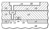
図1は、半導体装置の部分断面図を示す。半導体装置は、半導体装置基板100、フィールド絶縁領域102、および半導体装置基板100内に形成されたドープ領域104を有する。ゲート誘電体層106は半導体装置基板100の一部を被覆し、ゲート電極108はゲート誘電体層106を被覆する。
【0008】
第1合金誘電体層(ILD: interlevel dielectric layer)110は、ゲート電極108および半導体装置基板100上に形成される。第1合金誘電体層110はパターニングされ、接着/障壁層112および銅充填材料114で満たされる貫通孔(dual inlaid opening)が形成される。接着/障壁層112は一般に、耐熱金属(refractory metal)、耐熱金属窒化物、または耐熱金属若しくはそれらの窒化物の組み合わせである。銅充填材料114は一般に銅や銅合金であり、同含有率が少なくとも90原子パーセントである。銅は、マグネシウム、硫黄、炭素等とともに合金化され、接着性、エレクトロマイグレーションその他の特性を改善する。接着/障壁層112および銅充填材料114を堆積した後、基板は研磨され、接着/障壁層112および銅充填材料114の開口外側の部分が除去される。
【0009】
第1相互接続レベル(階層)が形成された後、絶縁障壁層122が銅充填接続部および第1ILD層110上に形成される。この絶縁障壁層122としては、シリコン窒化物、シリコン・オキシナイトライド(oxynitride)等を利用することが可能である。絶縁障壁層122を形成するために絶縁材料を利用すると、付加的なパターニングおよびエッチングの工程を省略することが可能になる。導電性の障壁が使用されるならば、互いに絶縁させるためにそのような付加的な工程が必要となるであろう。第2ILD層124は絶縁障壁層122上に形成される。導電性の接着/障壁層126および銅充填材料128より成る両面相互接続部(dual inlaid interconnect)が、第2ILD124内に形成される。両面相互接続部は、第1ILD層110の両面相互接続部を形成するために使用したものと同様のプロセスおよび材料を利用して形成される。
【0010】
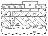
図2に示されるように、その後保護層22が第2ILD層124および両面相互接続部上に形成される。保護層は、シリコン窒化物、シリコン・オキシナイトライド、二酸化シリコン等の1以上の膜で形成することも可能である。一般に、銅充填材料128に最も近い保護層22の部分は、酸素原子よりも濃度の高い窒素原子を有するシリコン窒化物またはシリコン・オキシナイトライドとすることが可能である。保護層22はパターニングされ、その保護層を貫通して銅充填材料128に至る結合パッド開口24が形成される。
【0011】
図3に示すように、保護層22および銅充填材料128上に導電性障壁層32が堆積される。導電性障壁層32は様々なプロセスを利用して堆積させることが可能であり、そのプロセスには、化学蒸着堆積(CVD)、物理蒸着堆積(PVD)、エバポレーション堆積、電気めっき、非電気めっき(electroless plating)等が含まれる。この層の厚さは一般に50ないし300ナノメートル(nm)の範囲内にある。一般に、導電性障壁層32は耐熱金属、耐熱金属窒化物またはこれらの組み合わせを利用することが可能である。一実施例にあっては、導電性障壁層32は、チタニウム(Ti)およびチタニウム窒化物(TiN)の組み合わせより成る。チタニウム/チタニウム窒化物のスタック(積層)を利用すると、下側の銅充填材料128および保護層22との接着性を向上させることが可能である。さらに、チタニウム窒化物は、銅充填材料が以後堆積される導電性バンプと反応することを抑制する障壁層を形成する。また、導電性障壁層32としては、タンタル(Ta)、タンタル窒化物(TaN)、タングステン(W)、チタニウム・タングステン窒化物(TiWN)、チタニウム・タングステン(TiW)、タングステン窒化物(WN)、モリブデン窒化物(MoN)、コバルト窒化物(CoN)またはこれらの組み合わせを利用することが可能である。他の実施例にあっては、酸素耐性材料(oxygen tolerant material)を利用することも可能である。これらの材料には、プラチナ(Pt)、パラジウム(Pd)、ニッケル(Ni)、導電性金属酸化物またはこれらの金属に相当するものが含まれる。導電性金属酸化物およびこれらに相当する金属としては更に、イリジウム(Ir)およびイリジウム酸化物(IrO2)、ルテニウム(Ru)およびルテニウム酸化物(RuO2)、レニウム(Re)およびレニウム酸化物(ReO2およびReO3)、ならびにオスミウム(Os)およびオスミウム酸化物(OsO2)が含まれる。
【0012】
その後レジスト層34が導電性障壁層32上に形成される。レジスト層34は、保護層22を被覆する導電性障壁層32の一部を露出させている。このレジストは、結合パッド開口34を被覆するように形成される。さらに、図3に示すように、保護層22上に位置する導電性障壁層32の一部の表面上にわずかに延在するように、レジストがパターニングされる。
【0013】
その後既存のエッチング工程を利用して、導電性障壁層32はエッチングされ、保護層22上の導電性障壁層32の露出した部分が除去される。エッチング工程の後、パターニングされたレジスト層34は、プラズマ・アッシング工程またはウエット・ケミカル・エッチング工程を利用して除去され、このウエット・ケミカル・エッチング工程は、N-メチル-2-ピロリジン(N-methyl-2-pyrrolidine)、アセトン、メチル・イソブチル・ケトン(MIBK: methyl isobutyl ketone)のような有機化合物を利用するものである。
【0014】
また、電気めっきまたは非電気めっきのようなめっき工程を利用して導電性障壁層を形成する場合、上述したパターニング工程は必ずしも必要とされない。その代わりに、開口24を形成した後、導電性障壁層を銅充填材料128の露出部分上に直接めっきすることが可能である。もし必要であれば、めっきされた材料が保護層の一部分上を被覆するようにめっき処理工程を拡張し、図4に示すような導電性障壁層32を形成することも可能である。
【0015】
図5に示されるように、その後ダイ被覆層52が半導体装置上に形成されパターニングされ、結合パッド開口24上にダイ被覆開口(die coat opening)54が形成される。この実施例にあっては、導電性障壁層32の周辺部分はダイ被覆開口54内で露出した端部領域を有する。ダイ被覆層52は、感光性ポリイミド膜、または既存のレジストおよびエッチング工程を利用してパターニングされるポリイミド膜と同様にして形成することが可能である。
【0016】
図6に示されるようなパッド限定金属層62を形成するのに先立って、導電性障壁層32の露出した部分は、無線周波数(RF)スパッタ洗浄工程による処理が施される。このRFスパッタ洗浄は、導電性障壁層32の最も上側の部分を除去することにより、障壁層とパッド限定金属層との間の接触抵抗を改善するものである。除去される部分には、酸素、フッ素および塩素のような不純物が含まれている可能性がある。一実施例にあっては、RFスパッタ洗浄工程は、パッド限定金属層(バンプ下側)を堆積する前のその場所における(in situ)プロセスの一部として実行される。一実施例にあっては、RFスパッタ洗浄を行うための処理パラメータは、次のようなものである。RF電力が約1200ないし1500ワット(W)の範囲内にあり、直流(DC)バイアス電圧が約(−300)ないし(−600)ボルト(V)であり、圧力が約0.1ないし0.5パスカルの範囲内にあり、時間は約150ないし250秒の範囲内にある。RFスパッタ洗浄工程は、障壁層32の表面から約20−40nmの障壁材料を除去する。
【0017】
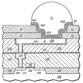
図6に示されるように、その後パッド限定金属層62がダイ被覆開口54内に形成される。パッド限定金属層は一般に、薄膜の機能的な組み合わせとすることが可能であり、その薄膜には、接着層、中間結合/半田層および非酸化障壁層等がある。一実施例にあっては、パッド限定金属層62は4つの個別薄膜より成る。すなわち、クロム層622、クロム−銅合金層624、銅層626および金層628である。クロム層622およびクロム−銅合金層624は夫々50ないし500nmの範囲内の厚さを有し、銅層626は約700ないし1300nmの範囲内の厚さを有し、金層628は80ないし140nmの範囲内の厚さを有する。また、パッド限定金属層は、チタニウム、銅および金の複合物またはチタニウム、ニッケル、銅および金の複合物のような他の薄膜の組み合わせとすることも可能である。パッド限定金属層62は一般に、浅いマスクを利用してエバポレーションにより形成される。しかしながら、スパッタリングのような他の手法を利用してパッド限定金属層を形成することも可能である。
【0018】
図7に示されるように一実施例によれば、パッド限定金属層を形成した後に、鉛スズ半田材料72のようなバンプ材料がパッド限定金属層62上に堆積される。鉛スズ半田材料72は浅いマスクを利用してエバポレーションにより形成することが可能であり、また、めっき又は半田ジェット(solderjetting)のような既存の他の手法を利用して形成することも可能である。その後リフロー工程が行われ、鉛スズ半田材料72の角を丸め、図7に示されるようなバンプが形成される。
【0019】
この時点において、実質的には半導体装置は完成している。その後この装置は、フリップ・チップまたはボール・グリッド・アレイ・パッケージのようなパッケージ基板に接着される。図示されてはいないが、必要に応じて相互接続部の他のレベル(階層)を形成することも可能である。他の相互接続部も同様に、ゲート電極108およびドープ領域104に対して形成することが可能である。このような付加的な相互接続部を形成するには、絶縁層122、第2ILD層124、接着/障壁層126および銅充填材料128を形成および堆積するのに使用したものと同様のプロセスを利用することが可能であろう。
【0020】
図8ないし12は、本発明の他の実施例に関するものである。図8では、導電性障壁層82が第2ILD層124および銅充填材料128上に形成されている。導電性障壁層82は、図3の第1実施例の導電性障壁層32を形成する際に説明した方法および材料を利用して形成される。導電性障壁層82の厚さは一般に50ないし300nmの範囲内にある。この実施例にあっては、選択的な耐酸化層(oxidation-resistant)84が導電性障壁層82上に形成されている。耐酸化層としては、下側の層の酸化を防止する又は下側の層に優先して容易に酸化されやすい任意の材料を利用することが可能である。使用可能な材料としては、シリコン窒化物、ポリシリコン、アモルファス・シリコンまたは導電性金属酸化物若しくはその金属等がある。耐酸化層84は約10−50nmの範囲内の厚さを有する。その後、この導電性障壁層82および耐酸化層84上にレジスト層86が形成される。レジスト層86はパターニングされ、導電性障壁層82の一部と、銅充填材料128および接着/障壁層126上の耐酸化層84とが被覆される。
【0021】
導電性障壁層82および耐酸化層84のパターニングされていない部分は、既存のエッチング工程を利用して除去される。その後レジストは除去され、図9に示されるように、導電性障壁層82、耐酸化層84および誘電体層124の一部より成る積層(スタック)上に保護層92形成される。保護層92は、図2の第1実施例の保護層22と同様のものである。この実施例にあっては、保護層92はパターニングされ、結合パッド開口94が形成される。図9に図示されているように、結合パッド開口94内の保護層の総てが除去されるわけではない。したがって、結合パッド開口は、パターニング工程において部分的に形成されるに過ぎない。残余の部分96は、パターニングが完了した後も耐酸化層84上にとり残される。
【0022】
図10に示されるように、ダイ被覆開口1003を形成およびパターニングするためにダイ被覆層1001が形成される。このダイ被覆層1001は図5の第1実施例のダイ被覆層52と同様のものである。ダイ被覆開口1003は、残余部分96を含む保護層92の一部を露出させる。ダイ被覆開口1003を形成した後、エッチングが行われ、残余部分96および下側の耐酸化層84が除去される。このようにして、図11に示されるようなダイ被覆開口1003が形成される。このエッチングにおいて、ダイ被覆層1001により露出させられた保護層92の部分もエッチングされ、これは除去された保護層部分1102として図示されている。一実施例にあっては、保護層92はシリコン窒化物またはシリコン・オキシナイトライドのようなシリコンおよび窒素を含み、耐酸化層84はシリコン窒化物を含む。このため、同一のまたは同様のエッチング環境を利用して、保護層92の残余部分96および耐酸化層84を除去することが可能である。
【0023】
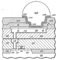
その後プロセスが進行すると、図12に示されるように装置が実質的に完成する。パッド限定金属層1220が、先に説明したものと同様に形成され、この層は、クロム層1222、クロム−銅層1224、銅層1226、金層1228および鉛スズ半田1230を含む。上述したものと同様に、必要に応じてRFスパッタ洗浄工程を利用して、パッド限定金属層1220を形成するのに先立って障壁層の表面に処理を施すことも可能である。この実施例にあっては、リフロー工程を実行し、鉛スズ半田の形状を丸くし、図12に示されるようなドーム状の形を形成する。
【0024】
図9ないし12に関連する実施例にあっては、最上部の相互接続レベルを除く総ての相互接続レベルに対して、絶縁障壁層122が使用される。最上部の相互接続レベルは、結合パッドが形成される部分上の相互接続レベルである。したがって、最上部の相互接続レベルは、導電性障壁層82を利用する唯一の相互接続レベルである。
【0025】
本発明に関連して多数の実施例が存在し得る。図3に戻って、導電性障壁層32は、図8−12の第2実施例の耐酸化層84と同様な耐酸化被覆層を利用することも可能である。同様に、第2実施例は耐酸化層84を必ずしも必要としない。なぜなら、保護層92の残余部分96は、導電性障壁層82に損傷を与えることなく酸素含有プラズマを利用することを許容するからである。このことは次のような場合に特に重要である。すなわち導電性障壁層82または32が、酸素含有プラズマまたはレジストやポリイミドを除去・現像するための他の化学物質に対して適切に反応することが可能なタンタル窒化物、チタニウム窒化物等を含む場合である。このような化学物質の例としては、テトラメチル・アンモニウム水酸化物(tetramethyl ammonium hydroxide)、N-メトキシ-2-ピロリジン、アセトンMIBK等がある。
【0026】
図9−12で説明したような結合パッド上に導電性障壁層を形成することに加えて、導電性障壁材料を利用して、半導体装置の導電性領域間にレーザ可変接続部または集束エネルギ可変(focused energy-alterable)接続部を形成することも可能である。プログラム又は装置の回路に適合させるために、その接続部の導電率はレーザを利用して修正されることが可能である。
【0027】
導電性障壁層を利用するレーザ可変接続部を形成すると、既存の技術に比較して有利な点がある。レーザ可変接続部を形成するために通常使用される導電性障壁層は一般に、相互接続層よりも、非常に薄く、熱伝導性が低く、耐熱性が低い。導電性障壁層は、相互接続層に比較して自ら保護するもの(self-passivating)もある。したがって、レーザ可変が実行された後の短絡に対する電位は減少させられるので、レーザ可変の信頼性は大幅に向上する。さらに、レーザ可変接続部は、半導体装置の最上部表面に近接して形成される。このため、レーザ可変接続部を修正するために使用するレーザの電力は少なくてすみ、それに応じて短絡、接続部近傍への損傷および包囲する保護層の損傷も少なくなる。さらに、導電性障壁層およびレーザ可変接続部は、同一の層を利用して同時に形成されることも可能である。従ってこの場合は、製造工程数を増加させる必要はなくなる。
【0028】
パッド限定金属層62に対していくつかの材料が列挙されたが、必要に応じてたの材料を利用することも可能であろう。例えば、導電性障壁層は、パッド限定金属層の一部として組み込むことも可能である。この場合は、他のパッド限定金属層が形成される前に、ウエファ上にそれをエバポレーション又はスパッタリングにより形成することも可能である。更なる実施例にあっては、パッド限定金属層およびはんだ材料は、物理的蒸着堆積(PVD)により又は噴霧塗布(jet printing)により集約的に形成され、溶融した半田のしたたりが、オリフィス近辺の場所に堆積される。
【0029】
以上説明した実施例は、新種の材料、新プロセスの開発または新装置の購入を必要とすることなく、既存の処理工程に組み込まれることが可能である。導電性障壁層32および82は、相互接続部からの銅およびバンプからの鉛スズ半田が、互いに反応してしまうことを充分に防止する。このため、バンプおよび相互接続部間のインターフェースにおける完全性ないし信頼性が向上する。このことは、バンプの機械的信頼性だけでなく、バンプおよび相互接続部間の電気抵抗を減少させることにも寄与する。
【0030】
以上本発明をいくつかの実施例とともに説明してきた。しかしながら、実施例および図面は、本発明を限定的に解釈させようとするものではない。当業者であれば、本発明の精神から逸脱することなく、様々な修正や改良等をすることが可能であろう。
【図面の簡単な説明】
【図1】本発明の第1実施例による銅の接続部およびバンプを有する半導体装置を形成する工程における部分断面図を示す。
【図2】本発明の第1実施例による銅の接続部およびバンプを有する半導体装置を形成する工程における部分断面図を示す。
【図3】本発明の第1実施例による銅の接続部およびバンプを有する半導体装置を形成する工程における部分断面図を示す。
【図4】本発明の第1実施例による銅の接続部およびバンプを有する半導体装置を形成する工程における部分断面図を示す。
【図5】本発明の第1実施例による銅の接続部およびバンプを有する半導体装置を形成する工程における部分断面図を示す。
【図6】本発明の第1実施例による銅の接続部およびバンプを有する半導体装置を形成する工程における部分断面図を示す。
【図7】本発明の第1実施例による銅の接続部およびバンプを有する半導体装置を形成する工程における部分断面図を示す。
【図8】本発明の第2実施例による銅の接続部およびバンプを有する半導体装置を形成する工程における部分断面図を示す。
【図9】本発明の第2実施例による銅の接続部およびバンプを有する半導体装置を形成する工程における部分断面図を示す。
【図10】本発明の第2実施例による銅の接続部およびバンプを有する半導体装置を形成する工程における部分断面図を示す。
【図11】本発明の第2実施例による銅の接続部およびバンプを有する半導体装置を形成する工程における部分断面図を示す。
【図12】本発明の第2実施例による銅の接続部およびバンプを有する半導体装置を形成する工程における部分断面図を示す。
【符号の説明】
22 保護層
24 開口
32 導電性障壁層
34 レジスト
52 ダイ・コート層
54 開口
62 パッド限定金属層
72 鉛スズ半田材料
82 導電性障壁層
84 耐酸化層
86 レジスト
92 保護層
94 開口
96 保護層の残余部分
100 半導体装置基板
102 フィールド絶縁層
104 ドープ領域
106 ゲート誘電体
108 ゲート電極
110 第1合金誘電体(ILD)層
112 接着/障壁層
114 相互接続部
122 絶縁障壁層
124 第2合金誘電体(ILD)層
126 接着/障壁層
128 銅含有相互接続部
1001 ダイ被覆層
1003 開口
1220 パッド限定金属層
1230 導電性バンプ
Claims (5)
- 半導体装置を製造する方法であって、
半導体装置基板(100)上に第1相互接続部(114)を形成する段階と、
前記第1相互接続部(114)の一部を覆うように第2相互接続部(128)を形成する段階であって、第2相互接続部(128)は、結合パッド部を含む銅相互接続部としての特徴を有している段階と、
前記結合パッド部上に導電性障壁層(82)を形成する段階と、
前記導電性障壁層上に耐酸化層(84)を形成する段階と、
前記耐酸化層上に保護層(92)を形成する段階と、
前記保護層(92)に開口(94)の一部を形成する段階であって、前記開口の一部の深さは、同開口の一部が形成される保護層の領域において同保護層の厚さより小さい段階と、
前記保護層(92)上にダイ被覆層(1001)を形成する段階と、
前記ダイ被覆層(1001)に開口(1003)を形成する段階であって、前記ダイ被覆層に開口(1003)を形成する段階は、前記保護層(92)の開口(94)の一部を露出させ、かつ前記保護層において前記保護層(92)の開口(94)の一部のエッジ領域周辺の保護層を除去する段階を含む段階と、
前記ダイ被覆層(1001)に開口(1003)を形成した後、前記導電性障壁層(82)を露出させるため、前記保護層(92)の開口(94)を介してエッチングを行う段階と、
前記導電性障壁層(82)上にパッド限定金属層(1220)を形成する段階であって、前記パッド限定金属層(1220)はクロム層を含み、前記クロム層は前記導電性障壁層(82)と接触する段階と、
前記パッド限定金属層(1220)上に導電性バンプ(1230)を形成する段階と
を備える方法。 - 前記導電性障壁層(82)の一部は、少なくとも2つの導電性領域の間に位置するレーザ可変接続部である請求項1記載の方法。
- 前記耐酸化層(84)は、シリコン窒化物を含むか、或いは、前記耐酸化層は、シリコン層である請求項1記載の方法。
- 前記導電性障壁層(82)は、チタニウム、タンタル、及びタングステンからなる群より選ばれた材料を含むか、或いは、タンタル窒化物、チタニウムタングステン窒化物、チタニウムタングステン、タングステン窒化物、モリブデン窒化物及びコバルト窒化物のうち少なくとも一つを含むか、或いは、プラチナ、パラジウム及びニッケルのうち少なくとも一つを含むか、或いは、イリジウム、イリジウム酸化物、ルテニウム、ルテニウム酸化物、レニウム、レニウム酸化物、オスミウム及びオスミウム酸化物のうち少なくとも一つを含む請求項1記載の方法。
- 前記導電性障壁層(82)は、耐熱金属及び耐熱金属窒化物の組合せを含むか、或いは、チタニウム及びチタニウム窒化物を含む請求項1記載の方法。
Applications Claiming Priority (2)
| Application Number | Priority Date | Filing Date | Title |
|---|---|---|---|
| US285666 | 1981-07-21 | ||
| US09/285,666 US20020000665A1 (en) | 1999-04-05 | 1999-04-05 | Semiconductor device conductive bump and interconnect barrier |
Publications (3)
| Publication Number | Publication Date |
|---|---|
| JP2000306914A JP2000306914A (ja) | 2000-11-02 |
| JP2000306914A5 JP2000306914A5 (ja) | 2007-05-17 |
| JP4566325B2 true JP4566325B2 (ja) | 2010-10-20 |
Family
ID=23095213
Family Applications (1)
| Application Number | Title | Priority Date | Filing Date |
|---|---|---|---|
| JP2000086214A Expired - Fee Related JP4566325B2 (ja) | 1999-04-05 | 2000-03-27 | 半導体装置を製造する方法 |
Country Status (5)
| Country | Link |
|---|---|
| US (2) | US20020000665A1 (ja) |
| JP (1) | JP4566325B2 (ja) |
| CN (1) | CN1192430C (ja) |
| SG (1) | SG84587A1 (ja) |
| TW (1) | TW490793B (ja) |
Families Citing this family (115)
| Publication number | Priority date | Publication date | Assignee | Title |
|---|---|---|---|---|
| US6577011B1 (en) * | 1997-07-10 | 2003-06-10 | International Business Machines Corporation | Chip interconnect wiring structure with low dielectric constant insulator and methods for fabricating the same |
| JPH11340265A (ja) * | 1998-05-22 | 1999-12-10 | Sony Corp | 半導体装置及びその製造方法 |
| DE19843624C1 (de) * | 1998-09-23 | 2000-06-15 | Siemens Ag | Integrierte Schaltungsanordnung und Verfahren zu deren Herstellung |
| US6303423B1 (en) * | 1998-12-21 | 2001-10-16 | Megic Corporation | Method for forming high performance system-on-chip using post passivation process |
| US6965165B2 (en) * | 1998-12-21 | 2005-11-15 | Mou-Shiung Lin | Top layers of metal for high performance IC's |
| US8178435B2 (en) * | 1998-12-21 | 2012-05-15 | Megica Corporation | High performance system-on-chip inductor using post passivation process |
| US7531417B2 (en) * | 1998-12-21 | 2009-05-12 | Megica Corporation | High performance system-on-chip passive device using post passivation process |
| US7405149B1 (en) | 1998-12-21 | 2008-07-29 | Megica Corporation | Post passivation method for semiconductor chip or wafer |
| US7381642B2 (en) * | 2004-09-23 | 2008-06-03 | Megica Corporation | Top layers of metal for integrated circuits |
| US6544880B1 (en) * | 1999-06-14 | 2003-04-08 | Micron Technology, Inc. | Method of improving copper interconnects of semiconductor devices for bonding |
| US6077766A (en) * | 1999-06-25 | 2000-06-20 | International Business Machines Corporation | Variable thickness pads on a substrate surface |
| JP4554011B2 (ja) * | 1999-08-10 | 2010-09-29 | ルネサスエレクトロニクス株式会社 | 半導体集積回路装置の製造方法 |
| US6570251B1 (en) * | 1999-09-02 | 2003-05-27 | Micron Technology, Inc. | Under bump metalization pad and solder bump connections |
| JP3859403B2 (ja) * | 1999-09-22 | 2006-12-20 | 株式会社東芝 | 半導体装置及びその製造方法 |
| US7494927B2 (en) | 2000-05-15 | 2009-02-24 | Asm International N.V. | Method of growing electrical conductors |
| JP3824845B2 (ja) * | 2000-06-21 | 2006-09-20 | セイコーエプソン株式会社 | Lcdドライバicチップ |
| DE60108413T2 (de) * | 2000-11-10 | 2005-06-02 | Unitive Electronics, Inc. | Verfahren zum positionieren von komponenten mit hilfe flüssiger antriebsmittel und strukturen hierfür |
| US6753605B2 (en) * | 2000-12-04 | 2004-06-22 | Fairchild Semiconductor Corporation | Passivation scheme for bumped wafers |
| WO2002052646A1 (en) * | 2000-12-22 | 2002-07-04 | Koninklijke Philips Electronics N.V. | Integrated circuit device |
| US6794705B2 (en) * | 2000-12-28 | 2004-09-21 | Infineon Technologies Ag | Multi-layer Pt electrode for DRAM and FRAM with high K dielectric materials |
| JP2003045877A (ja) * | 2001-08-01 | 2003-02-14 | Sharp Corp | 半導体装置およびその製造方法 |
| US6759275B1 (en) | 2001-09-04 | 2004-07-06 | Megic Corporation | Method for making high-performance RF integrated circuits |
| US7049226B2 (en) * | 2001-09-26 | 2006-05-23 | Applied Materials, Inc. | Integration of ALD tantalum nitride for copper metallization |
| US6762122B2 (en) * | 2001-09-27 | 2004-07-13 | Unitivie International Limited | Methods of forming metallurgy structures for wire and solder bonding |
| US6916398B2 (en) * | 2001-10-26 | 2005-07-12 | Applied Materials, Inc. | Gas delivery apparatus and method for atomic layer deposition |
| JP3820975B2 (ja) * | 2001-12-12 | 2006-09-13 | ソニー株式会社 | 半導体装置及びその製造方法 |
| US6661098B2 (en) * | 2002-01-18 | 2003-12-09 | International Business Machines Corporation | High density area array solder microjoining interconnect structure and fabrication method |
| JP4340416B2 (ja) * | 2002-02-26 | 2009-10-07 | Spansion Japan株式会社 | 半導体記憶装置の製造方法 |
| WO2004001837A2 (en) * | 2002-06-25 | 2003-12-31 | Unitive International Limited | Methods of forming electronic structures including conductive shunt layers and related structures |
| US7531898B2 (en) * | 2002-06-25 | 2009-05-12 | Unitive International Limited | Non-Circular via holes for bumping pads and related structures |
| US7547623B2 (en) * | 2002-06-25 | 2009-06-16 | Unitive International Limited | Methods of forming lead free solder bumps |
| JP3779243B2 (ja) | 2002-07-31 | 2006-05-24 | 富士通株式会社 | 半導体装置及びその製造方法 |
| JP2004214594A (ja) * | 2002-11-15 | 2004-07-29 | Sharp Corp | 半導体装置およびその製造方法 |
| DE10301243B4 (de) * | 2003-01-15 | 2009-04-16 | Infineon Technologies Ag | Verfahren zum Herstellen einer integrierten Schaltungsanordnung, insbesondere mit Kondensatoranordnung |
| JP4170103B2 (ja) * | 2003-01-30 | 2008-10-22 | Necエレクトロニクス株式会社 | 半導体装置、および半導体装置の製造方法 |
| US6869878B1 (en) * | 2003-02-14 | 2005-03-22 | Advanced Micro Devices, Inc. | Method of forming a selective barrier layer using a sacrificial layer |
| TWI225899B (en) * | 2003-02-18 | 2005-01-01 | Unitive Semiconductor Taiwan C | Etching solution and method for manufacturing conductive bump using the etching solution to selectively remove barrier layer |
| US7026714B2 (en) * | 2003-03-18 | 2006-04-11 | Cunningham James A | Copper interconnect systems which use conductive, metal-based cap layers |
| JP4571781B2 (ja) * | 2003-03-26 | 2010-10-27 | ルネサスエレクトロニクス株式会社 | 半導体装置およびその製造方法 |
| US7238610B2 (en) * | 2003-03-31 | 2007-07-03 | Intel Corporation | Method and apparatus for selective deposition |
| US7566964B2 (en) * | 2003-04-10 | 2009-07-28 | Agere Systems Inc. | Aluminum pad power bus and signal routing for integrated circuit devices utilizing copper technology interconnect structures |
| US6893959B2 (en) * | 2003-05-05 | 2005-05-17 | Infineon Technologies Ag | Method to form selective cap layers on metal features with narrow spaces |
| DE10335182B4 (de) * | 2003-07-30 | 2007-03-01 | Infineon Technologies Ag | Anordnung zur Verbesserung der Modulzuverlässigkeit |
| DE10337569B4 (de) * | 2003-08-14 | 2008-12-11 | Infineon Technologies Ag | Integrierte Anschlussanordnung und Herstellungsverfahren |
| US6977435B2 (en) * | 2003-09-09 | 2005-12-20 | Intel Corporation | Thick metal layer integrated process flow to improve power delivery and mechanical buffering |
| WO2005024912A2 (en) * | 2003-09-09 | 2005-03-17 | Intel Corporation | Methods of processing thick ild layers using spray coating or lamination for c4 wafer level thick metal integrated flow |
| IL157838A (en) * | 2003-09-10 | 2013-05-30 | Yaakov Amitai | High-brightness optical device |
| US7294565B2 (en) * | 2003-10-01 | 2007-11-13 | International Business Machines Corporation | Method of fabricating a wire bond pad with Ni/Au metallization |
| US6933171B2 (en) * | 2003-10-21 | 2005-08-23 | Intel Corporation | Large bumps for optical flip chips |
| US7451975B2 (en) * | 2004-03-18 | 2008-11-18 | Lexmark International, Inc. | Input tray and drive mechanism using a single motor for an image forming device |
| JP2005347622A (ja) * | 2004-06-04 | 2005-12-15 | Seiko Epson Corp | 半導体装置、回路基板及び電子機器 |
| US8552559B2 (en) * | 2004-07-29 | 2013-10-08 | Megica Corporation | Very thick metal interconnection scheme in IC chips |
| US7355282B2 (en) | 2004-09-09 | 2008-04-08 | Megica Corporation | Post passivation interconnection process and structures |
| US8008775B2 (en) | 2004-09-09 | 2011-08-30 | Megica Corporation | Post passivation interconnection structures |
| DE102004048202B4 (de) * | 2004-09-30 | 2008-05-21 | Infineon Technologies Ag | Verfahren zur Vereinzelung von oberflächenmontierbaren Halbleiterbauteilen und zur Bestückung derselben mit Außenkontakten |
| US20060205170A1 (en) * | 2005-03-09 | 2006-09-14 | Rinne Glenn A | Methods of forming self-healing metal-insulator-metal (MIM) structures and related devices |
| US20060205204A1 (en) * | 2005-03-14 | 2006-09-14 | Michael Beck | Method of making a semiconductor interconnect with a metal cap |
| US7666773B2 (en) | 2005-03-15 | 2010-02-23 | Asm International N.V. | Selective deposition of noble metal thin films |
| US8025922B2 (en) | 2005-03-15 | 2011-09-27 | Asm International N.V. | Enhanced deposition of noble metals |
| US8384189B2 (en) * | 2005-03-29 | 2013-02-26 | Megica Corporation | High performance system-on-chip using post passivation process |
| JP2007005539A (ja) * | 2005-06-23 | 2007-01-11 | Seiko Epson Corp | 半導体装置 |
| JP4605378B2 (ja) | 2005-07-13 | 2011-01-05 | セイコーエプソン株式会社 | 半導体装置 |
| US20070014919A1 (en) * | 2005-07-15 | 2007-01-18 | Jani Hamalainen | Atomic layer deposition of noble metal oxides |
| CN1901163B (zh) * | 2005-07-22 | 2011-04-13 | 米辑电子股份有限公司 | 连续电镀制作线路组件的方法及线路组件结构 |
| US7960838B2 (en) | 2005-11-18 | 2011-06-14 | United Microelectronics Corp. | Interconnect structure |
| US7932615B2 (en) * | 2006-02-08 | 2011-04-26 | Amkor Technology, Inc. | Electronic devices including solder bumps on compliant dielectric layers |
| KR100735526B1 (ko) * | 2006-02-08 | 2007-07-04 | 삼성전자주식회사 | 와이어 본딩 신뢰성이 향상된 반도체 소자, 이의 제조에사용되는 레티클, 및 그 제조 방법 |
| US7674701B2 (en) | 2006-02-08 | 2010-03-09 | Amkor Technology, Inc. | Methods of forming metal layers using multi-layer lift-off patterns |
| US8421227B2 (en) * | 2006-06-28 | 2013-04-16 | Megica Corporation | Semiconductor chip structure |
| US8592977B2 (en) * | 2006-06-28 | 2013-11-26 | Megit Acquisition Corp. | Integrated circuit (IC) chip and method for fabricating the same |
| TWI460820B (zh) * | 2006-06-28 | 2014-11-11 | Qualcomm Inc | 積體電路(ic)晶片及其製程 |
| US20080038913A1 (en) * | 2006-08-10 | 2008-02-14 | International Business Machines Corporation | Methods of forming aluminum-free wire bond pad and pad so formed |
| US7435484B2 (en) * | 2006-09-01 | 2008-10-14 | Asm Japan K.K. | Ruthenium thin film-formed structure |
| DE102006051490B4 (de) * | 2006-10-31 | 2010-07-08 | Advanced Micro Devices, Inc., Sunnyvale | Technik zur Herstellung einer Passivierungsschicht ohne ein Abschlussmetall |
| DE102006051491A1 (de) * | 2006-10-31 | 2008-05-15 | Advanced Micro Devices, Inc., Sunnyvale | Metallisierungsschichtstapel mit einer Aluminiumabschlussmetallschicht |
| WO2008054680A2 (en) * | 2006-10-31 | 2008-05-08 | Advanced Micro Devices, Inc. | A metallization layer stack without a terminal aluminum metal layer |
| US8193636B2 (en) * | 2007-03-13 | 2012-06-05 | Megica Corporation | Chip assembly with interconnection by metal bump |
| US7682959B2 (en) * | 2007-03-21 | 2010-03-23 | Stats Chippac, Ltd. | Method of forming solder bump on high topography plated Cu |
| US8030733B1 (en) | 2007-05-22 | 2011-10-04 | National Semiconductor Corporation | Copper-compatible fuse target |
| US7964934B1 (en) | 2007-05-22 | 2011-06-21 | National Semiconductor Corporation | Fuse target and method of forming the fuse target in a copper process flow |
| DE102007046519A1 (de) * | 2007-09-28 | 2009-04-02 | Osram Opto Semiconductors Gmbh | Dünnfilm-LED mit einer Spiegelschicht und Verfahren zu deren Herstellung |
| US20090087339A1 (en) * | 2007-09-28 | 2009-04-02 | Asm Japan K.K. | METHOD FOR FORMING RUTHENIUM COMPLEX FILM USING Beta-DIKETONE-COORDINATED RUTHENIUM PRECURSOR |
| KR101544198B1 (ko) * | 2007-10-17 | 2015-08-12 | 한국에이에스엠지니텍 주식회사 | 루테늄 막 형성 방법 |
| US7829450B2 (en) * | 2007-11-07 | 2010-11-09 | Infineon Technologies Ag | Method of processing a contact pad, method of manufacturing a contact pad, and integrated circuit element |
| DE102007057689A1 (de) * | 2007-11-30 | 2009-06-04 | Advanced Micro Devices, Inc., Sunnyvale | Halbleiterbauelement mit einem Chipgebiet, das für eine aluminiumfreie Lothöckerverbindung gestaltet ist, und eine Teststruktur, die für eine aluminiumfreie Drahtverbindung gestaltet ist |
| KR20090067505A (ko) * | 2007-12-21 | 2009-06-25 | 에이에스엠지니텍코리아 주식회사 | 루테늄막 증착 방법 |
| CN101630667A (zh) | 2008-07-15 | 2010-01-20 | 中芯国际集成电路制造(上海)有限公司 | 形成具有铜互连的导电凸块的方法和系统 |
| US8084104B2 (en) * | 2008-08-29 | 2011-12-27 | Asm Japan K.K. | Atomic composition controlled ruthenium alloy film formed by plasma-enhanced atomic layer deposition |
| US7709956B2 (en) * | 2008-09-15 | 2010-05-04 | National Semiconductor Corporation | Copper-topped interconnect structure that has thin and thick copper traces and method of forming the copper-topped interconnect structure |
| US8133555B2 (en) | 2008-10-14 | 2012-03-13 | Asm Japan K.K. | Method for forming metal film by ALD using beta-diketone metal complex |
| US9379011B2 (en) | 2008-12-19 | 2016-06-28 | Asm International N.V. | Methods for depositing nickel films and for making nickel silicide and nickel germanide |
| US20100155949A1 (en) * | 2008-12-24 | 2010-06-24 | Texas Instruments Incorporated | Low cost process flow for fabrication of metal capping layer over copper interconnects |
| US20110020546A1 (en) * | 2009-05-15 | 2011-01-27 | Asm International N.V. | Low Temperature ALD of Noble Metals |
| US8329569B2 (en) * | 2009-07-31 | 2012-12-11 | Asm America, Inc. | Deposition of ruthenium or ruthenium dioxide |
| US8003515B2 (en) * | 2009-09-18 | 2011-08-23 | Infineon Technologies Ag | Device and manufacturing method |
| KR101652386B1 (ko) * | 2009-10-01 | 2016-09-12 | 삼성전자주식회사 | 집적회로 칩 및 이의 제조방법과 집적회로 칩을 구비하는 플립 칩 패키지 및 이의 제조방법 |
| KR20110106751A (ko) * | 2010-03-23 | 2011-09-29 | 삼성전자주식회사 | 반도체 소자 및 전자 시스템 |
| JP5342532B2 (ja) | 2010-10-05 | 2013-11-13 | 三菱重工業株式会社 | 車体フレームの製造方法 |
| US8492892B2 (en) * | 2010-12-08 | 2013-07-23 | International Business Machines Corporation | Solder bump connections |
| DE102011005642B4 (de) | 2011-03-16 | 2012-09-27 | GLOBALFOUNDRIES Dresden Module One Ltd. Liability Company & Co. KG | Verfahren zum Schutz von reaktiven Metalloberflächen von Halbleiterbauelementen während des Transports durch Bereitstellen einer zusätzlichen Schutzschicht |
| US8871617B2 (en) | 2011-04-22 | 2014-10-28 | Asm Ip Holding B.V. | Deposition and reduction of mixed metal oxide thin films |
| US8716858B2 (en) * | 2011-06-24 | 2014-05-06 | Taiwan Semiconductor Manufacturing Company, Ltd. | Bump structure with barrier layer on post-passivation interconnect |
| US8946000B2 (en) | 2013-02-22 | 2015-02-03 | Freescale Semiconductor, Inc. | Method for forming an integrated circuit having a programmable fuse |
| KR102387275B1 (ko) * | 2015-02-25 | 2022-04-15 | 인텔 코포레이션 | 마이크로전자 구조체 내의 상호연결 패드를 위한 표면 마감부 |
| US9607842B1 (en) | 2015-10-02 | 2017-03-28 | Asm Ip Holding B.V. | Methods of forming metal silicides |
| US9704804B1 (en) * | 2015-12-18 | 2017-07-11 | Texas Instruments Incorporated | Oxidation resistant barrier metal process for semiconductor devices |
| CN107871669B (zh) * | 2016-09-28 | 2021-02-05 | 欣兴电子股份有限公司 | 组装方法 |
| US10204859B2 (en) * | 2017-01-25 | 2019-02-12 | Macronix International Co., Ltd. | Interconnect structure and fabricating method thereof |
| US10629334B2 (en) * | 2017-09-20 | 2020-04-21 | Texas Instruments Incorporated | Nanostructure barrier for copper wire bonding |
| US10658315B2 (en) * | 2018-03-27 | 2020-05-19 | Taiwan Semiconductor Manufacturing Co., Ltd. | Redistribution layer metallic structure and method |
| US11367683B2 (en) | 2018-07-03 | 2022-06-21 | Infineon Technologies Ag | Silicon carbide device and method for forming a silicon carbide device |
| US11869840B2 (en) | 2018-07-03 | 2024-01-09 | Infineon Technologies Ag | Silicon carbide device and method for forming a silicon carbide device |
| US11189538B2 (en) * | 2018-09-28 | 2021-11-30 | Taiwan Semiconductor Manufacturing Co., Ltd. | Semiconductor structure with polyimide packaging and manufacturing method |
| US11948848B2 (en) * | 2019-02-12 | 2024-04-02 | Intel Corporation | Subtractive etch resolution implementing a functional thin metal resist |
| US11244914B2 (en) | 2020-05-05 | 2022-02-08 | Taiwan Semiconductor Manufacturing Company, Ltd. | Bond pad with enhanced reliability |
Citations (3)
| Publication number | Priority date | Publication date | Assignee | Title |
|---|---|---|---|---|
| JPS63293951A (ja) * | 1987-05-27 | 1988-11-30 | Hitachi Ltd | 半導体素子電極構造 |
| JPH05114655A (ja) * | 1991-06-27 | 1993-05-07 | Hitachi Ltd | 半導体集積回路装置およびその製造方法 |
| JPH11340265A (ja) * | 1998-05-22 | 1999-12-10 | Sony Corp | 半導体装置及びその製造方法 |
Family Cites Families (10)
| Publication number | Priority date | Publication date | Assignee | Title |
|---|---|---|---|---|
| US5220199A (en) * | 1988-09-13 | 1993-06-15 | Hitachi, Ltd. | Semiconductor integrated circuit device in which a semiconductor chip is mounted with solder bumps for mounting to a wiring substrate |
| US5470787A (en) * | 1994-05-02 | 1995-11-28 | Motorola, Inc. | Semiconductor device solder bump having intrinsic potential for forming an extended eutectic region and method for making and using the same |
| US5656858A (en) | 1994-10-19 | 1997-08-12 | Nippondenso Co., Ltd. | Semiconductor device with bump structure |
| JP2985692B2 (ja) * | 1994-11-16 | 1999-12-06 | 日本電気株式会社 | 半導体装置の配線構造及びその製造方法 |
| JPH08191104A (ja) * | 1995-01-11 | 1996-07-23 | Hitachi Ltd | 半導体集積回路装置およびその製造方法 |
| EP0815593B1 (en) * | 1995-03-20 | 2001-12-12 | Unitive International Limited | Solder bump fabrication methods and structure including a titanium barrier layer |
| US5731624A (en) | 1996-06-28 | 1998-03-24 | International Business Machines Corporation | Integrated pad and fuse structure for planar copper metallurgy |
| JP3660799B2 (ja) * | 1997-09-08 | 2005-06-15 | 株式会社ルネサステクノロジ | 半導体集積回路装置の製造方法 |
| JP3697044B2 (ja) * | 1997-12-19 | 2005-09-21 | 株式会社ルネサステクノロジ | 半導体集積回路装置およびその製造方法 |
| US6187680B1 (en) | 1998-10-07 | 2001-02-13 | International Business Machines Corporation | Method/structure for creating aluminum wirebound pad on copper BEOL |
-
1999
- 1999-04-05 US US09/285,666 patent/US20020000665A1/en not_active Abandoned
-
2000
- 2000-03-27 JP JP2000086214A patent/JP4566325B2/ja not_active Expired - Fee Related
- 2000-04-01 TW TW089106143A patent/TW490793B/zh not_active IP Right Cessation
- 2000-04-04 SG SG200001904A patent/SG84587A1/en unknown
- 2000-04-04 CN CNB001049275A patent/CN1192430C/zh not_active Expired - Fee Related
-
2002
- 2002-01-18 US US10/051,262 patent/US6713381B2/en not_active Expired - Fee Related
Patent Citations (3)
| Publication number | Priority date | Publication date | Assignee | Title |
|---|---|---|---|---|
| JPS63293951A (ja) * | 1987-05-27 | 1988-11-30 | Hitachi Ltd | 半導体素子電極構造 |
| JPH05114655A (ja) * | 1991-06-27 | 1993-05-07 | Hitachi Ltd | 半導体集積回路装置およびその製造方法 |
| JPH11340265A (ja) * | 1998-05-22 | 1999-12-10 | Sony Corp | 半導体装置及びその製造方法 |
Also Published As
| Publication number | Publication date |
|---|---|
| US20020000665A1 (en) | 2002-01-03 |
| CN1269607A (zh) | 2000-10-11 |
| TW490793B (en) | 2002-06-11 |
| US6713381B2 (en) | 2004-03-30 |
| SG84587A1 (en) | 2001-11-20 |
| CN1192430C (zh) | 2005-03-09 |
| JP2000306914A (ja) | 2000-11-02 |
| US20020093098A1 (en) | 2002-07-18 |
Similar Documents
| Publication | Publication Date | Title |
|---|---|---|
| JP4566325B2 (ja) | 半導体装置を製造する方法 | |
| TW522538B (en) | Semiconductor device and method of manufacturing the semiconductor device | |
| USRE46147E1 (en) | Semiconductor device and method of fabricating the same | |
| US8319343B2 (en) | Routing under bond pad for the replacement of an interconnect layer | |
| US8507317B2 (en) | Solder bump structure for flip chip semiconductor devices and method of manufacturing therefore | |
| JP5244129B2 (ja) | 半導体チップのためのコンタクト電極を形成する方法 | |
| US7262126B2 (en) | Sealing and protecting integrated circuit bonding pads | |
| US9312172B2 (en) | Semiconductor device and method for making same | |
| TWI625835B (zh) | 半導體裝置及其製作方法 | |
| JP5739434B2 (ja) | 銅プラグを有する半導体デバイスおよびデバイスを形成するための方法 | |
| JP2010508673A (ja) | 終端アルミニウム金属層のないメタライゼーション層積層体 | |
| US7095045B2 (en) | Semiconductor device and manufacturing method thereof | |
| US20070152335A1 (en) | Metal Interconnection of Semiconductor Device and Method for Forming the Same | |
| US20150194398A1 (en) | Conductive Lines and Pads and Method of Manufacturing Thereof | |
| US8367543B2 (en) | Structure and method to improve current-carrying capabilities of C4 joints | |
| US20060183312A1 (en) | Method of forming chip-type low-k dielectric layer | |
| US7327031B2 (en) | Semiconductor device and method of manufacturing the same | |
| JP2001257226A (ja) | 半導体集積回路装置 | |
| KR20090075883A (ko) | 알루미늄 단자 금속층이 없는 금속화층 스택 | |
| JP2003124246A (ja) | 半導体装置及びその製造方法 | |
| JPH11233542A (ja) | 半導体装置及びその製造方法 | |
| JPH11102911A (ja) | 半導体装置及びその製造方法 |
Legal Events
| Date | Code | Title | Description |
|---|---|---|---|
| A711 | Notification of change in applicant |
Free format text: JAPANESE INTERMEDIATE CODE: A711 Effective date: 20040927 |
|
| A521 | Request for written amendment filed |
Free format text: JAPANESE INTERMEDIATE CODE: A523 Effective date: 20070327 |
|
| A621 | Written request for application examination |
Free format text: JAPANESE INTERMEDIATE CODE: A621 Effective date: 20070327 |
|
| A977 | Report on retrieval |
Free format text: JAPANESE INTERMEDIATE CODE: A971007 Effective date: 20091023 |
|
| A131 | Notification of reasons for refusal |
Free format text: JAPANESE INTERMEDIATE CODE: A131 Effective date: 20091027 |
|
| A521 | Request for written amendment filed |
Free format text: JAPANESE INTERMEDIATE CODE: A523 Effective date: 20100121 |
|
| TRDD | Decision of grant or rejection written | ||
| A01 | Written decision to grant a patent or to grant a registration (utility model) |
Free format text: JAPANESE INTERMEDIATE CODE: A01 Effective date: 20100713 |
|
| A01 | Written decision to grant a patent or to grant a registration (utility model) |
Free format text: JAPANESE INTERMEDIATE CODE: A01 |
|
| A61 | First payment of annual fees (during grant procedure) |
Free format text: JAPANESE INTERMEDIATE CODE: A61 Effective date: 20100804 |
|
| R150 | Certificate of patent or registration of utility model |
Free format text: JAPANESE INTERMEDIATE CODE: R150 |
|
| FPAY | Renewal fee payment (event date is renewal date of database) |
Free format text: PAYMENT UNTIL: 20130813 Year of fee payment: 3 |
|
| FPAY | Renewal fee payment (event date is renewal date of database) |
Free format text: PAYMENT UNTIL: 20130813 Year of fee payment: 3 |
|
| FPAY | Renewal fee payment (event date is renewal date of database) |
Free format text: PAYMENT UNTIL: 20130813 Year of fee payment: 3 |
|
| R154 | Certificate of patent or utility model (reissue) |
Free format text: JAPANESE INTERMEDIATE CODE: R154 |
|
| R250 | Receipt of annual fees |
Free format text: JAPANESE INTERMEDIATE CODE: R250 |
|
| R250 | Receipt of annual fees |
Free format text: JAPANESE INTERMEDIATE CODE: R250 |
|
| LAPS | Cancellation because of no payment of annual fees |