JP3972902B2 - 回路基板の製造方法および製造装置 - Google Patents
回路基板の製造方法および製造装置 Download PDFInfo
- Publication number
- JP3972902B2 JP3972902B2 JP2003433147A JP2003433147A JP3972902B2 JP 3972902 B2 JP3972902 B2 JP 3972902B2 JP 2003433147 A JP2003433147 A JP 2003433147A JP 2003433147 A JP2003433147 A JP 2003433147A JP 3972902 B2 JP3972902 B2 JP 3972902B2
- Authority
- JP
- Japan
- Prior art keywords
- circuit board
- manufacturing
- mask film
- squeegee
- conductive paste
- Prior art date
- Legal status (The legal status is an assumption and is not a legal conclusion. Google has not performed a legal analysis and makes no representation as to the accuracy of the status listed.)
- Expired - Fee Related
Links
Images


Classifications
-
- H—ELECTRICITY
- H05—ELECTRIC TECHNIQUES NOT OTHERWISE PROVIDED FOR
- H05K—PRINTED CIRCUITS; CASINGS OR CONSTRUCTIONAL DETAILS OF ELECTRIC APPARATUS; MANUFACTURE OF ASSEMBLAGES OF ELECTRICAL COMPONENTS
- H05K3/00—Apparatus or processes for manufacturing printed circuits
- H05K3/40—Forming printed elements for providing electric connections to or between printed circuits
- H05K3/4038—Through-connections; Vertical interconnect access [VIA] connections
- H05K3/4053—Through-connections; Vertical interconnect access [VIA] connections by thick-film techniques
- H05K3/4069—Through-connections; Vertical interconnect access [VIA] connections by thick-film techniques for via connections in organic insulating substrates
-
- H—ELECTRICITY
- H05—ELECTRIC TECHNIQUES NOT OTHERWISE PROVIDED FOR
- H05K—PRINTED CIRCUITS; CASINGS OR CONSTRUCTIONAL DETAILS OF ELECTRIC APPARATUS; MANUFACTURE OF ASSEMBLAGES OF ELECTRICAL COMPONENTS
- H05K2201/00—Indexing scheme relating to printed circuits covered by H05K1/00
- H05K2201/03—Conductive materials
- H05K2201/0332—Structure of the conductor
- H05K2201/0335—Layered conductors or foils
- H05K2201/0355—Metal foils
-
- H—ELECTRICITY
- H05—ELECTRIC TECHNIQUES NOT OTHERWISE PROVIDED FOR
- H05K—PRINTED CIRCUITS; CASINGS OR CONSTRUCTIONAL DETAILS OF ELECTRIC APPARATUS; MANUFACTURE OF ASSEMBLAGES OF ELECTRICAL COMPONENTS
- H05K2201/00—Indexing scheme relating to printed circuits covered by H05K1/00
- H05K2201/09—Shape and layout
- H05K2201/09009—Substrate related
- H05K2201/09036—Recesses or grooves in insulating substrate
-
- H—ELECTRICITY
- H05—ELECTRIC TECHNIQUES NOT OTHERWISE PROVIDED FOR
- H05K—PRINTED CIRCUITS; CASINGS OR CONSTRUCTIONAL DETAILS OF ELECTRIC APPARATUS; MANUFACTURE OF ASSEMBLAGES OF ELECTRICAL COMPONENTS
- H05K2201/00—Indexing scheme relating to printed circuits covered by H05K1/00
- H05K2201/09—Shape and layout
- H05K2201/09209—Shape and layout details of conductors
- H05K2201/09654—Shape and layout details of conductors covering at least two types of conductors provided for in H05K2201/09218 - H05K2201/095
- H05K2201/09781—Dummy conductors, i.e. not used for normal transport of current; Dummy electrodes of components
-
- H—ELECTRICITY
- H05—ELECTRIC TECHNIQUES NOT OTHERWISE PROVIDED FOR
- H05K—PRINTED CIRCUITS; CASINGS OR CONSTRUCTIONAL DETAILS OF ELECTRIC APPARATUS; MANUFACTURE OF ASSEMBLAGES OF ELECTRICAL COMPONENTS
- H05K2203/00—Indexing scheme relating to apparatus or processes for manufacturing printed circuits covered by H05K3/00
- H05K2203/01—Tools for processing; Objects used during processing
- H05K2203/0191—Using tape or non-metallic foil in a process, e.g. during filling of a hole with conductive paste
-
- H—ELECTRICITY
- H05—ELECTRIC TECHNIQUES NOT OTHERWISE PROVIDED FOR
- H05K—PRINTED CIRCUITS; CASINGS OR CONSTRUCTIONAL DETAILS OF ELECTRIC APPARATUS; MANUFACTURE OF ASSEMBLAGES OF ELECTRICAL COMPONENTS
- H05K2203/00—Indexing scheme relating to apparatus or processes for manufacturing printed circuits covered by H05K3/00
- H05K2203/02—Details related to mechanical or acoustic processing, e.g. drilling, punching, cutting, using ultrasound
- H05K2203/0228—Cutting, sawing, milling or shearing
-
- H—ELECTRICITY
- H05—ELECTRIC TECHNIQUES NOT OTHERWISE PROVIDED FOR
- H05K—PRINTED CIRCUITS; CASINGS OR CONSTRUCTIONAL DETAILS OF ELECTRIC APPARATUS; MANUFACTURE OF ASSEMBLAGES OF ELECTRICAL COMPONENTS
- H05K2203/00—Indexing scheme relating to apparatus or processes for manufacturing printed circuits covered by H05K3/00
- H05K2203/06—Lamination
- H05K2203/063—Lamination of preperforated insulating layer
-
- H—ELECTRICITY
- H05—ELECTRIC TECHNIQUES NOT OTHERWISE PROVIDED FOR
- H05K—PRINTED CIRCUITS; CASINGS OR CONSTRUCTIONAL DETAILS OF ELECTRIC APPARATUS; MANUFACTURE OF ASSEMBLAGES OF ELECTRICAL COMPONENTS
- H05K2203/00—Indexing scheme relating to apparatus or processes for manufacturing printed circuits covered by H05K3/00
- H05K2203/14—Related to the order of processing steps
- H05K2203/1461—Applying or finishing the circuit pattern after another process, e.g. after filling of vias with conductive paste, after making printed resistors
Landscapes
- Engineering & Computer Science (AREA)
- Manufacturing & Machinery (AREA)
- Microelectronics & Electronic Packaging (AREA)
- Printing Elements For Providing Electric Connections Between Printed Circuits (AREA)
- Screen Printers (AREA)
- Manufacturing Of Printed Wiring (AREA)
- Electric Connection Of Electric Components To Printed Circuits (AREA)
Description
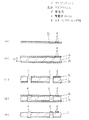
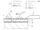
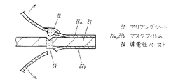
図1(a)〜(e)は本発明の第1の実施の形態における回路基板の製造方法の一部工程断面図であり、図2は同実施の形態における回路基板の製造方法のマスクフィルム貼り付け概略斜視図である。
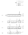
図6(a)〜(d)はそれぞれ本発明の第2の実施の形態における回路基板の製造方法の一部工程断面図、図7は同実施の形態における回路基板の製造方法および製造装置のマスクフィルム貼り付けとスキージクリーニング部形成の概略斜視図である。
2a,2b,22a,22b マスクフィルム
3,23 貫通孔
4,24 導電性ペースト
6 スキージクリーニング部
7 隆起部
8 ラミネートロール
9 溝加工部
10 加工刃固定部取り付け部
11 摺動部
12 加工刃固定部
13 加工刃
14 加工刃固定ネジ
15 ペースト充填エリア
16 製品エリア
25a,25b 金属箔
30 版
31 版枠
32 マスク
33 開口部
34 傾斜部
35 ステージ
36a 往側スキージ
36b 復側スキージ
Claims (20)
- 所定位置に隆起した隆起部を備えたスキージクリーニング部を形成したマスクフィルムを基板材料に貼り付ける工程と、それに貫通孔を設ける工程と、前記貫通孔に導電性ペーストをスキージング法にて充填する工程を備えた回路基板の製造方法。
- マスクフィルムを基板材料の両面に貼り付ける工程と、それに貫通孔を設ける工程と、前記貫通孔に導電性ペーストをスキージング法にて充填する充填工程を備え、充填工程直前までに、前記マスクフィルムの所定位置に隆起した隆起部を備えたスキージクリーニング部を形成する工程を備えた回路基板の製造方法。
- 所定位置は、導電性ペースト充填側の(マスクフィルム)製品エリア不要部もしくは製品エリア外で、かつ印刷範囲内であることを特徴とする請求項1または請求項2に記載の回路基板の製造方法。
- スキージクリーニング部は、マスクフィルムに設けた千鳥状の貫通孔であることを特徴とする請求項1に記載の回路基板の製造方法。
- スキージクリーニング部は、マスクフィルムの充填面に設けた直線状の非貫通溝であることを特徴とする請求項1または請求項2に記載の回路基板の製造方法。
- 直線状の非貫通溝を複数本設けた請求項5に記載の回路基板の製造方法。
- マスクフィルムの非貫通溝は、切削刃を用いて加工されることを特徴とする請求項5に記載の回路基板の製造方法。
- 切削刃は丸刃であることを特徴とする請求項7に記載の回路基板の製造方法。
- 丸刃は、所定の荷重で上下摺動機能を備えた加工刃固定部に回転しないように取り付けられていることを特徴とする請求項8に記載の回路基板の製造方法。
- スキージクリーニング部の加工溝の深さおよび隆起高さは、丸刃の刃先角度と荷重で調整することにより設定されることを特徴とする請求項9に記載の回路基板の製造方法。
- 隆起部の高さは少なくとも3μmである請求項1または請求項2に記載の回路基板の製造方法。
- 基板材料が織布あるいは不織布に熱硬化性樹脂を主体とする樹脂材料を含浸しBステージ化したプリプレグであることを特徴とする請求項1または請求項2に記載の回路基板の製造方法。
- 織布あるいは不織布がアラミド繊維を主体としてなることを特徴とする請求項1または請求項2に記載の回路基板の製造方法。
- 織布あるいは不織布がガラス繊維を主体としてなることを特徴とする請求項1または請求項2に記載の回路基板の製造方法。
- 貫通孔に導電性ペーストをスキージング法にて充填する工程は、回路基板上にスキージを往復させて導電性ペーストを貫通孔に充填するものであって、スキージクリーニング部で前記スキージのエッジをクリーニングすることを含むことを特徴とする請求項1または請求項2に記載の回路基板の製造方法。
- 基板材料を搬送する搬送手段と、前記搬送手段を介して上下に位置するマスクフィルムの供給手段とラミネートロールを備え、ラミネートロール後方かつ搬送手段の上方にマスクフィルムの溝加工部を備え、
前記溝加工部は、特定の刃先角度を有する加工刃を備えた加工刃固定部と、摺動部を配置した加工刃固定部取り付け部からなり、加工刃固定部は加工刃固定部取り付け部の摺動部で上下方向に摺動可能であり、
前記加工刃は加工刃固定ネジで前記加工刃固定部に取り付けられるものであり、
前記加工刃固定部の総重量は調整可能であることを特徴とする回路基板の製造装置。 - 加工刃は丸刃であり、かつ加工刃固定部に回転しないように取り付けられていることを特徴とする請求項16に記載の回路基板の製造装置。
- 溝加工部は、搬送手段の上方の位置において、位置決め固定が可能であることを特徴とする請求項16に記載の回路基板の製造装置。
- 溝加工部の直下かつ搬送手段の下方の位置に、受けロールを備えていることを特徴とする請求項16に記載の回路基板の製造装置。
- 加工刃の特定の刃先角度は、30〜90°の範囲であることを特徴とする請求項16に記載の回路基板の製造装置。
Priority Applications (7)
| Application Number | Priority Date | Filing Date | Title |
|---|---|---|---|
| JP2003433147A JP3972902B2 (ja) | 2003-12-26 | 2003-12-26 | 回路基板の製造方法および製造装置 |
| PCT/JP2004/018693 WO2005065001A1 (ja) | 2003-12-26 | 2004-12-15 | 回路基板の製造方法および製造装置 |
| US10/540,606 US8211494B2 (en) | 2003-12-26 | 2004-12-15 | Method and apparatus for manufacturing circuit board |
| KR1020057013177A KR100655731B1 (ko) | 2003-12-26 | 2004-12-15 | 회로 기판의 제조 방법 및 제조 장치 |
| CNB2004800021657A CN100482045C (zh) | 2003-12-26 | 2004-12-15 | 电路基板的制造方法以及制造装置 |
| EP04807052A EP1587351A4 (en) | 2003-12-26 | 2004-12-15 | METHOD AND DEVICE FOR PRODUCING A CONDUCTOR PLATE |
| TW093139192A TW200526101A (en) | 2003-12-26 | 2004-12-16 | Method and apparatus for manufacturing circuit board |
Applications Claiming Priority (1)
| Application Number | Priority Date | Filing Date | Title |
|---|---|---|---|
| JP2003433147A JP3972902B2 (ja) | 2003-12-26 | 2003-12-26 | 回路基板の製造方法および製造装置 |
Publications (2)
| Publication Number | Publication Date |
|---|---|
| JP2005191410A JP2005191410A (ja) | 2005-07-14 |
| JP3972902B2 true JP3972902B2 (ja) | 2007-09-05 |
Family
ID=34736504
Family Applications (1)
| Application Number | Title | Priority Date | Filing Date |
|---|---|---|---|
| JP2003433147A Expired - Fee Related JP3972902B2 (ja) | 2003-12-26 | 2003-12-26 | 回路基板の製造方法および製造装置 |
Country Status (7)
| Country | Link |
|---|---|
| US (1) | US8211494B2 (ja) |
| EP (1) | EP1587351A4 (ja) |
| JP (1) | JP3972902B2 (ja) |
| KR (1) | KR100655731B1 (ja) |
| CN (1) | CN100482045C (ja) |
| TW (1) | TW200526101A (ja) |
| WO (1) | WO2005065001A1 (ja) |
Families Citing this family (8)
| Publication number | Priority date | Publication date | Assignee | Title |
|---|---|---|---|---|
| DE102005011545A1 (de) * | 2005-03-10 | 2006-09-21 | Lpkf Laser & Electronics Ag | Verfahren zur Kontaktierung von Leiterbahnen einer Leiterplatte |
| JP2011049664A (ja) * | 2009-08-25 | 2011-03-10 | Seiko Instruments Inc | パッケージの製造方法、圧電振動子の製造方法、発振器、電子機器および電波時計 |
| NL2003627C2 (en) * | 2009-10-12 | 2011-04-13 | Stork Prints Bv | Screen printing. |
| CN103517558B (zh) * | 2012-06-20 | 2017-03-22 | 碁鼎科技秦皇岛有限公司 | 封装基板制作方法 |
| KR101527941B1 (ko) * | 2015-03-17 | 2015-06-11 | 김창열 | 다층 구조의 반도체 디바이스 테스트 보드의 수리방법 |
| CN107264008B (zh) * | 2017-07-05 | 2019-07-16 | 京东方科技集团股份有限公司 | 一种印刷掩膜板及胶液图案的印刷方法 |
| JP2023528134A (ja) | 2020-04-23 | 2023-07-04 | エルジー イノテック カンパニー リミテッド | Oled画素蒸着のための金属材質の蒸着用マスク及び蒸着用マスクの製造方法 |
| CN111629519B (zh) * | 2020-05-18 | 2021-04-09 | 微智医疗器械有限公司 | 芯片与电路板的连接方法、电路板组件及电子设备 |
Family Cites Families (15)
| Publication number | Priority date | Publication date | Assignee | Title |
|---|---|---|---|---|
| JPS57103862A (en) * | 1980-12-19 | 1982-06-28 | Fuji Xerox Co Ltd | Heat sensitive recording head |
| JPS57103862U (ja) * | 1980-12-19 | 1982-06-26 | ||
| JP2629067B2 (ja) | 1990-10-11 | 1997-07-09 | 東洋インキ製造株式会社 | モノアゾレーキ顔料および印刷インキ組成物 |
| JPH05177811A (ja) * | 1992-01-06 | 1993-07-20 | Furukawa Electric Co Ltd:The | 印刷マスクのクリーニング方法およびその装置 |
| JP2601128B2 (ja) | 1992-05-06 | 1997-04-16 | 松下電器産業株式会社 | 回路形成用基板の製造方法および回路形成用基板 |
| JPH05338370A (ja) * | 1992-06-10 | 1993-12-21 | Dainippon Screen Mfg Co Ltd | スクリーン印刷用メタルマスク版 |
| JP2768236B2 (ja) | 1993-10-08 | 1998-06-25 | 松下電器産業株式会社 | 多層基板の製造方法 |
| DE69737281T2 (de) * | 1996-12-10 | 2007-12-20 | Matsushita Electric Industrial Co., Ltd., Kadoma | Vorrichtung und Verfahren zum Drucken von Lötpaste |
| JP3533596B2 (ja) * | 1999-06-25 | 2004-05-31 | 日本特殊陶業株式会社 | 配線基板の製造方法 |
| JP3459380B2 (ja) * | 1999-06-30 | 2003-10-20 | 日本特殊陶業株式会社 | プリント配線板の製造方法及びマスク |
| JP3292194B2 (ja) * | 2000-02-01 | 2002-06-17 | 松下電器産業株式会社 | 印刷用版およびそれを用いた印刷方法 |
| US6638363B2 (en) * | 2000-11-22 | 2003-10-28 | Gunter Erdmann | Method of cleaning solder paste |
| JP3721982B2 (ja) | 2000-12-04 | 2005-11-30 | 松下電器産業株式会社 | 回路形成基板の製造方法および回路形成基板の製造装置 |
| JP2003033967A (ja) * | 2001-07-23 | 2003-02-04 | Pearl Kogyo Kk | 樹脂材の加工方法及び加工装置 |
| US7105277B2 (en) * | 2002-09-24 | 2006-09-12 | Matsushita Electric Industrial Co., Ltd. | Printing plate, circuit board and method of printing circuit board |
-
2003
- 2003-12-26 JP JP2003433147A patent/JP3972902B2/ja not_active Expired - Fee Related
-
2004
- 2004-12-15 EP EP04807052A patent/EP1587351A4/en not_active Withdrawn
- 2004-12-15 KR KR1020057013177A patent/KR100655731B1/ko not_active Expired - Fee Related
- 2004-12-15 CN CNB2004800021657A patent/CN100482045C/zh not_active Expired - Fee Related
- 2004-12-15 WO PCT/JP2004/018693 patent/WO2005065001A1/ja not_active Ceased
- 2004-12-15 US US10/540,606 patent/US8211494B2/en not_active Expired - Fee Related
- 2004-12-16 TW TW093139192A patent/TW200526101A/zh not_active IP Right Cessation
Also Published As
| Publication number | Publication date |
|---|---|
| KR100655731B1 (ko) | 2006-12-11 |
| TW200526101A (en) | 2005-08-01 |
| EP1587351A1 (en) | 2005-10-19 |
| TWI335196B (ja) | 2010-12-21 |
| US8211494B2 (en) | 2012-07-03 |
| EP1587351A4 (en) | 2009-04-01 |
| US20060115583A1 (en) | 2006-06-01 |
| JP2005191410A (ja) | 2005-07-14 |
| WO2005065001A1 (ja) | 2005-07-14 |
| CN1739322A (zh) | 2006-02-22 |
| CN100482045C (zh) | 2009-04-22 |
| KR20060006998A (ko) | 2006-01-23 |
Similar Documents
| Publication | Publication Date | Title |
|---|---|---|
| JP3292194B2 (ja) | 印刷用版およびそれを用いた印刷方法 | |
| JP3972902B2 (ja) | 回路基板の製造方法および製造装置 | |
| CN1318228C (zh) | 印刷用版、电路基板以及对电路基板的印刷方法 | |
| JP2768236B2 (ja) | 多層基板の製造方法 | |
| KR100748208B1 (ko) | 연성회로기판의 라미네이팅 장치 및 그 방법 | |
| CN101048031B (zh) | 印刷用版、电路基板以及对电路基板的印刷方法 | |
| JP2011031507A (ja) | 印刷用版 | |
| JP3654279B2 (ja) | 回路基板および回路基板への印刷方法 | |
| CN1698403B (zh) | 基板的制造方法 | |
| JP4395741B2 (ja) | 多層基板の製造方法 | |
| JP5124977B2 (ja) | ペースト充填方法 | |
| CN119562452B (zh) | 一种电路板台阶槽处理方法 | |
| KR102918802B1 (ko) | 전자파 흡수 복합소재 제조장치 | |
| JP4465962B2 (ja) | 基板の製造方法 | |
| JP5011784B2 (ja) | 印刷用版およびそれを用いた印刷方法 | |
| JPH11238958A (ja) | 回路基板の製造方法及び製造装置 | |
| JP2009234223A (ja) | 銅張積層板およびこれを用いた配線基板の製造方法ならびに銅張積層板の端面処理方法およびこれに用いる端面処理装置 | |
| JP2003158366A (ja) | 回路形成基板の製造装置とそれを用いた回路形成基板の製造方法 | |
| JP2015002311A (ja) | プリント配線板の製造方法およびプリント配線板用ペースト充填機 | |
| JPH0473147A (ja) | 積層板の製造装置 | |
| JPH0473146A (ja) | 積層板の製造装置 |
Legal Events
| Date | Code | Title | Description |
|---|---|---|---|
| RD01 | Notification of change of attorney |
Free format text: JAPANESE INTERMEDIATE CODE: A7421 Effective date: 20050708 |
|
| A131 | Notification of reasons for refusal |
Free format text: JAPANESE INTERMEDIATE CODE: A131 Effective date: 20070306 |
|
| A521 | Request for written amendment filed |
Free format text: JAPANESE INTERMEDIATE CODE: A523 Effective date: 20070424 |
|
| TRDD | Decision of grant or rejection written | ||
| A01 | Written decision to grant a patent or to grant a registration (utility model) |
Free format text: JAPANESE INTERMEDIATE CODE: A01 Effective date: 20070522 |
|
| A61 | First payment of annual fees (during grant procedure) |
Free format text: JAPANESE INTERMEDIATE CODE: A61 Effective date: 20070604 |
|
| FPAY | Renewal fee payment (event date is renewal date of database) |
Free format text: PAYMENT UNTIL: 20100622 Year of fee payment: 3 |
|
| FPAY | Renewal fee payment (event date is renewal date of database) |
Free format text: PAYMENT UNTIL: 20100622 Year of fee payment: 3 |
|
| FPAY | Renewal fee payment (event date is renewal date of database) |
Free format text: PAYMENT UNTIL: 20110622 Year of fee payment: 4 |
|
| FPAY | Renewal fee payment (event date is renewal date of database) |
Free format text: PAYMENT UNTIL: 20120622 Year of fee payment: 5 |
|
| FPAY | Renewal fee payment (event date is renewal date of database) |
Free format text: PAYMENT UNTIL: 20120622 Year of fee payment: 5 |
|
| FPAY | Renewal fee payment (event date is renewal date of database) |
Free format text: PAYMENT UNTIL: 20130622 Year of fee payment: 6 |
|
| LAPS | Cancellation because of no payment of annual fees |