JP3972902B2 - Circuit board manufacturing method and manufacturing apparatus - Google Patents
Circuit board manufacturing method and manufacturing apparatus Download PDFInfo
- Publication number
- JP3972902B2 JP3972902B2 JP2003433147A JP2003433147A JP3972902B2 JP 3972902 B2 JP3972902 B2 JP 3972902B2 JP 2003433147 A JP2003433147 A JP 2003433147A JP 2003433147 A JP2003433147 A JP 2003433147A JP 3972902 B2 JP3972902 B2 JP 3972902B2
- Authority
- JP
- Japan
- Prior art keywords
- circuit board
- manufacturing
- mask film
- squeegee
- conductive paste
- Prior art date
- Legal status (The legal status is an assumption and is not a legal conclusion. Google has not performed a legal analysis and makes no representation as to the accuracy of the status listed.)
- Expired - Fee Related
Links
Images


Classifications
-
- H—ELECTRICITY
- H05—ELECTRIC TECHNIQUES NOT OTHERWISE PROVIDED FOR
- H05K—PRINTED CIRCUITS; CASINGS OR CONSTRUCTIONAL DETAILS OF ELECTRIC APPARATUS; MANUFACTURE OF ASSEMBLAGES OF ELECTRICAL COMPONENTS
- H05K3/00—Apparatus or processes for manufacturing printed circuits
- H05K3/40—Forming printed elements for providing electric connections to or between printed circuits
- H05K3/4038—Through-connections; Vertical interconnect access [VIA] connections
- H05K3/4053—Through-connections; Vertical interconnect access [VIA] connections by thick-film techniques
- H05K3/4069—Through-connections; Vertical interconnect access [VIA] connections by thick-film techniques for via connections in organic insulating substrates
-
- H—ELECTRICITY
- H05—ELECTRIC TECHNIQUES NOT OTHERWISE PROVIDED FOR
- H05K—PRINTED CIRCUITS; CASINGS OR CONSTRUCTIONAL DETAILS OF ELECTRIC APPARATUS; MANUFACTURE OF ASSEMBLAGES OF ELECTRICAL COMPONENTS
- H05K2201/00—Indexing scheme relating to printed circuits covered by H05K1/00
- H05K2201/03—Conductive materials
- H05K2201/0332—Structure of the conductor
- H05K2201/0335—Layered conductors or foils
- H05K2201/0355—Metal foils
-
- H—ELECTRICITY
- H05—ELECTRIC TECHNIQUES NOT OTHERWISE PROVIDED FOR
- H05K—PRINTED CIRCUITS; CASINGS OR CONSTRUCTIONAL DETAILS OF ELECTRIC APPARATUS; MANUFACTURE OF ASSEMBLAGES OF ELECTRICAL COMPONENTS
- H05K2201/00—Indexing scheme relating to printed circuits covered by H05K1/00
- H05K2201/09—Shape and layout
- H05K2201/09009—Substrate related
- H05K2201/09036—Recesses or grooves in insulating substrate
-
- H—ELECTRICITY
- H05—ELECTRIC TECHNIQUES NOT OTHERWISE PROVIDED FOR
- H05K—PRINTED CIRCUITS; CASINGS OR CONSTRUCTIONAL DETAILS OF ELECTRIC APPARATUS; MANUFACTURE OF ASSEMBLAGES OF ELECTRICAL COMPONENTS
- H05K2201/00—Indexing scheme relating to printed circuits covered by H05K1/00
- H05K2201/09—Shape and layout
- H05K2201/09209—Shape and layout details of conductors
- H05K2201/09654—Shape and layout details of conductors covering at least two types of conductors provided for in H05K2201/09218 - H05K2201/095
- H05K2201/09781—Dummy conductors, i.e. not used for normal transport of current; Dummy electrodes of components
-
- H—ELECTRICITY
- H05—ELECTRIC TECHNIQUES NOT OTHERWISE PROVIDED FOR
- H05K—PRINTED CIRCUITS; CASINGS OR CONSTRUCTIONAL DETAILS OF ELECTRIC APPARATUS; MANUFACTURE OF ASSEMBLAGES OF ELECTRICAL COMPONENTS
- H05K2203/00—Indexing scheme relating to apparatus or processes for manufacturing printed circuits covered by H05K3/00
- H05K2203/01—Tools for processing; Objects used during processing
- H05K2203/0191—Using tape or non-metallic foil in a process, e.g. during filling of a hole with conductive paste
-
- H—ELECTRICITY
- H05—ELECTRIC TECHNIQUES NOT OTHERWISE PROVIDED FOR
- H05K—PRINTED CIRCUITS; CASINGS OR CONSTRUCTIONAL DETAILS OF ELECTRIC APPARATUS; MANUFACTURE OF ASSEMBLAGES OF ELECTRICAL COMPONENTS
- H05K2203/00—Indexing scheme relating to apparatus or processes for manufacturing printed circuits covered by H05K3/00
- H05K2203/02—Details related to mechanical or acoustic processing, e.g. drilling, punching, cutting, using ultrasound
- H05K2203/0228—Cutting, sawing, milling or shearing
-
- H—ELECTRICITY
- H05—ELECTRIC TECHNIQUES NOT OTHERWISE PROVIDED FOR
- H05K—PRINTED CIRCUITS; CASINGS OR CONSTRUCTIONAL DETAILS OF ELECTRIC APPARATUS; MANUFACTURE OF ASSEMBLAGES OF ELECTRICAL COMPONENTS
- H05K2203/00—Indexing scheme relating to apparatus or processes for manufacturing printed circuits covered by H05K3/00
- H05K2203/06—Lamination
- H05K2203/063—Lamination of preperforated insulating layer
-
- H—ELECTRICITY
- H05—ELECTRIC TECHNIQUES NOT OTHERWISE PROVIDED FOR
- H05K—PRINTED CIRCUITS; CASINGS OR CONSTRUCTIONAL DETAILS OF ELECTRIC APPARATUS; MANUFACTURE OF ASSEMBLAGES OF ELECTRICAL COMPONENTS
- H05K2203/00—Indexing scheme relating to apparatus or processes for manufacturing printed circuits covered by H05K3/00
- H05K2203/14—Related to the order of processing steps
- H05K2203/1461—Applying or finishing the circuit pattern after another process, e.g. after filling of vias with conductive paste, after making printed resistors
Description
本発明は、各種電子機器に使用される両面あるいは多層配線基板などに用いられるペーストのパターンあるいは貫通孔への充填等に用いられる回路基板の製造方法およびその製造装置に関するものである。 The present invention relates to a method of manufacturing a circuit board used for filling a pattern or a through hole of a paste used for double-sided or multilayer wiring boards used in various electronic devices, and a manufacturing apparatus therefor.
近年、電子機器の小型化、高密度化に伴い、産業用にとどまらず民生用の分野においても回路基板の多層化が強く要望されるようになってきた。 In recent years, with the downsizing and increasing the density of electronic devices, there has been a strong demand for multilayer circuit boards not only for industrial use but also for consumer use.
このような回路基板では、複数層の回路パターンの間をインナービアホール接続する接続方法および信頼度の高い構造の新規開発が不可欠なものになっているが、導電性ペーストによりインナービアホール接続した新規な構成の高密度の回路基板製造法が提案されている。 In such a circuit board, it is indispensable to newly develop a connection method for connecting inner via holes between circuit patterns of a plurality of layers and a highly reliable structure. Proposed high density circuit board manufacturing methods have been proposed.
以下従来の両面の回路基板の製造方法について説明する。 Hereinafter, a conventional method for manufacturing a double-sided circuit board will be described.
図10(a)〜(f)は従来の回路基板の製造方法の工程断面図、図11は従来例の開口部を有するマスクを取り付けた版枠を示す斜視図、図12は従来例の開口部を有するマスクを取り付けた版枠の断面図、図13(a)〜(g)はスキージング法によるペースト充填の工程断面図、図14は従来例の回路基板を用いたペースト充填時の一部断面図である。 10 (a) to 10 (f) are process sectional views of a conventional method of manufacturing a circuit board, FIG. 11 is a perspective view showing a plate frame attached with a mask having an opening of a conventional example, and FIG. 12 is an opening of the conventional example. 13A to 13G are cross-sectional views of a paste filling process using a squeezing method, and FIG. 14 illustrates a paste filling process using a conventional circuit board. FIG.
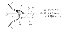
図10において、21は300mm×500mm、厚さ約150μmのプリプレグシートであり、例えば不織布の全芳香族ポリアミド繊維に熱硬化性エポキシ樹脂を含浸させた複合材からなる基材が用いられる。22a,22bはマスクフィルムでありプリプレグシート21と接着する面に0.01μm以下の厚みでSi系の離型層部を形成した厚さ約20μm、幅300mmのプラスチックフィルム、例えばポリエチレンテレフタレートが用いられる。
In FIG. 10,
プリプレグシート21とマスクフィルム22a,22bの張り合わせはラミネート装置を用いてプリプレグシート21の樹脂成分を溶融させてマスクフィルム22a,22bが連続的に接着する方法が提案されている。23は貫通孔であり、プリプレグシート21の両面に貼り付ける厚さ35μmの銅などの金属箔25a,25bと電気的に接続する導電性ペースト24が充填されている。
For the pasting of the
回路基板の製造は、まず、両面にマスクフィルム22a,22bが接着されたプリプレグシート21(図10(a))の所定の箇所に図10(b)に示すようにレーザ加工法などを利用して貫通孔23が形成される。
The circuit board is manufactured by using a laser processing method or the like as shown in FIG. 10 (b) at a predetermined position of the prepreg sheet 21 (FIG. 10 (a)) having the
次に図10(c)に示すように、貫通孔23に導電性ペースト24が充填される。導電性ペースト24を充填する方法としては、貫通孔23を有するプリプレグシート21を一般の印刷機(図示せず)のステージ上に設置し、ウレタンゴムなどの2本のスキージを交互に用いて往復させることで直接導電性ペースト24がマスクフィルム22aの上から充填される。このとき、上面のマスクフィルム22a,22bは印刷マスクの役割と、プリプレグシート21の表面の汚染防止の役割を果たしている。
Next, as shown in FIG. 10C, the through-
導電性ペースト24の充填方法について図11、図12、図13(a)〜(g)を用いてさらに説明する。
The filling method of the
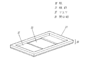
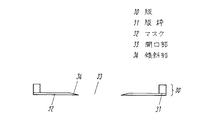
導電性ペースト24の充填にはスキージング法が用いられているが、プリプレグシート21には専用のマスクフィルム22a,22bが配置されているため、図11、図12に示すように充填用の版30の版枠31にはプリプレグシート21のペースト充填有効面積より広い250mm×450mmの開口部33を設けた厚さ約3mmのステンレス製のマスク32が取り付けられている。
A squeezing method is used for filling the
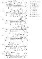
導電性ペースト24の充填は、まず、図13(a)に示すように印刷機(図示せず)のステージ35に置載した両面にマスクフィルムが接着され、貫通孔23が形成されたプリプレグシート21にマスク32がセットされる。
First, as shown in FIG. 13A, the
次に、上方に設けられた上下左右に移動・加圧可能な往側スキージ36aと復側スキージ36bのうち往側スキージ36aのみをマスク32上の所定位置に降下させ、圧力をかけて導電性ペースト24をローリングさせながら前進させている。
Next, only the forward squeegee 36a of the forward squeegee 36a and the backward
次に図13(b)に示すように、マスク32の傾斜部34を通過してプリプレグシート21上に到達する。往復のスキージ36a,36bは圧力を保持しながら位置に応じて自由に上下可能な機能を有している。
Next, as shown in FIG. 13 (b), it passes through the
次に図13(c)に示すように、往側スキージ36aはプリプレグシート21上と再度マスク32の傾斜部を通過してマスク32上の定位置でストップした後、上昇させて導電性ペースト24を自然落下させている。
Next, as shown in FIG. 13 (c), the forward squeegee 36 a passes over the
次に図13(d)に示すように、復側スキージ36bのみをマスク32上の所定位置に下降させる。その後図13(e)〜(g)に示すように往側スキージ36aと同様に復側スキージ36bをマスク32とプリプレグ21上を通過させることで貫通孔23への導電性ペースト24の充填が完了する。
Next, as shown in FIG. 13 (d), only the return-
そして図10(d)に示すように、プリプレグシート21の両面からマスクフィルム22a,22bを剥離する。
Then, as shown in FIG. 10 (d), the
次に図10(e)に示すように、プリプレグシート21の両面に銅などの金属箔25a,25bを重ねる。
Next, as shown in FIG. 10 (e),
この状態で熱プレスで加熱加圧することにより、図10(f)に示すように、プリプレグシート21の厚みが圧縮される(t2=約100μm)とともにプリプレグシート21と金属箔25a,25bとが接着され、両面の金属箔25a,25bは所定位置に設けた貫通孔23に充填された導電性ペースト24により電気的に接続されている。
By heating and pressurizing with a hot press in this state, the thickness of the
そして、両面の金属箔25a,25bを選択的にエッチングして回路パターンが形成され(図示せず)て両面の回路基板が得られる。
Then, the
なお、この出願の発明に関連する先行技術文献情報としては、例えば、特許文献1、特許文献2が知られている。
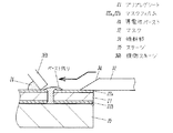
しかしながら上記の従来のペースト充填法における課題を図14に示す。 However, the problem in the conventional paste filling method is shown in FIG.
すなわち(導電性ペースト24粘度が高い場合)、印刷を開始する際、マスク32の傾斜部34を下降した時に、導電性ペースト24がプリプレグシート21面に押しつけられ、これによってスキージ36bエッジ周辺のペースト中の樹脂成分が押し出され、スキージ36bエッジ全面により高粘度の導電性ペースト24が固着する。
That is (when the viscosity of the
この固着した導電性ペースト24がプリプレグシート21に形成された貫通孔23を通過する際、特にスキージ36bのペースト充填幅全面で、かつスキージ進行方向の最初での貫通孔23上に堅いペーストが残りやすく、特にマスクフィルム厚みを20μmとした場合、貫通孔23の直径が150μm以下になると図15に示すようにマスクフィルム22a,22bを剥がす際に、導電性ペースト24の一部がマスクフィルム22a側に取られて貫通孔23内の導電性ペースト24が不足することで接続品質に影響を及ぼす場合があるという問題があった。
When this fixed
本発明は上記従来の課題を解決するもので、プリプレグシートからのマスクフィルム剥離時の導電性ペースト取られを防止して接続品質に優れた回路基板を提供することを目的とするものである。 SUMMARY OF THE INVENTION An object of the present invention is to solve the above-described conventional problems, and to provide a circuit board excellent in connection quality by preventing the conductive paste from being removed when the mask film is peeled from the prepreg sheet.
上記目的を達成するために、本発明の回路基板の製造方法および回路基板へのペースト充填方法は、製品の貫通孔をスキージが通過する前に、回路基板上に設けたスキージクリーニング部を通過させてスキージエッジの高粘度のペーストを除去するもので接続品質に優れた回路基板が得られる。 In order to achieve the above object, the circuit board manufacturing method and circuit board paste filling method of the present invention allow a squeegee cleaning section provided on the circuit board to pass before the squeegee passes through the through hole of the product. By removing the high-viscosity paste from the squeegee edge, a circuit board with excellent connection quality can be obtained.
本発明の請求項1に記載の発明は、特にあらかじめ導電性ペースト充填面のマスクフィルムに隆起した隆起部を備えたスキージクリーニング部を形成しておくことで、高粘度の導電性ペーストは、クリーニング部で除去される。これにより、前記スキージクリーニング部以降の貫通孔上には余分な導電性ペースト残りがなくなり安定した接続品質が得られるという作用効果が得られる。 According to the first aspect of the present invention, a high-viscosity conductive paste is formed by forming a squeegee cleaning portion having a raised portion on the mask film on the conductive paste filling surface in advance. Removed in the part. As a result, there is obtained an operational effect that there is no excess conductive paste remaining on the through-holes after the squeegee cleaning portion, and a stable connection quality can be obtained.
また、マスクフィルム単独でスキージクリーニング部の形成が可能となるため、マスクフィルム作成からプリプレグシートへの貼り付け直前までに形成すればよいことになり、効率の高い加工方法を選択できるという作用を有する。 In addition, since the squeegee cleaning part can be formed by using the mask film alone, it is sufficient to form the mask film from the creation of the mask film to immediately before being attached to the prepreg sheet, and it is possible to select an efficient processing method. .
本発明の請求項2に記載の発明は、特にプリプレグシートへのマスクフィルム貼り付けからペースト充填までに導電性ペースト充填面のマスクフィルムに隆起した隆起部を備えたスキージクリーニング部を形成することで、高粘度の導電性ペーストはクリーニング部で除去される。これにより、前記スキージクリーニング部以降の貫通孔上には余分な導電性ペースト残りがなくなり安定した接続品質が得られるという作用効果が得られる。 The invention according to claim 2 of the present invention is to form a squeegee cleaning portion having a raised portion raised on the mask film on the conductive paste filling surface, particularly from the pasting of the mask film to the prepreg sheet to the filling of the paste. The high-viscosity conductive paste is removed by the cleaning unit. As a result, there is obtained an operational effect that there is no excess conductive paste remaining on the through-holes after the squeegee cleaning portion, and a stable connection quality can be obtained.
また、導電性ペースト充填や貫通孔加工時の位置決めのベースとなるプリプレグシートにマスクフィルム貼り付け後にスキージクリーニング部を形成することから、スキージクリーニング形成時の位置決めが容易になるという作用を有する。 In addition, since the squeegee cleaning portion is formed after the mask film is attached to the prepreg sheet that serves as a positioning base for filling with conductive paste and through-hole processing, positioning at the time of forming the squeegee cleaning is facilitated.
特に、スキージクリーニング部に形成した隆起部がスキージエッジの高粘度の導電性ペーストを掻き取って除去することでスキージクリーニングを確実なものにできるという作用効果が得られる。 In particular, the squeegee cleaning can be reliably performed by removing the high-viscosity conductive paste on the squeegee edge by the raised portion formed in the squeegee cleaning unit.
本発明の請求項3に記載の発明は、特に導電性ペースト充填側のマスクフィルムの製品エリア不要部もしくは製品エリア外で、かつ印刷範囲内の所定位置にスキージクリーニング部を形成することで製品内の貫通孔をスキージが通過する前にスキージ高粘度の導電性ペーストはクリーニング部で除去され、製品内の貫通孔上には余分な導電性ペースト残りはなくなり安定した接続品質が得られるという作用効果が得られる。 According to the third aspect of the present invention, in particular, the squeegee cleaning part is formed in a predetermined position within the printing range outside the product area or outside the product area of the mask film on the conductive paste filling side. The squeegee high-viscosity conductive paste is removed by the cleaning part before the squeegee passes through the through-hole of the squeegee, and there is no excess conductive paste remaining on the through-hole in the product, so that stable connection quality can be obtained. Is obtained.
本発明の請求項4に記載の発明は、特にマスクフィルムに貫通孔のスキージクリーニング部を形成する際に貫通孔間が繋がって破断させずに、疑似直線にできるという作用効果が得られる。 The invention according to claim 4 of the present invention has an effect that a quasi-straight line can be obtained without connecting and breaking the through-holes when the through-hole squeegee cleaning portion is formed on the mask film.
本発明の請求項5に記載の発明は、特にスキージクリーニング部を非貫通の溝とすることで加工面積が小さくなるとともに、マスクフィルム剥離後に不要な導電性ペーストがプリプレグシート上に残らないという作用効果が得られる。 The invention according to claim 5 of the present invention has an effect that the processing area is reduced by making the squeegee cleaning part a non-penetrating groove, and unnecessary conductive paste does not remain on the prepreg sheet after the mask film is peeled off. An effect is obtained.
本発明の請求項6に記載の発明は、特にスキージクリーニング部を複数本形成したことでペースト充填時のプリプレグシートの位置決めばらつきなどの影響を吸収するとともに、スキージクリーニング効果をより確実なものにできるという作用効果が得られる。
The invention according to
本発明の請求項7に記載の発明は、特にスキージクリーニング部形成に切削刃を用いたことで形成した隆起部がスキージエッジの高粘度の導電性ペーストを掻き取って除去することでスキージクリーニングを確実なものにできるという作用効果が得られる。
In the invention according to
本発明の請求項8に記載の発明は、特に切削刃に丸刃を設けたことで、切削時の接触面積が大きくなり、押し圧による切削深さへの影響度を小さくできるとともに、切削位置の移動が回転でできるため容易となるという作用効果が得られる。 In the invention according to claim 8 of the present invention, in particular, the cutting blade is provided with a round blade, so that the contact area at the time of cutting is increased, the degree of influence of the pressing force on the cutting depth can be reduced, and the cutting position The effect of facilitating the movement of the lens can be obtained by rotation.
本発明の請求項9に記載の発明は、特に丸刃の固定部を所定の荷重としたことで加工深さを調整できるとともに、上下摺動機能を持たせたことで基板材料やマスクフィルムの表面凹凸に追従して溝加工ができる。さらに丸刃を非回転とすることで、点での加圧切削から面での移動による深さ方向への順次加工となり安定した溝加工ができるという作用効果が得られる。 In the invention according to claim 9 of the present invention, the processing depth can be adjusted by setting the fixed portion of the round blade to a predetermined load, and the substrate material and the mask film can be adjusted by providing a vertical sliding function. Grooves can be made following surface irregularities. Further, by making the round blade non-rotating, it is possible to obtain a working effect that a stable grooving can be performed by sequential processing in the depth direction by moving on the surface from pressure cutting at a point.
本発明の請求項10に記載の発明は、特に丸刃の刃先角度と荷重でマスクフィルムの加工溝の深さおよび隆起高さを調整したことで安定した溝深さと隆起高さが得られ、スキージクリーニング効果を安定させるという作用効果が得られる。 In the invention according to claim 10 of the present invention, a stable groove depth and a raised height can be obtained by adjusting the depth and raised height of the processed groove of the mask film, in particular, with the blade edge angle and load of the round blade, The effect of stabilizing the squeegee cleaning effect can be obtained.
本発明の請求項11に記載の発明は、特にマスクフィルムの隆起高さを3μm以上としたことで安定した溝深さと隆起高さが得られ、スキージクリーニング効果を安定させるという作用効果が得られる。 According to the eleventh aspect of the present invention, a stable groove depth and a raised height can be obtained particularly by setting the raised height of the mask film to 3 μm or more, and an effect of stabilizing the squeegee cleaning effect can be obtained. .
本発明の請求項12に記載の発明は、特に基板材料が織布あるいは不織布に熱硬化性樹脂を主体とする樹脂材料を含浸しBステージ化したプリプレグが好ましく、請求項1または請求項2に記載する本発明の効果が得られるという作用効果が得られる。
The invention described in
本発明の請求項13に記載の発明は、特に織布あるいは不織布がアラミド繊維を主体としてなることが好ましく、請求項1または請求項2に記載する本発明の効果が得られるという作用効果が得られる。
In the invention according to claim 13 of the present invention, it is particularly preferable that the woven or non-woven fabric is mainly composed of aramid fibers, and the effect of obtaining the effect of the present invention described in
本発明の請求項14に記載の発明は、織布あるいは不織布がガラス繊維を主体としてなることが好ましく、請求項1または請求項2に記載の本発明の効果が得られるという作用効果が得られる。
In the invention described in
本発明の請求項15に記載の発明は、特に印刷する前に回路基板に設けたスキージクリーニング部でスキージエッジをクリーニングする回路基板への印刷方法とすることで高粘度の導電性ペーストはクリーニング部で除去されて、製品内の貫通孔上には余分な導電性ペースト残りがないため、プリプレグシートからのマスクフィルム剥離時の導電性ペースト取られがなくなり接続品質に優れた回路基板が得られるという作用効果が得られる。 According to the fifteenth aspect of the present invention, a highly viscous conductive paste is formed in a cleaning part by using a printing method on a circuit board in which a squeegee edge is cleaned by a squeegee cleaning part provided on the circuit board before printing. Since there is no excess conductive paste remaining on the through-hole in the product, the conductive paste is not removed when the mask film is peeled off from the prepreg sheet, and a circuit board with excellent connection quality is obtained. The effect is obtained.
本発明の請求項16に記載の発明は、特にラミネートロール後方かつ搬送手段の上方にマスクフィルムの溝加工部を備え、前記溝加工部は、特定の刃先角度を有する加工刃を備えた加工刃固定部と、摺動部を配置した加工刃固定部取り付け部からなり、加工刃固定部は加工刃固定部取り付け部の摺動部で上下方向に摺動可能であり、前記加工刃は加工刃固定ネジで前記加工刃固定部に取り付けられるものであり、前記加工刃固定部の総重量は調整可能である回路基板の製造装置を提供することにより、プリプレグシートへのマスクフィルム貼り付けからペースト充填までの間に、導電性ペースト充填面のマスクフィルムにスキージクリーニング部を容易に形成することができる。 The invention according to claim 16 of the present invention is provided with a groove processing portion of a mask film, particularly behind the laminating roll and above the conveying means, and the groove processing portion includes a processing blade having a specific cutting edge angle. The processing blade fixing portion is slidable in the vertical direction by the sliding portion of the processing blade fixing portion mounting portion, and the processing blade is a processing blade. Filling paste from mask film affixing to a prepreg sheet by providing a circuit board manufacturing device that is attached to the processing blade fixing part with a fixing screw, and the total weight of the processing blade fixing part is adjustable In the meantime, the squeegee cleaning part can be easily formed on the mask film on the conductive paste filling surface.
これにより、高粘度の導電性ペーストはクリーニング部で除去され、前記スキージクリーニング部以降の貫通孔上には余分な導電性ペースト残りがなくなり安定した接続品質が得られるという作用効果が得られる。 As a result, the conductive paste having a high viscosity is removed by the cleaning unit, and there is obtained an effect that a stable connection quality can be obtained since there is no excess conductive paste remaining on the through holes after the squeegee cleaning unit.
また、加工深さを調整できるとともに、上下摺動機能を持たせたことで基板材料やマスクフィルムの表面凹凸に追従して安定した溝加工ができるという作用効果が得られる。 In addition, the working depth can be adjusted, and by providing the up-and-down sliding function, it is possible to obtain an effect that stable groove processing can be performed following the surface irregularities of the substrate material and the mask film.
本発明の請求項17に記載の発明は、特に加工刃は丸刃とし、かつ加工刃固定部に回転しないように取り付けられていることで、点での加圧切削から面での移動による深さ方向への順次加工となり安定した溝加工ができるという作用効果が得られる。 According to the seventeenth aspect of the present invention, in particular, the processing blade is a round blade and is attached to the processing blade fixing portion so as not to rotate. The effect is obtained that it is possible to perform stable grooving by sequentially processing in the vertical direction.
本発明の請求項18に記載の発明は、特に溝加工部は、位置決め固定が可能であるため、マスクフィルムを交換する毎にプリプレグシートとの位置決めをする必要はない。これにより、位置決めのバラツキもなく、精度良くスキージクリーニング部を形成でき、併せて生産性も向上させるという作用効果が得られる。 In the invention described in claim 18 of the present invention, in particular, since the grooved portion can be positioned and fixed, it is not necessary to position the prepreg sheet every time the mask film is replaced. As a result, the squeegee cleaning unit can be formed with high accuracy without variation in positioning, and an effect of improving productivity can be obtained.
本発明の請求項19に記載の発明は、特に溝加工部の直下に受けロールを備えていることによって、安定した溝加工ができるとともに受けロールが回転することでプリプレグシートへの傷を防止するという作用効果が得られる。 According to the nineteenth aspect of the present invention, by providing the receiving roll immediately below the groove processing portion, it is possible to perform stable grooving and prevent damage to the prepreg sheet by rotating the receiving roll. The effect is obtained.
本発明の請求項20に記載の発明は、特に加工刃の刃先角度を、30〜90°とし、所定の荷重を加えることにより、切削時のマスクフィルムの加工溝の深さや隆起部の高さをスキージクリーニング部に適したものとすることができるという作用効果が得られる。 In the invention according to claim 20 of the present invention, the depth of the processed groove of the mask film and the height of the raised portion at the time of cutting are particularly determined by setting the cutting edge angle of the processing blade to 30 to 90 ° and applying a predetermined load. The effect of being able to be suitable for the squeegee cleaning unit is obtained.
本発明の製造方法及び製造装置は、回路基板の貫通孔にペースト充填する前に回路基板上に設けたスキージクリーニング部でスキージエッジの高粘度のペーストを除去することで、製品の貫通孔上に高粘度のペースト残りを防止することが可能となり、品質に優れた回路基板を提供できるという効果を有する。 The manufacturing method and the manufacturing apparatus of the present invention remove the high-viscosity paste at the squeegee edge by a squeegee cleaning unit provided on the circuit board before filling the through-hole of the circuit board with the paste. It is possible to prevent a high-viscosity paste residue and to provide a circuit board with excellent quality.
本発明の回路基板の製造方法および回路基板への印刷方法は、導電性ペースト充填面のマスクフィルムの基板材料の製品エリアの不要部もしくは製品エリア外で、かつ印刷範囲内の相当位置にレーザ加工法を用いて孔周辺が隆起した直線状や千鳥状の非貫通孔あるいは千鳥状の貫通孔、もしくは切削刃を用いて形成した直線状や千鳥状の非貫通溝からなるスキージクリーニング部を形成した後、ペースト充填面と反対側のマスクフィルムとを基板材料の両面に貼り付けて貫通孔を設けた後ペースト充填する。 The method for manufacturing a circuit board and the method for printing on the circuit board according to the present invention include laser processing at an unnecessary portion of the product area of the substrate material of the mask film on the conductive paste filling surface or outside the product area and at a corresponding position within the printing range. A squeegee cleaning part consisting of straight or staggered non-through holes or staggered through holes, or straight or staggered non-through grooves formed using a cutting blade was formed using this method. Then, the paste film is pasted on the opposite side of the paste film on both sides of the substrate material to provide through holes, and then the paste is filled.
あるいは、基板材料の両面にマスクフィルムを貼り付けた直後からペースト充填直前まで導電性ペースト充填面のマスクフィルムの基板材料の製品エリアの不要部もしくは製品エリア外で、かつ印刷範囲内の相当位置にレーザ加工法を用いて孔周辺が隆起した直線状や千鳥状の非貫通孔あるいは千鳥状の貫通孔、もしくは切削刃を用いて形成した直線状や千鳥状の非貫通溝からなるスキージクリーニング部を形成してペースト充填することで、製品内の貫通孔へのペースト充填前にクリーニング部でスキージエッジ部の高粘度ペーストを除去するため製品の貫通孔への堅いペースト残りがなくなり、マスクフィルムを剥がす際に、ペーストの一部がマスクフィルム側に取られて品質に悪影響を及ぼす可能性を解消するという作用を有し、ペースト充填品質の高い回路基板の製造方法を提供するものである。 Alternatively, from immediately after the mask film is pasted on both sides of the substrate material to immediately before the paste filling, the mask film substrate material on the conductive paste filling surface is outside the product area of the substrate material or outside the product area and at a corresponding position within the printing range. A squeegee cleaning part consisting of a linear or staggered non-through hole or staggered through hole or a straight or staggered non-through groove formed with a cutting blade using a laser processing method By forming and filling the paste, the high-viscosity paste at the squeegee edge is removed at the cleaning part before filling the through-hole in the product, so there is no hard paste remaining in the through-hole of the product and the mask film is peeled off In this case, part of the paste is taken to the mask film side to eliminate the possibility of adversely affecting the quality. There is provided a method of manufacturing a high circuit board of preparative filling quality.
また、これを容易に実現するための回路基板の製造装置を提供するものである。 Further, the present invention provides a circuit board manufacturing apparatus for easily realizing this.
以下、本発明の実施の形態について図面を用いて説明する。 Hereinafter, embodiments of the present invention will be described with reference to the drawings.
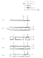
(実施の形態1)
図1(a)〜(e)は本発明の第1の実施の形態における回路基板の製造方法の一部工程断面図であり、図2は同実施の形態における回路基板の製造方法のマスクフィルム貼り付け概略斜視図である。
(Embodiment 1)
1A to 1E are partial process cross-sectional views of a circuit board manufacturing method according to the first embodiment of the present invention, and FIG. 2 is a mask film of the circuit board manufacturing method according to the first embodiment. It is an affixing schematic perspective view.
また、図3は、同実施の形態における回路基板の製造方法のマスクフィルム貼り付け後の一部断面図、図4は同実施の形態における回路基板の製造方法の貫通孔加工後の平面図、図5は同実施の形態における回路基板の製造方法における回路基板を用いたペースト充填時の一部断面図である。 3 is a partial cross-sectional view after attaching a mask film of the circuit board manufacturing method according to the embodiment, and FIG. 4 is a plan view after through-hole processing of the circuit board manufacturing method according to the embodiment. FIG. 5 is a partial cross-sectional view at the time of paste filling using the circuit board in the circuit board manufacturing method according to the embodiment.
図1〜図5において、1は300mm×500mm、厚さ約150μmのプリプレグシートであり、不織布の全芳香族ポリアミド繊維に熱硬化性エポキシ樹脂を含浸させた複合材からなる基材を用いている。2a,2bはマスクフィルムであり、厚さ約20μm、幅300mmのポリエチレンテレフタレートを用いている。
1 to 5,
3は貫通孔であり、4は電気的に接続する導電性ペーストである。 3 is a through hole, and 4 is a conductive paste for electrical connection.
本発明の回路基板の製造は、まずプリプレグシート1に貼り付ける前の段階で、前もって所定位置にレーザにて加工した直径約150μmの千鳥状の貫通孔からなるスキージクリーニング部6を形成したペースト充填側のマスクフィルム2a(図1(a))と未加工のマスクフィルム2bを用意する。
In the production of the circuit board of the present invention, first, before being attached to the
ここではレーザを用いて千鳥状の貫通孔でスキージクリーニング部6を形成したが、非貫通孔でもよく、直線状の溝でもよい。
Here, the
また、安価でかつメンテ性が安易な切削刃を用いて非貫通の直線状の加工溝としてもよい。 Moreover, it is good also as a non-penetrating linear process groove | channel using the cutting blade which is cheap and easy to maintain.
形状的には非貫通でも貫通でも構わず、いかなる形状においても加工部周辺のマスクフィルム2aが隆起部7を有することが良く、隆起部7の高さは3μm以上が望ましい。
The shape may be non-penetrating or penetrating, and the mask film 2a around the processed portion may have the raised
3μm以下であると、スキージエッジに付着したペーストを除去する効果が低下する。 If it is 3 μm or less, the effect of removing the paste adhering to the squeegee edge is lowered.
また、千鳥状でスキージクリーニング部6を形成する場合は、形成した孔が図6に示すように、各々の孔が面一あるいは重なり合うピッチで配置するのが好ましく、これによりスキージ全体に付着したペーストを残らず除去できるというものである。
Further, when forming the
次に図1(b)および図2に示すように、プリプレグシート1とマスクフィルム2a,2bの張り合わせはラミネート装置を用いて加熱したラミネートロール8で加熱加圧してプリプレグシート1の樹脂成分を溶融させてマスクフィルム2a,2bが連続的に接着する。
Next, as shown in FIGS. 1B and 2, the
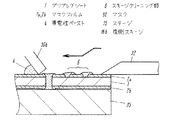
図3にマスクフィルム2a,2b貼り付け後の断面図を示すように、隆起部7を有した貫通孔でスキージクリーニング部6を形成したマスクフィルム2a面を導電性ペースト4充填側に、未加工のマスクフィルム2bを裏面側にして貼り付けている。
As shown in the sectional view after the
次に図1(c)に示すように、上記プリプレグシート1を位置決めして製品の表裏を電気接続するための直径約150μmの貫通孔3を炭酸ガスなどのレーザを用いて加工する。図4に貫通孔3形成後のプリプレグシート1の平面図を示すが、製品エリア16内に製品に必要な貫通孔3を形成し、スキージクリーニング部6は製品エリア16外で、かつペースト充填エリア15内に位置している。
Next, as shown in FIG. 1C, the through-
次に図1(d)および図5に示すように、ペースト充填機の往側スキージ36aの導電性ペースト4充填開始側がプリプレグシート1の上のスキージクリーニング部6となるようにペースト充填機のステージ35に位置決めしてセットし、貫通孔3に導電性ペースト4を充填する。
Next, as shown in FIGS. 1D and 5, the stage of the paste filling machine is such that the conductive paste 4 filling start side of the forward squeegee 36 a of the paste filling machine becomes the
充填方法は従来例と同一であるため詳細な説明を省略するが、本発明の実施の形態1の回路基板の製造法では、図5に示すように、往側スキージ36aで導電性ペースト4の充填をスタートすると、まずスキージクリーニング部6に往側スキージ36aが接触し、スキージエッジに形成された堅い導電性ペースト4が除去されスキージクリーニング部6にペースト残りが発生するが、スキージエッジがクリーニングされているため、その後の製品内の貫通孔3上には導電性ペースト4の残りはなく、安定して充填されていることを確認した。
Since the filling method is the same as that of the conventional example, the detailed description is omitted. However, in the method of manufacturing the circuit board according to the first embodiment of the present invention, as shown in FIG. When filling is started, the forward squeegee 36a first comes into contact with the
また、スキージクリーニング部6はマスクフィルム2bのみ貫通しているため、導電性ペースト4はマスクフィルム2b内にのみ充填されている。
Moreover, since the
そして図1(e)に示すように、プリプレグシート1の両面からマスクフィルム2a,2bを剥離する。剥離時に接続品質に影響のないスキージクリーニング部6の導電性ペースト4はマスクフィルム2a側に取られ不安定な厚みとなって残るが、製品内の貫通孔3はマスクフィルム2aに取られることはなく、安定したペースト充填量が確保できた。
And as shown in FIG.1 (e),
以降の工程は従来例と同一であるため図示しないが、その後プリプレグシート1の両面に銅などの金属を重ね、この状態で熱プレスで加熱加圧することにより、プリプレグシート1の厚みを圧縮するとともにプリプレグシート1と金属箔と接着し、両面の金属は所定位置に設けた貫通孔3に充填された導電性ペースト4により電気的に接続している。
Since the subsequent steps are the same as the conventional example, they are not shown in the drawing. Thereafter, a metal such as copper is superimposed on both surfaces of the
そして、貫通孔3に導電性ペースト4が充填されたプリプレグシート1を100枚確認したが、スキージクリーニング部6通過後、製品内の貫通孔3上にペースト残りはなく、マスクフィルム2a,2b剥離時もマスクフィルム2a,2bに導電性ペースト4が取られて品質に影響を及ぼすことがないことを確認した。
Then, 100
また、スキージクリーニング部6を千鳥状でかつ各々の貫通孔を重ならないように隙間をあけて形成すると、重ねて形成した時と同様に全ての貫通孔上に除去された導電性ペースト4が残っているのが確認されたが貫通孔間の隙間の部分は除去されず、製品内の貫通孔3上に残る場合があることを確認した。
Further, when the
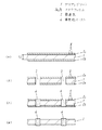
(実施の形態2)
図6(a)〜(d)はそれぞれ本発明の第2の実施の形態における回路基板の製造方法の一部工程断面図、図7は同実施の形態における回路基板の製造方法および製造装置のマスクフィルム貼り付けとスキージクリーニング部形成の概略斜視図である。
(Embodiment 2)
6 (a) to 6 (d) are partial process cross-sectional views of the circuit board manufacturing method according to the second embodiment of the present invention. FIG. 7 is a circuit board manufacturing method and manufacturing apparatus according to the same embodiment. It is a schematic perspective view of mask film sticking and squeegee cleaning part formation.
また、図8は同実施の形態における回路基板の製造方法および製造装置のスキージクリーニング部形成のための溝加工部の概略構成斜視図、図9は同実施の形態における回路基板の製造方法のマスクフィルム貼り付けおよびスキージクリーニング部6形成後の一部断面図である。
FIG. 8 is a schematic perspective view of the groove processing portion for forming the squeegee cleaning portion of the circuit board manufacturing method and manufacturing apparatus according to the embodiment, and FIG. 9 is a mask of the circuit board manufacturing method according to the embodiment. It is a partial cross-sectional view after film pasting and
図6〜図9において、1は300mm×500mm、厚さ約150μmのプリプレグシートであり、不織布の全芳香族ポリアミド繊維に熱硬化性エポキシ樹脂を含浸させた複合材からなる基材を用いている。2a,2bはマスクフィルムであり、厚さ約20μm、幅300mmのポリエチレンテレフタレートを用いている。
6 to 9,
3は貫通孔であり、プリプレグシート1の両面に貼り付ける厚さ35μmの銅などの金属箔25a,25bであり、4は電気的に接続する導電性ペーストである。
本発明の回路基板の製造は、まず図6(a)および図7に示すように、プリプレグシート1とマスクフィルム2a,2bの張り合わせはラミネート装置を用いて加熱したラミネートロール8で加熱加圧して、プリプレグシート1の樹脂成分を溶融させてマスクフィルム2a,2bを約2m/minの速度で連続的に接着する。
In the manufacture of the circuit board of the present invention, as shown in FIGS. 6A and 7, first, the
そして、ラミネートロール8でプリプレグシート1にマスクフィルム2a,2bを貼り付けた後、溝加工部9で連続的にマスクフィルム2aを非貫通状態で切削して1本の直線状の溝加工を行ってスキージクリーニング部6を形成する。
Then, after the
また、溝加工時の丸刃13の受けロール17はプリプレグシート1への傷防止として回転させているが、傷が付かない平滑面であれば回転を止めても平板状であってもよい。
Further, the receiving roll 17 of the round blade 13 at the time of grooving is rotated to prevent scratches on the
ここでは、1本の溝加工としたが、複数本とすることでスキージクリーニング部6形成時やペースト充填時のプリプレグシート1との位置決めばらつきの影響を吸収するとともに、スキージクリーニング効果をより確実なものにできる。
Here, one groove is processed, but by using a plurality of grooves, the influence of the positioning variation with the
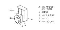
溝加工部9は図8に示すように、直径20mm、板厚300μm、刃先角度60度の超鋼からなる丸刃13と丸刃13を固定する加工刃固定ネジ14と加工刃固定部12、および摺動部11を配置した加工刃固定部取り付け部10からなり、丸刃13は回転しないように加工刃固定ネジ14で加工刃固定部12に取り付けてあり、加工刃固定部12は加工刃固定部取り付け部10の摺動部11で上下方向に摺動する構造となっている。
As shown in FIG. 8, the groove machining portion 9 includes a round blade 13 made of super steel having a diameter of 20 mm, a plate thickness of 300 μm, and a blade edge angle of 60 degrees, a machining
また、図8に示すように、丸刃13の受けロール17はプリプレグシート1への傷防止として回転させているが、傷が付かない平滑面であれば回転を止めても平板状であってもよい。
Further, as shown in FIG. 8, the receiving roll 17 of the round blade 13 is rotated to prevent scratches on the
加工刃13の荷重が約140gとなるよう、可動部の総重量を調整して加工した結果、加工したスキージクリーニング部6は図9に示すように、深さ約10μmで高さ約6μmの隆起部7を有した非貫通の直線状の溝が得られた。
As a result of adjusting and processing the total weight of the movable part so that the load of the processing blade 13 is about 140 g, the processed
また加工溝の深さや隆起部7の高さは、丸刃13の刃先角度によって切削時のマスクフィルム2aの押し広げ量や丸刃13への荷重で溝深さを調整することで制御できる。
Further, the depth of the processed groove and the height of the raised
発明者の実験によれば刃先角度は30〜90度が好ましく、丸刃13への荷重は導電性ペースト4充填後のマスクフィルム2a,2b剥離時に破断しない荷重でかつ隆起部7が3μm以上となるように設定すればよい。
According to the inventor's experiments, the blade edge angle is preferably 30 to 90 degrees, and the load on the round blade 13 is a load that does not break when the
また、スキージクリーニング部6の形成はプリプレグシート1の所定位置に形成するため、あらかじめマスクフィルム2aに加工しておく本発明の実施の形態1では、マスクフィルム2aを交換する毎にプリプレグシート1とを精度よく位置決めする必要があるが、本発明の回路基板の製造方法では、一度プリプレグシート1と溝加工部9の位置決めすれば良く、マスクフィルム2a交換毎の高精度の位置決めは不要となる。
In addition, since the
なお、本実施の形態では丸刃13を用いてスキージクリーニング部6を形成したが、レーザを用いて非貫通の溝加工や千鳥状の円形加工および千鳥状の貫通孔を形成してスキージクリーニング部6としてもよい。
In this embodiment, the
また、千鳥状でスキージクリーニング部6を形成する場合は、実施の形態1と同様に、スキージ全体に付着したペーストを残らず除去するために各々の孔が面一あるいは重なり合うピッチで配置するのが好ましい。
Further, when the
次に、図6(b)に示すように、上記プリプレグシート1を位置決めして実施の形態1と同様に製品の表裏を電気接続するための貫通孔3を炭酸ガスなどのレーザを用いて加工する。
Next, as shown in FIG. 6 (b), the
次に図6(c)に示すように、ペースト充填機を用いて実施の形態1と同様で貫通孔3に導電性ペースト4を充填する。
Next, as shown in FIG. 6 (c), the conductive paste 4 is filled into the through
プリプレグシート1のセッティングは実施の形態1と充填方法は従来例とそれぞれ同一であるため詳細な説明を省略するが、本発明の実施の形態2の回路基板の製造法では、実施の形態1同様に、スキージエッジに形成された堅い導電性ペースト4が除去されスキージクリーニング部6にペースト残りが発生するが、スキージエッジがクリーニングされているため、その後の製品内の貫通孔3上には導電性ペースト4の残りはなく、安定して充填されていることを確認した。
Since the setting of the
また、スキージクリーニング部6はマスクフィルム2bを非貫通の溝加工で形成しているため、導電性ペースト4はマスクフィルム2b内の溝深さ位置まで充填されている。
Further, since the
そして図6(d)に示すように、プリプレグシート1の両面からマスクフィルム2a,2bを剥離する。本発明のスキージクリーニング部6はマスクフィルム2aに非貫通の溝加工で形成しているため、導電性ペースト4はプリプレグシート1面には到達しておらず、剥離時にプリプレグシート1上に不要なペーストが残らず、かつ製品内の貫通孔3はマスクフィルム2aに取られることはなく、安定したペースト充填量が確保できた。
Then, as shown in FIG. 6 (d), the
以降の工程は従来例と同一であるため図示しないが、その後プリプレグシート1の両面に銅などの金属を重ね、この状態で熱プレスで加熱加圧することにより、プリプレグシート1の厚みを圧縮するとともにプリプレグシート1と金属箔と接着し、両面の金属は所定位置に設けた貫通孔3に充填された導電性ペースト4により電気的に接続している。
Since the subsequent steps are the same as the conventional example, it is not shown in the figure, but after that, a metal such as copper is superimposed on both surfaces of the
そして、貫通孔3に導電性ペースト4が充填されたプリプレグシート1を100枚確認したが、本発明の実施の形態1と同様にスキージクリーニング部6通過後、製品内の貫通孔3上にペースト残りはなく、マスクフィルム2a,2b剥離時もマスクフィルム2a,2bに導電性ペースト4が取られて品質に影響を及ぼすことがないことを確認した。
And 100 sheets of the
本発明の実施の形態1および2ではスキージクリーニング部6は、少なくとも最後のスキージの動作開始側プリプレグシート1の一辺に設ければよいが、他方の辺にも設けてもよい。
In
また、本発明の実施の形態1および2では基板材料をアラミド繊維を主体とした不織布に熱硬化性樹脂を主体とする樹脂材料を含浸しBステージ化したものを用いたが、繊維にアラミド織布や、ガラス繊維の織布や不織布を用いても同様の効果が得られることは言うまでもない。 In the first and second embodiments of the present invention, a non-woven fabric mainly composed of aramid fibers is impregnated with a resin material mainly composed of a thermosetting resin to form a B-stage. Needless to say, the same effect can be obtained by using a cloth or a glass fiber woven or non-woven fabric.
アラミド繊維、ガラス繊維を主体とした樹脂材料は、耐熱性や機械的、物理的特性に優れ、特にアラミド繊維は軽量化において有利である。 Resin materials mainly composed of aramid fibers and glass fibers are excellent in heat resistance, mechanical properties, and physical properties. In particular, aramid fibers are advantageous in terms of weight reduction.
また、Bステージ化状態のプリプレグ材料を用いることによって、レーザ加工による貫通孔3の微細化が可能となり、導電性ペースト4を充填することによって導通孔を形成することが可能となる。特に、本発明の手段を用いることによって、安定した導通接続を図ることができる。
Further, by using the B-staged prepreg material, the through
本発明にかかる回路基板の製造法と回路基板への印刷方法は、両面あるいは多層配線基板の層間を導電性ペーストで電気的接続する際の貫通孔への導電性ペースト充填時の不具合を解消して接続品質の安定化が図れるもので、マスクフィルムを用いた貫通孔や非貫通孔への導電性ペースト充填が必要な回路基板全般に有用である。 The method of manufacturing a circuit board and the method of printing on the circuit board according to the present invention eliminates the problem of filling the through hole with the conductive paste when electrically connecting the layers of both sides or the multilayer wiring board with the conductive paste. Thus, the connection quality can be stabilized, and it is useful for all circuit boards that need to be filled with conductive paste in through holes and non-through holes using a mask film.
1,21 プリプレグシート
2a,2b,22a,22b マスクフィルム
3,23 貫通孔
4,24 導電性ペースト
6 スキージクリーニング部
7 隆起部
8 ラミネートロール
9 溝加工部
10 加工刃固定部取り付け部
11 摺動部
12 加工刃固定部
13 加工刃
14 加工刃固定ネジ
15 ペースト充填エリア
16 製品エリア
25a,25b 金属箔
30 版
31 版枠
32 マスク
33 開口部
34 傾斜部
35 ステージ
36a 往側スキージ
36b 復側スキージ
1,21
Claims (20)
前記溝加工部は、特定の刃先角度を有する加工刃を備えた加工刃固定部と、摺動部を配置した加工刃固定部取り付け部からなり、加工刃固定部は加工刃固定部取り付け部の摺動部で上下方向に摺動可能であり、
前記加工刃は加工刃固定ネジで前記加工刃固定部に取り付けられるものであり、
前記加工刃固定部の総重量は調整可能であることを特徴とする回路基板の製造装置。 A conveying means for conveying the substrate material, a mask film supply means positioned above and below the conveying means, and a laminating roll, and a mask film groove processing portion at the rear of the laminating roll and above the conveying means,
The groove processing portion includes a processing blade fixing portion having a processing blade having a specific cutting edge angle, and a processing blade fixing portion mounting portion having a sliding portion, and the processing blade fixing portion is a portion of the processing blade fixing portion mounting portion. It can slide up and down at the sliding part,
The processing blade is attached to the processing blade fixing portion with a processing blade fixing screw,
An apparatus for manufacturing a circuit board, wherein the total weight of the processing blade fixing portion is adjustable.
Priority Applications (7)
| Application Number | Priority Date | Filing Date | Title |
|---|---|---|---|
| JP2003433147A JP3972902B2 (en) | 2003-12-26 | 2003-12-26 | Circuit board manufacturing method and manufacturing apparatus |
| PCT/JP2004/018693 WO2005065001A1 (en) | 2003-12-26 | 2004-12-15 | Method and apparatus for manufacturing circuit board |
| US10/540,606 US8211494B2 (en) | 2003-12-26 | 2004-12-15 | Method and apparatus for manufacturing circuit board |
| CNB2004800021657A CN100482045C (en) | 2003-12-26 | 2004-12-15 | Method and apparatus for manufacturing circuit board |
| KR1020057013177A KR100655731B1 (en) | 2003-12-26 | 2004-12-15 | Method and apparatus for manufacturing circuit board |
| EP04807052A EP1587351A4 (en) | 2003-12-26 | 2004-12-15 | Method and apparatus for manufacturing circuit board |
| TW093139192A TW200526101A (en) | 2003-12-26 | 2004-12-16 | Method and apparatus for manufacturing circuit board |
Applications Claiming Priority (1)
| Application Number | Priority Date | Filing Date | Title |
|---|---|---|---|
| JP2003433147A JP3972902B2 (en) | 2003-12-26 | 2003-12-26 | Circuit board manufacturing method and manufacturing apparatus |
Publications (2)
| Publication Number | Publication Date |
|---|---|
| JP2005191410A JP2005191410A (en) | 2005-07-14 |
| JP3972902B2 true JP3972902B2 (en) | 2007-09-05 |
Family
ID=34736504
Family Applications (1)
| Application Number | Title | Priority Date | Filing Date |
|---|---|---|---|
| JP2003433147A Expired - Fee Related JP3972902B2 (en) | 2003-12-26 | 2003-12-26 | Circuit board manufacturing method and manufacturing apparatus |
Country Status (7)
| Country | Link |
|---|---|
| US (1) | US8211494B2 (en) |
| EP (1) | EP1587351A4 (en) |
| JP (1) | JP3972902B2 (en) |
| KR (1) | KR100655731B1 (en) |
| CN (1) | CN100482045C (en) |
| TW (1) | TW200526101A (en) |
| WO (1) | WO2005065001A1 (en) |
Families Citing this family (8)
| Publication number | Priority date | Publication date | Assignee | Title |
|---|---|---|---|---|
| DE102005011545A1 (en) * | 2005-03-10 | 2006-09-21 | Lpkf Laser & Electronics Ag | Method for contacting printed conductors of a printed circuit board |
| JP2011049664A (en) * | 2009-08-25 | 2011-03-10 | Seiko Instruments Inc | Method for manufacturing package, method for manufacturing piezoelectric vibrator, oscillator, electronic device, and radio-controlled timepiece |
| NL2003627C2 (en) * | 2009-10-12 | 2011-04-13 | Stork Prints Bv | Screen printing. |
| CN103517558B (en) * | 2012-06-20 | 2017-03-22 | 碁鼎科技秦皇岛有限公司 | Manufacture method for package substrate |
| KR101527941B1 (en) * | 2015-03-17 | 2015-06-11 | 김창열 | The Repairing Method of Multilayer Test Board for Semiconductor Device |
| CN107264008B (en) * | 2017-07-05 | 2019-07-16 | 京东方科技集团股份有限公司 | A kind of printing process of printing mask plate and glue pattern |
| KR20230002297A (en) * | 2020-04-23 | 2023-01-05 | 엘지이노텍 주식회사 | Metal deposition mask for OLED pixel deposition and manufacturing method of deposition mask |
| CN111629519B (en) * | 2020-05-18 | 2021-04-09 | 微智医疗器械有限公司 | Chip and circuit board connecting method, circuit board assembly and electronic equipment |
Family Cites Families (15)
| Publication number | Priority date | Publication date | Assignee | Title |
|---|---|---|---|---|
| JPS57103862A (en) * | 1980-12-19 | 1982-06-28 | Fuji Xerox Co Ltd | Heat sensitive recording head |
| JPS57103862U (en) * | 1980-12-19 | 1982-06-26 | ||
| JP2629067B2 (en) | 1990-10-11 | 1997-07-09 | 東洋インキ製造株式会社 | Monoazo lake pigment and printing ink composition |
| JPH05177811A (en) * | 1992-01-06 | 1993-07-20 | Furukawa Electric Co Ltd:The | Cleaning method and its device of printing mask |
| JP2601128B2 (en) | 1992-05-06 | 1997-04-16 | 松下電器産業株式会社 | Method of manufacturing circuit forming substrate and circuit forming substrate |
| JPH05338370A (en) * | 1992-06-10 | 1993-12-21 | Dainippon Screen Mfg Co Ltd | Metal mask plate for screen printing |
| JP2768236B2 (en) | 1993-10-08 | 1998-06-25 | 松下電器産業株式会社 | Method for manufacturing multilayer substrate |
| DE69737281T2 (en) * | 1996-12-10 | 2007-12-20 | Matsushita Electric Industrial Co., Ltd., Kadoma | Apparatus and method for printing solder paste |
| JP3533596B2 (en) * | 1999-06-25 | 2004-05-31 | 日本特殊陶業株式会社 | Manufacturing method of wiring board |
| JP3459380B2 (en) * | 1999-06-30 | 2003-10-20 | 日本特殊陶業株式会社 | Manufacturing method of printed wiring board and mask |
| JP3292194B2 (en) * | 2000-02-01 | 2002-06-17 | 松下電器産業株式会社 | Printing plate and printing method using the same |
| US6638363B2 (en) * | 2000-11-22 | 2003-10-28 | Gunter Erdmann | Method of cleaning solder paste |
| JP3721982B2 (en) * | 2000-12-04 | 2005-11-30 | 松下電器産業株式会社 | Circuit forming substrate manufacturing method and circuit forming substrate manufacturing apparatus |
| JP2003033967A (en) * | 2001-07-23 | 2003-02-04 | Pearl Kogyo Kk | Method and device for working resin material |
| CN1318228C (en) * | 2002-09-24 | 2007-05-30 | 松下电器产业株式会社 | Printing plate, circuit board and method of printing circuit board |
-
2003
- 2003-12-26 JP JP2003433147A patent/JP3972902B2/en not_active Expired - Fee Related
-
2004
- 2004-12-15 CN CNB2004800021657A patent/CN100482045C/en not_active Expired - Fee Related
- 2004-12-15 EP EP04807052A patent/EP1587351A4/en not_active Withdrawn
- 2004-12-15 WO PCT/JP2004/018693 patent/WO2005065001A1/en active IP Right Grant
- 2004-12-15 KR KR1020057013177A patent/KR100655731B1/en not_active IP Right Cessation
- 2004-12-15 US US10/540,606 patent/US8211494B2/en not_active Expired - Fee Related
- 2004-12-16 TW TW093139192A patent/TW200526101A/en not_active IP Right Cessation
Also Published As
| Publication number | Publication date |
|---|---|
| JP2005191410A (en) | 2005-07-14 |
| TW200526101A (en) | 2005-08-01 |
| EP1587351A4 (en) | 2009-04-01 |
| US20060115583A1 (en) | 2006-06-01 |
| KR100655731B1 (en) | 2006-12-11 |
| TWI335196B (en) | 2010-12-21 |
| KR20060006998A (en) | 2006-01-23 |
| CN1739322A (en) | 2006-02-22 |
| US8211494B2 (en) | 2012-07-03 |
| WO2005065001A1 (en) | 2005-07-14 |
| CN100482045C (en) | 2009-04-22 |
| EP1587351A1 (en) | 2005-10-19 |
Similar Documents
| Publication | Publication Date | Title |
|---|---|---|
| EP1167029B1 (en) | Printing plate, and printing method using the same | |
| JP3972902B2 (en) | Circuit board manufacturing method and manufacturing apparatus | |
| WO2004095900A1 (en) | Multilayer printed wiring board-use copper-clad laminate sheet, multilayer printed wiring board and production method for multilayer printed wiring board | |
| EP0032932A1 (en) | Backup material and method for drilling | |
| KR100748208B1 (en) | A laminating device of flexible printed circuits board and the making methed thereof | |
| JP2768236B2 (en) | Method for manufacturing multilayer substrate | |
| KR20060037238A (en) | Method of manufacturing circuit board | |
| JP2011031507A (en) | Printing plate | |
| JP3654279B2 (en) | Circuit board and method for printing on circuit board | |
| JP3922146B2 (en) | Printing plate and printing method using the same | |
| US7105277B2 (en) | Printing plate, circuit board and method of printing circuit board | |
| JP3732905B2 (en) | Circuit board manufacturing equipment | |
| JP4590939B2 (en) | Insulating resin film for printed wiring board and method of forming insulating layer using the same | |
| JP4170781B2 (en) | Substrate manufacturing method | |
| JP2001160684A (en) | Apparatus and method for manufacturing multilayer wiring board | |
| JP4395741B2 (en) | Multilayer substrate manufacturing method | |
| JP5124977B2 (en) | Paste filling method | |
| JP5011784B2 (en) | Printing plate and printing method using the same | |
| JP2011035372A (en) | Method of manufacturing substrate sheet with conductive bump, and method of manufacturing multilayer printed wiring board | |
| JP2000151116A (en) | Method and device for manufacturing multilayer printed board | |
| JP2005123320A (en) | Method and device for manufacturing multilayer printed wiring board | |
| JPH11238958A (en) | Manufacture and manufacturing device of circuit board | |
| JP2009234223A (en) | Copper-clad laminated sheet, method for manufacturing wiring substrate using this, method for processing end face of copper-clad laminated sheet and end face processing apparatus used for this | |
| JP2004253405A (en) | Method of manufacturing film-embedded board | |
| WO2024033720A1 (en) | Methods to fill through-holes of a substrate with metal paste |
Legal Events
| Date | Code | Title | Description |
|---|---|---|---|
| RD01 | Notification of change of attorney |
Free format text: JAPANESE INTERMEDIATE CODE: A7421 Effective date: 20050708 |
|
| A131 | Notification of reasons for refusal |
Free format text: JAPANESE INTERMEDIATE CODE: A131 Effective date: 20070306 |
|
| A521 | Request for written amendment filed |
Free format text: JAPANESE INTERMEDIATE CODE: A523 Effective date: 20070424 |
|
| TRDD | Decision of grant or rejection written | ||
| A01 | Written decision to grant a patent or to grant a registration (utility model) |
Free format text: JAPANESE INTERMEDIATE CODE: A01 Effective date: 20070522 |
|
| A61 | First payment of annual fees (during grant procedure) |
Free format text: JAPANESE INTERMEDIATE CODE: A61 Effective date: 20070604 |
|
| FPAY | Renewal fee payment (event date is renewal date of database) |
Free format text: PAYMENT UNTIL: 20100622 Year of fee payment: 3 |
|
| FPAY | Renewal fee payment (event date is renewal date of database) |
Free format text: PAYMENT UNTIL: 20100622 Year of fee payment: 3 |
|
| FPAY | Renewal fee payment (event date is renewal date of database) |
Free format text: PAYMENT UNTIL: 20110622 Year of fee payment: 4 |
|
| FPAY | Renewal fee payment (event date is renewal date of database) |
Free format text: PAYMENT UNTIL: 20120622 Year of fee payment: 5 |
|
| FPAY | Renewal fee payment (event date is renewal date of database) |
Free format text: PAYMENT UNTIL: 20120622 Year of fee payment: 5 |
|
| FPAY | Renewal fee payment (event date is renewal date of database) |
Free format text: PAYMENT UNTIL: 20130622 Year of fee payment: 6 |
|
| LAPS | Cancellation because of no payment of annual fees |