JP3630489B2 - Liquid crystal display - Google Patents
Liquid crystal display Download PDFInfo
- Publication number
- JP3630489B2 JP3630489B2 JP4070396A JP4070396A JP3630489B2 JP 3630489 B2 JP3630489 B2 JP 3630489B2 JP 4070396 A JP4070396 A JP 4070396A JP 4070396 A JP4070396 A JP 4070396A JP 3630489 B2 JP3630489 B2 JP 3630489B2
- Authority
- JP
- Japan
- Prior art keywords
- liquid crystal
- crystal display
- display device
- pixel
- circuit
- Prior art date
- Legal status (The legal status is an assumption and is not a legal conclusion. Google has not performed a legal analysis and makes no representation as to the accuracy of the status listed.)
- Expired - Fee Related
Links
Images


Classifications
-
- G—PHYSICS
- G09—EDUCATION; CRYPTOGRAPHY; DISPLAY; ADVERTISING; SEALS
- G09G—ARRANGEMENTS OR CIRCUITS FOR CONTROL OF INDICATING DEVICES USING STATIC MEANS TO PRESENT VARIABLE INFORMATION
- G09G3/00—Control arrangements or circuits, of interest only in connection with visual indicators other than cathode-ray tubes
- G09G3/20—Control arrangements or circuits, of interest only in connection with visual indicators other than cathode-ray tubes for presentation of an assembly of a number of characters, e.g. a page, by composing the assembly by combination of individual elements arranged in a matrix no fixed position being assigned to or needed to be assigned to the individual characters or partial characters
- G09G3/34—Control arrangements or circuits, of interest only in connection with visual indicators other than cathode-ray tubes for presentation of an assembly of a number of characters, e.g. a page, by composing the assembly by combination of individual elements arranged in a matrix no fixed position being assigned to or needed to be assigned to the individual characters or partial characters by control of light from an independent source
- G09G3/36—Control arrangements or circuits, of interest only in connection with visual indicators other than cathode-ray tubes for presentation of an assembly of a number of characters, e.g. a page, by composing the assembly by combination of individual elements arranged in a matrix no fixed position being assigned to or needed to be assigned to the individual characters or partial characters by control of light from an independent source using liquid crystals
- G09G3/3611—Control of matrices with row and column drivers
- G09G3/3685—Details of drivers for data electrodes
- G09G3/3688—Details of drivers for data electrodes suitable for active matrices only
-
- G—PHYSICS
- G06—COMPUTING; CALCULATING OR COUNTING
- G06F—ELECTRIC DIGITAL DATA PROCESSING
- G06F3/00—Input arrangements for transferring data to be processed into a form capable of being handled by the computer; Output arrangements for transferring data from processing unit to output unit, e.g. interface arrangements
- G06F3/01—Input arrangements or combined input and output arrangements for interaction between user and computer
- G06F3/03—Arrangements for converting the position or the displacement of a member into a coded form
- G06F3/033—Pointing devices displaced or positioned by the user, e.g. mice, trackballs, pens or joysticks; Accessories therefor
- G06F3/0354—Pointing devices displaced or positioned by the user, e.g. mice, trackballs, pens or joysticks; Accessories therefor with detection of 2D relative movements between the device, or an operating part thereof, and a plane or surface, e.g. 2D mice, trackballs, pens or pucks
- G06F3/03542—Light pens for emitting or receiving light
-
- G—PHYSICS
- G09—EDUCATION; CRYPTOGRAPHY; DISPLAY; ADVERTISING; SEALS
- G09G—ARRANGEMENTS OR CIRCUITS FOR CONTROL OF INDICATING DEVICES USING STATIC MEANS TO PRESENT VARIABLE INFORMATION
- G09G3/00—Control arrangements or circuits, of interest only in connection with visual indicators other than cathode-ray tubes
- G09G3/20—Control arrangements or circuits, of interest only in connection with visual indicators other than cathode-ray tubes for presentation of an assembly of a number of characters, e.g. a page, by composing the assembly by combination of individual elements arranged in a matrix no fixed position being assigned to or needed to be assigned to the individual characters or partial characters
- G09G3/34—Control arrangements or circuits, of interest only in connection with visual indicators other than cathode-ray tubes for presentation of an assembly of a number of characters, e.g. a page, by composing the assembly by combination of individual elements arranged in a matrix no fixed position being assigned to or needed to be assigned to the individual characters or partial characters by control of light from an independent source
- G09G3/36—Control arrangements or circuits, of interest only in connection with visual indicators other than cathode-ray tubes for presentation of an assembly of a number of characters, e.g. a page, by composing the assembly by combination of individual elements arranged in a matrix no fixed position being assigned to or needed to be assigned to the individual characters or partial characters by control of light from an independent source using liquid crystals
- G09G3/3611—Control of matrices with row and column drivers
- G09G3/3648—Control of matrices with row and column drivers using an active matrix
- G09G3/3659—Control of matrices with row and column drivers using an active matrix the addressing of the pixel involving the control of two or more scan electrodes or two or more data electrodes, e.g. pixel voltage dependant on signal of two data electrodes
-
- G—PHYSICS
- G09—EDUCATION; CRYPTOGRAPHY; DISPLAY; ADVERTISING; SEALS
- G09G—ARRANGEMENTS OR CIRCUITS FOR CONTROL OF INDICATING DEVICES USING STATIC MEANS TO PRESENT VARIABLE INFORMATION
- G09G2300/00—Aspects of the constitution of display devices
- G09G2300/08—Active matrix structure, i.e. with use of active elements, inclusive of non-linear two terminal elements, in the pixels together with light emitting or modulating elements
- G09G2300/0809—Several active elements per pixel in active matrix panels
- G09G2300/0842—Several active elements per pixel in active matrix panels forming a memory circuit, e.g. a dynamic memory with one capacitor
- G09G2300/0857—Static memory circuit, e.g. flip-flop
-
- G—PHYSICS
- G09—EDUCATION; CRYPTOGRAPHY; DISPLAY; ADVERTISING; SEALS
- G09G—ARRANGEMENTS OR CIRCUITS FOR CONTROL OF INDICATING DEVICES USING STATIC MEANS TO PRESENT VARIABLE INFORMATION
- G09G2310/00—Command of the display device
- G09G2310/02—Addressing, scanning or driving the display screen or processing steps related thereto
- G09G2310/0232—Special driving of display border areas
-
- G—PHYSICS
- G09—EDUCATION; CRYPTOGRAPHY; DISPLAY; ADVERTISING; SEALS
- G09G—ARRANGEMENTS OR CIRCUITS FOR CONTROL OF INDICATING DEVICES USING STATIC MEANS TO PRESENT VARIABLE INFORMATION
- G09G2330/00—Aspects of power supply; Aspects of display protection and defect management
- G09G2330/02—Details of power systems and of start or stop of display operation
- G09G2330/021—Power management, e.g. power saving
Description
【0001】
【発明の属する技術分野】
本発明は、液晶表示装置に係り、特に携帯用パソコンなど小型情報端末の表示デバイスとして好適な、高精細画像の表示を低消費電力で実現できる液晶表示装置に関する。
【0002】
【従来の技術】
液晶表示装置は、陰極線管(CRT)に代わるディスプレイデバイスとして、各種情報処理機器の画像表示装置あるいはポータブルテレビや壁掛けテレビなどに広く用いられている。特に近年は薄型・軽量化が可能なディスプレイデバイスとして注目されており、いわゆるノートブック型パソコンのような携帯型の情報処理機器等に用いられている。
【0003】
そのような液晶表示装置の中でも特に多結晶シリコン(以下、p−Siと略称する)で形成された薄膜トランジスタ(以下、TFTと略称)などの薄膜トランジスタ(Thin Film Transistor:以下、TFTと略称)をスイッチング素子として画素部に設ける一方、同様な構造のTFTをスイッチング素子アレイ基板の周縁部にも設けて液晶表示回路を形成した、いわゆる駆動回路一体型のアクティブマトリックス型液晶表示装置の研究・開発が盛んに行なわれている。
【0004】
ここで、従来の液晶表示装置、特にアクティブマトリックス型液晶表示装置の構成とその動作について簡潔に述べる。
【0005】
図19は一般的な従来の液晶表示装置の回路構造の概要を示す図である。
【0006】
従来の液晶表示装置は、マトリックス状に配線された複数のデータ線901および走査線902と、画素電極903と、これら画素電極903とデータ線901との間に、走査線902により制御される画素部スイッチ素子904と、この画素部スイッチ素子904の後段かつ画素電極903の前段に一端が接続され他端はアース接続された電荷蓄積容量905とを備えたスイッチ素子アレイ基板906と、画素電極903に間隙を保持しつつ対向配置される対向電極907を備えた対向基板(図示せず)と、これら対向基板とスイッチ素子アレイ基板との間に周囲を封止されて挾持され前記の各画素電極903と対向電極907との間で液晶容量908を形成する液晶層と、前記のデータ線901を駆動するデータ線ドライバ909および走査線902を駆動する走査線ドライバ910とから、その主要部が構成されている。
【0007】
一般に液晶駆動回路系としては、例えば外付けされたシフトレジスタ型などの液晶ドライバICが用いられる。あるいは、例えばp−SiTFTを前記の画素部スイッチ素子904として用いてこのp−SiTFTで上記の液晶駆動回路系をも同一基板上に直接形成する、いわゆる液晶駆動回路一体型の液晶表示装置も提案されている。
【0008】
次に、上述のような従来の構造の液晶表示装置の動作について簡潔に述べる。走査線ドライバ回路910により、ある走査線902が選択されると、その走査線902上に接続されている画素部スイッチ素子904が導通状態となる。
【0009】
このとき、データ線ドライバ回路909により画像データに対応したデータ線901が選択されて、そのデータ線901にビデオ信号などの画像データに対応した電圧が印加される。
【0010】
そして前記の選択された走査線902および選択状態となっているデータ線901とに接続されている画素部スイッチ素子904を介して、データ線901から電圧が供給されて電荷蓄積容量905に電荷が蓄積されるとともに、その電圧がそれに接続された画素電極903に書き込まれる。すると液晶セル(液晶容量908)はこの電圧が印加されてその電位に対応した光変調を行なうことによって、画像表示が実現される。
【0011】
1水平走査期間中に、データ線901はデータ線ドライバ909によって左右いずれか一方の端から他端へと順に選択される。そして走査線902側では、ある走査線1列に対してビデオ信号の書き込みが終わると次の走査線902が選択される。このような走査が上から下またはその逆で点順次に行なわれて行き、この走査選択が終端の走査線にまで達すると、再び最初の走査ラインに戻って上記の動作が繰り返される。このような点順次走査を繰り返して、液晶表示装置の画面全体の画像が選択され表示されて行き、各水平走査期間ごとの画面1フレーム(又は1フィールド)が形成される。
【0012】
上記のような液晶表示装置の最大の利点は一般に、前述した如く薄型・軽量という点である。この利点を生かして液晶表示装置は、ノートブック型パソコンのような携帯型情報処理装置のディスプレイデバイスとして搭載されるようになってきた。
【0013】
ノートブック型パソコンなどの携帯型情報処理装置は、携帯可能でなければならないので、一般にバッテリー駆動方式が採用されており、従って、現状では一回の充電で続行可能な使用時間はバッテリーの電力容量に依存して限界がある。
【0014】
そこで、一回の充電で続行可能な使用時間を、より長くするための方策が種々試みられているが、バッテリー自体の電力容量の増大を図ることは言うまでもなく、その一方で液晶表示装置の低消費電力化が重要な課題となっている。
【0015】
特に近年ではバッテリー自体の電力容量については、携帯可能であることが必須条件となっているので、バッテリーの重量を増やすこと無くその電力容量を増大しなければならない。しかしバッテリーの電力容量密度(容量/重量)の向上は、一般的に用いられるバッテリーの分野においてはすでに技術的な向上の限界に近付いており、これ以上の大幅な向上は実際上ほとんど望めないのが現状である。従ってもう一方の、液晶表示装置の低消費電力化が、さらに重要な課題となっている。
【0016】
液晶表示装置の低消費電力化を図るためには、主として2つの方策が考えられる。第1は、液晶表示装置が非発光素子であることにより照明光が必要となるが、この照明光を供給するための電力の低減化である。
【0017】
しかしながら、従来のいわゆるバックライトを用いた液晶表示装置においてはそのバックライトの発光効率および利用効率の向上も、ほとんど限界に近付いているのが現状である。しかも、TFTを用いたアクティブマトリックス型液晶表示装置におけるさらなる画面の高精細化および多画素化につれて、さらに画素部開口率が低下する傾向にあるため、バックライトの点での低消費電力化は困難であるという問題がある。
【0018】
液晶表示装置の低消費電力化を図る第2の方策としては、液晶表示装置自体を駆動してその液晶パネルに画像を表示するために必要な、いわゆる駆動電力の低減化が考えられる。
【0019】
しかし、従来の液晶表示装置では、そのような駆動電力量を大幅に低減することは非常に困難である。
【0020】
従来の液晶表示装置においては一般にダイナミック駆動型と呼べるような駆動方式が採用されている。即ち、従来の液晶表示装置は、図19で示したように、データ線901の電位を一旦、電荷蓄積容量905に蓄えつつ画素電極903にも印加することで、各画素ごとの液晶セル908への液晶印加電圧の書き込みを行なっている。
【0021】
このため、一つの選択期間の次にデータ線901の電位が一つの画素の液晶セルに書き込まれるまでの期間中に、その画素の液晶容量908および電荷蓄積容量905から電流がリークするなどして、液晶容量908の保持している電位が低下し、明度やコントラストの低下等の表示状態の劣化を引き起こす。
【0022】
このため、表示画像を高品位に保つには、静止画像表示の際にも常にデータ線ドライバ909および走査線ドライバ910を動かして、常に各画素に電圧の書き込みを行なってその電位を保持しなければならず、液晶容量および電荷蓄積容量と画素部スイッチ素子とを含めた回路構造に対し、あたかもDRAM(ダイナミックRAM)のように常にリフレッシュを行なわなければならず、液晶駆動回路系を常に動かすための電力および各画素部のリフレッシュを行うための電力を必要とするため、消費電力の点で極めて不利であり、低消費電力化にとってはむしろ逆行するものでさえあるという問題があった。
【0023】
そのような問題の解決を意図した低消費電力型の液晶表示装置として、画素内にメモリ素子を配設されたスタティック型の液晶表示装置が提案されている。
【0024】
画素内にデジタルメモリを有するスタティック型の液晶表示装置は一般に、
(1)静止画像表示時に外部からの映像信号の入力を止めることができ、低消費電力化が図れる。
(2)画素電圧をデジタル化することにより、クロストーク等による表示品質の劣化が起きにくい。
といった利点を備えている。
【0025】
しかしながらその一方で、各画素ごとに複数個の薄膜トランジスタ(TFT)からなるスイッチ素子を組み合わせてなるデジタルメモリが形成されている構造であるため、1画素あたり1個のTFTを画素部スイッチ素子として用いたダイナミック型の液晶表示装置と比較して構造が極めて煩雑であり、またその製造歩留りが低下するという問題がある。
【0026】
そして、近年ますます多画素化、高精細化が進む携帯型情報処理装置に用いられる液晶表示装置にあっては、画素のさらなる微細化が進むため上記のような画素部の構造の煩雑化およびその製造プロセスの煩雑化は著しく進み、その結果、場合によっては前記のデジタルメモリを含んだ回路構造が一画素領域内ごとには収まらなくなる、という問題もある。つまり上記のような構造が実際的には採用不可能となるという問題がある。あるいは、そのような繁雑で大きな占有面積を必要とする回路構造に占有されて残った僅かな面積にしか画素開口部を設けられなくなるので、画面の輝度が低くなる、あるいは狭い画素開口面積で所定の輝度を得るために、バックライトなど照明に要する電力を増加させなければならなくなり、低消費電力化にとってむしろ逆行することになるという問題がある。
【0027】
このような画素内にメモリ素子を備えたスタティック型の液晶表示装置としては、例えば特開昭58−23091号公報などに開示され提案されている。
【0028】
このような従来のスタティック型の液晶表示装置の回路構造の第1の例を図20に、また第2の例を図21に示す。
【0029】
これら従来例は、データ線901に接続しているとともに走査線902によって制御される画素部スイッチ素子904と、メモリ素子911と、各画素の液晶セル(液晶容量908)を交流駆動するために印加電圧を所定のタイミングで極性反転させる付加回路912とを備えて形成されている。
【0030】
これらの基本的な動作は、メモリ素子911にデータ線901からのビデオ信号をラッチし、その信号を各画素の液晶セル(液晶容量908)に書き込む、というものである。
【0031】
ここで、メモリ素子911は、新たな信号が書き込みされるまで前の信号を保持するので、一旦、信号の書き込みを行なってしまえば、前記のデータ線ドライバ909および走査線ドライバ910を停止しても、それまでに書き込まれた画像を静止画像として継続表示することが可能である。従って、静止画像表示の際の液晶表示装置としての駆動の低消費電力化を実現することが可能となる。
【0032】
なお付加回路912としては、第1の従来例ではエクスクルーシブNOR回路を用いた例が、また第2の従来例ではトランスファゲートを用いて各画素ごとに選択的に外部からの交流信号を入力させる例が、それぞれ示されている。
【0033】
ところで、前述したように、液晶セルは直流電圧が印加され続けるとその液晶分子に誘電分極が発生して特性が劣化するため、一般に交流的に駆動されるが、上記の2つの従来例では2相のクロック信号を対向電極と画素電極との両方に印加することで液晶セルを交流駆動している。
【0034】
【発明が解決しようとする課題】
しかしながら、このような従来の液晶表示装置では、対向電極を交流駆動することを前提としてその回路系が形成されているが、対向電極はすべての画素電極に対して液晶層を介して共通に対向して液晶容量を形成するように配置されるものであるため、大きな電気容量成分を持っており、この大容量の電気容量を交流駆動時に充放電するために駆動力(あるいは駆動容量)の大きなドライバ回路系が必要になる。また、そのような大容量の電気容量を充放電するためには、電流をさらに多く消費しなければならなくなる。
【0035】
駆動回路として外付けの液晶ドライバICなどを用いる液晶表示装置の場合には、対向電極側を交流駆動する際に必要な電気容量に対応できる電気容量を備えた液晶ドライバICを選択すれば、従来の技術に係る対向電極側を交流駆動する方式でも採用可能である。しかし、駆動回路系を含めた液晶表示装置全体の小型化および低消費電力化を図るためには、駆動回路系をTFTアレイ基板上に画素部スイッチTFTや画素電極等と一体で形成することが望ましい。このとき、駆動力の大きな液晶ドライバ回路を基板上に薄膜トランジスタ構造で形成すると、その素子面積はその容量に対応して増大するので、液晶ドライバ回路は物理的に大きな面積を占有するという問題がある。しかも、そのような液晶ドライバ回路の製造プロセスもさらに煩雑化し、製造歩留りの低下や信頼性の低下を招くという問題がある。
【0036】
また、前述した従来技術に係る液晶表示装置では、静止画表示時にはスタティック動作により消費電力の大幅な低減を図ることができるが、動きの少ない画像の表示では、画面内に一か所でも動画表示部分があれば、消費電力は通常の動画を表示するダイナミック動作の際の消費電力と同様の消費電力が必要となるという問題がある。
【0037】
さらに、従来例の構造のままでは画素ごとに交流信号の入力が可能ではあっても、単体で入力装置として使用することはできない。従来構造を採用し、これに表示機能に加えて入力機能も持たせようとすると感圧シートやセンサ板などを液晶セルに挟み、あるいは上置きすることが必要となるため、セル厚が増加せざるを得ない。これは携帯機器に搭載するのに不利であるばかりでなく、部材低減の側面から見ても問題である。
【0038】
本発明は、上述のような従来技術の問題点、即ち、
第1に、液晶セルを交流駆動するために要する電力量が液晶表示装置の消費電力量として大き過ぎるという問題、および、
第2に、液晶セルを交流駆動するための大きな駆動容量の液晶ドライバ回路が必要となりそのために液晶駆動回路系が大型化し、結果的に液晶表示装置全体としての小型化の大きな妨げとなるという問題、
第3に、動きの少ない画像を表示する際にも画面全体の画素を動かして表示する動画表示と同等の消費電力が必要であり、これに要する電力量が液晶表示装置の消費電力量として大き過ぎるという問題、
を解決しようとするものであり、小型、簡易な構造で、製造方法を簡易化でき、高精細な画像表示が可能で、特に静止画像表示時の低消費電力特性に優れた、ノートブック型パソコンのような携帯型情報処理装置に好適な液晶表示装置を提供することを目的としている。
【0039】
【課題を解決するための手段】
本発明にかかる液晶表示装置によれば、
互いに交差してマトリックス状に配列された複数のデータ線および複数の走査線と、このマトリックスの各格子ごとに配設された画素電極と、前記走査線によりオン・オフを制御され、オン時に前記データ線から供給された書き込み電圧を前記画素電極に導通させる、前記各格子ごとに設けられた第1のスイッチ素子とを備えたスイッチ素子アレイ基板と、
前記画素電極に対して間隙を保持して対向配置された対向電極を有する対向基板と、
前記スイッチ素子アレイ基板と前記対向基板との間に挾持された液晶層と、
対応する前記第1のスイッチ素子と前記画素電極との間に介挿され、前記第1のスイッチ素子がオンの際の前記データ線から供給される書き込み電圧の状態をデータとして保持するメモリ素子と、
前記走査線に対応して配設され、ノーマリーホワイトにおける黒表示を行うための交流駆動信号線と白表示を行うための所定の一定電位のリセット信号線とにより構成された、表示制御線と、
前記メモリ素子の出力により、前記画素電極と前記表示制御線との接続を制御する各格子ごとに設けられた第2のスイッチ素子と、
前記データ線および前記走査線の双方がアドレス指定を行わない場合には前記交流駆動信号線の周波数を低下させる周波数変更手段とを備えたことを特徴とする。
【0040】
前記第2のスイッチ素子は、前記メモリ素子の出力により前記交流駆動信号線と前記リセット信号線を択一的に選択して前記画素電極に接続するものである論理回路であると良い。
【0041】
前記リセット信号線に印加される電圧の電位が、前記交流駆動信号線に印加される電圧の平均電位であり、前記対向電極に印加される電圧の電位が、前記リセット信号線に印加される電圧と同電位であることが好ましい。
【0042】
このように、白表示に対して一定電位のリセット信号を用い、また、画素内にメモリセルを配置し、静止状態の画素はメモリ素子の保持機能を用いてそれまでの表示状態を保持する一方、例えば静止画像中のカーソルの移動の表示など、部分的な動画に対応する部分の画素だけを書き換えるような駆動が低消費電力で可能となる。
また、アドレス指定が行われない、新たな表示データが与えられない状況では交流電圧の周波数を下げることにより、消費電力をさらに低下させることができる。
【0043】
前記画素電極が、少なくとも前記メモリ素子および前記第2のスイッチ素子の上に電気絶縁層を介して表面が光を反射する膜が形成された、光反射型の画素電極であると良い。
【0044】
光反射型の構造とすることにより、TFT等を面積の制約なく形成することができる。
【0045】
前記データ線および前記走査線に選択的にそれぞれ電圧を供給し、選択された画素電極を前記第1のスイッチ素子を介して駆動する液晶駆動回路をさらに備え、前記液晶駆動回路は、前記スイッチ素子アレイ基板上に少なくとも前記スイッチ素子の形成材料と同じ材料を用いて一体的に形成されたものであることが好ましい。
【0046】
この場合には小型形状を実現できる。
【0047】
前記周波数変更手段は、発振回路と、この発振回路の出力信号を異なる複数の周波数に分周する分周回路と、前記データ線および前記走査線のアドレス指定動作を検出するアドレス信号検出回路と、このアドレス信号検出回路の出力により、アドレス指定動作が行われているときには通常の周波数を、アドレス指定動作が行われていないときには低下させた周波数をそれぞれ選択して出力するスイッチ手段とを備えて構成される。
【0048】
【発明の実施の形態】
以下、本発明に係る液晶表示装置の実施の形態を図面を参照して詳述する。
【0049】
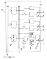
図1は本発明に係る第1の実施形態にかかる液晶表示装置の回路構造の概要を示す等価回路図である。図1において、複数のデータ線対(1−1a,1−1b,1−2a,1−2b…)と複数の走査線2(2−1,2−2…)とが、マトリックス状に互いにほぼ直交して配設されている。このマトリックスの各格子は1画素に対応しており、この格子中には画素を形成するための画素電極3が一つずつ形成されている。なお、図1中では画素電極3自体は表されてされておらず、等価回路的に各液晶セルの図中上側の電極(端子)として表現されている。
【0050】
本実施の形態の液晶表示装置の主要部は、各格子内の一画素ごとに、2つのインバータ素子4,5をループ接続したデジタルメモリセルであるメモリ素子100と、データ線1−1a,1−1b…のように2本ずつ隣り合ったデータ線1−na,1−nb…(nはデータラインの列を示す自然数)とメモリ素子100との間にそれぞれ挿入された2つのnMOS構造のTFT(薄膜トランジスタ)6,7と、交流駆動信号線8(8−1,8−2…)と画素電極3とに接続される一方でゲートが前記のメモリ素子100の一端に接続され、その出力によって制御されて画素電極3に対して交流駆動信号線8の電圧の導通をオン/オフ制御するCMOS構造のトランスファゲート9と、リセット信号線10と画素電極3とに接続される一方でゲートが前記のメモリ素子100の前記とは反対側の一端に接続され、その出力によって制御されて、画素電極3に対してリセット信号線10からの電圧の導通をオン/オフ制御するトランスファゲート11と、画素電極3と対向電極12との間に介挿された液晶層によって形成された液晶セル13とから、構成されている。
なお、交流駆動信号線8およびリセット信号線10は特許請求の範囲では表示制御線として総称され、また、TFTは特許請求の範囲における第1のスイッチ素子に、トランスファゲートは特許請求の範囲における第2のスイッチ素子にそれぞれ対応する。
【0051】
そして対向電極12およびリセット信号線10は、一定電位の電圧を出力する定電圧電源回路(図示省略)に接続されている。またデータ線ドライバ14および走査線ドライバ15が、TFTアレイ基板200の周縁部の上に、各TFTとともにそれらのうちの少なくともいずれか一つのTFTに用いられた材料と同じ材料を用いて配設されている。
【0052】
本実施の形態にかかる液晶表示装置の特に画素部における具体的な回路構造を図3の平面図に、またその断面構造の概要を図3のA−A′断面図である図4に示す。
【0053】
図3および図4によれば、電気絶縁性基板であるガラス基板301上に、p−Si(多結晶シリコン)膜302を活性層として用いて、各画素ごとに画素部スイッチ素子としてのTFT6,7やトランスファゲートを構成する2個一組のTFT9,11やメモリ素子100を構成するTFT等の各種TFT303が形成されている。
【0054】
このp−Si膜302は減圧CVD装置によりa−Si(アモルファスシリコン)薄膜を形成した後、これをアニール炉を用いて600℃の窒素雰囲気中にてアニールすることにより形成した。
【0055】
ゲート絶縁膜304および第1層間絶縁膜305としては、常圧CVD装置により形成したSiOX (酸化シリコン)膜を用いた。ゲート電極306としては低抵抗化を図るためにMoW膜を用いた。そしてソース/ドレイン電極などの電極307はAl膜を用いて形成した。電源線308および接地線309は、プロセス整合性に悪影響の無い範囲で可能な限りの低抵抗化を図るためにAl膜を用いて形成した。
【0056】
また、データ線1(図4中ではデータ線1−1a)は、電源線308との交差部でMoW膜316を経由する構造として形成した。これによりデータ線1全体としての配線抵抗値は若干増大してしまうが、データ信号がデジタル信号であるため書き込み特性に対しては実際上特に問題は生じなかった。
【0057】
交流駆動信号線8およびリセット信号線10は、走査線2にほぼ平行方向の配線としてそれぞれMoW膜を用いて形成した。そして上記のメモリ素子100および交流駆動信号線8などの各種配線の上を第2層間絶縁膜310で被覆して電気絶縁性を確保し、この第2層間絶縁膜の上にAl膜を用いて反射型の画素電極3を形成した。
【0058】
第2層間絶縁膜310は、常圧CVD装置により形成したSiOX (酸化シリコン)膜とプラズマCVD装置により形成したSiNX (窒化シリコン)膜との2層積層構造とした。
【0059】
画素電極3と画素部ごとに形成されたメモリ素子100等の回路素子は、コンタクトホール311を通って電気的に接続されている。
【0060】
一方、第2のガラス基板312上には、ITOのような透明導電膜からなる対向電極12が形成され、さらにそれを含んでガラス基板312の上ほぼ全面を覆うように配向膜313が形成されて、対向基板314の主要部が構成されている。そしてこれら両基板間には、液晶組成物315がその周囲を封止されて注入・挟持されている。
【0061】
上記のような構造は、対向基板314側から光を入射させ、画素電極3上で反射して各画素ごとにその液晶セルにより光変調を行なって、液晶セルから画素電極上での反射光を再び対向基板側へと出射させることで、いわゆる反射型の液晶表示装置として機能するように形成されている。この方式は、メモリ素子100等の回路上に画素電極3を形成できるので、画素電極3の有効面積を、テジタルメモリセル100およびその配線等の占有面積に影響されることなく十分に広く取ることができ、しかもバックライト等も不要であるため、さらに高輝度の(明るい)表示を、さらに低い消費電力で実現できるという、携帯型の液晶表示装置として極めて好適な優れた利点を備えている。
【0062】
本実施の形態においては、画素電極3を反射電極として使う上記のような効果をさらに有効なものとするために、偏光板を用いないで光変調を行なうことが可能なゲスト−ホスト型液晶を液晶組成物として用いた。またゲスト−ホスト型液晶を用いれば、液晶内に混入する色素を種々変更することで、白黒表示の他にも、カラーフィルタを用いることなしにカラー液晶を実現することもできる。このように、ゲスト−ホスト型液晶を用いることにより、光の透過損失が大きく光利用効率を低下させる主因の一つであった偏光板やカラーフィルタが不要となる。
【0063】
次に、この実施の形態に係る液晶表示装置の動作について説明する。
【0064】
この液晶表示装置は、通常の線順次走査を行なうことによってビデオ信号を画面にわたって書き込み動画像表示を行なう駆動モード(順次走査モード)の他にも、画面の一部分のみを選択的に書き換えて表示を行なう部分駆動モード(部分走査モード)や、静止画表示を行なう静止駆動モード(静止画モード)を使い分けることができる。
【0065】
本発明によれば、これらの各モードのうち特に部分走査モードおよび静止画モードにおいて、消費電力を飛躍的に低減することができる。そのような本発明に係る液晶表示装置における1画素へのビデオ信号の書き込みは、以下のようにして実行される。
【0066】
まず、書き込むべき画素に対応した走査線2−n(nは走査線の行を示す自然数)の電位をハイレベルに上げる。これにより走査線2−nに対応する第n行の画素のうちデータ線1−na,1−bにそれぞれ接続している2つのTFT6,7が導通状態となる。
【0067】
そして2本のデータ線1−na,1−nbにビデオ信号を送る。このとき、データ線1−na,1−nbは互いに逆相の信号となるようにする。この状態でデータ線1−na,1−nbからのビデオ信号が2つのインバータ素子4,5で構成されたメモリ素子100に書き込まれる。ただしこの書き込みを可能にするには、TFT6,7を含めたデータ線ドライバ系全体の駆動能力をインバータ素子4,5の駆動能力よりも大きくする必要がある。
【0068】
メモリ素子100の出力は、2つのトランスファゲート9,11にそれぞれその一端ずつが接続されており、メモリ素子100の出力によってトランスファゲート9または11が選択的に導通する。
【0069】
ここで、対向電極12、交流駆動信号線8、リセット信号線10それぞれに印加される電圧の波形を図5の波形図に示す。
【0070】
対向電極12およびリセット信号線10には、電源電圧から供給される電圧の1/2の電位の一定電圧が印加される。
【0071】
トランスファゲート9が選択されている場合には、画素電極3には交流駆動信号が印加されて、液晶セル13にピーク値V0 の交流的な液晶印加電圧が印加される。一方、トランスファゲート11が選択されている場合には、液晶セル13に電圧は印加されない。そしてこのような液晶セル13への液晶印加電圧の有/無で液晶分子の配向状態が変化して画素の明暗が制御され、表示が行なわれる。
【0072】
このような動作で1画素の書き込みを行なう。そして順次走査モードにおいては、データ線ドライバ14を例えば左から右へと駆動する一方、走査線ドライバ15を例えば上から下へ線順次に駆動することにより、画面内の全画素にわたって上記動作を繰り返して1フレーム(あるいは1フィールド)の画面の書き込みを行なう。いわゆる動画表示を行なう場合には、このような順次走査モードで前記画面内の画素にわたって書き込みおよび表示を行なう。
【0073】
これに対して、表示画像が部分的にのみ変化する場合(例えばマウスポインタや点滅するカーソル等)には、部分走査モードを用いる。
【0074】
この部分走査モードでは、画面上の書換えが必要な部分のみに選択的に書き込みを行なう。一般的ないわゆるダイナミック駆動型の液晶表示装置では、画素スイッチや液晶セル(の容量)自体のリーク電流等に起因して画素電位が時間とともに変化するため、画素に書き込まれるデータ自体は同じでも一定の期間(一般に1/60秒)ごとに再書き込みが必要であった。しかし本発明によれば、画素電位は交流駆動信号またはリセット信号と同一となり、時間的に変化しないので、データ自体に変化が無い場合には再書き込みを行なうことが不要となる。
【0075】
従って、表示画像の一部のみが変化する表示を行なう場合には、その変化する部分のみのデータの書き換えを行なうだけでよくなるのでデータの転送速度を落とすことができるとともに消費電力の大幅な低減を図ることができる。
【0076】
そのような部分走査を行うデータ線ドライバ14および走査線ドライバ15の例を、図2の等価回路ブロック図で示す。このような、デコーダ型の液晶駆動回路系を用いることで行なう。即ちこのようなデコーダ型の液晶駆動回路を用いることにより、表示の変化に関与する電圧の書き換えが必要な任意の画素に対応したデータ線および走査線を選択することができ、その特定の画素だけに選択的に新たな書き込みを行なうことができる。
【0077】
図2に示すように、データ線ドライバ14は、アドレス信号を入力するデコーダ回路201、そのデコーダ回路201の出力によって制御されるスイッチ素子202、このスイッチ素子202を介してビデオ信号線203に接続されるデジタルラッチ回路204、このデジタルラッチ回路204に接続されたバッファ回路205(バッファ回路205a,b)、そしてこれらバッファ回路205の出力を制御する出力制御回路206とから、その主要部が構成されている。
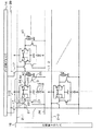
【0078】
アドレス信号により特定のビットが選択されると、ビデオ信号線203からスイッチ素子202を経由してデジタルラッチ回路204にビデオ信号が入力され、さらにバッファ回路25a,bを通ってデータ線1−na,1−nbに出力される。
【0079】
出力制御回路206は、アドレス信号で選択されたビットのバッファ回路205a,bのみを働かせ、選択されていないビットについてはバッファ回路205a,bの出力をハイインピーダンスに保持する回路で、バッファ回路205a,bの出力をハイインピーダンスにすることで、それが出力されるデータ線1−na,1−nbに対応した画素部のTFT6,7が導通状態でもメモリ素子100に保持されたデータの状態は変わることなく保てるようにしている。
【0080】
静止画表示を行なう場合には、上記のような部分走査も不要なので、データ線ドライバ14および走査線ドライバ15を止めて交流駆動信号のみを入力することで、表示を行なうことができる(静止画モード)。
【0081】
このとき、交流駆動信号の周波数は、通常のフレーム書き込みの周波数として用いられる60Hz程度でもよく、あるいはフレーム書き込みの周期はさらに長くすることもできる。また、フレーム書き込みの周波数を60Hzとした場合でも、対角6インチの液晶表示装置の消費電力は1mW以下となる。これは、従来の一般的なダイナミック駆動方式の液晶表示装置と比べて1/100〜1/1000であり、飛躍的な消費電力の低減が実現できることが分かる。
【0082】
図6〜図8は静止画表示時に交流振動周波数を落として用いる本発明にかかる液晶表示装置の第2の実施の形態を示すもので、図6は回路構成ブロック図、図7はその動作を示すタイミングチャート、図8は図6における交流駆動信号発生回路(特許請求の範囲における周波数変更手段に相当する)の回路構成ブロック図である。
【0083】
図6によれば、液晶表示装置200は表示部150とこの表示部150を制御する走査線ドライバ15、データ線ドライバ14を有している。走査線ドライバ15は走査線ドライバ入力信号をもとに走査線の制御を行い、データ線ドライバ14はデータ線ドライバ入力信号をもとにデータ線の制御を行うものであり、動画表示時には通常の液晶表示装置と同様に交流信号の周波数をフレーム周波数と同一にする。走査線ドライバ15は走査線信号発生回路50および交流駆動信号発生回路60からなっており、交流駆動信号発生回路60は走査線ドライバ入力信号およびデータ線ドライバ入力信号により静止画表示時に交流反転周波数を動画表示時の1/5に切り換えるものである。
【0084】
この交流駆動信号発生回路50は、図に示すように、基本クロックを発生する水晶発振子等の発振回路51、この発振回路で発生した基本クロック信号から複数の異なる分周クロック信号を発生させる各種カウンタよりなる分周回路52、アドレス信号が変化しているか否かをその立ち上がりあるいは立ち下がりで検出するラッチ回路等のアドレス信号検出回路53、このアドレス信号検出回路53の出力信号およびそのインバータ54による反転信号により制御され、複数のクロック信号のいずれかを選択するスイッチ回路55を有している。
【0085】
この実施の形態における動作は、図7に示すように、例えば、分周クロック信号として30Hz(1/2周期が1/60秒)および6Hz(1/2周期が1/12秒)の方形波を準備し、アドレス信号が変化している動画表示時には30Hzのクロック信号を選択し、アドレス信号が停止している静止画表示時には6Hzのクロック信号を選択するようにする。
【0086】
このような制御を行うことにより、消費電力を著しく低減することができる。
【0087】
この実施の形態においては、走査線ドライバ回路中の交流信号発生回路でクロック信号を発生させているが、交流信号発生回路の機能を外部のディスプレイコントローラに持たせ、その出力である走査線ドライバ信号として走査線ドライバに供給することができる。
【0088】
次に、交流駆動信号線8(8−1,8−2,…8−n…)は、それら全ての交流駆動信号線8を同一のタイミングで極性反転させてもよいが、瞬時電流を抑えるためにはタイミングをずらせて反転させることが効果的である。これは、例えば交流駆動信号線8を上から順に走査するという方法で実現できる。そのような交流駆動信号の一例を図9に示す。
【0089】
図9によれば、各走査線2−nごとにそれぞれ対応した交流駆動信号線8−1,8−2,…8−n…には、それぞれΔt間隔でタイミングをずらせた交流信号が印加されており、この交流信号の立ち上がりおよび立ち下がり時に、各交流駆動信号線8−nに接続された液晶セル13ごとへの書き込みが各々行なわれる。従って、表示領域中のすべての液晶セル13に対して同時に書き込みを行なうことは無くなるので、大きな瞬時電流が流れることを避けることができる。
【0090】
ただし、このとき、静止画モードでも走査線ドライバの一部は動作するので、その分は完全な静止画像表示時と比べれば消費電力が増大する。しかし、その動作速度は十分に遅くてもよく、またそのとき駆動される画素数も少ないので、実質的には前記のような消費電力の増大分は極めて小さく、液晶表示装置全体の消費電力においては無視できる程度の量である。
【0091】
なお、上述したような本実施の形態では、いわゆる画素部スイッチング用の素子である画素部TFT6,7として、互いに逆相のデータ線に接続された2個のnMOS−TFTを用いているが、本発明はこのような本実施の形態のTFTのみには限定されない。この他にも、画素部スイッチング用素子として1個のトランスファゲートを用いてもよく、または単一のTFTを用いてもよい。あるいはTFT以外でもスイッチング素子として上記のTFTを用いてなるスイッチ素子と回路的に等価である素子を用いてもよい。
【0092】
また、上記実施の形態のTFTを組み合わせて形成されたトランスファゲート9,11は、TFTの他にもこれと回路的に等価である素子を用いてもよい。
【0093】
以上のように、本発明の液晶表示装置においては、従来とは異なり、対向電極の電位を一定電位に保ったまま液晶セルを交流的に駆動することができるので、従来の液晶表示装置においては必要だった大容量の(例えば対角6インチの液晶表示装置で0.2μF程度)の液晶ドライバ回路系は必要なく、飛躍的に小容量な液晶ドライバ回路による駆動が可能となる。
【0094】
従って、液晶ドライバ回路系の構造の簡潔化および小型化や、その製造方法の簡易化、そして液晶表示装置としての消費電力のさらなる低減化等を実現することができる。
【0095】
なお、上記実施の形態は、反射型構造の液晶表示装置に本発明の技術を適用した場合について述べたが、画素サイズが比較的大きく画素内の回路領域を除いた領域に十分な画素開口部(1画素ごとの十分な画素面積)を確保できる場合には、透過型構造の液晶表示装置に本発明の技術を適用することで、上記実施の形態と同様の効果を得ることができる。
【0096】
図10は本発明に係る液晶表示装置の第3の実施の形態における回路構造の概要を示す図である。この図では図1と同じ構成要素には同じ符号を付すこととする。
【0097】
図10において、複数のデータ線1−1,1−2・・・および複数の走査線2−1,2−2・・・がマトリックス状に配設されている。そのマトリックスの各格子は1画素に対応しており、この格子中には1画素を形成するための画素電極3が一つずつ形成されている。なお、図中では画素電極3自体は表されておらず、各液晶セルの上側の電極(端子)として表現されている。
【0098】
データ線1−1,1−2・・・はデータ線ドライバ14により制御されるデータ線選択用のTFT17を介してビデオ信号線29と接続され、走査線2−1,2−2・・・は走査線ドライバ15により駆動される。これらのドライバは一般に用いられているシフトレジスタ型の駆動回路で構成される。
【0099】
データ線1−1,1−2・・・には画素部TFT21のドレイン電極が接続され、ソース電極はメモリ素子110に接続されており、その画素部TFT21のゲート電極は走査線2に接続されて、画素部TFT21の導通/非導通は走査線2−1,2−2・・・によって制御される。
【0100】
メモリ素子110は、図10に示すように、TFT22およびTFT23を組み合わせてなるCMOSインバータと、TFT24およびTFT25を組み合わせてなるCMOSインバータとの2つを組み合わせて形成されている。
【0101】
TFT22およびTFT23を用いてなるインバータの出力(ソースおよびドレイン側)は、TFT24およびTFT25を用いてなるインバータの入力(ソースおよびドレイン側)と接続されており、かつその一方でそのゲート側は、特許請求の範囲で表示制御線に相当する極性切り替え信号線26−1に接続されて制御される2個一組のスイッチTFT27、スイッチTFT28のうちのスイッチTFT28を介して、液晶セル13の画素電極3に接続されている。
【0102】
また、TFT24およびTFT25を用いてなるインバータの出力は、TFT22およびTFT23からなるインバータの入力と接続されており、かつその一方でそのゲート側は、極性切り替え信号線26−1に接続されて制御される2個一組のスイッチTFT27およびスイッチTFT28(特許請求の範囲で第2のスイッチ素子に相当する)のうちのスイッチTFT27を介して、液晶セル13の画素電極3に接続されている。そして、液晶セル13の他端(図中下側の電極(端子))は、対向電極12に接続されている。
【0103】
このように、この実施の形態に係る液晶表示装置の構造は、各画素部に配設されたスタティック型のメモリ素子110の構造およびその信号読み出し部(画素電極への信号書き込み部)の構造を、極性切り替え信号線26とこの信号線26により制御される極性の相異なる2個一組のスイッチTFTとで形成しているので、従来のスタティック型の液晶表示装置と比べて極めてシンプルな構造となっている。本発明に係る液晶表示装置は、メモリ素子110を含んで1画素あたりわずか合計7個のスイッチTFTを用いて形成することができ、前述した11個のスイッチTFTが必要な従来の場合と比べて、大幅に小型化することができる。
【0104】
この実施の形態に係る上記のような回路構造の液晶表示装置の一例として、640×480ドットのVGA液晶表示パネルの場合を例にとり、その画面全体に用いられるTFTの個数を従来の液晶表示装置と比較すると、全体で60万個以上(全体の約30%減以上に該当)のTFTを減少させることができた。
【0105】
従って、従来の液晶表示装置と比べて、飛躍的にその回路構造およびその物理的構造を大幅に簡易化することができ、その結果、製造歩留まりも大幅に向上する。
【0106】
このような利点は、例えばハイビジョン用の液晶表示装置のように表示画素数のさらなる多画素化および高精細化が進むほど、さらに効果を発揮する。換言すれば、従来の液晶表示装置では、さらなる多画素・高精細化あるいは各画素部の微細化は限界に来ておりそれへの対応は実際上不可能であったものが、本発明によれば、さらなる多画素・高精細化や画素部の微細化を実現することができる。
【0107】
次に、上述のような本発明に係る第3の実施の形態の液晶表示装置の動作について説明する。
【0108】
動画像表示時には、走査線ドライバ15が、1走査タイミングごとに例えば画面の上側から下側へと線順次に走査線2を1本ずつ選択し、各行ごとの画素部TFT21を順次導通状態にして行く。
【0109】
次に、ビデオ信号をビデオ信号線29に入力し、基準クロック信号と同期しつつデータ線ドライバ14によりデータ線選択用のTFT17を導通させて、画素部TFT21を介して、メモリ素子110のノード31側にビデオ信号を書き込む。
【0110】
このとき、極性切り替え信号線26をハイレベルの一定電位とし、極性切り替えのための2個一組のうちの一方のスイッチTFT27側だけを導通状態にして、液晶セル13の画素電極3に印加電圧の書き込みを行なう。
【0111】
このような印加電圧書き込み動作を、各走査線2上の各画素について、その走査線2の一端から他端へと順次に行なう。このような印加電圧書き込み動作を各走査線2について行なうことにより、画面の表示領域全ての画素について所望のビデオ信号を書き込むことができる。
【0112】
また、よく知られているように一般に液晶セルは直流電流の印加に起因した液晶層の劣化を避けるために交流的に駆動される。そこで、上記とは逆極性の電圧書き込み時には、ビデオ信号を極性切り替え信号線26により制御されるスイッチTFT28を介して液晶セル13の画素電極3に書き込みを行なう。そして極性切り替え信号線26をロウレベルの電位に固定しておいてメモリ素子110の上記で用いたインバータとは反対側のTFT24、25よりなるインバータにより反転してノード31側とは逆極性のノード32側の信号(電圧)を、スイッチTFT28を介して液晶セル13の画素電極3に書き込む。
【0113】
次に、静止画像表示時の、本実施の形態に係る液晶表示装置の動作を説明する。
【0114】
画素部TFT21はnチャネル型で形成されており、走査線ドライバ15によって、ある走査線2に対して正のパルスを印加し、その走査線2にゲートが接続された全ての画素部TFT21を導通状態にする。
【0115】
その状態で、さらにデータ線ドライバ14によってデータ線選択用のTFT17が導通状態になると、ビデオ信号線29の電位がメモリ素子110にそのノード31側から書き込まれる。このとき、データ線1の電位がハイレベルであれば、ノード31側にはハイレベルの信号(電圧)が書き込まれ、ノード32にはロウレベルの電位が書き込まれる。これらの電位は、画素部TFT21を介してデータ線1からロウレベルの電位が書き込まれるまで変化せずに前記のメモリ素子110によって保持される。
【0116】
メモリ素子110のノード31側の電位がハイレベルのときには、極性切り替え信号線26の電位をハイレベルにすると、nチャネル型のTFT27が導通状態となり、画素電極3にノード31側のハイレベルの電位が書き込まれる。
【0117】
また、極性切り替え信号線26の電位をロウレベルにすると、pチャネルTFT28が導通状態となってノード32側のロウレベルの電位が画素電極3に書き込まれる。
【0118】
ここで、極性切り替え信号線26の電位レベルを所定の時間間隔ごとにハイ/ロウと交互に変化させるとともに、これに合せて対向電極12の電位(電圧レベル)をロウ/ハイと交互に切り替えることにより、静止画像表示時においてデータ線1の電位は全く書き換えることなく液晶セル13を交流駆動することができ、液晶表示装置としての低消費電力駆動が可能となる。
【0119】
従って、ビデオ信号を画面全体の画素電極全てに一旦書き込んでしまえば、データ線ドライバ14および走査線ドライバ15自体は全く駆動させなくとも、またビデオ信号線15からのビデオ信号を止めても、常に静止画像表示が可能となる。ここで、本実施の形態の場合には、液晶表示装置がノーマリーホワイトモードのときには、極性切り替え信号線26と対向電極13が両方ともハイレベルまたはロウレベルで白表示、片方がハイレベルでもう一方がロウレベルなら黒表示、のような表示方式となる。
【0120】
画素部TFT21の導通時にビデオ信号線15から供給されるビデオ信号(電圧)の電位つまりデータ線1の電位がロウレベルの際には、ノード31側がロウ電位に落ちる一方ノード32側がハイレベルになる。
【0121】
そして画素部TFT21が非導通状態になると、メモリセル110のデータは次の書き込みが行なわれるまでメモリ素子110によって保持される。
【0122】
そこで前述したのと同様に極性切り替え信号線26および対向電極12の電位レベルをハイ/ロウと交互に変化させることで、液晶セル13を交流駆動することができる。
【0123】
図11は、本発明に係る第3の実施の形態の液晶表示装置を静止画像表示させる時の印加電圧波形を示すタイミングチャートである。液晶表示装置がノーマリーホワイトモードであるとして、図11(a)の場合には極性切り替え信号線26と対向電極12が両方ともハイレベルまたはロウレベルで黒表示となり、図11(b)の場合には片方がハイレベルでもう片方がロウレベルの場合には白表示となる。
【0124】
データ線1を制御するデータ線ドライバ14及び走査線ドライバは、画素部TFT21などの各種素子や走査線2などの配線等と同様の材料および製造プロセスを用いて、それらと同時に形成することが望ましい。また前記の走査線2を制御する走査線ドライバも同様に画素部TFT21や走査線2などの配線等と同様の材料および製造プロセスを用いて、それらと同時に形成することが望ましい。
【0125】
このようにデータ線ドライバ14および走査線ドライバ15のような液晶駆動回路系を、画素部TFT21と同様な材料および製造プロセスを用いて同時に形成することで、液晶駆動回路系を液晶駆動ICのような外付け回路として外付けする必要がなくなり、構造が簡易化され、製造方法の簡易となり、コスト的にもさらに有利なものとなる。また外付けの液晶駆動ICのような外部駆動回路とのインターフェースに制約されることなく画素ピッチ等の仕様を自由に設定できるという大きな利点も得ることができる。
【0126】
ところで、走査線2により制御される画素部TFT21の電流駆動能力をG1、メモリ素子110の構成要素であるTFT22、23、24、25の電流駆動能力をG2、極性切り替え信号線26により制御される2個一組のTFT27、28の電流駆動能力をG3とすると、G1>G2>G3となるようにすることが望ましい。
【0127】
何故なら、ノード31側の電位は、走査線2により制御される画素部TFT21とメモリ素子110のTFT22、23、24、25との電位の引き合いの量できまるためである。つまり、ここで仮に走査線2により制御される画素部TFT21の電流駆動能力G1がメモリ素子110のTFT22、23、24、25の電動駆動能力G2よりも小さいと、データ線1の電位がノード31側に書き込めなくなる。また、極性切り替え信号線26により制御される2個一組のTFT27、28の電流駆動能力G3がメモリ素子110の構成要素であるTFT22、23、24、25の電流駆動能力G2よりも大きいと、液晶セル13の画素電極3にデータ(ビデオ信号)を書き込む際にメモリ素子110の保持データが破壊されて(あるいは乱され変化して)しまうからである。
【0128】
次に、本発明の第3の実施の形態の液晶表示装置における特に画素部の構造を図12および図13に基づいて説明する。
【0129】
図12は、画素部TFT21をはじめとして各TFTにp−SiTFTを用いた反射型の液晶表示装置の一画素部分の回路パターンを示す平面図である。また図13はその断面構造を示す図である。
【0130】
図12に示すように電源線301(Vdd)、電源線302(Vss)およびデータ線1によって囲まれた領域内に画素電極3が配置されて各画素領域が形成されている。その画素電極3の下には、走査線2、極性切り替え信号線26、画素部TFT21、メモリ素子110を構成する素子であるTFT22、23、24、25、2個一組のスイッチTFT27、28およびそれらの間を接続する配線が形成されており、電気絶縁層401を介して画素領域ほぼ全面が画素電極3に覆われている。
【0131】
一方その断面構造は、図13に示すようにガラス基板402上にはp−Si膜403が形成されており、TFT22、23、24、25はいずれも、p−Si膜403上に薄膜でゲート酸化膜404を形成し、さらにその上にゲート電極405を形成してなるMOS構造のTFT素子である。それらのソース電極およびドレイン電極はそれぞれAl−Si膜406からなる電極であってp−Si膜403の上に、オーミックコンタクトされている。
【0132】
p−Si膜403は、減圧CVD法でガラス基板402上にa−Si(アモルファスシリコン)膜を成膜した後これをエキシマレーザでアニールしてp−Si化することにより形成されている。
【0133】
ゲート酸化膜404は、CVD法により形成されたSiO2 膜からなる。ここで、ゲート電極405の材料は配線抵抗を少なくするためにWSix (タングステンシリサイド)膜とp−Si膜との2層積層構造とした。
【0134】
上記の各p−SiTFTの仕様は、pMOSTFTはチャネル長L=4.5μm、チャネル幅W=8μmとし、nMOSTFTはチャネル長L=6μm、チャネル幅W=8μmとした。
【0135】
反射型の画素電極3はAlを材料として形成され、コンタクトホールを通ってスイッチTFT10、11に接続されている。そして画素電極3と対向電極12との間にはポリマー分散型の液晶層407が注入・封止されて、偏光板の不要なポリマー分散方式の液晶表示パネルとして形成されている。なお、本実施の形態では液晶材料として高分子樹脂に液晶をドロップレット状に分散してなるポリマー分散型の液晶を用いたが、この他にも例えば染料を混入させたゲスト−ホスト型の液晶組成物等を用いても良い。
【0136】
図14は、本発明に係る液晶表示装置の第4の実施の形態の回路構造の概要を示す図である。
【0137】
この実施の形態の液晶表示装置においては、画素部の回路構成は上述の第3の実施の形態と全く同様であるが、データ線1および走査線2を駆動する液晶駆動回路系として、第3の実施の形態のシフトレジスタ型とは異なりデコーダ型の液晶駆動回路系を用いた点が異なる。すなわち、図14に示すように、画素が配列された画面表示領域の周辺部分に配置されたデコーダ型の液晶駆動回路系つまりデータ線ドライバ501および走査線ドライバ502が配置されており、これらのデコーダ501,502は、各データ線、アドレス線の各アドレスに対してそのアドレスに合致した信号で活性化信号が得られるような論理回路が設けられている。
【0138】
具体的には、データ線ドライバ501は10ビットの信号(0000000000、0100100111など)が入力されると、その信号に対応したデータ線1に対して「1」を出力しその特定のデータ線1を選択状態とする。走査線2の側も同様に、9ビットの信号入力を受けてその信号に対応した走査線2を選択状態にする。
【0139】
通常は、走査線2もしくはデータ線1を端から順にアドレスするように数値信号を入力するが、その数値信号を適当に設定することで画像が変化しない表示部の画素には書き込みを行なわずにそれまでの印加電圧の状態を保持し、画像が変化する画素にだけ新たに電圧の書き込みを行なうことが可能となる。これにより、データ線1および走査線2を駆動する液晶駆動回路系にシフトレジスタ型を用いた先の第3の実施の形態よりも、さらなる低電力化を実現することができる。
【0140】
一例として、アスペクト比4:3の通常のテレビ画面中にアスペクト比16:9のワイド画面を表示するビスタ表示の場合について考える。
【0141】
図15(a)は画面90のフルサイズで動画像を表示する場合の通常の画面の走査の様子を示しており、走査線ごとに左端から右端まで移動して次の走査線に移る様子が示されている。また、図15(b)はビスタサイズで動画像表示を行なう場合の画面の走査の様子を示しており、画面の縦横アスペクト比の違いに起因した走査線本数を適合させるために上下に黒い非表示部91、92を生じさせる必要があることを示している。このような黒い非表示部は、本発明によれば、その該当箇所の画素に一旦黒を書き込めばその画素のメモリ素子110によってその電位を保持して、液晶表示装置の電源オフまでは新たな書き込みあるいは電圧の変化は行なわない。そして画面中央の表示部にだけビデオ信号の書き込み走査を繰り返して、その部分の画像をビデオ信号に従って変化させて動画の画像表示を行なうことができる。ビスタ表示よりも横長のシネマスコープ表示の場合は黒画素部の比率はさらに高くなる。
【0142】
本発明によれば、このような動作を可能とすることによって、シフトレジスタ型の液晶駆動回路系を用いた本発明の第3の実施の形態よりさらに一層の低消費電力化を図ることも可能である。
【0143】
図16は、本発明による液晶表示装置のさらに別の第5の実施の形態の回路図である。この図においてもこれまでの実施の形態と同じ構成部分には同じ参照番号を付し、詳細な説明を省略することとする。
【0144】
この実施の形態は先の第3の実施の形態とデータ線1、走査線2、液晶セル13、データ線ドライバ14、走査線ドライバ15、TFT21、メモリセル110、スイッチ27、28などの構成は全く同じである。異なるのは、ノード32に光電変換素子40の一端が接続されている点である。この光電変換素子40の他端はGNDに接地されている。
【0145】
次に、この実施の形態の動作について説明する。
【0146】
動画像表示時の動作および静止画表示時の動作は第3の実施の形態の場合と全く同じであるので省略し、本実施の形態に特徴的である、画像入力時の動作について説明する。
【0147】
まず、データ線ドライバ14及び走査線ドライバ15を停止させる。図中のある画素内の光電変換素子40に特定波長及び強度の光が光入力手段、例えばライトペンにより照射されるとノード32は光電変換素子40が導通することからロウレベル(GND)電位になる。メモリはフリップフロップ型であるので、逆側のノード31はハイレベル電位となる。
【0148】
ここで極性切り替え信号線26の電位及び対向電極12の電位を互いに逆位相となるように変化させておくと液晶層に電圧がかかり、ノーマリーホワイトモードのときには白表示だったものが黒表示に変わる。すなわち画素内の光電変換素子40に光が照射された画素のノード31はハイレベル電位となって黒くなる。また、始めから黒表示の場合はそのまま変化しない。
【0149】
光入力手段による入力動作が終了したらデータ線ドライバ14及び走査線ドライバ15を動作させて各画素のノード31のデータを読み込むことにより、入力データをビデオRAMに取り込むことができる。
【0150】
データ線1を制御するデータ線ドライバ14は、画素部のスイッチTFTや配線等と同様のプロセスを用いてそれらと同時に形成する。また走査線2を制御する走査線ドライバ15も同様に、画素部のスイッチTFT27,28や配線等と同様のプロセスを用いて同時に形成する。このように、ドライバを画素部と同様なプロセスを用いて同時に形成することで駆動用ICを外付けする必要がなくコスト的に有利になる。また、外部駆動回路とのインターフェースを考慮することなく、画素ピッチを自由に設定できるという利点がある。
【0151】
図17に、この実施の形態をスイッチ素子にポリシリコンTFTを用いて実現した反射型液晶表示装置の断面概略図(部分)を示す。ここに示された断面構造は図13に示したものと類似するので、同じ部分には同じ番号を付してその詳細な説明は省略する。
【0152】
アルミによる反射画素電極3’は、コンタクトホール406を介してスイッチ素子と接続されているが、素子形成部を含んで絶縁膜401の上に広く形成されており、光電変換素子40の形成部分のみ開口部41が設けられている。
【0153】
光電変換素子40は他のスイッチ素子と同様な構造で作られている。対向電極12’にはこの光電変換素子40に対応するように開口部42が形成されており、ライトペン等の光入力手段43により光が照射され、光電変換素子40に光が到達すると、そのソース/ドレイン間が導通するようになっている。
【0154】
図18に本発明による液晶表示装置の第6の実施の形態の回路図を示す。
【0155】
この実施の形態によれば、先の第1の実施の形態と走査線2、液晶セル13、データ線ドライバ14、走査線ドライバ15、TFT21、メモリセル110、スイッチ27、28などの構成は全く同じであるので、その詳細な説明は省略する。異なるのは、データ線が1アドレスあたり書き込み用と読み出し用の2本(例えば1−1a、1−1b)となっており、それぞれデータ線選択用のTFT17−1、17−2により選択されるようになっている点と、ノード32に接続された位置検出回路60と、ビデオRAMが書き込み用と読出し用の2つ(72,73)設けられている点と、これらの比較を行う比較器73が設けられている点である。
【0156】
この位置検出回路60は、電源と接地間に自己バイアスされたトランジスタ62に直列に接続された第1の光電変換素子61、この光電変換素子61とトランジスタ62との接続点とノード32にそれぞれ入力端子が接続されたエクスクルーシブORゲート63、その出力端子に接続された第2の光電変換素子64、その出力側に設けられたループ接続された2つのインバータ65、66よりなるフリップフロップメモリ、その出力側とデータ線1−1bとの間に接続され走査線2−1にゲートが接続されたスイッチTFT69を有している。
【0157】
デジタルメモリ及び画素電極への書き込みは第3の実施の形態と同様であるので省略し、ここではデータの入力方法について説明する。
【0158】
今、ノード80のデータをA、ノード32のデータをB、ノード67のデータをC、ノード68のデータをD、ノード31のデータをXとすると論理値表は以下のようになる。
【0159】
表
A B C D X(=B*)
0 0 0 1 1
0 1 1 0 0
1 0 1 0 1
1 1 0 1 0
なお、*は反転を表す。
【0160】
上の表でA=0は画素に光が照射されておらず、光電変換素子の抵抗値が高く、トランジスタ62により接地電位に引き下げられた状態を示している。このときB*=Dが成り立つ。故にD(ノード68のデータ)とX(ノード31のデータ)を比較するとD=Xとなり、等しい。
【0161】
次にA=1、即ち光が画素(内の素子)に照射された状態のときを考える。A=1の際には、B=D=X*が成立する。故にノード68にはノード31と逆極性のデータが現れる。その後、光が照射されなくなってもデータはメモリに保存される。そこでノード68のデータを読出し用のビデオRAM72に記憶させ、これと始めにノード31に書き込まれ、書き込み用のビデオRAM71に記憶されたデータとを比較回路73で比較することで画面中のどの位置でデータ内容が変化したかが把握でき、画面上での画素単位の正確な入力が可能となる。ビデオRAM72のデータを新たにデータ線1−1aを介して画素電極に書き込めば入力情報を表示する事も可能となる。
【0162】
なお、このような入力を行う場合、光検知による反転と交流駆動による反転とが同時に起こり、入力が正確に行えない可能性がある。これを防止するためには、ライトペンの発光を交流とは逆相にしておけばよい。
【0163】
また、この入力を屋外で行う場合、強い太陽光のために、誤入力を招くおそれもある。これを防止するには、光電変換素子の感度を赤外線領域で高めておき、ライトペンの発光手段を赤外線発光素子とすればよい。
【0164】
以上説明した、本発明にかかる液晶表示素子の第4あるいは第6の実施の形態では、反射型構造となっているが、本発明は透過型構造としても良い。しかし、次の理由から反射型構造の液晶表示装置とすることが望ましい。
【0165】
例えば、本実施の態様による液晶表示装置を透過型構造として、チャネル長L=4.5μm、チャネル幅W=8μmのpMOSTFTおよびチャネル長L=6μm、チャネル幅W=8μmのnMOSTFTを用いて6インチVGA単板カラー液晶表示パネルを形成するような場合などには、開口率が20%程度しかとれず表示が暗くなってしまう。
【0166】
そこで、本発明による液晶表示装置を反射型構造で画素電極をスイッチTFT、極性切り替え線等の上に絶縁体を介して設置することで、画素電極が素子数の多さやサイズに制約されずに広くとれ、実効開口率80%以上と大きく設計できるので明るい表示が可能となる。
【0167】
即ち、図13あるいは図17の断面図にその構造の概要を示すように、画素電極3を上記の各TFT22、23、24、25や極性切り替え信号線26等の上に電気絶縁層401を介して設置することで、各画素ごとにTFTの合計素子数に対応した占有面積の大きさや配線に要する面積の広さに制約されることなく画素電極3の有効面積を広く取ることができる。その実効開口率は実際上、80%以上と、飛躍的に大きく設計できるので、高輝度の表示が可能となる。しかも、このように本発明による液晶表示装置を反射型構造とすることで、静止画像表示時は省電力動作が可能なうえにバックライトが不要となるので、液晶表示装置全体としての消費電力をさらに大幅に抑えることができ、ノートブック型パソコンのようなバッテリー駆動方式で駆動される携帯用情報処理装置などに特に好適である。
【0168】
本発明による液晶表示装置を反射型構造とすることで、一画素中に繁雑な多数のTFTを用いた回路を収めるように形成することが可能となり、静止画像表示時は省電力動作が可能なうえ、バックライトが必要ないのでさらに消費電力が抑えられ、携帯用の小型情報端末等のバッテリー駆動に大変都合がよい。本発明を例えば6インチのVGA液晶表示パネルに適用した場合には、液晶表示パネル自体の消費電力は1mW以下となり、飛躍的な低消費電力化を達成できる。
【0169】
【発明の効果】
本発明によれば、画素内にメモリセルを有し、このメモリセルの記憶内容に応じて表示制御線と画素との接続を制御するスイッチ手段を有しているため、表示の変化に関与する電圧の書き換えが必要な画素に対応したデータ線あるいは走査線を選択することができ、特に静止画像表示時の消費電力を減少させることができ、また、データ線あるいは操作線のアドレス変化を検出し、アドレス指定が行われず新たな表示データが与えられないときには交流駆動信号の周波数を低下させるようにしているので、消費電流をさらに低下させることができ、携帯型情報処理装置に好適な液晶表示装置を提供することができる。また、液晶ドライバを少ない素子で形成できるため、回路構造および物理的構造を簡略化でき、小型の液晶表示装置を、高い歩留まりで実現することができる。
【0170】
このような構成は反射型のセル構造を採用し、駆動回路を一体的に形成することにより小型化に有効である。
【図面の簡単な説明】
【図1】本発明による液晶表示装置の第1の実施の形態の回路図。
【図2】第1の実施の形態におけるデータ線ドライバおよび走査線ドライバの例を示す回路ブロック図。
【図3】本発明の第1の実施の形態にかかる液晶表示装置の画素部における具体的な回路構造を示す平面図。
【図4】図3のA−A′断面図。
【図5】第1の実施の形態において、対向電極、交流駆動信号線、リセット信号線にそれぞれに印加される電圧の波形を示す波形図。
【図6】静止画表示時に交流駆動周波数を落として用いる本発明による液晶表示装置の第2の実施の形態の概略回路構成ブロック図。
【図7】図6の構成における動作を示すタイミングチャート。
【図8】図6における交流駆動信号発生回路の詳細な構成を示す回路構成ブロック図。
【図9】瞬時電流を抑えるためにタイミングをずらせて反転させるべく、交流駆動信号線を順に走査した様子を示すタイミングチャート。
【図10】本発明による液晶表示装置の第3の実施の形態における回路構造の概要を示す回路図。
【図11】第3の実施の形態の液晶表示装置を静止画像表示させる時の印加電圧波形を示すタイミングチャート。
【図12】本発明による液晶表示装置の第4の実施の形態における画素部の構造を示す平面図。
【図13】図12の断面構造を示す断面図。
【図14】本発明に係る液晶表示装置の第4の実施の形態における回路構造の概要を示す回路図。
【図15】通常のテレビ画面をビスタサイズで用いる場合の非表示部を示す説明図。
【図16】入力機能を有する本発明による液晶表示装置の第5の実施の形態における回路構造の概要を示す回路図。
【図17】第5の実施の形態をスイッチ素子にポリシリコンTFTを用いて実現した反射型液晶表示装置の断面概略図。
【図18】本発明による液晶表示装置の第6の実施の形態の回路図。
【図19】一般的な従来の液晶表示装置の回路構造の概要を示す図。
【図20】従来のスタティック型の液晶表示装置の回路構造の第1の例を示す回路図。
【図21】従来のスタティック型の液晶表示装置の回路構造の第2の例を示す回路図。
【符号の説明】
1 データ線
2 走査線
3 画素電極
4,5 インバータ
6,7 TFT
8 交流駆動信号線
9,11 トランスファゲート
10 リセット信号線
12 対向電極
13 液晶セル
14 データ線ドライバ
15 走査線ドライバ
21 画素部TFT
22,23 インバータ素子
26 極性切り替え信号線
27,28 スイッチTFT
40 光電変換素子
41,42 開口部
50 走査線信号発生回路
51 発振回路
52 分周回路
53 アドレス信号検出回路
54 インバータ
55 スイッチ
60 交流駆動信号発生回路
71,72 ビデオRAM
73 比較回路
100,110 メモリセル
201 デコーダ回路
202 スイッチ
204 デジタルラッチ回路
205 バッファ回路
206 出力制御回路
501 データ線デコーダ
502 走査線デコーダ[0001]
BACKGROUND OF THE INVENTION
The present invention relates to a liquid crystal display device, and more particularly to a liquid crystal display device suitable for a display device of a small information terminal such as a portable personal computer and capable of realizing high-definition image display with low power consumption.
[0002]
[Prior art]
Liquid crystal display devices are widely used as image display devices for various information processing devices, portable televisions, wall-mounted televisions, and the like as display devices that replace cathode ray tubes (CRTs). In particular, in recent years, it has been attracting attention as a display device that can be reduced in thickness and weight, and is used in portable information processing devices such as so-called notebook computers.
[0003]
Among such liquid crystal display devices, a thin film transistor (hereinafter abbreviated as TFT) such as a thin film transistor (hereinafter abbreviated as TFT) formed of polycrystalline silicon (hereinafter abbreviated as p-Si) is switched. Research and development of so-called drive circuit integrated active matrix liquid crystal display devices in which a liquid crystal display circuit is formed by providing TFTs with the same structure on the periphery of the switching element array substrate while providing them in the pixel portion as active elements Has been done.
[0004]
Here, the configuration and operation of a conventional liquid crystal display device, particularly an active matrix liquid crystal display device, will be briefly described.
[0005]
FIG. 19 is a diagram showing an outline of a circuit structure of a general conventional liquid crystal display device.
[0006]
A conventional liquid crystal display device includes a plurality of
[0007]
Generally, for example, an externally attached shift register type liquid crystal driver IC is used as the liquid crystal driving circuit system. Alternatively, for example, a liquid crystal display device integrated with a so-called liquid crystal drive circuit in which the above-described liquid crystal drive circuit system is directly formed on the same substrate by using the p-Si TFT as the pixel
[0008]
Next, the operation of the conventional liquid crystal display device as described above will be briefly described. When a
[0009]
At this time, the
[0010]
Then, a voltage is supplied from the
[0011]
During one horizontal scanning period, the
[0012]
The greatest advantage of the liquid crystal display device as described above is generally that it is thin and light as described above. Taking advantage of this advantage, liquid crystal display devices have been mounted as display devices for portable information processing devices such as notebook personal computers.
[0013]
Since portable information processing devices such as notebook computers must be portable, a battery-driven system is generally adopted. Therefore, currently, the usage time that can be continued with a single charge is the battery power capacity. There are limits depending on the.
[0014]
Various attempts have been made to increase the usage time that can be continued with a single charge, but it goes without saying that the power capacity of the battery itself is increased. Power consumption is an important issue.
[0015]
Particularly in recent years, the power capacity of the battery itself must be portable, so the power capacity must be increased without increasing the weight of the battery. However, the improvement of battery power capacity density (capacity / weight) is already approaching the limit of technical improvement in the field of commonly used batteries, and there is practically little hope for further improvement. Is the current situation. Therefore, reduction of power consumption of the other liquid crystal display device has become a more important issue.
[0016]
In order to reduce the power consumption of the liquid crystal display device, there are mainly two measures. First, illumination light is required because the liquid crystal display device is a non-light emitting element, and the power for supplying the illumination light is reduced.
[0017]
However, in the conventional liquid crystal display device using a so-called backlight, improvement of the light emission efficiency and utilization efficiency of the backlight is almost approaching the limit. In addition, since the aperture ratio of the pixel portion tends to further decrease as the screen is further refined and the number of pixels is increased in the active matrix liquid crystal display device using TFT, it is difficult to reduce the power consumption in terms of the backlight. There is a problem that.
[0018]
As a second measure for reducing the power consumption of the liquid crystal display device, it is conceivable to reduce so-called driving power necessary for driving the liquid crystal display device itself and displaying an image on the liquid crystal panel.
[0019]
However, in the conventional liquid crystal display device, it is very difficult to significantly reduce such driving electric energy.
[0020]
In a conventional liquid crystal display device, a driving method generally called a dynamic driving type is adopted. That is, as shown in FIG. 19, the conventional liquid crystal display device applies the potential of the
[0021]
For this reason, current leaks from the
[0022]
For this reason, in order to maintain a high-quality display image, the
[0023]
As a low power consumption type liquid crystal display device intended to solve such a problem, a static type liquid crystal display device in which a memory element is provided in a pixel has been proposed.
[0024]
Generally, a static type liquid crystal display device having a digital memory in a pixel is
(1) Input of an external video signal can be stopped during still image display, and power consumption can be reduced.
(2) By digitizing the pixel voltage, display quality is hardly deteriorated due to crosstalk or the like.
It has the advantages such as.
[0025]
However, on the other hand, since each pixel has a structure in which a digital memory is formed by combining a plurality of thin film transistors (TFTs), one TFT per pixel is used as a pixel unit switching element. Compared with the conventional dynamic liquid crystal display device, the structure is extremely complicated, and the manufacturing yield is reduced.
[0026]
And in liquid crystal display devices used in portable information processing devices that have been increasingly increased in pixel count and resolution in recent years, the pixel structure is complicated as described above because the pixels are further miniaturized. The manufacturing process is greatly complicated, and as a result, there is a problem in that the circuit structure including the digital memory may not fit in one pixel area. That is, there is a problem that the structure as described above cannot actually be adopted. Alternatively, since the pixel opening can be provided only in a small area left occupied by such a complicated circuit structure that requires a large occupation area, the luminance of the screen is lowered or the predetermined pixel area is small. Therefore, there is a problem that the power required for illumination, such as a backlight, must be increased in order to obtain the luminance, which is rather reversed for lower power consumption.
[0027]
Such a static liquid crystal display device having a memory element in a pixel is disclosed and proposed in, for example, Japanese Patent Application Laid-Open No. 58-23091.
[0028]
A first example of the circuit structure of such a conventional static liquid crystal display device is shown in FIG. 20, and a second example is shown in FIG.
[0029]
These conventional examples are applied to AC drive the pixel
[0030]
These basic operations are to latch the video signal from the
[0031]
Here, since the
[0032]
As the
[0033]
By the way, as described above, the liquid crystal cell is generally driven in an alternating current because a dielectric polarization is generated in the liquid crystal molecules and the characteristics are deteriorated when a DC voltage is continuously applied. The liquid crystal cell is AC driven by applying a phase clock signal to both the counter electrode and the pixel electrode.
[0034]
[Problems to be solved by the invention]
However, in such a conventional liquid crystal display device, the circuit system is formed on the assumption that the counter electrode is AC-driven, but the counter electrode is commonly opposed to all the pixel electrodes via the liquid crystal layer. Since the liquid crystal capacitor is arranged so as to form a liquid crystal capacitor, it has a large electric capacity component, and a large driving force (or driving capacity) is required to charge and discharge the large capacity electric capacitor during AC driving. A driver circuit system is required. Further, in order to charge and discharge such a large electric capacity, it is necessary to consume more current.
[0035]
In the case of a liquid crystal display device using an external liquid crystal driver IC or the like as a drive circuit, if a liquid crystal driver IC having an electric capacity that can correspond to an electric capacity necessary for AC driving on the counter electrode side is selected, It is also possible to adopt a method in which the counter electrode side according to the technique is AC driven. However, in order to reduce the size and power consumption of the entire liquid crystal display device including the drive circuit system, it is necessary to form the drive circuit system integrally with the pixel part switch TFT, the pixel electrode, etc. on the TFT array substrate. desirable. At this time, if a liquid crystal driver circuit having a large driving force is formed on the substrate with a thin film transistor structure, the element area increases corresponding to the capacitance, and thus the liquid crystal driver circuit occupies a large physical area. . In addition, the manufacturing process of such a liquid crystal driver circuit is further complicated, resulting in a decrease in manufacturing yield and reliability.
[0036]
In the liquid crystal display device according to the above-described prior art, the power consumption can be greatly reduced by static operation during still image display. However, in the case of displaying an image with little movement, the moving image is displayed even at one place on the screen. If there is a portion, there is a problem that the power consumption is the same as the power consumption in the dynamic operation for displaying a normal moving image.
[0037]
Furthermore, even if an AC signal can be input for each pixel with the structure of the conventional example, it cannot be used alone as an input device. If a conventional structure is adopted and an input function is provided in addition to the display function, it is necessary to sandwich a pressure sensitive sheet or sensor plate between liquid crystal cells or place it on top of the liquid crystal cell, which increases the cell thickness. I must. This is not only disadvantageous for mounting on a portable device, but also a problem from the viewpoint of reducing the number of members.
[0038]
The present invention has the above-mentioned problems of the prior art, that is,
First, the problem is that the amount of power required to AC drive the liquid crystal cell is too large as the power consumption of the liquid crystal display device, and
Secondly, a liquid crystal driver circuit having a large driving capacity for AC driving of the liquid crystal cell is required, which increases the size of the liquid crystal driving circuit system, resulting in a large hindrance to downsizing of the entire liquid crystal display device. ,
Thirdly, when displaying an image with little movement, power consumption equivalent to that of moving image display by moving the pixels of the entire screen is required, and the power consumption required for this is large as the power consumption of the liquid crystal display device. Too much problem,
A notebook PC with a small, simple structure, simplified manufacturing method, high-definition image display, and excellent low power consumption characteristics especially when displaying still images. An object of the present invention is to provide a liquid crystal display device suitable for such a portable information processing apparatus.
[0039]
[Means for Solving the Problems]
According to the liquid crystal display device according to the present invention,
A plurality of data lines and a plurality of scanning lines arranged in a matrix so as to intersect with each other, pixel electrodes arranged for each lattice of the matrix, and on / off controlled by the scanning lines. A switch element array substrate comprising: a first switch element provided for each of the grids for conducting a write voltage supplied from a data line to the pixel electrode;
A counter substrate having a counter electrode disposed opposite to the pixel electrode while maintaining a gap;
A liquid crystal layer sandwiched between the switch element array substrate and the counter substrate;
A memory element that is interposed between the corresponding first switch element and the pixel electrode, and holds a state of a write voltage supplied from the data line when the first switch element is turned on as data; ,
A display control line which is arranged corresponding to the scanning line, and which is constituted by an AC drive signal line for performing black display in normally white and a reset signal line having a predetermined constant potential for performing white display; ,
A second switch element provided for each grid for controlling connection between the pixel electrode and the display control line by an output of the memory element;
When both the data line and the scanning line do not perform addressing, frequency changing means for reducing the frequency of the AC drive signal line is provided.
[0040]
The second switch element may be a logic circuit that selectively selects the AC drive signal line and the reset signal line according to the output of the memory element and connects the selected signal line to the pixel electrode.
[0041]
The voltage applied to the reset signal line is an average voltage applied to the AC drive signal line, and the voltage applied to the counter electrode is applied to the reset signal line. It is preferable that it is the same electric potential.
[0042]
In this way, a reset signal having a constant potential is used for white display, and a memory cell is arranged in a pixel, and a stationary pixel holds a display state until then using a memory element holding function. For example, a drive that rewrites only the pixels corresponding to the partial moving image, such as a display of the movement of the cursor in the still image, can be performed with low power consumption.
Further, in a situation where address designation is not performed and new display data is not given, power consumption can be further reduced by lowering the frequency of the AC voltage.
[0043]
The pixel electrode may be a light-reflective pixel electrode in which a film whose surface reflects light is formed on at least the memory element and the second switch element via an electrical insulating layer.
[0044]
By adopting a light reflection type structure, a TFT or the like can be formed without restriction on the area.
[0045]
The liquid crystal driving circuit further includes a liquid crystal driving circuit that selectively supplies voltages to the data line and the scanning line, and drives the selected pixel electrode via the first switch element. It is preferable that they are integrally formed on the array substrate using at least the same material as that for forming the switch elements.
[0046]
In this case, a small shape can be realized.
[0047]
The frequency changing means includes an oscillation circuit, a frequency dividing circuit that divides the output signal of the oscillation circuit into a plurality of different frequencies, an address signal detection circuit that detects an addressing operation of the data line and the scanning line, The output of the address signal detection circuit comprises switch means for selecting and outputting a normal frequency when the addressing operation is performed and a reduced frequency when the addressing operation is not performed. Is done.
[0048]
DETAILED DESCRIPTION OF THE INVENTION
Hereinafter, embodiments of a liquid crystal display device according to the present invention will be described in detail with reference to the drawings.
[0049]
FIG. 1 is an equivalent circuit diagram showing an outline of the circuit structure of the liquid crystal display device according to the first embodiment of the present invention. In FIG. 1, a plurality of data line pairs (1-1a, 1-1b, 1-2a, 1-2b...) And a plurality of scanning lines 2 (2-1, 2-2. They are arranged almost orthogonally. Each grid of this matrix corresponds to one pixel, and one
[0050]
The main part of the liquid crystal display device according to the present embodiment includes a
The AC drive signal line 8 and the
[0051]
The
[0052]
A specific circuit structure of the liquid crystal display device according to the present embodiment, particularly in the pixel portion, is shown in a plan view of FIG. 3, and an outline of the cross-sectional structure is shown in FIG.
[0053]
According to FIGS. 3 and 4, a p-Si (polycrystalline silicon)
[0054]
The p-
[0055]
As the
[0056]
In addition, the data line 1 (data line 1-1a in FIG. 4) is formed as a structure passing through the
[0057]
The AC drive signal line 8 and the
[0058]
The second
[0059]
A circuit element such as the
[0060]
On the other hand, a
[0061]
In the structure as described above, light is incident from the
[0062]
In this embodiment, in order to make the above-described effect of using the
[0063]
Next, the operation of the liquid crystal display device according to this embodiment will be described.
[0064]
In addition to the drive mode (sequential scan mode) in which a video signal is written over the screen by performing normal line sequential scanning, this liquid crystal display device selectively rewrites only a part of the screen for display. The partial drive mode (partial scan mode) to be performed and the still drive mode (still image mode) to perform still image display can be used properly.
[0065]
According to the present invention, power consumption can be drastically reduced among these modes, particularly in the partial scanning mode and the still image mode. The writing of the video signal to one pixel in the liquid crystal display device according to the present invention is performed as follows.
[0066]
First, the potential of the scanning line 2-n (n is a natural number indicating the row of the scanning line) corresponding to the pixel to be written is raised to a high level. As a result, the two
[0067]
A video signal is sent to the two data lines 1-na and 1-nb. At this time, the data lines 1-na and 1-nb are made to have opposite phase signals. In this state, video signals from the data lines 1-na and 1-nb are written in the
[0068]
One end of the output of the
[0069]
Here, the waveform of the voltage applied to each of the
[0070]
The
[0071]
When the
[0072]
One pixel is written by such an operation. In the sequential scanning mode, the
[0073]
On the other hand, when the display image changes only partially (for example, a mouse pointer or a blinking cursor), the partial scan mode is used.
[0074]
In this partial scanning mode, writing is selectively performed only on a portion that needs to be rewritten on the screen. In a general so-called dynamic drive type liquid crystal display device, the pixel potential changes with time due to the leakage current of the pixel switch and the liquid crystal cell (capacitance) itself. It was necessary to rewrite every period (generally 1/60 seconds). However, according to the present invention, the pixel potential is the same as the AC drive signal or the reset signal and does not change with time, so that it is not necessary to perform rewriting when there is no change in the data itself.
[0075]
Therefore, in the case of performing display in which only a part of the display image is changed, it is only necessary to rewrite the data in only the changed part, so that the data transfer speed can be reduced and the power consumption can be greatly reduced. Can be planned.
[0076]
An example of the
[0077]
As shown in FIG. 2, the
[0078]
When a specific bit is selected by the address signal, a video signal is input from the
[0079]
The
[0080]
When displaying a still image, partial scanning as described above is not necessary, so that the display can be performed by stopping the
[0081]
At this time, the frequency of the AC drive signal may be about 60 Hz used as a normal frame writing frequency, or the frame writing cycle may be further increased. Even when the frame writing frequency is 60 Hz, the power consumption of the 6-inch diagonal liquid crystal display device is 1 mW or less. This is 1/100 to 1/1000 compared with a conventional general dynamic drive type liquid crystal display device, and it can be seen that a dramatic reduction in power consumption can be realized.
[0082]
FIGS. 6 to 8 show a second embodiment of the liquid crystal display device according to the present invention which uses the AC vibration frequency at the time of still image display. FIG. 6 is a circuit configuration block diagram, and FIG. FIG. 8 is a circuit configuration block diagram of the AC drive signal generation circuit (corresponding to the frequency changing means in the claims) in FIG.
[0083]
According to FIG. 6, the liquid
[0084]
As shown in the figure, the AC drive
[0085]
As shown in FIG. 7, the operation in this embodiment is, for example, a square wave of 30 Hz (1/2 period is 1/60 seconds) and 6 Hz (1/2 period is 1/12 seconds) as a divided clock signal. The 30 Hz clock signal is selected when displaying a moving image whose address signal is changing, and the 6 Hz clock signal is selected when displaying a still image where the address signal is stopped.
[0086]
By performing such control, power consumption can be significantly reduced.
[0087]
In this embodiment, the AC signal generation circuit in the scanning line driver circuit generates the clock signal, but the external display controller has the function of the AC signal generation circuit, and the scanning line driver signal that is the output thereof Can be supplied to the scanning line driver.
[0088]
Next, the AC drive signal lines 8 (8-1, 8-2,..., 8-n...) May invert the polarity of all the AC drive signal lines 8 at the same timing, but suppress instantaneous current. For this purpose, it is effective to reverse the timing. This can be realized, for example, by a method of scanning the AC drive signal line 8 in order from the top. An example of such an AC drive signal is shown in FIG.
[0089]
According to FIG. 9, AC signals shifted in timing at intervals of Δt are applied to the AC drive signal lines 8-1, 8-2,. When the AC signal rises and falls, writing is performed for each
[0090]
However, at this time, a part of the scanning line driver operates even in the still image mode, so that the power consumption increases as compared with the case of displaying a complete still image. However, the operation speed may be sufficiently slow, and the number of pixels driven at that time is small, so the increase in power consumption is substantially small as described above, and in the power consumption of the entire liquid crystal display device. Is a negligible amount.
[0091]
In the present embodiment as described above, two nMOS-TFTs connected to data lines of opposite phases are used as the
[0092]
Further, as the
[0093]
As described above, in the liquid crystal display device of the present invention, unlike the conventional case, the liquid crystal cell can be driven in an alternating current while keeping the potential of the counter electrode at a constant potential. The required large-capacity liquid crystal driver circuit system (for example, about 0.2 μF for a 6-inch diagonal liquid crystal display device) is not required, and driving by a drastically small-capacity liquid crystal driver circuit is possible.
[0094]
Therefore, it is possible to realize simplification and miniaturization of the structure of the liquid crystal driver circuit system, simplification of the manufacturing method, and further reduction of power consumption as the liquid crystal display device.
[0095]
In the above embodiment, the case where the technology of the present invention is applied to a liquid crystal display device having a reflective structure has been described. However, a pixel opening having a relatively large pixel size and sufficient for an area excluding a circuit area in the pixel. In the case where (a sufficient pixel area for each pixel) can be ensured, the same effects as those in the above embodiment can be obtained by applying the technique of the present invention to a liquid crystal display device having a transmissive structure.
[0096]
FIG. 10 is a diagram showing an outline of a circuit structure in the third embodiment of the liquid crystal display device according to the present invention. In this figure, the same components as those in FIG.
[0097]
In FIG. 10, a plurality of data lines 1-1, 1-2... And a plurality of scanning lines 2-1, 2-2. Each grid of the matrix corresponds to one pixel, and one
[0098]
The data lines 1-1, 1-2,... Are connected to the
[0099]
The drain electrode of the
[0100]
As shown in FIG. 10, the
[0101]
The output (source and drain side) of the inverter using TFT22 and TFT23 is connected to the input (source and drain side) of the inverter using TFT24 and TFT25, while the gate side is patented The
[0102]
The output of the inverter using the
[0103]
As described above, the structure of the liquid crystal display device according to this embodiment includes the structure of the
[0104]
As an example of the liquid crystal display device having the above-described circuit structure according to this embodiment, a case of a 640 × 480 dot VGA liquid crystal display panel is taken as an example, and the number of TFTs used for the entire screen is set as a conventional liquid crystal display device. In comparison, it was possible to reduce 600,000 or more TFTs (corresponding to about 30% reduction or more).
[0105]
Therefore, compared with the conventional liquid crystal display device, the circuit structure and the physical structure can be greatly simplified, and as a result, the manufacturing yield is greatly improved.
[0106]
Such advantages are more effective as the number of display pixels is further increased and the definition is increased as in a high-definition liquid crystal display device, for example. In other words, in the conventional liquid crystal display device, further multi-pixel / high definition or miniaturization of each pixel portion has reached the limit, and it has been impossible to cope with it. In this case, it is possible to realize further multi-pixel / high definition and miniaturization of the pixel portion.
[0107]
Next, the operation of the liquid crystal display device according to the third embodiment of the present invention as described above will be described.
[0108]
At the time of moving image display, the
[0109]
Next, a video signal is input to the
[0110]
At this time, the polarity
[0111]
Such an applied voltage writing operation is sequentially performed for each pixel on each
[0112]
As is well known, the liquid crystal cell is generally driven in an alternating current manner in order to avoid deterioration of the liquid crystal layer due to the application of a direct current. Therefore, at the time of voltage writing having the opposite polarity to the above, the video signal is written to the
[0113]
Next, the operation of the liquid crystal display device according to the present embodiment when displaying a still image will be described.
[0114]
The
[0115]
In this state, when the data
[0116]
When the potential on the
[0117]
Further, when the potential of the polarity
[0118]
Here, the potential level of the polarity
[0119]
Therefore, once the video signal is written to all the pixel electrodes on the entire screen, the
[0120]
When the potential of the video signal (voltage) supplied from the
[0121]
When the
[0122]
Therefore, the
[0123]
FIG. 11 is a timing chart showing applied voltage waveforms when the liquid crystal display device according to the third embodiment of the present invention displays a still image. Assuming that the liquid crystal display device is in a normally white mode, in the case of FIG. 11A, both the polarity
[0124]
The
[0125]
In this way, the liquid crystal driving circuit system such as the
[0126]
By the way, the current drive capability of the
[0127]
This is because the potential on the
[0128]
Next, the structure of the pixel portion in the liquid crystal display device according to the third embodiment of the present invention will be described with reference to FIGS.
[0129]
FIG. 12 is a plan view showing a circuit pattern of one pixel portion of a reflective liquid crystal display device using a p-Si TFT for each TFT including the
[0130]
As shown in FIG. 12, the
[0131]
On the other hand, as shown in FIG. 13, a p-
[0132]
The p-
[0133]
The
[0134]
The specification of each of the p-Si TFTs is that the pMOS TFT has a channel length L = 4.5 μm and a channel width W = 8 μm, and the nMOS TFT has a channel length L = 6 μm and a channel width W = 8 μm.
[0135]
The
[0136]
FIG. 14 is a diagram showing an outline of the circuit structure of the fourth embodiment of the liquid crystal display device according to the present invention.
[0137]
In the liquid crystal display device of this embodiment, the circuit configuration of the pixel portion is exactly the same as that of the third embodiment described above, but the third liquid crystal driving circuit system for driving the
[0138]
Specifically, when a 10-bit signal (0000000000000, 0100100111, etc.) is input to the
[0139]
Normally, a numerical signal is input so that the
[0140]
As an example, consider the case of a Vista display in which a wide screen with an aspect ratio of 16: 9 is displayed on a normal television screen with an aspect ratio of 4: 3.
[0141]
FIG. 15A shows a normal screen scanning state when a moving image is displayed at the full size of the
[0142]
According to the present invention, by enabling such an operation, it is possible to further reduce power consumption as compared with the third embodiment of the present invention using a shift register type liquid crystal driving circuit system. It is.
[0143]
FIG. 16 is a circuit diagram of still another fifth embodiment of the liquid crystal display device according to the present invention. Also in this figure, the same reference numerals are given to the same components as those in the embodiments so far, and detailed description thereof will be omitted.
[0144]
In this embodiment, the configuration of the
[0145]
Next, the operation of this embodiment will be described.
[0146]
Since the operation at the time of moving image display and the operation at the time of still image display are the same as those in the third embodiment, they will be omitted, and the operation at the time of image input, which is characteristic of the present embodiment, will be described.
[0147]
First, the
[0148]
Here, if the potential of the polarity
[0149]
When the input operation by the light input means is completed, the input data can be taken into the video RAM by operating the
[0150]
The
[0151]
FIG. 17 is a schematic sectional view (part) of a reflection type liquid crystal display device in which this embodiment is realized by using a polysilicon TFT as a switch element. Since the cross-sectional structure shown here is similar to that shown in FIG. 13, the same parts are denoted by the same reference numerals and detailed description thereof is omitted.
[0152]
The
[0153]
The
[0154]
FIG. 18 shows a circuit diagram of a sixth embodiment of a liquid crystal display device according to the present invention.
[0155]
According to this embodiment, the configuration of the
[0156]
The
[0157]
Since writing to the digital memory and the pixel electrode is the same as in the third embodiment, a description thereof will be omitted. Here, a data input method will be described.
[0158]
If the
[0159]
table
A B C D X (= B *)
0 0 0 1 1
0 1 1 0 0
1 0 1 0 1
1 1 0 1 0
* Represents inversion.
[0160]
In the above table, A = 0 indicates that the pixel is not irradiated with light, the photoelectric conversion element has a high resistance value, and is pulled down to the ground potential by the
[0161]
Next, let us consider a case where A = 1, that is, a state in which light (irradiation element) is irradiated on the pixel. When A = 1, B = D = X * holds. Therefore, data having a polarity opposite to that of the
[0162]
When such an input is performed, inversion due to light detection and inversion due to AC driving occur simultaneously, there is a possibility that the input cannot be performed accurately. In order to prevent this, the light emission of the light pen may be reversed from the alternating current.
[0163]
Moreover, when this input is performed outdoors, there is a risk of erroneous input due to strong sunlight. In order to prevent this, the sensitivity of the photoelectric conversion element may be increased in the infrared region, and the light emitting means of the light pen may be an infrared light emitting element.
[0164]
In the fourth or sixth embodiment of the liquid crystal display element according to the present invention described above, a reflective structure is used. However, the present invention may be a transmissive structure. However, a liquid crystal display device having a reflective structure is desirable for the following reasons.
[0165]
For example, the liquid crystal display device according to this embodiment has a transmissive structure, and uses a pMOS TFT with a channel length L = 4.5 μm and a channel width W = 8 μm and an nMOS TFT with a channel length L = 6 μm and a channel width W = 8 μm. When a VGA single plate color liquid crystal display panel is formed, the aperture ratio is only about 20%, and the display becomes dark.
[0166]
Therefore, the liquid crystal display device according to the present invention has a reflective structure, and the pixel electrode is placed on the switch TFT, the polarity switching line, etc. via an insulator so that the pixel electrode is not restricted by the number of elements or the size. Since it can be widely designed and can be designed with a large effective aperture ratio of 80% or more, bright display is possible.
[0167]
That is, as shown in the outline of the structure in the cross-sectional view of FIG. 13 or FIG. 17, the
[0168]
By making the liquid crystal display device according to the present invention a reflective structure, it is possible to form a circuit using a large number of complicated TFTs in one pixel, and power saving operation is possible when displaying a still image. In addition, since a backlight is not required, power consumption is further reduced, which is very convenient for driving a battery of a portable small information terminal or the like. When the present invention is applied to, for example, a 6-inch VGA liquid crystal display panel, the power consumption of the liquid crystal display panel itself is 1 mW or less, and a dramatic reduction in power consumption can be achieved.
[0169]
【The invention's effect】
According to the present invention, the memory cell is provided in the pixel, and the switch means for controlling the connection between the display control line and the pixel according to the stored contents of the memory cell is involved, so that the display changes. The data line or scanning line corresponding to the pixel that requires voltage rewriting can be selected, especially the power consumption during still image display can be reduced, and the address change of the data line or operation line can be detected. Since the frequency of the AC drive signal is reduced when addressing is not performed and new display data is not given, the current consumption can be further reduced, and the liquid crystal display device suitable for a portable information processing device Can be provided. Further, since the liquid crystal driver can be formed with a small number of elements, the circuit structure and the physical structure can be simplified, and a small liquid crystal display device can be realized with a high yield.
[0170]
Such a configuration employs a reflective cell structure and is effective for miniaturization by integrally forming a drive circuit.
[Brief description of the drawings]
FIG. 1 is a circuit diagram of a first embodiment of a liquid crystal display device according to the present invention.
FIG. 2 is a circuit block diagram showing an example of a data line driver and a scanning line driver in the first embodiment.
FIG. 3 is a plan view showing a specific circuit structure in a pixel portion of the liquid crystal display device according to the first embodiment of the present invention.
4 is a cross-sectional view taken along the line AA ′ of FIG. 3;
FIG. 5 is a waveform diagram showing waveforms of voltages applied to a counter electrode, an AC drive signal line, and a reset signal line in the first embodiment.
FIG. 6 is a schematic circuit configuration block diagram of a second embodiment of a liquid crystal display device according to the present invention which uses an alternating drive frequency when displaying a still image.
7 is a timing chart showing an operation in the configuration of FIG. 6;
8 is a circuit configuration block diagram showing a detailed configuration of an AC drive signal generation circuit in FIG. 6. FIG.
FIG. 9 is a timing chart showing a state in which AC drive signal lines are sequentially scanned in order to shift and reverse the timing in order to suppress the instantaneous current.
FIG. 10 is a circuit diagram showing an outline of a circuit structure in a third embodiment of a liquid crystal display device according to the present invention;
FIG. 11 is a timing chart showing applied voltage waveforms when the liquid crystal display device of the third embodiment displays a still image.
FIG. 12 is a plan view showing the structure of a pixel portion in a fourth embodiment of a liquid crystal display device according to the present invention.
13 is a sectional view showing the sectional structure of FIG.
FIG. 14 is a circuit diagram showing an outline of a circuit structure in a fourth embodiment of a liquid crystal display device according to the present invention;
FIG. 15 is an explanatory diagram showing a non-display portion when a normal television screen is used in a Vista size.
FIG. 16 is a circuit diagram showing an outline of a circuit structure in a fifth embodiment of a liquid crystal display device according to the present invention having an input function;
FIG. 17 is a schematic cross-sectional view of a reflective liquid crystal display device in which the fifth embodiment is realized by using polysilicon TFTs as switch elements.
FIG. 18 is a circuit diagram of a sixth embodiment of a liquid crystal display device according to the present invention;
FIG. 19 is a diagram showing an outline of a circuit structure of a general conventional liquid crystal display device.
FIG. 20 is a circuit diagram showing a first example of a circuit structure of a conventional static type liquid crystal display device.
FIG. 21 is a circuit diagram showing a second example of the circuit structure of a conventional static type liquid crystal display device.
[Explanation of symbols]
1 data line
2 scanning lines
3 Pixel electrode
4,5 inverter
6,7 TFT
8 AC drive signal line
9,11 Transfer gate
10 Reset signal line
12 Counter electrode
13 Liquid crystal cell
14 Data line driver
15 Scan line driver
21 Pixel TFT
22, 23 Inverter element
26 Polarity switching signal line
27, 28 Switch TFT
40 photoelectric conversion elements
41, 42 opening
50 Scan line signal generation circuit
51 Oscillator circuit
52 divider circuit
53 Address signal detection circuit
54 Inverter
55 switch
60 AC drive signal generation circuit
71,72 Video RAM
73 Comparison circuit
100, 110 memory cells
201 Decoder circuit
202 switch
204 Digital latch circuit
205 Buffer circuit
206 Output control circuit
501 Data line decoder
502 Scanning line decoder
Claims (6)
前記画素電極に対して間隙を保持して対向配置された対向電極を有する対向基板と、
前記スイッチ素子アレイ基板と前記対向基板との間に挾持された液晶層と、
対応する前記第1のスイッチ素子と前記画素電極との間に介挿され、前記第1のスイッチ素子がオンの際の前記データ線から供給される書き込み電圧の状態をデータとして保持するメモリ素子と、
前記走査線に対応して配設され、ノーマリーホワイトにおける黒表示を行うための交流駆動信号線と白表示を行うための所定の一定電位のリセット信号線とにより構成された、表示制御線と、
前記メモリ素子の出力により、前記画素電極と前記表示制御線との接続を制御する各格子ごとに設けられた第2のスイッチ素子と、
前記データ線および前記走査線の双方がアドレス指定を行わない場合には前記交流駆動信号線の周波数を低下させる周波数変更手段とを備えたことを特徴とする液晶表示装置。A plurality of data lines and a plurality of scanning lines arranged in a matrix so as to intersect with each other, pixel electrodes arranged for each lattice of the matrix, and on / off controlled by the scanning lines. A switch element array substrate comprising: a first switch element provided for each of the grids for conducting a write voltage supplied from a data line to the pixel electrode;
A counter substrate having a counter electrode disposed opposite to the pixel electrode while maintaining a gap;
A liquid crystal layer sandwiched between the switch element array substrate and the counter substrate;
A memory element that is interposed between the corresponding first switch element and the pixel electrode, and holds a state of a write voltage supplied from the data line when the first switch element is turned on as data; ,
A display control line which is arranged corresponding to the scanning line, and which is constituted by an AC drive signal line for performing black display in normally white and a reset signal line having a predetermined constant potential for performing white display ; ,
A second switch element provided for each grid for controlling connection between the pixel electrode and the display control line by an output of the memory element;
A liquid crystal display device comprising frequency changing means for reducing the frequency of the AC drive signal line when both the data line and the scanning line are not addressed.
前記対向電極に印加される電圧の電位が、前記リセット信号線に印加される電圧と同電位であることを特徴とする請求項2に記載の液晶表示装置。The potential of the voltage applied to the reset signal line is approximately the average potential of the voltage applied to the AC drive signal line,
3. The liquid crystal display device according to claim 2, wherein the potential of the voltage applied to the counter electrode is the same as the voltage applied to the reset signal line.
前記液晶駆動回路は、前記スイッチ素子アレイ基板上に少なくとも前記スイッチ素子の形成材料と同じ材料を用いて一体的に形成されたものであることを特徴とする請求項1ないし4のいずれかに記載の液晶表示装置。A liquid crystal driving circuit for selectively supplying voltages to the data lines and the scanning lines and driving the selected pixel electrodes via the first switch elements;
5. The liquid crystal drive circuit is formed integrally on the switch element array substrate using at least the same material as that for forming the switch elements. Liquid crystal display device.
発振回路と、
この発振回路の出力信号を異なる複数の周波数に分周する分周回路と、
前記データ線および前記走査線のアドレス指定動作を検出するアドレス信号検出回路と、
このアドレス信号検出回路の出力により、アドレス指定動作が行われているときには通常の周波数を、アドレス指定動作が行われていないときには低下させた周波数をそれぞれ選択して出力するスイッチ手段とを備えたことを特徴とする請求項1ないし5のいずれかに記載の液晶表示装置。The frequency changing means is
An oscillation circuit;
A frequency dividing circuit that divides the output signal of the oscillation circuit into different frequencies;
An address signal detection circuit for detecting an addressing operation of the data line and the scanning line;
According to the output of the address signal detection circuit, there is provided switching means for selecting and outputting a normal frequency when the addressing operation is performed and a reduced frequency when the addressing operation is not performed. The liquid crystal display device according to claim 1, wherein:
Priority Applications (4)
| Application Number | Priority Date | Filing Date | Title |
|---|---|---|---|
| JP4070396A JP3630489B2 (en) | 1995-02-16 | 1996-02-02 | Liquid crystal display |
| TW085101745A TW311213B (en) | 1995-02-16 | 1996-02-12 | |
| US08/602,599 US5712652A (en) | 1995-02-16 | 1996-02-16 | Liquid crystal display device |
| KR1019960003792A KR0177016B1 (en) | 1995-02-16 | 1996-02-16 | Loquid crystal device |
Applications Claiming Priority (5)
| Application Number | Priority Date | Filing Date | Title |
|---|---|---|---|
| JP7-27801 | 1995-02-16 | ||
| JP2780195 | 1995-02-16 | ||
| JP2780095 | 1995-02-16 | ||
| JP7-27800 | 1995-02-16 | ||
| JP4070396A JP3630489B2 (en) | 1995-02-16 | 1996-02-02 | Liquid crystal display |
Related Child Applications (1)
| Application Number | Title | Priority Date | Filing Date |
|---|---|---|---|
| JP2004241873A Division JP2005018088A (en) | 1995-02-16 | 2004-08-23 | Liquid crystal display device |
Publications (2)
| Publication Number | Publication Date |
|---|---|
| JPH08286170A JPH08286170A (en) | 1996-11-01 |
| JP3630489B2 true JP3630489B2 (en) | 2005-03-16 |
Family
ID=27285953
Family Applications (1)
| Application Number | Title | Priority Date | Filing Date |
|---|---|---|---|
| JP4070396A Expired - Fee Related JP3630489B2 (en) | 1995-02-16 | 1996-02-02 | Liquid crystal display |
Country Status (4)
| Country | Link |
|---|---|
| US (1) | US5712652A (en) |
| JP (1) | JP3630489B2 (en) |
| KR (1) | KR0177016B1 (en) |
| TW (1) | TW311213B (en) |
Cited By (1)
| Publication number | Priority date | Publication date | Assignee | Title |
|---|---|---|---|---|
| CN108877646A (en) * | 2018-07-26 | 2018-11-23 | 厦门凌阳华芯科技有限公司 | A kind of display circuit and display |
Families Citing this family (245)
| Publication number | Priority date | Publication date | Assignee | Title |
|---|---|---|---|---|
| JP3734537B2 (en) * | 1995-09-19 | 2006-01-11 | シャープ株式会社 | Active matrix liquid crystal display device and driving method thereof |
| JP3647523B2 (en) * | 1995-10-14 | 2005-05-11 | 株式会社半導体エネルギー研究所 | Matrix type liquid crystal display device |
| US5945972A (en) * | 1995-11-30 | 1999-08-31 | Kabushiki Kaisha Toshiba | Display device |
| JPH09329806A (en) * | 1996-06-11 | 1997-12-22 | Toshiba Corp | Liquid crystal display device |
| JPH10104663A (en) * | 1996-09-27 | 1998-04-24 | Semiconductor Energy Lab Co Ltd | Electrooptic device and its formation |
| US5952991A (en) * | 1996-11-14 | 1999-09-14 | Kabushiki Kaisha Toshiba | Liquid crystal display |
| US6219113B1 (en) * | 1996-12-17 | 2001-04-17 | Matsushita Electric Industrial Co., Ltd. | Method and apparatus for driving an active matrix display panel |
| KR100204794B1 (en) * | 1996-12-28 | 1999-06-15 | 구본준 | Thin film transistor liquid crystal display device |
| JP3092537B2 (en) * | 1997-01-24 | 2000-09-25 | 日本電気株式会社 | Liquid crystal display |
| US6404414B2 (en) * | 1997-03-26 | 2002-06-11 | Seiko Epson Corporation | Liquid crystal device, electro-optical device, and projection display device employing the same |
| JP4030178B2 (en) * | 1997-06-25 | 2008-01-09 | 東芝松下ディスプレイテクノロジー株式会社 | Active matrix display device |
| US6518945B1 (en) * | 1997-07-25 | 2003-02-11 | Aurora Systems, Inc. | Replacing defective circuit elements by column and row shifting in a flat-panel display |
| US6118486A (en) * | 1997-09-26 | 2000-09-12 | Sarnoff Corporation | Synchronized multiple format video processing method and apparatus |
| JP3767877B2 (en) * | 1997-09-29 | 2006-04-19 | 三菱化学株式会社 | Active matrix light emitting diode pixel structure and method thereof |
| JP3354457B2 (en) * | 1997-09-30 | 2002-12-09 | 三洋電機株式会社 | Active matrix panel and display device |
| JP3279238B2 (en) * | 1997-12-01 | 2002-04-30 | 株式会社日立製作所 | Liquid crystal display |
| KR100462377B1 (en) * | 1997-12-22 | 2005-06-02 | 비오이 하이디스 테크놀로지 주식회사 | Interface circuit for pattern display of liquid crystal display device |
| US6091391A (en) * | 1998-03-20 | 2000-07-18 | Motorola, Inc. | Circuit for producing a contrast voltage signal for a liquid crystal display which uses a differential comparator, capacitors, transmission gates and feedback to reduce quiescent current |
| US6067065A (en) * | 1998-05-08 | 2000-05-23 | Aurora Systems, Inc. | Method for modulating a multiplexed pixel display |
| US6140983A (en) * | 1998-05-15 | 2000-10-31 | Inviso, Inc. | Display system having multiple memory elements per pixel with improved layout design |
| US6339417B1 (en) | 1998-05-15 | 2002-01-15 | Inviso, Inc. | Display system having multiple memory elements per pixel |
| JP2000039628A (en) * | 1998-05-16 | 2000-02-08 | Semiconductor Energy Lab Co Ltd | Semiconductor display device |
| JPH11338427A (en) * | 1998-05-22 | 1999-12-10 | Fujitsu Ltd | Display device |
| JP4053136B2 (en) * | 1998-06-17 | 2008-02-27 | 株式会社半導体エネルギー研究所 | Reflective semiconductor display device |
| KR100509875B1 (en) * | 1998-08-04 | 2005-08-25 | 세이코 엡슨 가부시키가이샤 | Electrooptic device and electronic device |
| JP3856027B2 (en) * | 1998-08-04 | 2006-12-13 | セイコーエプソン株式会社 | Electro-optical device and electronic apparatus |
| US6262703B1 (en) * | 1998-11-18 | 2001-07-17 | Agilent Technologies, Inc. | Pixel cell with integrated DC balance circuit |
| JP2000227608A (en) * | 1999-02-05 | 2000-08-15 | Hitachi Ltd | Liquid crystal display device |
| US6278428B1 (en) * | 1999-03-24 | 2001-08-21 | Intel Corporation | Display panel |
| US8853696B1 (en) * | 1999-06-04 | 2014-10-07 | Semiconductor Energy Laboratory Co., Ltd. | Electro-optical device and electronic device |
| JP2000356972A (en) * | 1999-06-15 | 2000-12-26 | Pioneer Electronic Corp | Device and method for driving light emitting panel |
| TW543206B (en) * | 1999-06-28 | 2003-07-21 | Semiconductor Energy Lab | EL display device and electronic device |
| WO2001002902A1 (en) * | 1999-07-02 | 2001-01-11 | Three-Five Systems, Inc. | Methods and apparatus for a display compatible with a wide range of liquid crystal materials |
| JP4519251B2 (en) * | 1999-10-13 | 2010-08-04 | シャープ株式会社 | Liquid crystal display device and control method thereof |
| TW484117B (en) | 1999-11-08 | 2002-04-21 | Semiconductor Energy Lab | Electronic device |
| WO2001040857A1 (en) * | 1999-12-03 | 2001-06-07 | Mitsubishi Denki Kabushiki Kaisha | Liquid crystal display |
| TW573165B (en) * | 1999-12-24 | 2004-01-21 | Sanyo Electric Co | Display device |
| JP4537526B2 (en) * | 2000-03-22 | 2010-09-01 | 東芝モバイルディスプレイ株式会社 | Liquid crystal display device and driving method thereof |
| TW494382B (en) | 2000-03-22 | 2002-07-11 | Toshiba Corp | Display apparatus and driving method of display apparatus |
| JP4754064B2 (en) * | 2000-12-06 | 2011-08-24 | エーユー オプトロニクス コーポレイション | Driving method of display device |
| EP1207512A4 (en) * | 2000-03-30 | 2005-10-12 | Seiko Epson Corp | Display |
| JP3766926B2 (en) * | 2000-04-28 | 2006-04-19 | シャープ株式会社 | Display device driving method, display device using the same, and portable device |
| CN1220098C (en) | 2000-04-28 | 2005-09-21 | 夏普株式会社 | Display unit, drive method for display unit, electronic apparatus mounting display unit thereon |
| JP4797129B2 (en) * | 2000-06-16 | 2011-10-19 | 株式会社 日立ディスプレイズ | Active matrix display device |
| JP3705086B2 (en) * | 2000-07-03 | 2005-10-12 | 株式会社日立製作所 | Liquid crystal display device |
| JP4659180B2 (en) * | 2000-07-12 | 2011-03-30 | シャープ株式会社 | Display device |
| US6992652B2 (en) | 2000-08-08 | 2006-01-31 | Semiconductor Energy Laboratory Co., Ltd. | Liquid crystal display device and driving method thereof |
| JP2002055657A (en) * | 2000-08-08 | 2002-02-20 | Sharp Corp | Video display device |
| TW522374B (en) * | 2000-08-08 | 2003-03-01 | Semiconductor Energy Lab | Electro-optical device and driving method of the same |
| JP2007249215A (en) * | 2000-08-18 | 2007-09-27 | Semiconductor Energy Lab Co Ltd | Liquid crystal display device, its driving method, and method of driving portable information device using liquid crystal display device |
| TW518552B (en) * | 2000-08-18 | 2003-01-21 | Semiconductor Energy Lab | Liquid crystal display device, method of driving the same, and method of driving a portable information device having the liquid crystal display device |
| US6987496B2 (en) | 2000-08-18 | 2006-01-17 | Semiconductor Energy Laboratory Co., Ltd. | Electronic device and method of driving the same |
| US7180496B2 (en) | 2000-08-18 | 2007-02-20 | Semiconductor Energy Laboratory Co., Ltd. | Liquid crystal display device and method of driving the same |
| JP2002140036A (en) * | 2000-08-23 | 2002-05-17 | Semiconductor Energy Lab Co Ltd | Portable information device and its driving method |
| JP4975114B2 (en) * | 2000-08-23 | 2012-07-11 | 株式会社半導体エネルギー研究所 | Portable information device |
| JP2002140052A (en) * | 2000-08-23 | 2002-05-17 | Semiconductor Energy Lab Co Ltd | Portable information device and its driving method |
| JP4014831B2 (en) * | 2000-09-04 | 2007-11-28 | 株式会社半導体エネルギー研究所 | EL display device and driving method thereof |
| US6965365B2 (en) * | 2000-09-05 | 2005-11-15 | Kabushiki Kaisha Toshiba | Display apparatus and driving method thereof |
| JP3428593B2 (en) * | 2000-09-05 | 2003-07-22 | 株式会社東芝 | Display device and driving method thereof |
| US7019727B2 (en) | 2000-09-18 | 2006-03-28 | Sanyo Electric Co., Ltd. | Display device |
| TW594329B (en) * | 2000-09-18 | 2004-06-21 | Sanyo Electric Co | Active matrix type display device |
| US7081875B2 (en) | 2000-09-18 | 2006-07-25 | Sanyo Electric Co., Ltd. | Display device and its driving method |
| TW507192B (en) | 2000-09-18 | 2002-10-21 | Sanyo Electric Co | Display device |
| JP5004386B2 (en) * | 2000-09-18 | 2012-08-22 | 三洋電機株式会社 | Display device and driving method thereof |
| JP5019668B2 (en) * | 2000-09-18 | 2012-09-05 | 三洋電機株式会社 | Display device and control method thereof |
| JP4963761B2 (en) * | 2000-09-18 | 2012-06-27 | 三洋電機株式会社 | Display device |
| US6774876B2 (en) | 2000-10-02 | 2004-08-10 | Semiconductor Energy Laboratory Co., Ltd. | Self light emitting device and driving method thereof |
| US7184014B2 (en) | 2000-10-05 | 2007-02-27 | Semiconductor Energy Laboratory Co., Ltd. | Liquid crystal display device |
| EP1204089B1 (en) * | 2000-11-06 | 2006-04-26 | SANYO ELECTRIC Co., Ltd. | Active matrix display device with pixels comprising both analog and digital storage |
| JP3723443B2 (en) * | 2000-11-17 | 2005-12-07 | 三洋電機株式会社 | Active matrix display device |
| JP2002162938A (en) * | 2000-11-22 | 2002-06-07 | Toshiba Corp | Liquid crystal display device |
| JP3918536B2 (en) * | 2000-11-30 | 2007-05-23 | セイコーエプソン株式会社 | Electro-optical device driving method, driving circuit, electro-optical device, and electronic apparatus |
| TW548625B (en) * | 2000-11-30 | 2003-08-21 | Toshiba Corp | Display apparatus and its driving method |
| JP2002229532A (en) | 2000-11-30 | 2002-08-16 | Toshiba Corp | Liquid crystal display and its driving method |
| JP4619522B2 (en) * | 2000-12-04 | 2011-01-26 | 東芝モバイルディスプレイ株式会社 | Liquid crystal display device |
| JP3705123B2 (en) * | 2000-12-05 | 2005-10-12 | セイコーエプソン株式会社 | Electro-optical device, gradation display method, and electronic apparatus |
| JP3982992B2 (en) * | 2000-12-07 | 2007-09-26 | 三洋電機株式会社 | Active matrix display device |
| FR2817992B1 (en) * | 2000-12-12 | 2003-04-18 | Philippe Charles Gab Guillemot | DIGITAL VIDEO SCREEN DEVICE |
| KR100783695B1 (en) * | 2000-12-20 | 2007-12-07 | 삼성전자주식회사 | Low power-dissipating liquid crystal display |
| US8339339B2 (en) * | 2000-12-26 | 2012-12-25 | Semiconductor Energy Laboratory Co., Ltd. | Light emitting device, method of driving the same, and electronic device |
| US6580657B2 (en) * | 2001-01-04 | 2003-06-17 | International Business Machines Corporation | Low-power organic light emitting diode pixel circuit |
| JP4552069B2 (en) * | 2001-01-04 | 2010-09-29 | 株式会社日立製作所 | Image display device and driving method thereof |
| US7019763B2 (en) * | 2001-01-09 | 2006-03-28 | Seiko Epson Corporation | Display device, driving method therefor, electro-optical device, driving method therefor, and electronic apparatus |
| JP3618687B2 (en) * | 2001-01-10 | 2005-02-09 | シャープ株式会社 | Display device |
| JP2002207460A (en) * | 2001-01-10 | 2002-07-26 | Toshiba Corp | Display device |
| JP3730159B2 (en) * | 2001-01-12 | 2005-12-21 | シャープ株式会社 | Display device driving method and display device |
| TW536689B (en) | 2001-01-18 | 2003-06-11 | Sharp Kk | Display, portable device, and substrate |
| JP3989718B2 (en) | 2001-01-18 | 2007-10-10 | シャープ株式会社 | Memory integrated display element |
| US6747623B2 (en) * | 2001-02-09 | 2004-06-08 | Semiconductor Energy Laboratory Co., Ltd. | Liquid crystal display device and method of driving the same |
| JP4991052B2 (en) * | 2001-02-28 | 2012-08-01 | 株式会社ジャパンディスプレイセントラル | LCD panel |
| GB2373121A (en) * | 2001-03-10 | 2002-09-11 | Sharp Kk | Frame rate controller |
| JP4674985B2 (en) * | 2001-03-29 | 2011-04-20 | 三菱電機株式会社 | LIQUID CRYSTAL DISPLAY DEVICE, AND MOBILE PHONE AND PORTABLE INFORMATION TERMINAL DEVICE INCLUDING THE SAME |
| TWI242085B (en) * | 2001-03-29 | 2005-10-21 | Sanyo Electric Co | Display device |
| JP2002372703A (en) * | 2001-04-11 | 2002-12-26 | Sanyo Electric Co Ltd | Display device |
| JP4845281B2 (en) * | 2001-04-11 | 2011-12-28 | 三洋電機株式会社 | Display device |
| JP2002311901A (en) * | 2001-04-11 | 2002-10-25 | Sanyo Electric Co Ltd | Display device |
| JP4868652B2 (en) * | 2001-04-11 | 2012-02-01 | 三洋電機株式会社 | Display device |
| JP3883817B2 (en) * | 2001-04-11 | 2007-02-21 | 三洋電機株式会社 | Display device |
| JP4297629B2 (en) * | 2001-04-13 | 2009-07-15 | 三洋電機株式会社 | Active matrix display device |
| JP2002311911A (en) * | 2001-04-13 | 2002-10-25 | Sanyo Electric Co Ltd | Active matrix type display device |
| TWI236558B (en) * | 2001-04-13 | 2005-07-21 | Sanyo Electric Co | Active matrix type display device |
| JP4204204B2 (en) * | 2001-04-13 | 2009-01-07 | 三洋電機株式会社 | Active matrix display device |
| JP4297628B2 (en) * | 2001-04-13 | 2009-07-15 | 三洋電機株式会社 | Active matrix display device |
| JP4278314B2 (en) * | 2001-04-13 | 2009-06-10 | 三洋電機株式会社 | Active matrix display device |
| US6956553B2 (en) * | 2001-04-27 | 2005-10-18 | Sanyo Electric Co., Ltd. | Active matrix display device |
| JP3540772B2 (en) * | 2001-05-23 | 2004-07-07 | 三洋電機株式会社 | Display device and control method thereof |
| JP3744819B2 (en) | 2001-05-24 | 2006-02-15 | セイコーエプソン株式会社 | Signal driving circuit, display device, electro-optical device, and signal driving method |
| US7230597B2 (en) * | 2001-07-13 | 2007-06-12 | Tpo Hong Kong Holding Limited | Active matrix array devices |
| GB0117070D0 (en) * | 2001-07-13 | 2001-09-05 | Koninkl Philips Electronics Nv | Active matrix array devices |
| TWI237142B (en) * | 2001-07-27 | 2005-08-01 | Sanyo Electric Co | Active matrix type display device |
| JP2003114646A (en) * | 2001-08-03 | 2003-04-18 | Semiconductor Energy Lab Co Ltd | Display device and its driving method |
| KR100429880B1 (en) * | 2001-09-25 | 2004-05-03 | 삼성전자주식회사 | Circuit and method for controlling LCD frame ratio and LCD system having the same |
| TW574529B (en) * | 2001-09-28 | 2004-02-01 | Tokyo Shibaura Electric Co | Organic electro-luminescence display device |
| JP3603832B2 (en) * | 2001-10-19 | 2004-12-22 | ソニー株式会社 | Liquid crystal display device and portable terminal device using the same |
| JP3918496B2 (en) * | 2001-10-22 | 2007-05-23 | 株式会社日立製作所 | Liquid crystal display device and manufacturing method thereof |
| TWI273539B (en) | 2001-11-29 | 2007-02-11 | Semiconductor Energy Lab | Display device and display system using the same |
| JP3913534B2 (en) * | 2001-11-30 | 2007-05-09 | 株式会社半導体エネルギー研究所 | Display device and display system using the same |
| JP3845579B2 (en) * | 2001-12-26 | 2006-11-15 | 株式会社東芝 | Driving method of display device |
| KR100481213B1 (en) * | 2001-12-28 | 2005-04-08 | 엘지.필립스 엘시디 주식회사 | Liquid crystal display device and method of driving the same |
| KR100757766B1 (en) * | 2002-01-17 | 2007-09-12 | 레노보 (싱가포르) 피티이. 엘티디. | Display device, scanning line driver circuit |
| JP3930332B2 (en) * | 2002-01-29 | 2007-06-13 | 富士通株式会社 | Integrated circuit, liquid crystal display device, and signal transmission system |
| JP2003228336A (en) * | 2002-01-31 | 2003-08-15 | Toshiba Corp | Planar display device |
| KR100997699B1 (en) * | 2002-03-05 | 2010-12-02 | 가부시키가이샤 한도오따이 에네루기 켄큐쇼 | Transistor |
| TWI276179B (en) | 2002-04-15 | 2007-03-11 | Adv Lcd Tech Dev Ct Co Ltd | Semiconductor device having semiconductor films of different crystallinity, substrate unit, and liquid crystal display, and their manufacturing method |
| KR20030083123A (en) * | 2002-04-19 | 2003-10-30 | 삼성전자주식회사 | Flat panel display and driving method thereof |
| TW591512B (en) * | 2002-05-23 | 2004-06-11 | Via Tech Inc | Display with scanning lines in tiled blocks and related apparatus |
| JP4067878B2 (en) * | 2002-06-06 | 2008-03-26 | 株式会社半導体エネルギー研究所 | Light emitting device and electric appliance using the same |
| JP2004062161A (en) * | 2002-06-07 | 2004-02-26 | Seiko Epson Corp | Electro-optical device, its driving method and scanning line selecting method, and electronic equipment |
| GB0215721D0 (en) * | 2002-07-06 | 2002-08-14 | Koninkl Philips Electronics Nv | Matrix display and method of driving a matrix display |
| JP2004045520A (en) * | 2002-07-09 | 2004-02-12 | Toshiba Corp | Driving method for plane display device |
| TWI225232B (en) | 2002-07-12 | 2004-12-11 | Toshiba Matsushita Display Tec | Display device |
| US6982727B2 (en) * | 2002-07-23 | 2006-01-03 | Broadcom Corporation | System and method for providing graphics using graphical engine |
| TWI475829B (en) * | 2002-08-07 | 2015-03-01 | Intel Corp | Channel switching for support of multimedia broadcast and multicast services |
| JP4119198B2 (en) * | 2002-08-09 | 2008-07-16 | 株式会社日立製作所 | Image display device and image display module |
| EP1388842B1 (en) * | 2002-08-09 | 2013-10-02 | Semiconductor Energy Laboratory Co., Ltd. | Multi-window display device and method of driving the same |
| JP2005538405A (en) * | 2002-09-09 | 2005-12-15 | コーニンクレッカ フィリップス エレクトロニクス エヌ ヴィ | Image encryption method and image decryption apparatus |
| JP4595296B2 (en) * | 2002-09-18 | 2010-12-08 | セイコーエプソン株式会社 | ELECTRO-OPTICAL DEVICE, ELECTRONIC DEVICE, AND PROJECTOR |
| JP4254199B2 (en) * | 2002-10-29 | 2009-04-15 | 株式会社日立製作所 | Image display device |
| JP3873149B2 (en) | 2002-12-11 | 2007-01-24 | 株式会社日立製作所 | Display device |
| TW200411611A (en) * | 2002-12-18 | 2004-07-01 | Ritdisplay Corp | Organic electroluminescent panel having power saving function and power saving method thereof |
| US7298355B2 (en) | 2002-12-27 | 2007-11-20 | Semiconductor Energy Laboratory Co., Ltd. | Display device |
| JP2004220021A (en) * | 2002-12-27 | 2004-08-05 | Semiconductor Energy Lab Co Ltd | Display device |
| EP1599788A2 (en) * | 2003-02-13 | 2005-11-30 | Koninklijke Philips Electronics N.V. | Interactive display system |
| TW594338B (en) * | 2003-02-14 | 2004-06-21 | Quanta Display Inc | A two TFT pixel structure liquid crystal display |
| TW575762B (en) * | 2003-03-28 | 2004-02-11 | Ind Tech Res Inst | Liquid crystal display pixel circuit |
| JP4545397B2 (en) | 2003-06-19 | 2010-09-15 | 株式会社 日立ディスプレイズ | Image display device |
| JP3925467B2 (en) * | 2003-06-20 | 2007-06-06 | セイコーエプソン株式会社 | Electro-optical device, driving method thereof, and electronic apparatus |
| US7423622B2 (en) * | 2003-06-20 | 2008-09-09 | Toshiba Matsushita Display Technology Co., Ltd. | Display device |
| KR100530800B1 (en) | 2003-06-25 | 2005-11-23 | 엘지.필립스 엘시디 주식회사 | LCD and the driving method |
| GB0316482D0 (en) * | 2003-07-15 | 2003-08-20 | Koninkl Philips Electronics Nv | Active matrix array device |
| US7987333B2 (en) * | 2004-02-05 | 2011-07-26 | Broadcom Corporation | Reprogramming of select registers in a linked list |
| JP2005275315A (en) * | 2004-03-26 | 2005-10-06 | Semiconductor Energy Lab Co Ltd | Display device, driving method therefor, and electronic equipment using the same |
| TWI273532B (en) * | 2004-05-21 | 2007-02-11 | Au Optronics Corp | Data driving circuit and active matrix organic light emitting diode display |
| JP4510530B2 (en) * | 2004-06-16 | 2010-07-28 | 株式会社 日立ディスプレイズ | Liquid crystal display device and driving method thereof |
| US20060056267A1 (en) * | 2004-09-13 | 2006-03-16 | Samsung Electronics Co., Ltd. | Driving unit and display apparatus having the same |
| US20060071887A1 (en) * | 2004-10-01 | 2006-04-06 | Chen-Jean Chou | Active matrix display and drive method thereof |
| US7502040B2 (en) * | 2004-12-06 | 2009-03-10 | Semiconductor Energy Laboratory Co., Ltd. | Display device, driving method thereof and electronic appliance |
| GB0427548D0 (en) * | 2004-12-15 | 2005-01-19 | Ibm | Data processing system |
| US20060139265A1 (en) * | 2004-12-28 | 2006-06-29 | Semiconductor Energy Laboratory Co., Ltd. | Driving method of display device |
| US20060158399A1 (en) | 2005-01-14 | 2006-07-20 | Semiconductor Energy Laboratory Co., Ltd. | Driving method of display device |
| JP4428255B2 (en) * | 2005-02-28 | 2010-03-10 | エプソンイメージングデバイス株式会社 | Electro-optical device, driving method, and electronic apparatus |
| US7719526B2 (en) | 2005-04-14 | 2010-05-18 | Semiconductor Energy Laboratory Co., Ltd. | Display device, and driving method and electronic apparatus of the display device |
| US8633919B2 (en) * | 2005-04-14 | 2014-01-21 | Semiconductor Energy Laboratory Co., Ltd. | Display device, driving method of the display device, and electronic device |
| US7928938B2 (en) * | 2005-04-19 | 2011-04-19 | Semiconductor Energy Laboratory Co., Ltd. | Semiconductor device including memory circuit, display device and electronic apparatus |
| EP2264690A1 (en) | 2005-05-02 | 2010-12-22 | Semiconductor Energy Laboratory Co, Ltd. | Display device and gray scale driving method with subframes thereof |
| JP4731239B2 (en) * | 2005-07-29 | 2011-07-20 | 株式会社 日立ディスプレイズ | Display device |
| KR20070020778A (en) * | 2005-08-17 | 2007-02-22 | 삼성전자주식회사 | Liquid crystal display panel, testing method thereof, and repairing method thereof |
| CN100424554C (en) * | 2005-09-07 | 2008-10-08 | 爱普生映像元器件有限公司 | Electro-optical device and electronic apparatus |
| JP4466606B2 (en) * | 2005-09-07 | 2010-05-26 | エプソンイメージングデバイス株式会社 | Electro-optical device and electronic apparatus |
| JP4428330B2 (en) | 2005-09-28 | 2010-03-10 | エプソンイメージングデバイス株式会社 | Electro-optical device and electronic apparatus |
| EP1806724A3 (en) * | 2006-01-07 | 2009-10-07 | Semiconductor Energy Laboratory Co., Ltd. | Semiconductor device, display device and electronic device |
| KR101404582B1 (en) * | 2006-01-20 | 2014-06-09 | 가부시키가이샤 한도오따이 에네루기 켄큐쇼 | Driving method of display device |
| JP2007199441A (en) | 2006-01-27 | 2007-08-09 | Hitachi Displays Ltd | Image display device |
| JP4832096B2 (en) * | 2006-02-09 | 2011-12-07 | 株式会社 日立ディスプレイズ | Display device |
| JP5027447B2 (en) | 2006-05-31 | 2012-09-19 | 株式会社ジャパンディスプレイイースト | Image display device |
| KR101252854B1 (en) * | 2006-06-29 | 2013-04-09 | 엘지디스플레이 주식회사 | Liquid crystal panel, data driver, liquid crystal display device having the same and driving method thereof |
| TWI391890B (en) * | 2006-10-11 | 2013-04-01 | Japan Display West Inc | Display apparatus |
| JP5019859B2 (en) | 2006-12-05 | 2012-09-05 | ソニーモバイルディスプレイ株式会社 | Liquid crystal device and electronic device |
| JP5178181B2 (en) | 2006-12-27 | 2013-04-10 | 株式会社半導体エネルギー研究所 | Display device |
| TW200828243A (en) * | 2006-12-29 | 2008-07-01 | Ind Tech Res Inst | Voltage driving circuit |
| KR101328825B1 (en) * | 2006-12-29 | 2013-11-13 | 엘지디스플레이 주식회사 | The Method for Inspection of Thin Film Transistor Array Substrate Of Liquid Crystal Display |
| KR20080062052A (en) * | 2006-12-29 | 2008-07-03 | 동부일렉트로닉스 주식회사 | Cmos image sensor and method of manufaturing the same |
| JP2008203358A (en) * | 2007-02-16 | 2008-09-04 | Eastman Kodak Co | Active matrix display device |
| KR101276663B1 (en) * | 2007-02-28 | 2013-06-19 | 엘지디스플레이 주식회사 | Driving circuit unit for LCD |
| JP2008233141A (en) * | 2007-03-16 | 2008-10-02 | Epson Imaging Devices Corp | Electro-optical device |
| US8064028B2 (en) | 2007-03-16 | 2011-11-22 | Sony Corporation | Method for manufacturing electro-optical device wherein an electrostatic protection circuit is shielded by a light-shielding sheet that is separate and apart from the electro-optical device |
| JP2008241832A (en) * | 2007-03-26 | 2008-10-09 | Seiko Epson Corp | Liquid crystal device, pixel circuit, active matrix substrate, and electronic apparatus |
| US8237653B2 (en) * | 2007-03-29 | 2012-08-07 | Seiko Epson Corporation | Electrophoretic display device, method of driving electrophoretic device, and electronic apparatus |
| JP2008249793A (en) * | 2007-03-29 | 2008-10-16 | Seiko Epson Corp | Electrophoretic display device, driving method of electrophoretic display device, and electronic equipment |
| JP4577349B2 (en) * | 2007-03-29 | 2010-11-10 | セイコーエプソン株式会社 | Electrophoretic display device, driving method thereof, and electronic apparatus |
| JP5046226B2 (en) * | 2007-04-02 | 2012-10-10 | 株式会社ジャパンディスプレイウェスト | Image display device |
| KR100876234B1 (en) | 2007-06-28 | 2008-12-26 | 삼성모바일디스플레이주식회사 | Liquid crystal display |
| KR100876235B1 (en) | 2007-06-28 | 2008-12-26 | 삼성모바일디스플레이주식회사 | Liquid crystal display |
| US20090115700A1 (en) * | 2007-11-02 | 2009-05-07 | Epson Imaging Devices Corporation | Liquid crystal display device |
| JP2009122600A (en) * | 2007-11-19 | 2009-06-04 | Seiko Epson Corp | Electrophoretic display device, and electronic apparatus |
| KR101363764B1 (en) * | 2007-12-07 | 2014-02-18 | 엘지디스플레이 주식회사 | Liquid crystal display device |
| JP5169251B2 (en) * | 2008-01-28 | 2013-03-27 | セイコーエプソン株式会社 | Electrophoretic display device driving method, electrophoretic display device, and electronic apparatus |
| JP4786683B2 (en) * | 2008-05-19 | 2011-10-05 | 東芝モバイルディスプレイ株式会社 | Display device |
| JP5161670B2 (en) * | 2008-06-25 | 2013-03-13 | 株式会社ジャパンディスプレイイースト | Display device |
| JP5200700B2 (en) * | 2008-07-02 | 2013-06-05 | セイコーエプソン株式会社 | Electrophoretic display device and electronic apparatus |
| BRPI0919823A2 (en) * | 2008-09-24 | 2016-04-05 | Sharp Kk | liquid crystal display device, active matrix substrate, and electronic device |
| JP2010091612A (en) * | 2008-10-03 | 2010-04-22 | Seiko Epson Corp | Electrophoretic display device, electronic apparatus, and method of driving electrophoretic display device |
| JP2010128014A (en) | 2008-11-25 | 2010-06-10 | Toshiba Mobile Display Co Ltd | Liquid crystal display device |
| CN101847379B (en) * | 2009-03-27 | 2012-05-30 | 北京京东方光电科技有限公司 | Drive circuit and drive method of liquid crystal display |
| EP2434333A4 (en) * | 2009-05-18 | 2013-05-01 | Sharp Kk | Active matrix substrate and liquid crystal display device using the same |
| JP2012159520A (en) * | 2009-05-28 | 2012-08-23 | Sharp Corp | Liquid crystal display device and manufacturing method for the same |
| CN102804251B (en) | 2009-06-12 | 2015-06-17 | 夏普株式会社 | Pixel circuit and display device |
| US8847866B2 (en) | 2009-06-12 | 2014-09-30 | Sharp Kabushiki Kaisha | Pixel circuit and display device |
| KR101746198B1 (en) | 2009-09-04 | 2017-06-12 | 가부시키가이샤 한도오따이 에네루기 켄큐쇼 | Display device and electronic device |
| CN102484471B (en) * | 2009-10-30 | 2015-04-01 | 株式会社半导体能源研究所 | Driver circuit, display device including the driver circuit, and electronic device including the display device |
| WO2011065230A1 (en) * | 2009-11-30 | 2011-06-03 | Semiconductor Energy Laboratory Co., Ltd. | Liquid crystal display device, method for driving the same, and electronic device including the same |
| WO2011077825A1 (en) * | 2009-12-24 | 2011-06-30 | シャープ株式会社 | Liquid crystal display device, drive method of liquid crystal display device, and electronic device |
| WO2011102349A1 (en) | 2010-02-19 | 2011-08-25 | シャープ株式会社 | Liquid crystal display device, display method, display programme, and computer readable recording medium |
| WO2012070316A1 (en) * | 2010-11-25 | 2012-05-31 | シャープ株式会社 | Display device |
| US9076400B2 (en) * | 2010-12-17 | 2015-07-07 | Sharp Kabushiki Kaisha | Liquid crystal display device and method for driving same |
| JP5933897B2 (en) | 2011-03-18 | 2016-06-15 | 株式会社半導体エネルギー研究所 | Semiconductor device |
| JP5982141B2 (en) | 2011-03-25 | 2016-08-31 | 株式会社ジャパンディスプレイ | Display device and driving method of display device |
| JP5687110B2 (en) | 2011-03-29 | 2015-03-18 | 株式会社ジャパンディスプレイ | Display device |
| SG194068A1 (en) * | 2011-04-07 | 2013-11-29 | Sharp Kk | Display device, and driving method |
| CN103282954B (en) | 2011-04-07 | 2015-11-25 | 夏普株式会社 | Display device, its driving method and electronic equipment |
| JP5805770B2 (en) | 2011-08-12 | 2015-11-10 | シャープ株式会社 | Display device |
| WO2013172220A1 (en) | 2012-05-18 | 2013-11-21 | Semiconductor Energy Laboratory Co., Ltd. | Pixel circuit, display device, and electronic device |
| JP6115056B2 (en) * | 2012-09-18 | 2017-04-19 | 株式会社Jvcケンウッド | Liquid crystal display |
| JP2014153531A (en) * | 2013-02-08 | 2014-08-25 | Panasonic Liquid Crystal Display Co Ltd | Display device |
| JP6255709B2 (en) * | 2013-04-26 | 2018-01-10 | 株式会社Jvcケンウッド | Liquid crystal display |
| JP6263862B2 (en) * | 2013-04-26 | 2018-01-24 | 株式会社Jvcケンウッド | Liquid crystal display |
| JP6305725B2 (en) * | 2013-10-29 | 2018-04-04 | 京セラディスプレイ株式会社 | Method for driving dot matrix display device and dot matrix display device |
| JP2014132355A (en) * | 2014-02-25 | 2014-07-17 | Jvc Kenwood Corp | Liquid crystal display unit |
| US20160180821A1 (en) * | 2014-12-23 | 2016-06-23 | Intel Corporation | Distributed memory panel |
| JP2017083768A (en) | 2015-10-30 | 2017-05-18 | 株式会社ジャパンディスプレイ | Drive circuit for display devices, and display device |
| US10403984B2 (en) * | 2015-12-15 | 2019-09-03 | Kymeta Corporation | Distributed direct drive arrangement for driving cells |
| CN106297686B (en) * | 2016-05-18 | 2017-09-15 | 京东方科技集团股份有限公司 | Date storage method and pel array in pixel internal storage storage unit, pixel |
| US10109240B2 (en) | 2016-09-09 | 2018-10-23 | Apple Inc. | Displays with multiple scanning modes |
| US10482822B2 (en) | 2016-09-09 | 2019-11-19 | Apple Inc. | Displays with multiple scanning modes |
| JP2018066801A (en) | 2016-10-18 | 2018-04-26 | 株式会社ジャパンディスプレイ | Display device and shift register circuit |
| CN114115609A (en) | 2016-11-25 | 2022-03-01 | 株式会社半导体能源研究所 | Display device and working method thereof |
| US10553167B2 (en) * | 2017-06-29 | 2020-02-04 | Japan Display Inc. | Display device |
| US11049448B2 (en) | 2018-05-08 | 2021-06-29 | Apple Inc. | Memory-in-pixel architecture |
| US10867548B2 (en) * | 2018-05-08 | 2020-12-15 | Apple Inc. | Systems and methods for memory circuitry in an electronic display |
| US10909926B2 (en) * | 2018-05-08 | 2021-02-02 | Apple Inc. | Pixel circuitry and operation for memory-containing electronic display |
| CN110021262B (en) * | 2018-07-04 | 2020-12-18 | 京东方科技集团股份有限公司 | Pixel circuit, driving method thereof, pixel unit and display panel |
| CN108877711B (en) * | 2018-07-06 | 2021-11-09 | 京东方科技集团股份有限公司 | Pixel circuit, display panel and display |
| CN113168804A (en) | 2018-12-19 | 2021-07-23 | 株式会社半导体能源研究所 | Display device and electronic apparatus |
| KR20210107645A (en) | 2018-12-26 | 2021-09-01 | 가부시키가이샤 한도오따이 에네루기 켄큐쇼 | Display devices and electronic devices |
| KR20200021967A (en) * | 2020-02-11 | 2020-03-02 | 엘지전자 주식회사 | Display device using semiconductor light emitting device |
Family Cites Families (9)
| Publication number | Priority date | Publication date | Assignee | Title |
|---|---|---|---|---|
| JPS5823091A (en) * | 1981-08-04 | 1983-02-10 | セイコーインスツルメンツ株式会社 | Picture display unit |
| JPS58196582A (en) * | 1982-05-12 | 1983-11-16 | セイコーインスツルメンツ株式会社 | Display element |
| JPS6059389A (en) * | 1983-09-12 | 1985-04-05 | シャープ株式会社 | Circuit for driving liquid crystal display unit |
| KR940008180B1 (en) * | 1990-12-27 | 1994-09-07 | 가부시끼가이샤 한도다이 에네르기 겐꾸쇼 | Liquid crystal electro-optical device |
| DE69315465T2 (en) * | 1992-03-30 | 1998-05-28 | Ngk Insulators Ltd | Image information storage and image information reproducing device using a Pockels modulator as an optical readout element |
| JPH06102530A (en) * | 1992-09-18 | 1994-04-15 | Sharp Corp | Liquid crystal display device |
| US5471225A (en) * | 1993-04-28 | 1995-11-28 | Dell Usa, L.P. | Liquid crystal display with integrated frame buffer |
| US5373378A (en) * | 1993-04-28 | 1994-12-13 | Matsushita Electric Industrial Co. Ltd. | Active matrix type liquid crystal display device with peripheral pixel electrodes attached directly to signal lines |
| US5523776A (en) * | 1995-01-10 | 1996-06-04 | International Business Machines Corporation | Photovoltaic array for computer display |
-
1996
- 1996-02-02 JP JP4070396A patent/JP3630489B2/en not_active Expired - Fee Related
- 1996-02-12 TW TW085101745A patent/TW311213B/zh not_active IP Right Cessation
- 1996-02-16 US US08/602,599 patent/US5712652A/en not_active Expired - Lifetime
- 1996-02-16 KR KR1019960003792A patent/KR0177016B1/en not_active IP Right Cessation
Cited By (1)
| Publication number | Priority date | Publication date | Assignee | Title |
|---|---|---|---|---|
| CN108877646A (en) * | 2018-07-26 | 2018-11-23 | 厦门凌阳华芯科技有限公司 | A kind of display circuit and display |
Also Published As
| Publication number | Publication date |
|---|---|
| KR0177016B1 (en) | 1999-04-01 |
| JPH08286170A (en) | 1996-11-01 |
| TW311213B (en) | 1997-07-21 |
| US5712652A (en) | 1998-01-27 |
| KR960032286A (en) | 1996-09-17 |
Similar Documents
| Publication | Publication Date | Title |
|---|---|---|
| JP3630489B2 (en) | Liquid crystal display | |
| US6873320B2 (en) | Display device and driving method thereof | |
| JP2005018088A (en) | Liquid crystal display device | |
| JP5019668B2 (en) | Display device and control method thereof | |
| JP4196999B2 (en) | Liquid crystal display device drive circuit, liquid crystal display device, liquid crystal display device drive method, and electronic apparatus | |
| US6771241B2 (en) | Active matrix type display device | |
| KR20020022005A (en) | Display apparatus | |
| US10997933B2 (en) | Display device | |
| JP2003271108A (en) | Liquid crystal display device | |
| JP2012088737A (en) | Display device | |
| JP3207693B2 (en) | Image display device | |
| JP2012088736A (en) | Display device | |
| JP3305931B2 (en) | Liquid crystal display | |
| JPH09243995A (en) | Active matrix array, liquid crystal display device and its drive method | |
| JP4115099B2 (en) | Display device | |
| JP3863729B2 (en) | Display device | |
| JP2003177717A (en) | Display device | |
| JP4630410B2 (en) | Liquid crystal display device | |
| JP4914558B2 (en) | Active matrix display device | |
| US7095389B2 (en) | Active matrix display device | |
| JP2004045662A (en) | Display device and driving method therefor | |
| JP3768097B2 (en) | Display device | |
| JP3674321B2 (en) | Electro-optical device substrate, electro-optical device, electronic apparatus, and projection display device | |
| JP5495973B2 (en) | Liquid crystal display device, driving method of liquid crystal display device, and electronic apparatus | |
| JP3668115B2 (en) | Display device |
Legal Events
| Date | Code | Title | Description |
|---|---|---|---|
| A977 | Report on retrieval |
Free format text: JAPANESE INTERMEDIATE CODE: A971007 Effective date: 20040617 |
|
| A131 | Notification of reasons for refusal |
Free format text: JAPANESE INTERMEDIATE CODE: A131 Effective date: 20040622 |
|
| A521 | Written amendment |
Free format text: JAPANESE INTERMEDIATE CODE: A523 Effective date: 20040823 |
|
| A131 | Notification of reasons for refusal |
Free format text: JAPANESE INTERMEDIATE CODE: A131 Effective date: 20040917 |
|
| A521 | Written amendment |
Free format text: JAPANESE INTERMEDIATE CODE: A523 Effective date: 20041112 |
|
| TRDD | Decision of grant or rejection written | ||
| A01 | Written decision to grant a patent or to grant a registration (utility model) |
Free format text: JAPANESE INTERMEDIATE CODE: A01 Effective date: 20041207 |
|
| A61 | First payment of annual fees (during grant procedure) |
Free format text: JAPANESE INTERMEDIATE CODE: A61 Effective date: 20041214 |
|
| S111 | Request for change of ownership or part of ownership |
Free format text: JAPANESE INTERMEDIATE CODE: R313113 |
|
| R350 | Written notification of registration of transfer |
Free format text: JAPANESE INTERMEDIATE CODE: R350 |
|
| FPAY | Renewal fee payment (event date is renewal date of database) |
Free format text: PAYMENT UNTIL: 20071224 Year of fee payment: 3 |
|
| FPAY | Renewal fee payment (event date is renewal date of database) |
Free format text: PAYMENT UNTIL: 20081224 Year of fee payment: 4 |
|
| FPAY | Renewal fee payment (event date is renewal date of database) |
Free format text: PAYMENT UNTIL: 20091224 Year of fee payment: 5 |
|
| S533 | Written request for registration of change of name |
Free format text: JAPANESE INTERMEDIATE CODE: R313533 |
|
| FPAY | Renewal fee payment (event date is renewal date of database) |
Free format text: PAYMENT UNTIL: 20091224 Year of fee payment: 5 |
|
| R350 | Written notification of registration of transfer |
Free format text: JAPANESE INTERMEDIATE CODE: R350 |
|
| FPAY | Renewal fee payment (event date is renewal date of database) |
Free format text: PAYMENT UNTIL: 20091224 Year of fee payment: 5 |
|
| FPAY | Renewal fee payment (event date is renewal date of database) |
Free format text: PAYMENT UNTIL: 20101224 Year of fee payment: 6 |
|
| FPAY | Renewal fee payment (event date is renewal date of database) |
Free format text: PAYMENT UNTIL: 20101224 Year of fee payment: 6 |
|
| FPAY | Renewal fee payment (event date is renewal date of database) |
Free format text: PAYMENT UNTIL: 20111224 Year of fee payment: 7 |
|
| FPAY | Renewal fee payment (event date is renewal date of database) |
Free format text: PAYMENT UNTIL: 20121224 Year of fee payment: 8 |
|
| S531 | Written request for registration of change of domicile |
Free format text: JAPANESE INTERMEDIATE CODE: R313531 |
|
| FPAY | Renewal fee payment (event date is renewal date of database) |
Free format text: PAYMENT UNTIL: 20121224 Year of fee payment: 8 |
|
| R350 | Written notification of registration of transfer |
Free format text: JAPANESE INTERMEDIATE CODE: R350 |
|
| S533 | Written request for registration of change of name |
Free format text: JAPANESE INTERMEDIATE CODE: R313533 |
|
| FPAY | Renewal fee payment (event date is renewal date of database) |
Free format text: PAYMENT UNTIL: 20121224 Year of fee payment: 8 |
|
| R350 | Written notification of registration of transfer |
Free format text: JAPANESE INTERMEDIATE CODE: R350 |
|
| FPAY | Renewal fee payment (event date is renewal date of database) |
Free format text: PAYMENT UNTIL: 20131224 Year of fee payment: 9 |
|
| R250 | Receipt of annual fees |
Free format text: JAPANESE INTERMEDIATE CODE: R250 |
|
| R250 | Receipt of annual fees |
Free format text: JAPANESE INTERMEDIATE CODE: R250 |
|
| LAPS | Cancellation because of no payment of annual fees |