JP4914558B2 - Active matrix display device - Google Patents
Active matrix display device Download PDFInfo
- Publication number
- JP4914558B2 JP4914558B2 JP2003514534A JP2003514534A JP4914558B2 JP 4914558 B2 JP4914558 B2 JP 4914558B2 JP 2003514534 A JP2003514534 A JP 2003514534A JP 2003514534 A JP2003514534 A JP 2003514534A JP 4914558 B2 JP4914558 B2 JP 4914558B2
- Authority
- JP
- Japan
- Prior art keywords
- data storage
- pixels
- image data
- column
- row
- Prior art date
- Legal status (The legal status is an assumption and is not a legal conclusion. Google has not performed a legal analysis and makes no representation as to the accuracy of the status listed.)
- Expired - Fee Related
Links
- 239000011159 matrix material Substances 0.000 title claims description 41
- 238000013500 data storage Methods 0.000 claims description 44
- 239000003990 capacitor Substances 0.000 claims description 40
- 230000006870 function Effects 0.000 claims description 6
- 239000004973 liquid crystal related substance Substances 0.000 description 7
- 239000000463 material Substances 0.000 description 7
- 239000000758 substrate Substances 0.000 description 6
- 238000001514 detection method Methods 0.000 description 5
- 238000000034 method Methods 0.000 description 5
- 238000013459 approach Methods 0.000 description 4
- 230000003068 static effect Effects 0.000 description 4
- 230000000694 effects Effects 0.000 description 3
- 230000002411 adverse Effects 0.000 description 2
- 230000008859 change Effects 0.000 description 2
- 238000006243 chemical reaction Methods 0.000 description 2
- 239000004020 conductor Substances 0.000 description 2
- 238000010586 diagram Methods 0.000 description 2
- 239000011521 glass Substances 0.000 description 2
- 238000005297 material degradation process Methods 0.000 description 2
- 230000004044 response Effects 0.000 description 2
- 239000010409 thin film Substances 0.000 description 2
- 230000007704 transition Effects 0.000 description 2
- 241001270131 Agaricus moelleri Species 0.000 description 1
- 230000008901 benefit Effects 0.000 description 1
- 230000008878 coupling Effects 0.000 description 1
- 238000010168 coupling process Methods 0.000 description 1
- 238000005859 coupling reaction Methods 0.000 description 1
- 230000008021 deposition Effects 0.000 description 1
- 238000013461 design Methods 0.000 description 1
- 230000006866 deterioration Effects 0.000 description 1
- 230000010354 integration Effects 0.000 description 1
- 230000001788 irregular Effects 0.000 description 1
- 238000012986 modification Methods 0.000 description 1
- 230000004048 modification Effects 0.000 description 1
- 210000000056 organ Anatomy 0.000 description 1
- 238000000059 patterning Methods 0.000 description 1
- 230000000737 periodic effect Effects 0.000 description 1
- 238000000206 photolithography Methods 0.000 description 1
- 229920001690 polydopamine Polymers 0.000 description 1
- 229920000642 polymer Polymers 0.000 description 1
- 230000008569 process Effects 0.000 description 1
- 238000012545 processing Methods 0.000 description 1
- 238000005070 sampling Methods 0.000 description 1
- 239000004065 semiconductor Substances 0.000 description 1
- 230000035945 sensitivity Effects 0.000 description 1
- 230000001360 synchronised effect Effects 0.000 description 1
- 238000012546 transfer Methods 0.000 description 1
Images


Classifications
-
- G—PHYSICS
- G09—EDUCATION; CRYPTOGRAPHY; DISPLAY; ADVERTISING; SEALS
- G09G—ARRANGEMENTS OR CIRCUITS FOR CONTROL OF INDICATING DEVICES USING STATIC MEANS TO PRESENT VARIABLE INFORMATION
- G09G3/00—Control arrangements or circuits, of interest only in connection with visual indicators other than cathode-ray tubes
- G09G3/20—Control arrangements or circuits, of interest only in connection with visual indicators other than cathode-ray tubes for presentation of an assembly of a number of characters, e.g. a page, by composing the assembly by combination of individual elements arranged in a matrix no fixed position being assigned to or needed to be assigned to the individual characters or partial characters
- G09G3/22—Control arrangements or circuits, of interest only in connection with visual indicators other than cathode-ray tubes for presentation of an assembly of a number of characters, e.g. a page, by composing the assembly by combination of individual elements arranged in a matrix no fixed position being assigned to or needed to be assigned to the individual characters or partial characters using controlled light sources
- G09G3/30—Control arrangements or circuits, of interest only in connection with visual indicators other than cathode-ray tubes for presentation of an assembly of a number of characters, e.g. a page, by composing the assembly by combination of individual elements arranged in a matrix no fixed position being assigned to or needed to be assigned to the individual characters or partial characters using controlled light sources using electroluminescent panels
- G09G3/32—Control arrangements or circuits, of interest only in connection with visual indicators other than cathode-ray tubes for presentation of an assembly of a number of characters, e.g. a page, by composing the assembly by combination of individual elements arranged in a matrix no fixed position being assigned to or needed to be assigned to the individual characters or partial characters using controlled light sources using electroluminescent panels semiconductive, e.g. using light-emitting diodes [LED]
- G09G3/3208—Control arrangements or circuits, of interest only in connection with visual indicators other than cathode-ray tubes for presentation of an assembly of a number of characters, e.g. a page, by composing the assembly by combination of individual elements arranged in a matrix no fixed position being assigned to or needed to be assigned to the individual characters or partial characters using controlled light sources using electroluminescent panels semiconductive, e.g. using light-emitting diodes [LED] organic, e.g. using organic light-emitting diodes [OLED]
- G09G3/3275—Details of drivers for data electrodes
- G09G3/3291—Details of drivers for data electrodes in which the data driver supplies a variable data voltage for setting the current through, or the voltage across, the light-emitting elements
-
- G—PHYSICS
- G09—EDUCATION; CRYPTOGRAPHY; DISPLAY; ADVERTISING; SEALS
- G09G—ARRANGEMENTS OR CIRCUITS FOR CONTROL OF INDICATING DEVICES USING STATIC MEANS TO PRESENT VARIABLE INFORMATION
- G09G3/00—Control arrangements or circuits, of interest only in connection with visual indicators other than cathode-ray tubes
- G09G3/20—Control arrangements or circuits, of interest only in connection with visual indicators other than cathode-ray tubes for presentation of an assembly of a number of characters, e.g. a page, by composing the assembly by combination of individual elements arranged in a matrix no fixed position being assigned to or needed to be assigned to the individual characters or partial characters
- G09G3/34—Control arrangements or circuits, of interest only in connection with visual indicators other than cathode-ray tubes for presentation of an assembly of a number of characters, e.g. a page, by composing the assembly by combination of individual elements arranged in a matrix no fixed position being assigned to or needed to be assigned to the individual characters or partial characters by control of light from an independent source
- G09G3/36—Control arrangements or circuits, of interest only in connection with visual indicators other than cathode-ray tubes for presentation of an assembly of a number of characters, e.g. a page, by composing the assembly by combination of individual elements arranged in a matrix no fixed position being assigned to or needed to be assigned to the individual characters or partial characters by control of light from an independent source using liquid crystals
-
- G—PHYSICS
- G09—EDUCATION; CRYPTOGRAPHY; DISPLAY; ADVERTISING; SEALS
- G09G—ARRANGEMENTS OR CIRCUITS FOR CONTROL OF INDICATING DEVICES USING STATIC MEANS TO PRESENT VARIABLE INFORMATION
- G09G2300/00—Aspects of the constitution of display devices
- G09G2300/08—Active matrix structure, i.e. with use of active elements, inclusive of non-linear two terminal elements, in the pixels together with light emitting or modulating elements
- G09G2300/0809—Several active elements per pixel in active matrix panels
- G09G2300/0828—Several active elements per pixel in active matrix panels forming a digital to analog [D/A] conversion circuit
-
- G—PHYSICS
- G09—EDUCATION; CRYPTOGRAPHY; DISPLAY; ADVERTISING; SEALS
- G09G—ARRANGEMENTS OR CIRCUITS FOR CONTROL OF INDICATING DEVICES USING STATIC MEANS TO PRESENT VARIABLE INFORMATION
- G09G2300/00—Aspects of the constitution of display devices
- G09G2300/08—Active matrix structure, i.e. with use of active elements, inclusive of non-linear two terminal elements, in the pixels together with light emitting or modulating elements
- G09G2300/0809—Several active elements per pixel in active matrix panels
- G09G2300/0842—Several active elements per pixel in active matrix panels forming a memory circuit, e.g. a dynamic memory with one capacitor
-
- G—PHYSICS
- G09—EDUCATION; CRYPTOGRAPHY; DISPLAY; ADVERTISING; SEALS
- G09G—ARRANGEMENTS OR CIRCUITS FOR CONTROL OF INDICATING DEVICES USING STATIC MEANS TO PRESENT VARIABLE INFORMATION
- G09G2310/00—Command of the display device
- G09G2310/02—Addressing, scanning or driving the display screen or processing steps related thereto
- G09G2310/0262—The addressing of the pixel, in a display other than an active matrix LCD, involving the control of two or more scan electrodes or two or more data electrodes, e.g. pixel voltage dependent on signals of two data electrodes
-
- G—PHYSICS
- G09—EDUCATION; CRYPTOGRAPHY; DISPLAY; ADVERTISING; SEALS
- G09G—ARRANGEMENTS OR CIRCUITS FOR CONTROL OF INDICATING DEVICES USING STATIC MEANS TO PRESENT VARIABLE INFORMATION
- G09G2320/00—Control of display operating conditions
- G09G2320/02—Improving the quality of display appearance
- G09G2320/0233—Improving the luminance or brightness uniformity across the screen
-
- G—PHYSICS
- G09—EDUCATION; CRYPTOGRAPHY; DISPLAY; ADVERTISING; SEALS
- G09G—ARRANGEMENTS OR CIRCUITS FOR CONTROL OF INDICATING DEVICES USING STATIC MEANS TO PRESENT VARIABLE INFORMATION
- G09G2320/00—Control of display operating conditions
- G09G2320/02—Improving the quality of display appearance
- G09G2320/029—Improving the quality of display appearance by monitoring one or more pixels in the display panel, e.g. by monitoring a fixed reference pixel
-
- G—PHYSICS
- G09—EDUCATION; CRYPTOGRAPHY; DISPLAY; ADVERTISING; SEALS
- G09G—ARRANGEMENTS OR CIRCUITS FOR CONTROL OF INDICATING DEVICES USING STATIC MEANS TO PRESENT VARIABLE INFORMATION
- G09G2330/00—Aspects of power supply; Aspects of display protection and defect management
- G09G2330/02—Details of power systems and of start or stop of display operation
- G09G2330/021—Power management, e.g. power saving
- G09G2330/022—Power management, e.g. power saving in absence of operation, e.g. no data being entered during a predetermined time
-
- G—PHYSICS
- G09—EDUCATION; CRYPTOGRAPHY; DISPLAY; ADVERTISING; SEALS
- G09G—ARRANGEMENTS OR CIRCUITS FOR CONTROL OF INDICATING DEVICES USING STATIC MEANS TO PRESENT VARIABLE INFORMATION
- G09G3/00—Control arrangements or circuits, of interest only in connection with visual indicators other than cathode-ray tubes
- G09G3/20—Control arrangements or circuits, of interest only in connection with visual indicators other than cathode-ray tubes for presentation of an assembly of a number of characters, e.g. a page, by composing the assembly by combination of individual elements arranged in a matrix no fixed position being assigned to or needed to be assigned to the individual characters or partial characters
- G09G3/22—Control arrangements or circuits, of interest only in connection with visual indicators other than cathode-ray tubes for presentation of an assembly of a number of characters, e.g. a page, by composing the assembly by combination of individual elements arranged in a matrix no fixed position being assigned to or needed to be assigned to the individual characters or partial characters using controlled light sources
- G09G3/30—Control arrangements or circuits, of interest only in connection with visual indicators other than cathode-ray tubes for presentation of an assembly of a number of characters, e.g. a page, by composing the assembly by combination of individual elements arranged in a matrix no fixed position being assigned to or needed to be assigned to the individual characters or partial characters using controlled light sources using electroluminescent panels
Landscapes
- Engineering & Computer Science (AREA)
- Physics & Mathematics (AREA)
- Computer Hardware Design (AREA)
- General Physics & Mathematics (AREA)
- Theoretical Computer Science (AREA)
- Chemical & Material Sciences (AREA)
- Crystallography & Structural Chemistry (AREA)
- Liquid Crystal (AREA)
- Control Of Indicators Other Than Cathode Ray Tubes (AREA)
- Electroluminescent Light Sources (AREA)
- Liquid Crystal Display Device Control (AREA)
- Thin Film Transistor (AREA)
Description
本発明は、表示画素のアレイを具えるアクティブマトリックス表示装置に関し、特に、アクティブマトリックス液晶表示装置及びアクティブマトリックスエレクトロルミネッセント表示装置に関するが、それに限定されるものではない。 The present invention relates to an active matrix display device having an array of display pixels, and more particularly to, but not limited to, an active matrix liquid crystal display device and an active matrix electroluminescent display device.
アクティブマトリックス表示装置、特にアクティブマトリックス液晶表示装置(AMLCD)は、複数の製品分野において使用されており、その中では、ラップトップコンピュータスクリーン、ノートブックコンピュータスクリーン、デスクトップコンピュータモニタ、PDA、電子オルガン及び移動電話が最も一般的であると考えられる。 Active matrix display devices, particularly active matrix liquid crystal display devices (AMLCD), are used in several product areas, among them laptop computer screens, notebook computer screens, desktop computer monitors, PDAs, electronic organs and mobiles Telephone is considered the most common.
典型的なアクティブマトリックス表示装置、この場合にはAMLCDの構造及び一般的な動作は、例えば米国特許第4130829号に記載されており、参照によりその全体の内容をここに組み込む。簡潔には、その表示装置は、行列配置された画素のアレイを具え、その各々は、電子光学表示素子と、通常は薄膜トランジスタ(TFT)の形態の関連の切替装置とを具える。画素は、行アドレス電極及び列アドレス電極のセットに接続され、各画素は、各セットの各電極間の交差部に隣接して配置され、それを通じて、画素は、行電極の各々に順次供給される選択(走査)信号によってアドレス指定されてその行を選択し、データ(ビデオ情報)信号が、行選択に同期を取りながら、列アドレス電極を通じて選択された行の画素に供給され、接続された行の個々の画素の表示出力を決定する。データ信号は、列アドレス電極に結合された列アドレス回路の入力ビデオ信号を適切にサンプリングすることによって取得される。画素の各行は、1フィールド(フレーム)周期の全アレイから表示を構成するために順にアドレス指定され、このようにして、画素のアレイは、連続するフィールドで繰返しアドレス指定される。画素に生じる損失のために、ビデオ情報を用いて画素を規則的にリフレッシュする必要がある。AMLCDの場合、LC材料の劣化を防止するために、表示素子に供給されるデータ信号電圧の極性を周期的に反転する必要がある。これを、例えば各フィールド後に行い(いわゆるフィールド反転)、又は各行を同様にアドレス指定した後に行う(いわゆるライン又は行反転)を行う必要がある。 The structure and general operation of a typical active matrix display device, in this case AMLCD, is described, for example, in US Pat. No. 4,130,829, the entire contents of which are hereby incorporated by reference. Briefly, the display device comprises an array of pixels arranged in a matrix, each comprising an electro-optic display element and an associated switching device, usually in the form of a thin film transistor (TFT). The pixels are connected to a set of row address electrodes and column address electrodes, and each pixel is placed adjacent to the intersection between each electrode of each set, through which the pixels are sequentially supplied to each of the row electrodes. The row is selected by being addressed by a selection (scanning) signal, and a data (video information) signal is supplied to and connected to the pixels of the selected row through the column address electrodes while synchronizing to the row selection. Determine the display output of individual pixels in a row. The data signal is obtained by appropriately sampling the input video signal of the column address circuit coupled to the column address electrode. Each row of pixels is sequentially addressed to form a display from an entire array of one field (frame) period, and thus the array of pixels is repeatedly addressed in successive fields. Due to the loss that occurs in the pixel, it is necessary to regularly refresh the pixel with the video information. In the case of AMLCD, it is necessary to periodically invert the polarity of the data signal voltage supplied to the display element in order to prevent deterioration of the LC material. This must be done, for example, after each field (so-called field inversion) or after each row is similarly addressed (so-called line or row inversion).
アクティブマトリックス表示装置の電力消費の大部分は、ビデオ情報のビデオ信号源から表示装置の画素への転送に関連する。表示装置の画素が不定期間にビデオ情報を格納できる場合、電力のこの成分を減少することができる。この場合、画素の表示出力(明るさ)状態の変化が要求されないときに、フレッシュビデオ情報を有するがそのアドレス指定を中止することができる。 Most of the power consumption of an active matrix display device is related to the transfer of video information from the video signal source to the pixels of the display device. If the display pixel can store video information at irregular intervals, this component of power can be reduced. In this case, when no change in the display output (brightness) state of the pixel is required, the addressing can be stopped although it has fresh video information.
したがって、アクティブマトリックス表示装置の画素をメモリと組み合わせることによって、静止画像が許容される際に電力を減少することができる。その理由は、画像が変化する際にのみデータを画素に送信するだけでよいからであり、したがって、外部回路における電力消費が減少するとともに、画素に対する接続部に関連したキャパシタンスを駆動する際の電力消費が減少する。 Therefore, by combining the pixels of the active matrix display device with the memory, the power can be reduced when still images are allowed. The reason is that data only needs to be transmitted to the pixel when the image changes, thus reducing power consumption in the external circuit and driving power associated with the connection to the pixel. Consumption is reduced.
一つのアプローチは、画素にスタティクメモリセルを組み込むとともに、画素電極を適切な駆動源に接続するのを制御するためにメモリの状態を使用することである。しかしながら、スタティクメモリの主な不都合は、電力及び制御信号に要求されるトランジスタ及びバスラインの数に関連する複雑さである。 One approach is to incorporate static memory cells in the pixel and use the state of the memory to control the connection of the pixel electrode to the appropriate drive source. However, the main disadvantage of static memory is the complexity associated with the number of transistors and bus lines required for power and control signals.
AMLCDに対する他の既知のアプローチは、動的な1ビット/画素メモリとして(1TFT/画素を有する)画素を用いることである。画素を列電極に接続する際に少ない電圧変化を検出することができるセンスアンプを列電極に追加することによって、画素の状態を検知することができる。この際、メモリの動的な性質によって要求されるように画素をリフレッシュすることができる。このアプローチに対する問題は、列電極で検知すべき信号の大きさは、列キャパシタンスに対する画素の比により決定されることであり、それは、予め決定された画素ピッチ及び解像度を有するAMLCDにおいては非常に小さくなりうることである。他の問題は、AMLCDで用いられるLC材料を駆動する際に材料の劣化を抑制するために極性が交互に切り換わる電圧を用いるのが一般的であるので、列を駆動するための精巧な外部検知及びリフレッシュ回路が必要とされることである。 Another known approach to AMLCD is to use pixels (with 1 TFT / pixel) as a dynamic 1 bit / pixel memory. By adding to the column electrodes Rousset Nsuanpu can detect a voltage change little when connecting the pixel to the column electrodes, it is possible to detect the state of the pixel. At this time, the pixels can be refreshed as required by the dynamic nature of the memory. The problem to this approach, the magnitude of the detection should do the signal column electrodes is to be determined by the ratio of pixels for the column capacitance, it is very in AMLCD having a pixel pitch and resolution which is previously determined It can be smaller. Another problem is that when driving LC materials used in AMLCDs, it is common to use voltages with alternating polarities in order to suppress material degradation, so a sophisticated external to drive the column. detection and refresh circuit is that is required.
この種のAMLCDの一例は、米国特許第4430648号に記載されており、その全内容は、参照によりここに組み込まれる。この場合、ディスプレイの画像を維持するために画素の電圧の周期的なリフレッシュが、ディスプレイの列アドレス指定回路内に検知及びリフレッシュ回路を組み込むことによって行われる。リフレッシュ動作中、電荷が、表示装置の1行の画素から対応する関連の列電極に転送される。この電荷を検出するとともに画素の状態を決定するためにセンス回路が用いられる。この情報は、リフレッシュ回路によって同一画素に書き戻される。列キャパシタンスの値が画素キャパシタンスに比べて大きいので、センス回路によって検出される必要がある信号は比較的小さく、これによって、センス回路の設計が困難になり、そのパフォーマンスが表示装置の動作に対して重大になる。特に、表示装置は、電気的な雑音源の影響を受けやすくなるおそれがある。さらに、表示装置内の画素がリフレッシュされると、表示装置の列は、リフレッシュ回路により蓄積ビデオ情報に従って駆動される。列キャパシタンスの充放電は、表示装置の電力消費に寄与する。 An example of this type of AMLCD is described in US Pat. No. 4,430,648, the entire contents of which are hereby incorporated by reference. In this case, a periodic refresh of the pixel voltages to maintain the display image is accomplished by incorporating a sensing and refresh circuit within the display column addressing circuit. During the refresh operation, charge is transferred from one row of pixels of the display device to the corresponding column electrode. A sense circuit is used to detect this charge and determine the state of the pixel. This information is written back to the same pixel by the refresh circuit. Since the column capacitance value is large compared to the pixel capacitance, the signal that needs to be detected by the sense circuit is relatively small, which makes the design of the sense circuit difficult and its performance relative to the operation of the display device. Become serious. In particular, the display device may be easily affected by an electrical noise source. Further, when the pixels in the display device are refreshed, the columns of the display device are driven according to the stored video information by the refresh circuit. The charge / discharge of the column capacitance contributes to the power consumption of the display device.
参照によって全内容がここに組み込まれる米国特許第6169532号は、同様に列電極に結合したセンスアンプに関連したダイナミックメモリ画素を用いたAMLCDとアクティブマトリックエレクトロルミネッセント表示装置の両方の例を記載している。 US Pat. No. 6,169,532, which is incorporated herein by reference in its entirety, describes examples of both AMLCDs and active matrix electroluminescent displays using dynamic memory pixels, also associated with sense amplifiers coupled to column electrodes. is doing.
画素回路に何かのメモリを有する表示装置を画素機能のメモリを用いることなく通常モードで作動させることができることも知られている。この場合、(レイアウトの制約に起因する1ビット/カラーに制限することができる)統合されたメモリが、静止画像を表示する際に低電力モードで使用される。 It is also known that a display device having some memory in a pixel circuit can be operated in a normal mode without using a pixel function memory. In this case, an integrated memory (which can be limited to 1 bit / color due to layout constraints) is used in a low power mode when displaying still images.
参照によって全内容がここに組み込まれる欧州特許公開番号0797182号は、AMLCDで用いられる画素内低インピーダンス駆動回路を有するダイナミックメモリ回路の種々の例を記載している。 European Patent Publication No. 0777182, the entire contents of which are incorporated herein by reference, describes various examples of dynamic memory circuits having an in-pixel low impedance drive circuit used in AMLCDs.
しかしながら、画素へのダイナミックメモリの組込みに伴う問題が存在する。不都合な複雑さ又はトランジスタのような素子の個数を制限することによる画素アパーチャへの悪影響を回避するためにアクティブマトリックス表示装置の画素に信頼性のあるダイナミックメモリの統合は、重要な問題として考慮される。さらに、画素のダイナミック記憶素子のリフレッシュを、特定のタイプの表示装置に要求される適切な駆動電圧(又は場合によっては画素内駆動回路)とともに考慮する必要もある。 However, there are problems associated with incorporating dynamic memory into the pixel. Reliable dynamic memory integration in active matrix display pixels is considered an important issue to avoid adverse complexity or adverse effects on pixel apertures by limiting the number of elements such as transistors. The In addition, the refresh of the dynamic storage elements of the pixel needs to be considered along with the appropriate drive voltage (or possibly an in-pixel drive circuit) required for a particular type of display device.
本発明は、既知の装置より優れたアクティブマトリックス表示装置を提供することである。種々の新規の概念、発明の概念及び特定の実施の形態を、添付図面を参照してここで開示するが、それに限定されるものではない。 The present invention is to provide an active matrix display device that is superior to known devices. Various novel concepts, inventive concepts, and specific embodiments are disclosed herein with reference to the accompanying drawings, but are not limited thereto.
本発明の第1の態様によるアクティブマトリックス表示装置は、行列配置した複数の画素と、対応する画素の列に沿って延在する列電極とを具え、前記画素が、画像データ記憶キャパシタンスと、その画像データ記憶キャパシタンスの状態を読み出すとともに画像データ記憶キャパシタンスの状態に対応して列電極を荷電する読出し回路とを有することを特徴とする。 An active matrix display device according to a first aspect of the present invention comprises a plurality of pixels arranged in a matrix and a column electrode extending along a corresponding column of pixels, the pixel comprising an image data storage capacitance, And a readout circuit that reads out the state of the image data storage capacitance and charges the column electrode in accordance with the state of the image data storage capacitance .
したがって、読み出し回路はバッファとして機能し、その結果、画素内のダイナミック記憶素子として用いられるキャパシタンスを、列電極を介してリフレッシュすることができる。それに対して、画素内に組み込まれた読み出し回路を有さず、各列ラインの端部でのセンス回路を有する従来の構成においては、各画素内の小さな組み込みキャパシタンスは、列ラインのキャパシタンスにより埋没され非常に小さいものとなりうるキャパシタンスの変化の影響を、センス回路において検出することを非常に困難としうる。さらに、列ラインを読み出し回路とともに駆動することにより、電気的な雑音に対するアクティブマトリックスディスプレイの感度は、このような読み出し回路を有しない従来の構成に対して低減することができる。 Therefore, the readout circuit functions as a buffer, and as a result, the capacitance used as the dynamic storage element in the pixel can be refreshed via the column electrode. In contrast, in a conventional configuration that does not have a readout circuit built into the pixel and has a sense circuit at the end of each column line, the small built-in capacitance within each pixel is buried by the capacitance of the column line. The effects of capacitance changes that can be very small can be very difficult to detect in the sense circuit. Furthermore, by driving the column lines with the readout circuit, the sensitivity of the active matrix display to electrical noise can be reduced over conventional configurations that do not have such readout circuits.
実際には、本例では、読出し回路を設けることによって、画像データ記憶キャパシタンスのサイズを減少することができ、又は、液晶画素電極のキャパシタンスのような他の理由による画素内に存在するキャパシタンスによって個別のキャパシタと置換することができる。 In practice, in this example, by providing a readout circuit, the size of the image data storage capacitance can be reduced, or it can be separated by the capacitance present in the pixel for other reasons such as the capacitance of the liquid crystal pixel electrode. It can be replaced with a capacitor.
好適には、読出し回路は高い入力インピーダンスを有し、その結果、キャパシタンスは、読出し中に少量しか放電されず、例えば、蓄積された電荷の10%未満、好適には2%未満しか放出されない。 Preferably, the readout circuit has a high input impedance so that the capacitance is discharged only a small amount during readout, for example less than 10% of the stored charge, preferably less than 2%.
本発明の例は、行電極と、画素の対応する行に沿って延在する読出しラインとを有する請求項1又は2記載のアクティブマトリックス表示装置であって、前記画素が、対応する行電極によって選択されたときに対応する列電極を前記データ記憶キャパシタンスに接続するスイッチを有し、前記読出し回路が、前記対応する列電極のキャパシタンスを読み出すために対応する読出しラインによって制御される。
An example of the present invention is an active matrix display device according to
前記画素が、画素表示素子を駆動する駆動回路を有し、その駆動回路が、前記画像データ記憶キャパシタンスに接続された入力部を有してもよい。駆動回路は、LED、液晶表示電極又は他の画素表示素子を駆動することができる。この場合、読出し回路は、読出しラインの制御の下で駆動回路の出力部に列電極を接続するスイッチを構成する。 The pixel may include a drive circuit that drives a pixel display element, and the drive circuit may include an input unit connected to the image data storage capacitance. The drive circuit can drive LEDs, liquid crystal display electrodes, or other pixel display elements. In this case, the readout circuit constitutes a switch that connects the column electrode to the output section of the drive circuit under the control of the readout line.
各画素が、複数の画像データ記憶キャパシタンスを有してもよい。
例示として、各行に沿った複数の行電極を有し、各行電極が、各画像データ記憶キャパシタをデータラインに接続するようスイッチを切り換え、選択ラインが、前記データラインが対応する列電極を接続するようスイッチを制御し、前記読出し回路が、読出しラインの制御の下でデータライン上のデータを列電極に読み出してもよい。
Each pixel may have a plurality of image data storage capacitances.
As illustrated, a plurality of row electrodes along each row, each row electrode, each image data storage capacitor switching the switch to connect to the data lines, the selection lines, connecting the column electrode to which the data line corresponding Yo controls the switch, the read circuit, the data on the data line may be read to the column electrodes under the control of the read-out line.
専用の読出し回路を各画像データ記憶キャパシタンスに接続してもよい。 A dedicated readout circuit may be connected to each image data storage capacitance.
本発明は、記憶ノードを持つ画素を有するアクティブマトリックス表示装置を操作する方法であって、前記記憶ノードに画像データを記憶し、前記アクティブマトリックス装置を静止モードで操作し、記憶された画像データを表示し、前記画素内の読出し回路に読出し信号を周期的に供給して、記憶された画像データを列電極に対して読出し、前記記憶ノードに記憶された画像データをリフレッシュすることを特徴とする方法にも関する。 The present invention is a method of operating an active matrix display device having pixels with storage nodes, storing image data in the storage nodes, operating the active matrix device in a static mode, and storing the stored image data Displaying, periodically supplying a readout signal to a readout circuit in the pixel, reading out stored image data to a column electrode, and refreshing the image data stored in the storage node Also related to the method.
この方法は、フレッシュビデオ情報を用いた画素の規則的なアドレス指定及びビデオ情報の表示を含む通常モードでの前記アクティブマトリックス表示装置の操作を行ってもよい。 The method may operate the active matrix display device in a normal mode including regular addressing of pixels using fresh video information and display of video information.
図1において、表示画素10の行列マトリックスアレイ(NxM)を具える一般的に通常の形態のAMLCDの簡単化された回路図を示す。表示素子はそれぞれ、液晶表示素子18と、スイッチとして機能する関連のTFT12とを有し、(M)行及び(N)列のアドレス電極14,16のセットを通じてアドレス指定される。ここでは、簡単のために数個の表示画素のみを示し、実際には、数百行及び数百列の画素とすることができる。各TFT12のドレインは、行アドレス電極と列アドレス電極の交差部の各々に隣接して配置した表示素子電極にそれぞれ接続され、同時に、表示画素10の各行に関連した全てのTFTのゲートを、同一行のアドレス電極14に接続し、表示画素の各列に関連した全てのTFTのソースを、同一列のアドレス電極16に接続する。電極14,16、TFT12及び表示素子電極は全て、同一の絶縁基板例えばガラス上に載せ置かれ、種々の導電層、絶縁層及び半導体層の堆積及びホトリソグラフィックパターニングを含む既知の薄膜技術を用いて製造される。アレイの全ての表示素子に共通の連続的な透明電極を支持する第2のガラス基板(図示せず)が、基板25から離間して配置され、二つの基板は、液晶材料が含まれる包囲されたスペースを規定するために画素アレイの周辺で互いにシールされる。各表示素子電極は、共通電極の重複部及びその間の液晶材料とともに光変調LC表示素子を規定する。
In FIG. 1, a simplified circuit diagram of a generally conventional form of AMLCD comprising a matrix matrix array (N × M) of
作動中、選択(ゲーティング)信号が、例えばデジタルシフトレジスタを備える行駆動回路30によって行1から行Mの順に各行アドレス電極14に供給され、データ信号が、選択信号と同期を取りながら、列駆動回路35によって列電極に供給される。各行電極14が選択信号によってアドレス指定されると、その列に接続した画素TFT12がターンオンされて、各表示素子は、この際に関連の列電極に存在するデータ信号のレベルに応じて荷電される。画素の行が、例えば、供給されたビデオ信号のライン周期に相当する各行アドレス周期(TL)でアドレス指定された後、関連のTFTは、表示素子を電気的に切り離すためにフィールド(フレーム)周期の残りに対する選択信号の終了に応じてターンオフされ、これによって、表示素子が次のフィールド周期で再びアドレス指定されるまでその表示出力を維持するために、供給された電荷が格納される。このように、行1から行Mまでのアレイの画素の行の各々は、連続的な行アドレス周期TLの各々に応答してアドレス指定されて、1フィールド周期TFでアレイから表示画像を構成し、この場合、TFは、M×TLに等しい又は僅かに大きく、その後、連続的なフィールドに対して動作が繰り返される。
In operation, a selection (gating) signal is supplied to each
行駆動回路30及び列駆動回路35の動作のタイミングは、例えばコンピュータ又は他の源から取得される入力ビデオ信号から取得したタイミング信号によりタイミング及び制御ユニット40によって制御される。この入力信号中のビデオ入力信号は、ユニット40のビデオ信号処理回路によって、バス37を通じて連続的に列駆動回路35に供給される。この回路は、一つ以上のシフトレジスタ/サンプル−ホールド回路を具え、それは、行走査と同期を取ってビデオ情報信号をサンプリングして、画素アレイの時間アドレス指定で行に適切な直列−並列変換を行う。入力ビデオ信号の連続的なフィールドに従うビデオ信号の連続的なフィールドは、連続的なフィールド周期におけるアレイの画素行を繰返し指定することによってアレイに書き込まれる。
The timing of the operation of the row drive circuit 30 and the
動作の透過モードに対して、表示素子電極は、ITOのような光透過性導電材料によって構成され、個別の表示素子は、例えばバックライトから一方の側に指導される光を変調するように作動し、その結果、アレイ中の全ての画素行をアドレス指定することによって構成された表示画像を、他方の側から見ることができる。動作の反射モードにおいて、表示素子電極は、光反射導電材料から構成され、共通電極を支持する基板を通じて装置の前方から入射する光は、その表示状態に応じて、各表示素子のLC材料によって変調されるとともに、その基板から反射されて、前方から見える表示画像を発生する。 For the transmissive mode of operation, the display element electrodes are made of a light transmissive conductive material such as ITO, and the individual display elements operate to modulate light directed from one side to the other, for example from the backlight As a result, the display image constructed by addressing all the pixel rows in the array can be viewed from the other side. In the reflective mode of operation, the display element electrode is made of a light-reflective conductive material, and light incident from the front of the device through the substrate supporting the common electrode is modulated by the LC material of each display element according to its display state. At the same time, it is reflected from the substrate to generate a display image seen from the front.
既知の実務に従って、表示素子に供給される駆動電圧は、例えば各フィールド後に周期的に反転されて、LC材料の劣化を回避する。極性反転を、フリッカの影響を減少するために各行の後に実行することもできる(行反転)。 In accordance with known practice, the drive voltage supplied to the display element is periodically reversed, eg after each field, to avoid LC material degradation. Polarity inversion can also be performed after each row to reduce the effect of flicker (row inversion).
この装置において、ビデオ信号源から表示画素へのビデオ信号の転送の際に著しい量の電力が消費される。移動式電話のノートブックコンピュータのような携帯式の電池給電装置に用いられる表示装置において、動作中に表示装置によって消費される電力を最小にするのが当然望ましい。画素が単に同一情報の表示を繰り返す場合にはフレッシュビデオ情報を有する画素のアドレス指定を中止できるので、不定期間中に画素がビデオ情報を記憶できる場合には消費電力を減少することができ、その表示出力に対する変更を必要としない。 In this device, a significant amount of power is consumed in transferring the video signal from the video signal source to the display pixels. In a display device used in a portable battery power supply device such as a notebook computer of a mobile phone, it is naturally desirable to minimize the power consumed by the display device during operation. If the pixel simply repeats the display of the same information, the addressing of the pixel with fresh video information can be stopped, so if the pixel can store the video information during an indefinite period, power consumption can be reduced, No changes to the display output are required.
本発明によるアクティブマトリックス表示装置の実施の形態、特に、AMLCD及びアクティブマトリックスLEDを説明する。これら実施の形態はそれぞれ、画素内のノードの一つのキャパシタンスに蓄積された電荷を用いる画素に統合されたダイナミックメモリを用いる。これら実施の形態の特徴は、読出し回路が画素に統合され、これによって、画素の状態を列電極に読み出すことができる。画素内でダイナミック記憶素子として用いられるキャパシタンスを、列電極を通じてリフレッシュすることができる。好適には、画素に統合された読出し回路は、高出力インピーダンスを有し、その結果、読出し回路は、読出し動作中さえも、記憶の際に用いられるキャパシタンスを放電しない。 Embodiments of an active matrix display device according to the present invention, in particular, AMLCD and active matrix LED will be described. Each of these embodiments uses a dynamic memory integrated into the pixel that uses the charge stored in one capacitance of a node in the pixel. Features of these embodiments, the readout circuit is integrated into the pixel, which makes it possible to read the state of the pixel to the column electrodes. The capacitance used as a dynamic storage element in the pixel can be refreshed through the column electrode. Preferably, the readout circuit integrated in the pixel has a high output impedance so that the readout circuit does not discharge the capacitance used during storage, even during a readout operation.
3例の画素形態を、図2,3,4に線図的に示す。これらの図に示したスイッチ50は、図1の配置のスイッチング装置12に相当し、同様にTFTを具える。画素10に含まれる読出し回路に51を付す。各ケースにおいて、行電極14に平行に延在するとともに各行の全ての画素10によって共有される補助的な行電極52を設ける。図2において、表示素子18は、本来容量性(例えば、AMLCDのLC)であり、それ自体ダイナミックメモリの記憶ノードとして用いられる。(典型的には、AMLCDにおいて、他の記憶キャパシタンスは、通常LCに並列に追加され、これを図示しない。)行電極14によって制御されるスイッチ50が低インピーダンスを有するとき、電圧が列電極16から表示素子18に転送され、この電圧は、スイッチが高インピーダンス状態である間、表示素子のキャパシタンスに格納される。読出し回路51は、表示素子18と行電極14との間に接続され、補助的な列電極52によって制御される。読出し動作中、列電極16は、表示素子の状態によって決定された電圧まで荷電される。読出し動作が行われると、列電極16を通じて表示素子18をリフレッシュすることができる。リフレッシュ動作は、読出し動作中に発生した信号を処理する、列駆動回路35中の他の回路を伴うことができる。
Three example pixel configurations are shown diagrammatically in FIGS. The
一部のアクティブマトリックス表示アプリケーションにおいて、18’を付した表示素子を有する図3の実施の形態に示すような表示素子を駆動する他の回路を有するのが望ましい。この一例は、例えばポリマーLED(PLED)又は有機LED(OLED)の図示したようなLEDを表示素子が具える表示装置であり、それは、電流を発生する55で示す駆動回路を必要とする。スイッチ50を通じて供給されるデータ(ビデオ情報)信号は、記憶ノードキャパシタンスを設けるよう機能するためにスイッチ50及び読出し回路51と駆動回路55との間に接続されたメモリキャパシタ56の電圧として格納され、駆動回路は、表示素子18’に対する駆動電流を発生するよう動作可能であり、そのレベルは、格納された信号のレベルに対応し又はそれによって決定される。表示素子に対する駆動回路55の追加は別にして、基本的な読出し及びリフレッシュ動作は、本実施の形態においては図2の実施の形態と同一である。図3の配置において、表示駆動回路55及び読出し回路51の両方を、画素内で統合して示す。
In some active matrix display applications, it may be desirable to have other circuitry for driving the display element as shown in the embodiment of FIG. 3 having a display element labeled 18 '. An example of this is a display device in which the display element comprises an LED as shown, for example a polymer LED (PLED) or an organic LED (OLED), which requires a drive circuit, indicated at 55 for generating a current. The data (video information) signal supplied through the
一部のケースにおいて、これを、表示駆動回路55の機能を読出し回路5と組み合わせることによって簡単にすることができる。この一例を図4の実施の形態に示す。この場合、個別の読出し回路が必要とされないが、その代わりに、第2スイッチ58が、表示素子駆動回路55の出力部と列電極16との間に挿入され、この第2スイッチ58の動作が、補助的な行電極52を通じて制御される。第2スイッチ58が低インピーダンス状態に切り替えられたときに読出し動作が開始され、そのとき、表示素子18’を駆動する回路55が、画素の状態に依存する電圧まで列電極16を充電する。
In some cases, this can be simplified by combining the function of the
一般に、静止画像を表示する際、読出し及びリフレッシュ動作を1行で一度に実行する必要がある。しかしながら、表示アレイの領域(すなわち、複数行)が平坦な背景を有する場合、単一の読出し及びリフレッシュ動作でこの領域をリフレッシュすることができる。これによって、列電極16に必要な複数の電圧遷移を減少することにより消費される電力を減少する。行反転中に駆動されるAMLCDの場合において、平坦なフィールドを表示する領域に対する読出し及びリフレッシュ動作を、各極性に対して1回ずつの2回の読出し及びリフレッシュ動作によって行う。
In general, when displaying a still image, it is necessary to perform read and refresh operations on one line at a time. However, if a region (ie, multiple rows) of the display array has a flat background, this region can be refreshed with a single read and refresh operation. This reduces the power consumed by reducing the multiple voltage transitions required for the
図5は、図2に示したような種類の形態を用いるAMLCD画素回路の一例を更に詳細に示す。本例でnチャネルTFTを示すが、駆動電圧の極性について適切な調整を行った場合には、pチャネルTFT(又はn及びpチャネルの組合せ)を用いることもできる。TFT T2,T3は読出し回路51を形成する。本例において、画素は、表示素子18と記憶キャパシタ駆動ライン61との間に接続された記憶キャパシタ60を有し、それは、同一行で他の補助的な行電極の形態の他の画素によって共有される。低電力モードで静止画像を表示する 場合、TFT T2,T3は、列電極16の二つの電圧のうちの一方として画素の状態を検知するのに用いられる。画素は、列電極16を通じてリフレッシュされ、LCは、画素がリフレッシュされる度に交互の極性で駆動される。ここで説明するように、回路は、1ビットのデータを画素に格納することができる。AMLCDを通常モードで作動することができ、この場合、表示アレイは、既知の行列駆動アーキテクチャを用いて外部源から連続的に表示装置に送信されるとともに画素10に サンプルされる。このモードにおいて、T3は使用されず、T2は、適切な電圧を補助的な行電極52に供給することによってオフ状態に保持される。
FIG. 5 shows in more detail an example of an AMLCD pixel circuit that uses the type of configuration as shown in FIG. Although an n-channel TFT is shown in this example, a p-channel TFT (or a combination of n and p-channel) can also be used when appropriate adjustment is made with respect to the polarity of the drive voltage. The TFTs T2 and T3 form a
低電力モードで静止画像を表示する場合、好適には、共通電極を通じて又は表示素子電極と記憶キャパシタ駆動ライン61との間に接続した記憶キャパシタ60を通じてLC間に電圧の一部が印加される駆動形態が用いられる。これら特定の駆動形態は、読出し及びリフレッシュ動作を容易にする。
When a still image is displayed in the low power mode, it is preferable that a part of the voltage is applied between the LCs through the common electrode or the
LC間の他の電圧を記憶キャパシタ駆動ライン61を通じて結合する場合を更に詳細に考察する。図6a,6bは、装置の動作中に出現する典型的な電圧レベルをそれぞれ示す。Vsat,Vthは、LC表示素子飽和電圧レベル及びLC表示素子しきい値電圧レベルをそれぞれ示す。Vcolは、供給されたデータ信号に対応する列電極16の電圧である。図6aは、特定の行の所定の画素に対して四つの連続的なフィールド1〜4で画像素子18のLCの両端間の電圧の変化の仕方を示す。LC間の電圧の大きさがVthであるとき、画素は、最大の明るさの状態であり、それがVsatであるとき、画素は黒である。陰影領域は、通常モードの動作で互いに相違するグレースケールを表示する際にLC材料の両端間の電圧の範囲を表す。LC間の電圧の極性は、フィールドごとに反転されてLCの寿命を延ばす。図6bは、列電極の電圧に関連する表示素子電極の対応する電圧を示し、この場合、列電極電圧範囲は、0の最小とVcolの最大との間にある。記憶キャパシタ駆動ライン61を通じて表示素子電極に結合された他の電極は、±ΔVとなり、この場合、
ΔV=Vcap.Cs/(Cs+CLC)
となり、Vcapは、記憶キャパシタ駆動ライン61で揺れ動く電圧であり、それは、(特定の行に対する)奇数フィールドで+Vcapとなり、(特定の行に対する)偶数フィールドで−Vcapとなり、Cs及びCLCはそれぞれ、記憶キャパシタ60のキャパシタンス及びLC表示素子16のキャパシタンスである。
Consider the case where other voltages across the LC are coupled through the storage
ΔV = Vcap. Cs / (Cs + CLC)
Vcap is the voltage that swings on the storage
低電力モードで静止画像を表示する際、LCが±Vth(「明」画素)又は±Vsat(「暗」画素)で駆動される。図6bからわかるように、表示素子電極の対応する電圧は、(i)明画素に対して、奇数フィールドで+ΔVとなるとともに偶数フィールドでVcol−ΔVとなり、暗画素に対して、奇数フィールドでVcol+ΔVとなるとともに偶数フィールドで−ΔVとなる。 When displaying a still image in the low power mode, the LC is driven with ± Vth (“bright” pixels) or ± Vsat (“dark” pixels). As can be seen from FIG. 6b, the corresponding voltages of the display element electrodes are (i) + ΔV in the odd field and Vcol−ΔV in the even field for the bright pixel and Vcol + ΔV in the odd field for the dark pixel. And −ΔV in the even field.
画素の状態の検知は、記憶キャパシタ駆動ライン61から±ΔVを結合する前に、表示素子電極の電圧を列電極から画素にサンプルした初期値に戻すことによって行われる。これは、容量ラインの電圧を切り替えることによって行われ、それは、表示素子電極の電圧が0又はVcolに戻ることを意味する。明画素に対して、表示素子電極の電圧は、奇数フィールドで0に戻り、偶数フィールドでVcolに戻る。暗画素に対して、表示素子電極の電圧は、奇数フィールドでVcolに戻り、偶数フィールドで0に戻る。
The detection of the pixel state is performed by returning the voltage of the display element electrode to the initial value sampled from the column electrode to the pixel before coupling ± ΔV from the storage
図5に示すような画素の検知及びリフレッシュ動作を図7に示し、それは、あり得る駆動波形と、同一列電極16に接続された連続する行n及びn+1の互いに隣接する二つの暗画素に対する関連のタイミングを示す。本例において、LC駆動電圧の極性が行ごとに反転されている(行反転)のを示すが、これは必要な 形態ではない。図7において、Vcap(n)及びVcap(n+1)は、画素行n及びn+1に対して記憶キャパシタ駆動ライン61に供給される波形をそれぞれ示し、Vs(n)及びVs(n+1)は、画素行n及びn+1に関連した行電極14に供給される選択信号波形をそれぞれ示し、 VR(n)及びVR(n+1)はそれぞれ、画素行n及びn+1に関連した補助的な行電極52に供給される波形であり、Vpix(n)及びVpix(n+1)はそれぞれ、画素行n及びn+1の画素(図5)のノード65に出現する電圧波形である。検知及びリフレッシュ動作は、以下のステップを伴う。
1)画素電圧を0又はVcolに回復するよう記憶キャパシタ駆動ライン61をスイッチ。
2)列電極16をVcolにプレチャージ(図7において、プレチャージ制御信号PCがハイになると、プレチャージが生じる。)。
3)列電極の画素の状態を検知するためにT2をターンオン。Vpix=Vcolの場合、T3がターンオンされるとともに、列電極がVSS(0V)まで放電さ れ、Vpix=0の場合、T3がターンオフされ、列電極電圧がVcolに保持される。これは、列電極電圧がVpixに対する反転されていることを意味する。
4)記憶キャパシタ駆動ライン61を以前のレベルに戻す。
5)T1をターンオンすることによって、反転されたデータを画素に書き戻す。
6)LCを駆動するのに適切な他の画素電圧に結合するよう記憶キャパシタ駆動ライン61をスイッチする。
所望の場合、Vssは、0V以外の他の値をとることができる。
A pixel detection and refresh operation as shown in FIG. 5 is shown in FIG. 7, which shows possible drive waveforms and the relationship for two adjacent dark pixels in successive rows n and n + 1 connected to the
1) Switch the storage
2) The
3) Turn on T2 to detect the state of the pixel in the column electrode. When Vpix = Vcol, T3 is turned on and the column electrode is discharged to VSS (0V). When Vpix = 0, T3 is turned off and the column electrode voltage is held at Vcol. This means that the column electrode voltage is inverted with respect to Vpix.
4) Return the storage
5) Write the inverted data back to the pixel by turning on T1.
6) Switch the storage
Vss can take other values other than 0V, if desired.
図2と同一形態を有するとともにAMLCDに適用される画素回路の第2の例を、図8に示す。この場合、TFT (p型及びn型の)T4及びT3によって構成されたインバータを用いて、読み出し動作中に画素の状態を検知して列電極16に読み出し、これによって、読出し動作以前の列電極のプリチャージの要求を回避する。これは、画像に応じて及びフィールド反転とライン反転のうちのいずれが用いられるかに応じて列電極上の遷移の回数を減少できるという利点を有する。
FIG. 8 shows a second example of a pixel circuit which has the same form as FIG. 2 and is applied to AMLCD. In this case, using an inverter constituted by TFTs (p-type and n-type) T4 and T3, the state of the pixel is detected during the read operation and read out to the
図5及び8を参照して既に説明した二つの例において、低電力モードで格納された静止画像はグレースケールを有しない(すなわち、格納された画像は1ビット/画素である。)。複数レベルを検出する同一の読出し回路を用いることによってグレースケールを導入することができる。これを、読出し時間を複数段階に分 割するとともに記憶キャパシタ駆動ライン61の電圧をステッピングすることによって行うことができる。これらステップの一つの間、画素の表示素子18の電圧はしきい値電圧を超え、しきい値電圧より上になると、読出し回路が列電極の電圧を反転することができる。反転が生じるポイントは、表示素子の初期電圧に依存し、その結果、これは読出し動作を引き起こす。この場合、画素をリフレッシュするのに適切な電圧を発生するために他の回路が列駆動回路35に要求される。グレースケールを達成する他の方法は、各画 素を複数の(エリア分けされた)副画素に細分し、この場合、副画素の各々は、暗又は最大の明るさで駆動されたままである。
In the two examples already described with reference to FIGS. 5 and 8, still images stored in the low power mode do not have gray scale (ie, the stored image is 1 bit / pixel). Gray scale can be introduced by using the same readout circuit that detects multiple levels. This can be done by dividing the read time into multiple stages and stepping the voltage on the storage
既に説明した例が、キャパシタライン駆動形態が用いられる状況に対して適用可能であるとしても、同一原理が共通電極駆動形態に適用される。 Even if the example already described is applicable to the situation where the capacitor line driving mode is used, the same principle is applied to the common electrode driving mode.
図4と同一形態を有する画素回路の第3の例を、図9に示す。この回路において、TFT T2は、第2スイッチ58を構成し、TFT T3,T4は駆動回路55を構成する。表示素子を、LC表示素子又は電流駆動表示素子例えばLEDとすることができる。
FIG. 9 shows a third example of the pixel circuit having the same form as FIG. In this circuit, the TFT T2 constitutes a
図10は、各々が1ビットデータを格納する複数のキャパシタを有するとともに複数ビットがグレースケールレベルを指定する回路を示す。 FIG. 10 shows a circuit having a plurality of capacitors each storing 1-bit data and a plurality of bits designating a gray scale level.
複数のデータ記憶キャパシタ70は、共通行アドレスライン14に接続したTFT12を通じて対応する複数の列16に接続される。補助的な行電極52は、データ記憶キャパシタ70の各々に対して読出し回路51を制御する。画素駆動回路72は、データ記憶キャパシタ70の各々からの入力部を有するボックス72によって線形的に表される。
The plurality of
使用の際には、列16と並列にデータ記憶キャパシタ70にデータを供給することができる。補助的な行電極52に信号を供給することによって、列16からデータを呼び戻すことができ、その結果、データを順次再書込みしてデータをリフレッシュすることができる。
In use, data can be supplied to
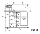
他のマルチビット配置を図11に示し、それは、各行に対する複数のアドレスライン14及び各列に対する単一列ライン16を有する。選択ライン76を各行に設けて、列ライン16をデータライン77を通じてTFT12に接続する選択トランジスタ74を制御する。
Another multi-bit arrangement is shown in FIG. 11, which has
使用の際には、複数のアドレスライン14のうちの一つがイネーブルされて、対応するデータ記憶キャパシタ70が選択される。読出しライン52をイネーブルして、列ライン16上の選択されたデータ記憶キャパシタ70のデータを読出し回路51が読み出せるようにしてもよい。選択ライン76が選択TFT74をイネーブルして、選択されたデータ記憶キャパシタ70に列ライン16のデータを書き込むこともできる。
In use, one of the plurality of
データ記憶キャパシタ70に接続した読出し回路51の一例を、図12に示す。データ記憶キャパシタ70は、読出しTFT82を通じて列16に直列接続した第1TFT80を制御する。読出しTFT82は読出しライン52によって制御される。リードライン52が読出しTFT82をスイッチオンすると、データ記憶キャパシタ70に記憶されたデータが列16で読み出される。
An example of the read
既に説明したように回路72を駆動するためにデータ記憶キャパシタ70の並列接続とともに、複数のデータ記憶キャパシタ70のデータを、図13に図示したような単一データライン84によって駆動回路72に接続することができる。この回路において、個別のTFT12を次々とアドレス指定して対応するデータ記憶キャパシタ70を駆動回路72に接続することによって、データを駆動回路72に転送する。
As already described, the
他の実施の形態を図14に示し、それは、画素キャパシタンス18それ自体を用いて順次電荷再分布デジタル−アナログ変換を行う。この回路の特徴は、米国特許第5448258号及び米国特許第5923311号に詳細に記載されており、参照することによってここに組み込まれる。現在の目的のために、図13に示すように、キャパシタ70を、各スイッチ12を通じてデータライン84に接続し、データライン84は画素キャパシタンス18を駆動する。
Another embodiment is shown in FIG. 14, which performs sequential charge redistribution digital-to-analog conversion using the
静止モードにおいて画素内に格納されたデータを用いるとともにそれ以外において外部信号源から供給されたデータを用いて、アレイ中の一部の画素を同時に操作することができる。これを、適切な信号を用いてディスプレイを分割するだけで画素回路を変形することなく行うことができる。このアプローチは、電力消費を最小にすることができる。 Some data in the array can be manipulated simultaneously using data stored in the pixels in static mode and otherwise using data supplied from an external signal source. This can be done without changing the pixel circuit simply by dividing the display using an appropriate signal. This approach can minimize power consumption.
例えば、表示の一部が動画を示し、表示の残りが静止背景を示す。外部ビデオ源は、動画を示す画像の領域のデータをディスプレイに供給するだけでよく、これによって電力をセーブする。 For example, a part of the display shows a moving image, and the rest of the display shows a still background. The external video source only needs to supply data to the display in the area of the image showing the moving image, thereby saving power.
本発明は、種々のアクティブマトリックス表示装置に適用可能であり、既に説明したのと同様な画素回路を、AMLCD及びAMLED以外の表示装置に用いることができ、この場合、例えばエレクトロクロミック(electrochromic)タイプ、エレクトロホレテック(electrophoretic)タイプ及びエレクトロルミネセンt(electroluminescent)タイプの表示装置において静止画像を記憶するのが望ましい。アクティブマトリックスLEDの一例は、欧州特許公開番号第115205号に記載されており、その内容を、バックグランド材料としてここに組み込む。 The present invention can be applied to various active matrix display devices, and a pixel circuit similar to that described above can be used for display devices other than AMLCD and AMLED. In this case, for example, an electrochromic type It is desirable to store still images in display devices of the electrophoretic type and the electroluminescent type. An example of an active matrix LED is described in European Patent Publication No. 115205, the contents of which are incorporated herein as background material.
本発明は、上記実施の形態に限定されるものではなく、幾多の変更及び変形が可能である。 The present invention is not limited to the above-described embodiment, and many changes and modifications can be made.
Claims (7)
前記複数の画素の各々が、画像データ記憶キャパシタンスと、
前記列電極と前記画像データ記憶キャパシタンスとの間に接続され、前記画像データ記憶キャパシタンスの電圧を一旦取り込み、前記取り込んだ画像データ記憶キャパシタンスの状態に基づいて前記列電極を荷電するバッファとして機能する読出し回路と、を有することを特徴とするアクティブマトリックス表示装置。A plurality of pixels arranged in a matrix and a column electrode extending along a column of corresponding pixels;
Each of the plurality of pixels, and images data storage capacitance,
Buffer which is connected between the column electrode and the front Kiga image data storage capacitor down scan, the image data storage capacitance voltage once uptake of, charged the column electrodes based on the state of the captured image data storage capacitance An active matrix display device , comprising: a readout circuit that functions as:
前記複数の画素の各々が、対応する行電極によって選択されたときに対応する列電極を前記データ記憶キャパシタンスに接続するスイッチを有し、
前記読み出し回路が、前記画像データ記憶キャパシタンスの電圧を前記対応する列電極に読み出すために対応する読出しラインによって制御されることを特徴とするアクティブマトリックス表示装置。An active matrix display device according to claim 1 Symbol placement and a read line extending along the row electrodes, the row of the corresponding pixel,
Each of the plurality of pixels comprises a switch that connects a corresponding column electrode to the data storage capacitance when selected by a corresponding row electrode;
The readout circuit, wherein the image data storing active matrix display device comprising that you are controlled by a read line voltage capacitance corresponding to read in the corresponding column electrodes.
前記複数の画素の各々が、画像データ記憶キャパシタンスと、Each of the plurality of pixels includes an image data storage capacitance;
対応する行電極によって選択されたときに対応する列電極を前記データ記憶キャパシタンスに接続する第1スイッチと、A first switch connecting a corresponding column electrode to the data storage capacitance when selected by a corresponding row electrode;
前記画像データ記憶キャパシタンスに接続された入力部を有し、画素表示素子を駆動する駆動回路と、A drive circuit having an input connected to the image data storage capacitance and driving a pixel display element;
前記列電極と前記駆動回路の出力部との間に配置され、前記画像データ記憶キャパシタンスの電圧に基づいて前記列電極を荷電するために対応する読出しラインによって制御され、前記対応する読出しラインの制御の下で前記駆動回路の出力部を前記対応する列電極に接続する第2スイッチとを有することを特徴とするアクティブマトリックス表示装置。Controlled by the corresponding readout line, arranged between the column electrode and the output of the drive circuit, controlled by the corresponding readout line to charge the column electrode based on the voltage of the image data storage capacitance And a second switch for connecting the output of the drive circuit to the corresponding column electrode.
前記複数の画素の各々が、複数の画像データ記憶キャパシタンスと、Each of the plurality of pixels includes a plurality of image data storage capacitances;
データラインと、Data lines,
対応する行電極によって選択されたときに対応する画像データ記憶キャパシタンスを前記データラインに接続する複数の第3スイッチと、A plurality of third switches for connecting a corresponding image data storage capacitance to the data line when selected by a corresponding row electrode;
前記列電極と前記データラインとの間に接続され、前記複数の行電極の1つによって選択された前記画像データ記憶キャパシタンスの電圧を一旦取り込み、前記取り込んだ画像データ記憶キャパシタンスの電圧に基づいて前記列電極を荷電するバッファとして機能する読出し回路と、The voltage of the image data storage capacitance connected between the column electrode and the data line and selected by one of the plurality of row electrodes is temporarily captured, and the voltage is stored based on the captured voltage of the image data storage capacitance. A readout circuit that functions as a buffer for charging the column electrodes;
前記列電極上の電圧を前記複数の行電極の1つによって選択された前記画像データ記憶キャパシタンスに書き込むように、前記選択ラインの制御の下で前記列電極を前記データラインを介して前記第3スイッチに接続する第4スイッチと、The column electrode is connected via the data line to the third line under control of the selection line to write a voltage on the column electrode to the image data storage capacitance selected by one of the plurality of row electrodes. A fourth switch connected to the switch;
を有し、Have
前記読み出し回路が、前記読出しラインの制御の下で前記データライン上にある前記複数の行電極の1つによって選択された前記画像データキャパシタンスの電圧を前記対応する列電極に読み出すことを特徴とするアクティブマトリックス表示装置。The readout circuit reads out the voltage of the image data capacitance selected by one of the plurality of row electrodes on the data line to the corresponding column electrode under the control of the readout line. Active matrix display device.
Applications Claiming Priority (5)
| Application Number | Priority Date | Filing Date | Title |
|---|---|---|---|
| GB0117226.1 | 2001-07-14 | ||
| GBGB0117226.1A GB0117226D0 (en) | 2001-07-14 | 2001-07-14 | Active matrix display devices |
| GB0125969.6 | 2001-10-30 | ||
| GBGB0125969.6A GB0125969D0 (en) | 2001-07-14 | 2001-10-30 | Active matrix display devices |
| PCT/IB2002/002993 WO2003009268A2 (en) | 2001-07-14 | 2002-07-12 | Active matrix display devices |
Publications (3)
| Publication Number | Publication Date |
|---|---|
| JP2004536347A JP2004536347A (en) | 2004-12-02 |
| JP2004536347A5 JP2004536347A5 (en) | 2011-06-02 |
| JP4914558B2 true JP4914558B2 (en) | 2012-04-11 |
Family
ID=9918520
Family Applications (1)
| Application Number | Title | Priority Date | Filing Date |
|---|---|---|---|
| JP2003514534A Expired - Fee Related JP4914558B2 (en) | 2001-07-14 | 2002-07-12 | Active matrix display device |
Country Status (3)
| Country | Link |
|---|---|
| JP (1) | JP4914558B2 (en) |
| KR (1) | KR100888461B1 (en) |
| GB (2) | GB0117226D0 (en) |
Families Citing this family (8)
| Publication number | Priority date | Publication date | Assignee | Title |
|---|---|---|---|---|
| KR100613091B1 (en) * | 2004-12-24 | 2006-08-16 | 삼성에스디아이 주식회사 | Data Integrated Circuit and Driving Method of Light Emitting Display Using The Same |
| US7952546B2 (en) * | 2007-06-27 | 2011-05-31 | Chimei Innolux Corporation | Sample/hold circuit, electronic system, and control method utilizing the same |
| JP5125378B2 (en) * | 2007-10-03 | 2013-01-23 | セイコーエプソン株式会社 | Control method, control device, display body, and information display device |
| JP5011514B2 (en) * | 2009-03-19 | 2012-08-29 | 奇美電子股▲ふん▼有限公司 | Method for driving liquid crystal display device and liquid crystal display device |
| JP5386409B2 (en) * | 2010-03-08 | 2014-01-15 | 群創光電股▲ふん▼有限公司 | Active matrix display device and electronic apparatus having the same |
| KR101917837B1 (en) * | 2011-11-10 | 2018-11-14 | 엘지디스플레이 주식회사 | Liquid crystal display apparatus and method for driving the same |
| WO2013105393A1 (en) * | 2012-01-12 | 2013-07-18 | シャープ株式会社 | Pixel circuit and display device |
| KR102378589B1 (en) | 2015-08-21 | 2022-03-28 | 삼성디스플레이 주식회사 | Demultiplexer, display device including the same and driving method thereof |
Family Cites Families (4)
| Publication number | Priority date | Publication date | Assignee | Title |
|---|---|---|---|---|
| JPS5799688A (en) * | 1980-12-11 | 1982-06-21 | Sharp Kk | Display driving circuit |
| JPS59208590A (en) * | 1983-05-11 | 1984-11-26 | シャープ株式会社 | Driving circuit for display |
| JP3102666B2 (en) * | 1993-06-28 | 2000-10-23 | シャープ株式会社 | Image display device |
| JP3832086B2 (en) * | 1998-04-15 | 2006-10-11 | セイコーエプソン株式会社 | Reflective liquid crystal device and reflective projector |
-
2001
- 2001-07-14 GB GBGB0117226.1A patent/GB0117226D0/en not_active Ceased
- 2001-10-30 GB GBGB0125969.6A patent/GB0125969D0/en not_active Ceased
-
2002
- 2002-07-12 KR KR1020037003629A patent/KR100888461B1/en not_active IP Right Cessation
- 2002-07-12 JP JP2003514534A patent/JP4914558B2/en not_active Expired - Fee Related
Also Published As
| Publication number | Publication date |
|---|---|
| KR100888461B1 (en) | 2009-03-11 |
| KR20040023563A (en) | 2004-03-18 |
| GB0117226D0 (en) | 2001-09-05 |
| JP2004536347A (en) | 2004-12-02 |
| GB0125969D0 (en) | 2001-12-19 |
Similar Documents
| Publication | Publication Date | Title |
|---|---|---|
| US6897843B2 (en) | Active matrix display devices | |
| US7230597B2 (en) | Active matrix array devices | |
| KR100417572B1 (en) | Display device | |
| US7586473B2 (en) | Active matrix array device, electronic device and operating method for an active matrix array device | |
| KR101037554B1 (en) | Active matrix display device and driving method of the same | |
| US20020063671A1 (en) | Active matrix liquid crystal display devices | |
| US7545355B2 (en) | Image display apparatus and driving method thereof | |
| KR100726052B1 (en) | Electrooptic device and method for driving thereof, digitally-driven liquid crystal display, electronic apparatus, and projector | |
| US9208714B2 (en) | Display panel for refreshing image data and operating method thereof | |
| US11043163B2 (en) | Display device and electronic shelf label | |
| KR100465472B1 (en) | Active metrix type display device | |
| JP4914558B2 (en) | Active matrix display device | |
| US10559286B2 (en) | Display device | |
| US8791895B2 (en) | Liquid crystal display device and drive method therefor | |
| US8339351B2 (en) | Display device | |
| US8736591B2 (en) | Display device using pixel memory circuit to reduce flicker with reduced power consumption | |
| JP2004536347A5 (en) | ||
| WO2020066176A1 (en) | Display device and digital signage | |
| KR100879769B1 (en) | Active matrix array devices | |
| JP2020052219A (en) | Display and electronic signboard | |
| JP2020042191A (en) | Display and electronic signboard |
Legal Events
| Date | Code | Title | Description |
|---|---|---|---|
| A621 | Written request for application examination |
Free format text: JAPANESE INTERMEDIATE CODE: A621 Effective date: 20050711 |
|
| A711 | Notification of change in applicant |
Free format text: JAPANESE INTERMEDIATE CODE: A711 Effective date: 20070202 |
|
| A131 | Notification of reasons for refusal |
Free format text: JAPANESE INTERMEDIATE CODE: A131 Effective date: 20080722 |
|
| A521 | Request for written amendment filed |
Free format text: JAPANESE INTERMEDIATE CODE: A523 Effective date: 20081022 |
|
| A02 | Decision of refusal |
Free format text: JAPANESE INTERMEDIATE CODE: A02 Effective date: 20081202 |
|
| A521 | Request for written amendment filed |
Free format text: JAPANESE INTERMEDIATE CODE: A523 Effective date: 20090401 |
|
| A911 | Transfer to examiner for re-examination before appeal (zenchi) |
Free format text: JAPANESE INTERMEDIATE CODE: A911 Effective date: 20090407 |
|
| A912 | Re-examination (zenchi) completed and case transferred to appeal board |
Free format text: JAPANESE INTERMEDIATE CODE: A912 Effective date: 20091204 |
|
| A601 | Written request for extension of time |
Free format text: JAPANESE INTERMEDIATE CODE: A601 Effective date: 20100720 |
|
| A602 | Written permission of extension of time |
Free format text: JAPANESE INTERMEDIATE CODE: A602 Effective date: 20100726 |
|
| A601 | Written request for extension of time |
Free format text: JAPANESE INTERMEDIATE CODE: A601 Effective date: 20100820 |
|
| A602 | Written permission of extension of time |
Free format text: JAPANESE INTERMEDIATE CODE: A602 Effective date: 20100827 |
|
| A601 | Written request for extension of time |
Free format text: JAPANESE INTERMEDIATE CODE: A601 Effective date: 20110216 |
|
| A602 | Written permission of extension of time |
Free format text: JAPANESE INTERMEDIATE CODE: A602 Effective date: 20110222 |
|
| A601 | Written request for extension of time |
Free format text: JAPANESE INTERMEDIATE CODE: A601 Effective date: 20110316 |
|
| A602 | Written permission of extension of time |
Free format text: JAPANESE INTERMEDIATE CODE: A602 Effective date: 20110322 |
|
| A524 | Written submission of copy of amendment under article 19 pct |
Free format text: JAPANESE INTERMEDIATE CODE: A524 Effective date: 20110418 |
|
| A521 | Request for written amendment filed |
Free format text: JAPANESE INTERMEDIATE CODE: A523 Effective date: 20111130 |
|
| A01 | Written decision to grant a patent or to grant a registration (utility model) |
Free format text: JAPANESE INTERMEDIATE CODE: A01 |
|
| A61 | First payment of annual fees (during grant procedure) |
Free format text: JAPANESE INTERMEDIATE CODE: A61 Effective date: 20120123 |
|
| R150 | Certificate of patent or registration of utility model |
Free format text: JAPANESE INTERMEDIATE CODE: R150 |
|
| FPAY | Renewal fee payment (event date is renewal date of database) |
Free format text: PAYMENT UNTIL: 20150127 Year of fee payment: 3 |
|
| R250 | Receipt of annual fees |
Free format text: JAPANESE INTERMEDIATE CODE: R250 |
|
| LAPS | Cancellation because of no payment of annual fees |