JP2016127232A - ウェーハの加工方法 - Google Patents
ウェーハの加工方法 Download PDFInfo
- Publication number
- JP2016127232A JP2016127232A JP2015002218A JP2015002218A JP2016127232A JP 2016127232 A JP2016127232 A JP 2016127232A JP 2015002218 A JP2015002218 A JP 2015002218A JP 2015002218 A JP2015002218 A JP 2015002218A JP 2016127232 A JP2016127232 A JP 2016127232A
- Authority
- JP
- Japan
- Prior art keywords
- wafer
- outer peripheral
- cutting
- protection tape
- surface protection
- Prior art date
- Legal status (The legal status is an assumption and is not a legal conclusion. Google has not performed a legal analysis and makes no representation as to the accuracy of the status listed.)
- Pending
Links
Images


Classifications
-
- H—ELECTRICITY
- H10—SEMICONDUCTOR DEVICES; ELECTRIC SOLID-STATE DEVICES NOT OTHERWISE PROVIDED FOR
- H10P—GENERIC PROCESSES OR APPARATUS FOR THE MANUFACTURE OR TREATMENT OF DEVICES COVERED BY CLASS H10
- H10P54/00—Cutting or separating of wafers, substrates or parts of devices
-
- H—ELECTRICITY
- H10—SEMICONDUCTOR DEVICES; ELECTRIC SOLID-STATE DEVICES NOT OTHERWISE PROVIDED FOR
- H10P—GENERIC PROCESSES OR APPARATUS FOR THE MANUFACTURE OR TREATMENT OF DEVICES COVERED BY CLASS H10
- H10P72/00—Handling or holding of wafers, substrates or devices during manufacture or treatment thereof
- H10P72/70—Handling or holding of wafers, substrates or devices during manufacture or treatment thereof for supporting or gripping
- H10P72/74—Handling or holding of wafers, substrates or devices during manufacture or treatment thereof for supporting or gripping using temporarily an auxiliary support
- H10P72/7402—Wafer tapes, e.g. grinding or dicing support tapes
-
- H—ELECTRICITY
- H10—SEMICONDUCTOR DEVICES; ELECTRIC SOLID-STATE DEVICES NOT OTHERWISE PROVIDED FOR
- H10P—GENERIC PROCESSES OR APPARATUS FOR THE MANUFACTURE OR TREATMENT OF DEVICES COVERED BY CLASS H10
- H10P72/00—Handling or holding of wafers, substrates or devices during manufacture or treatment thereof
- H10P72/70—Handling or holding of wafers, substrates or devices during manufacture or treatment thereof for supporting or gripping
- H10P72/74—Handling or holding of wafers, substrates or devices during manufacture or treatment thereof for supporting or gripping using temporarily an auxiliary support
- H10P72/7412—Handling or holding of wafers, substrates or devices during manufacture or treatment thereof for supporting or gripping using temporarily an auxiliary support the auxiliary support including means facilitating the separation of a device or wafer from the auxiliary support
-
- H—ELECTRICITY
- H10—SEMICONDUCTOR DEVICES; ELECTRIC SOLID-STATE DEVICES NOT OTHERWISE PROVIDED FOR
- H10P—GENERIC PROCESSES OR APPARATUS FOR THE MANUFACTURE OR TREATMENT OF DEVICES COVERED BY CLASS H10
- H10P72/00—Handling or holding of wafers, substrates or devices during manufacture or treatment thereof
- H10P72/70—Handling or holding of wafers, substrates or devices during manufacture or treatment thereof for supporting or gripping
- H10P72/74—Handling or holding of wafers, substrates or devices during manufacture or treatment thereof for supporting or gripping using temporarily an auxiliary support
- H10P72/7416—Handling or holding of wafers, substrates or devices during manufacture or treatment thereof for supporting or gripping using temporarily an auxiliary support used during dicing or grinding
-
- H—ELECTRICITY
- H10—SEMICONDUCTOR DEVICES; ELECTRIC SOLID-STATE DEVICES NOT OTHERWISE PROVIDED FOR
- H10P—GENERIC PROCESSES OR APPARATUS FOR THE MANUFACTURE OR TREATMENT OF DEVICES COVERED BY CLASS H10
- H10P72/00—Handling or holding of wafers, substrates or devices during manufacture or treatment thereof
- H10P72/70—Handling or holding of wafers, substrates or devices during manufacture or treatment thereof for supporting or gripping
- H10P72/74—Handling or holding of wafers, substrates or devices during manufacture or treatment thereof for supporting or gripping using temporarily an auxiliary support
- H10P72/7422—Handling or holding of wafers, substrates or devices during manufacture or treatment thereof for supporting or gripping using temporarily an auxiliary support used to protect an active side of a device or wafer
Landscapes
- Mechanical Treatment Of Semiconductor (AREA)
Abstract
【解決手段】本発明のウェーハの加工方法は、外周余剰領域6においてのみ接着層11を介して表面保護テープ10を貼着するテープ貼着工程と、ウェーハ1の外周部7を回転する切削ブレード13により切削し、所定幅及び所定深さを有する外周切削部8を形成する切削工程とを有するため、切削時に生じるパーティクルをデバイス領域5に付着させることなく、容易に外周部7をエッジトリミングできる。また、支持基板をウェーハ1に貼り合わせてエッジトリミングした場合と比べて、切削ブレード13で切削する部分の体積が小さくなるため、切削ブレード13の加工速度を高く設定できウェーハ1の加工品質が向上する。さらには、切削後のウェーハ1のデバイス領域5に接着層が残ることがないため、デバイス領域5の洗浄が不要となる。
【選択図】図3
Description
切削工程を実施する際には、例えば支持基板をウェーハに貼り合わせて切削する場合と比べて、切削する部分の体積が小さくなるため、切削ブレードの加工速度を上げてもウェーハに加えられるダメージが少なくて済み、高い加工品質を得ることができる。また、切削工程後のウェーハから表面保護テープを剥離する際には、デバイス領域に接着層が残らないため、切削工程後におけるデバイス領域の洗浄が不要となる。
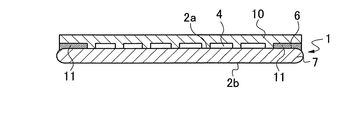
図1に示すウェーハ1は、被加工物の一例であって、例えば円板状のシリコン基板により構成されている。ウェーハ1の表面2aには、格子状の分割予定ライン3によって区画されたそれぞれの領域にデバイス4が形成されたデバイス領域5と、デバイス領域5を取り囲む外周余剰領域6とが形成されている。
図2に示すように、ウェーハ1の表面2aに形成されたデバイス4を保護する表面保護テープ10を、ウェーハ1の表面2aに貼着する。表面保護テープ10は、ウェーハ1の表面2aの全面を覆う面積を有している。表面保護テープ10には、図1に示したウェーハ1の外周余剰領域6に接触する周縁部分にのみ接着層11が形成されており、接着層11は、例えばシリコンなどからなる基板に対して接着力を有する糊で構成されている。一方、表面保護テープ10のデバイス4に接触する面には、接着層は形成されていない。
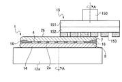
表面保護テープ貼着工程を実施した後、図3に示すように、回転可能な切削ブレード13によってウェーハ1の外周部7に対してエッジトリミングを行う。なお、使用する切削ブレード13としては、ブレードの刃先がフラットな形状で構成されたタイプのものが好適である。
切削工程を実施した後、図5に示すように、被加工物を研削する研削手段15によってウェーハ1を所望の仕上げ厚みに研削する。研削手段15は、鉛直方向の軸心を有するスピンドル150と、スピンドル150の下端においてマウント151を介して装着された研削ホイール152と、研削ホイール152の下部において環状に固着された研削砥石153とを少なくとも備えている。
切削ブレード13でウェーハ1の表面保護テープ10ごと外周部7に対してエッジトリミングする切削工程を実施するため、ウェーハ1に対する表面保護テープ10の貼着状態を安定させたまま、切削時に生じるパーティクルをデバイス領域5に付着させることなく、容易に外周部7をエッジトリミングすることができる。
また、従来のように支持基板をウェーハ1に貼り合わせてエッジトリミングした場合と比べて、切削ブレード13で切削する部分の体積が小さくなるため、切削ブレード13の加工速度を高くすることができる。
また、表面保護テープ貼着工程では外周余剰領域においてのみ接着層を介して表面保護テープを貼着し、表面保護テープ10とデバイス領域5との間に接着層が介在しないため、切削後のウェーハ1の表面2aから表面保護テープ10を剥離してもデバイス領域5に接着層が残ることがなく、デバイス領域5の洗浄が不要となる。
次に、図6に示すウェーハ1の外周部7に対してエッジトリミングを行い、ウェーハ1を所望の仕上げ厚みに薄化する加工方法の第2例について説明する。なお、ウェーハの加工方法の第2例では、図1に示した外周余剰領域6のうち、デバイス領域5の近傍に位置する部分を第1の外周余剰領域6a,第1の外周余剰領域6aよりも径方向外側にありエッジトリミングが施される部分を第2の外周余剰領域6bとして説明する。
図6に示すように、ウェーハ1の表面2aにウェーハ1よりも小径の表面保護テープ20を貼着する。表面保護テープ20は、少なくとも図1に示したデバイス領域5を覆う大きさを有している。また、表面保護テープ20には、第1の外周余剰領域6aに接触する周縁部分にのみ接着層21が形成されている。
表面保護テープ貼着工程を実施した後、図7に示すように、ウェーハ1の外周縁において露出した最外周部7aを切削ブレード13によって切削する。ウェーハの加工方法の第1例と同様に、保持テーブル12でウェーハ1を吸引保持したら、保持テーブル12を切削ブレード13の下方に移動させる。続いて切削ブレード13を例えば矢印B方向に回転させながら、切削ブレード13をウェーハ1の表面2aに接近する方向に下降させ、切削ブレード13の刃先をウェーハ1の最外周部7aに直接切り込ませる。
5:デバイス領域 6:外周余剰領域 6a:第1の外周余剰領域
6b:第2の外周余剰領域 7:外周部 7a:最外周部 8,9:外周切削部
10:表面保護テープ 11:接着層
12,12a:保持テーブル 13:切削ブレード 14:支持基板
15:研削手段 150:スピンドル 151:マウント 152:研削ホイール
153:研削砥石
16:接着剤
20:表面保護テープ 21:接着層
Claims (3)
- 表面に複数のデバイスが形成されたデバイス領域と前記デバイス領域を取り囲む外周余剰領域とが形成された被加工物の加工方法であって、
前記外周余剰領域においてのみ接着層を介して表面保護テープを貼着する表面保護テープ貼着工程と、
回転する切削ブレードにより被加工物の表面の外周部を切削し、所定幅及び所定深さを有する外周切削部を形成する切削工程と、を有するウェーハの加工方法。 - 前記表面保護テープは、ウェーハの表面の全面を覆う面積を有し、
前記切削工程では、前記表面保護テープを切削するとともにウェーハの外周部を切削する請求項1に記載のウェーハの加工方法。 - 前記表面保護テープは、少なくとも前記デバイス領域を覆う大きさを有し、
前記表面保護テープ貼着工程では、前記表面保護テープをウェーハの表面に貼着することによってウェーハの最外周部を全周にわたって露出させ、
前記切削工程では、露出されたウェーハの最外周部を切削する請求項1に記載のウェーハの加工方法。
Priority Applications (6)
| Application Number | Priority Date | Filing Date | Title |
|---|---|---|---|
| JP2015002218A JP2016127232A (ja) | 2015-01-08 | 2015-01-08 | ウェーハの加工方法 |
| TW104141528A TWI686854B (zh) | 2015-01-08 | 2015-12-10 | 晶圓的加工方法 |
| CN201511020218.4A CN105789126A (zh) | 2015-01-08 | 2015-12-30 | 晶片的加工方法 |
| KR1020160000529A KR20160085704A (ko) | 2015-01-08 | 2016-01-04 | 웨이퍼의 가공 방법 |
| US14/988,438 US9595463B2 (en) | 2015-01-08 | 2016-01-05 | Wafer processing method |
| DE102016200023.3A DE102016200023B4 (de) | 2015-01-08 | 2016-01-05 | Waferbearbeitungsverfahren |
Applications Claiming Priority (1)
| Application Number | Priority Date | Filing Date | Title |
|---|---|---|---|
| JP2015002218A JP2016127232A (ja) | 2015-01-08 | 2015-01-08 | ウェーハの加工方法 |
Publications (1)
| Publication Number | Publication Date |
|---|---|
| JP2016127232A true JP2016127232A (ja) | 2016-07-11 |
Family
ID=56233462
Family Applications (1)
| Application Number | Title | Priority Date | Filing Date |
|---|---|---|---|
| JP2015002218A Pending JP2016127232A (ja) | 2015-01-08 | 2015-01-08 | ウェーハの加工方法 |
Country Status (6)
| Country | Link |
|---|---|
| US (1) | US9595463B2 (ja) |
| JP (1) | JP2016127232A (ja) |
| KR (1) | KR20160085704A (ja) |
| CN (1) | CN105789126A (ja) |
| DE (1) | DE102016200023B4 (ja) |
| TW (1) | TWI686854B (ja) |
Cited By (3)
| Publication number | Priority date | Publication date | Assignee | Title |
|---|---|---|---|---|
| JP2019021884A (ja) * | 2017-07-21 | 2019-02-07 | 株式会社ディスコ | ウェーハの加工方法 |
| JP2019520708A (ja) * | 2016-06-28 | 2019-07-18 | 株式会社ディスコ | ウェハを処理する方法 |
| JP2020035918A (ja) * | 2018-08-30 | 2020-03-05 | 株式会社ディスコ | 被加工物の加工方法 |
Families Citing this family (9)
| Publication number | Priority date | Publication date | Assignee | Title |
|---|---|---|---|---|
| JP2018092963A (ja) * | 2016-11-30 | 2018-06-14 | 株式会社ディスコ | ウェーハの加工方法 |
| US10861761B2 (en) * | 2017-09-29 | 2020-12-08 | Taiwan Semiconductor Manufacturing Company Ltd. | Semiconductor packaged wafer and method for forming the same |
| WO2019124031A1 (ja) * | 2017-12-19 | 2019-06-27 | 東京エレクトロン株式会社 | 基板処理システム、基板処理方法及びコンピュータ記憶媒体 |
| JP6991673B2 (ja) | 2018-02-27 | 2022-01-12 | 株式会社ディスコ | 剥離方法 |
| JP7187112B2 (ja) * | 2018-08-13 | 2022-12-12 | 株式会社ディスコ | キャリア板の除去方法 |
| JP7222636B2 (ja) * | 2018-09-12 | 2023-02-15 | 株式会社ディスコ | エッジトリミング装置 |
| CN109461647A (zh) * | 2018-11-16 | 2019-03-12 | 德淮半导体有限公司 | 半导体装置的制造方法 |
| JP7187115B2 (ja) * | 2018-12-04 | 2022-12-12 | 株式会社ディスコ | ウェーハの加工方法 |
| CN110060957B (zh) * | 2019-04-22 | 2020-07-31 | 长江存储科技有限责任公司 | 半导体结构及半导体工艺方法 |
Citations (7)
| Publication number | Priority date | Publication date | Assignee | Title |
|---|---|---|---|---|
| JP2004207459A (ja) * | 2002-12-25 | 2004-07-22 | Disco Abrasive Syst Ltd | 半導体ウェーハの研削方法 |
| JP2005005447A (ja) * | 2003-06-11 | 2005-01-06 | Sharp Corp | 半導体基板の製造方法 |
| JP2007042811A (ja) * | 2005-08-02 | 2007-02-15 | Tokyo Seimitsu Co Ltd | ウェーハ外周研削方法及びウェーハ外周研削装置 |
| US20100248414A1 (en) * | 2009-03-31 | 2010-09-30 | Taiwan Semiconductor Manufacturing Company, Ltd. | Method of wafer bonding |
| JP2011124266A (ja) * | 2009-12-08 | 2011-06-23 | Disco Abrasive Syst Ltd | ウエーハの加工方法 |
| JP2012231057A (ja) * | 2011-04-27 | 2012-11-22 | Disco Abrasive Syst Ltd | ウエーハの加工方法 |
| JP2013247135A (ja) * | 2012-05-23 | 2013-12-09 | Disco Abrasive Syst Ltd | ウエーハの加工方法 |
Family Cites Families (10)
| Publication number | Priority date | Publication date | Assignee | Title |
|---|---|---|---|---|
| KR100249313B1 (ko) * | 1997-07-25 | 2000-03-15 | 윤종용 | 반도체 웨이퍼 테이프 라미네이팅시스템 및 이를 이용한 라미네이팅방법 |
| KR100259015B1 (ko) * | 1998-01-17 | 2000-06-15 | 윤종용 | 복수개의 테이프 절단기를 포함하는 테이프 부착 장치의테이프 절단부 |
| JP4347960B2 (ja) * | 1999-09-14 | 2009-10-21 | 株式会社ディスコ | ダイシング方法 |
| JP3768069B2 (ja) * | 2000-05-16 | 2006-04-19 | 信越半導体株式会社 | 半導体ウエーハの薄型化方法 |
| JP4774286B2 (ja) | 2005-12-08 | 2011-09-14 | 株式会社ディスコ | 基板の切削加工方法 |
| JP2007281051A (ja) * | 2006-04-04 | 2007-10-25 | Miraial Kk | 半導体ウエハのチップ加工方法 |
| JP5500942B2 (ja) * | 2009-10-28 | 2014-05-21 | 株式会社ディスコ | ウエーハの加工方法 |
| JP2013008915A (ja) * | 2011-06-27 | 2013-01-10 | Toshiba Corp | 基板加工方法及び基板加工装置 |
| JP5840003B2 (ja) * | 2012-01-23 | 2016-01-06 | 株式会社ディスコ | ウエーハの加工方法 |
| JP2015217461A (ja) | 2014-05-16 | 2015-12-07 | 株式会社ディスコ | ウェーハの加工方法 |
-
2015
- 2015-01-08 JP JP2015002218A patent/JP2016127232A/ja active Pending
- 2015-12-10 TW TW104141528A patent/TWI686854B/zh active
- 2015-12-30 CN CN201511020218.4A patent/CN105789126A/zh active Pending
-
2016
- 2016-01-04 KR KR1020160000529A patent/KR20160085704A/ko not_active Ceased
- 2016-01-05 DE DE102016200023.3A patent/DE102016200023B4/de active Active
- 2016-01-05 US US14/988,438 patent/US9595463B2/en active Active
Patent Citations (7)
| Publication number | Priority date | Publication date | Assignee | Title |
|---|---|---|---|---|
| JP2004207459A (ja) * | 2002-12-25 | 2004-07-22 | Disco Abrasive Syst Ltd | 半導体ウェーハの研削方法 |
| JP2005005447A (ja) * | 2003-06-11 | 2005-01-06 | Sharp Corp | 半導体基板の製造方法 |
| JP2007042811A (ja) * | 2005-08-02 | 2007-02-15 | Tokyo Seimitsu Co Ltd | ウェーハ外周研削方法及びウェーハ外周研削装置 |
| US20100248414A1 (en) * | 2009-03-31 | 2010-09-30 | Taiwan Semiconductor Manufacturing Company, Ltd. | Method of wafer bonding |
| JP2011124266A (ja) * | 2009-12-08 | 2011-06-23 | Disco Abrasive Syst Ltd | ウエーハの加工方法 |
| JP2012231057A (ja) * | 2011-04-27 | 2012-11-22 | Disco Abrasive Syst Ltd | ウエーハの加工方法 |
| JP2013247135A (ja) * | 2012-05-23 | 2013-12-09 | Disco Abrasive Syst Ltd | ウエーハの加工方法 |
Cited By (3)
| Publication number | Priority date | Publication date | Assignee | Title |
|---|---|---|---|---|
| JP2019520708A (ja) * | 2016-06-28 | 2019-07-18 | 株式会社ディスコ | ウェハを処理する方法 |
| JP2019021884A (ja) * | 2017-07-21 | 2019-02-07 | 株式会社ディスコ | ウェーハの加工方法 |
| JP2020035918A (ja) * | 2018-08-30 | 2020-03-05 | 株式会社ディスコ | 被加工物の加工方法 |
Also Published As
| Publication number | Publication date |
|---|---|
| TWI686854B (zh) | 2020-03-01 |
| KR20160085704A (ko) | 2016-07-18 |
| TW201633393A (zh) | 2016-09-16 |
| US20160204016A1 (en) | 2016-07-14 |
| US9595463B2 (en) | 2017-03-14 |
| DE102016200023B4 (de) | 2025-10-09 |
| CN105789126A (zh) | 2016-07-20 |
| DE102016200023A1 (de) | 2016-07-14 |
Similar Documents
| Publication | Publication Date | Title |
|---|---|---|
| JP2016127232A (ja) | ウェーハの加工方法 | |
| KR102024390B1 (ko) | 표면 보호 부재 및 가공 방법 | |
| US20150332911A1 (en) | Method of processing wafer | |
| JP2013008915A (ja) | 基板加工方法及び基板加工装置 | |
| JP2017204555A (ja) | 切削方法 | |
| TWI759491B (zh) | 晶圓加工方法 | |
| KR20210075049A (ko) | 웨이퍼 가공 방법 및 중간 부재 | |
| JP2013247135A (ja) | ウエーハの加工方法 | |
| JP2016127098A (ja) | ウェーハの加工方法 | |
| JP7657034B2 (ja) | ウェーハの加工方法 | |
| TW201822267A (zh) | 晶圓的加工方法 | |
| JP5977633B2 (ja) | 加工方法 | |
| JP2016051779A (ja) | ウエーハの貼り合わせ方法及び貼り合わせワークの剥離方法 | |
| TWI804670B (zh) | 半導體裝置的製造方法和製造裝置 | |
| KR102535551B1 (ko) | 피가공물의 연삭 방법 | |
| JP2018148135A (ja) | リチウムタンタレートウェーハの加工方法 | |
| JP5912310B2 (ja) | ウェーハの加工方法 | |
| JP2012222310A (ja) | ウェーハの加工方法 | |
| JP2016219757A (ja) | 被加工物の分割方法 | |
| JP2015149386A (ja) | ウェーハの加工方法 | |
| JP6049170B2 (ja) | 研削方法 | |
| JP2013102080A (ja) | ウエーハの支持基板およびウエーハの加工方法 | |
| JP6955977B2 (ja) | チップの形成方法 | |
| JP2024066612A (ja) | ウエーハの加工方法 | |
| JP2014041885A (ja) | ウエーハの加工方法 |
Legal Events
| Date | Code | Title | Description |
|---|---|---|---|
| A621 | Written request for application examination |
Free format text: JAPANESE INTERMEDIATE CODE: A621 Effective date: 20171128 |
|
| A977 | Report on retrieval |
Free format text: JAPANESE INTERMEDIATE CODE: A971007 Effective date: 20180719 |
|
| A131 | Notification of reasons for refusal |
Free format text: JAPANESE INTERMEDIATE CODE: A131 Effective date: 20180724 |
|
| A521 | Request for written amendment filed |
Free format text: JAPANESE INTERMEDIATE CODE: A523 Effective date: 20180925 |
|
| A131 | Notification of reasons for refusal |
Free format text: JAPANESE INTERMEDIATE CODE: A131 Effective date: 20181206 |
|
| A02 | Decision of refusal |
Free format text: JAPANESE INTERMEDIATE CODE: A02 Effective date: 20190604 |