JP2013512311A - 結晶性銅カルコゲニドナノ粒子の水性製造方法、そのように製造されたナノ粒子、ならびにこれらのナノ粒子を組み込んだインクおよびコーテッド基板 - Google Patents
結晶性銅カルコゲニドナノ粒子の水性製造方法、そのように製造されたナノ粒子、ならびにこれらのナノ粒子を組み込んだインクおよびコーテッド基板 Download PDFInfo
- Publication number
- JP2013512311A JP2013512311A JP2012541134A JP2012541134A JP2013512311A JP 2013512311 A JP2013512311 A JP 2013512311A JP 2012541134 A JP2012541134 A JP 2012541134A JP 2012541134 A JP2012541134 A JP 2012541134A JP 2013512311 A JP2013512311 A JP 2013512311A
- Authority
- JP
- Japan
- Prior art keywords
- metal chalcogenide
- nanoparticles
- metal
- selenide
- sulfide
- Prior art date
- Legal status (The legal status is an assumption and is not a legal conclusion. Google has not performed a legal analysis and makes no representation as to the accuracy of the status listed.)
- Withdrawn
Links
- 239000002105 nanoparticle Substances 0.000 title claims abstract description 125
- 239000000758 substrate Substances 0.000 title claims description 50
- -1 copper chalcogenide Chemical class 0.000 title claims description 6
- 238000004519 manufacturing process Methods 0.000 title abstract description 9
- 239000010949 copper Substances 0.000 title description 41
- 239000000976 ink Substances 0.000 title description 36
- 229910052802 copper Inorganic materials 0.000 title description 13
- 229910052751 metal Inorganic materials 0.000 claims abstract description 243
- 239000002184 metal Substances 0.000 claims abstract description 243
- 150000004770 chalcogenides Chemical class 0.000 claims abstract description 189
- 239000002245 particle Substances 0.000 claims abstract description 107
- 238000000034 method Methods 0.000 claims abstract description 57
- WILFBXOGIULNAF-UHFFFAOYSA-N copper sulfanylidenetin zinc Chemical compound [Sn]=S.[Zn].[Cu] WILFBXOGIULNAF-UHFFFAOYSA-N 0.000 claims abstract description 11
- SEAVSGQBBULBCJ-UHFFFAOYSA-N [Sn]=S.[Cu] Chemical compound [Sn]=S.[Cu] SEAVSGQBBULBCJ-UHFFFAOYSA-N 0.000 claims abstract description 10
- 239000010410 layer Substances 0.000 claims description 74
- 239000000203 mixture Chemical class 0.000 claims description 55
- 238000010438 heat treatment Methods 0.000 claims description 39
- 238000000576 coating method Methods 0.000 claims description 30
- 239000000463 material Substances 0.000 claims description 30
- 239000011541 reaction mixture Substances 0.000 claims description 28
- 239000011248 coating agent Substances 0.000 claims description 27
- 239000003446 ligand Substances 0.000 claims description 25
- 150000003346 selenoethers Chemical class 0.000 claims description 24
- 150000003839 salts Chemical class 0.000 claims description 23
- 239000007864 aqueous solution Substances 0.000 claims description 21
- 229910052798 chalcogen Inorganic materials 0.000 claims description 20
- 150000001787 chalcogens Chemical class 0.000 claims description 20
- XLYOFNOQVPJJNP-UHFFFAOYSA-N water Substances O XLYOFNOQVPJJNP-UHFFFAOYSA-N 0.000 claims description 19
- 239000012530 fluid Substances 0.000 claims description 18
- 239000002609 medium Substances 0.000 claims description 17
- 238000000151 deposition Methods 0.000 claims description 14
- 150000001875 compounds Chemical class 0.000 claims description 11
- 238000003756 stirring Methods 0.000 claims description 11
- QGZKDVFQNNGYKY-UHFFFAOYSA-N Ammonia Chemical compound N QGZKDVFQNNGYKY-UHFFFAOYSA-N 0.000 claims description 10
- UCKMPCXJQFINFW-UHFFFAOYSA-N Sulphide Chemical compound [S-2] UCKMPCXJQFINFW-UHFFFAOYSA-N 0.000 claims description 10
- 239000002585 base Substances 0.000 claims description 9
- 239000004094 surface-active agent Substances 0.000 claims description 8
- 150000001412 amines Chemical class 0.000 claims description 7
- 229910052733 gallium Inorganic materials 0.000 claims description 7
- 150000003573 thiols Chemical class 0.000 claims description 6
- 229910021529 ammonia Inorganic materials 0.000 claims description 5
- 239000002270 dispersing agent Substances 0.000 claims description 5
- 150000004820 halides Chemical class 0.000 claims description 5
- 150000007524 organic acids Chemical class 0.000 claims description 5
- 235000005985 organic acids Nutrition 0.000 claims description 5
- GYSDUVRPSWKYDJ-UHFFFAOYSA-N selinone Chemical compound C1=CC(OCC=C(C)C)=CC=C1C1OC2=CC(O)=CC(O)=C2C(=O)C1 GYSDUVRPSWKYDJ-UHFFFAOYSA-N 0.000 claims description 5
- 239000000654 additive Substances 0.000 claims description 4
- 239000011230 binding agent Substances 0.000 claims description 4
- LCUOIYYHNRBAFS-UHFFFAOYSA-N copper;sulfanylideneindium Chemical compound [Cu].[In]=S LCUOIYYHNRBAFS-UHFFFAOYSA-N 0.000 claims description 4
- 239000002019 doping agent Substances 0.000 claims description 4
- 150000003958 selenols Chemical class 0.000 claims description 4
- GYHNNYVSQQEPJS-UHFFFAOYSA-N Gallium Chemical compound [Ga] GYHNNYVSQQEPJS-UHFFFAOYSA-N 0.000 claims description 3
- 150000003863 ammonium salts Chemical class 0.000 claims description 3
- 150000001879 copper Chemical class 0.000 claims description 3
- HVMJUDPAXRRVQO-UHFFFAOYSA-N copper indium Chemical compound [Cu].[In] HVMJUDPAXRRVQO-UHFFFAOYSA-N 0.000 claims description 3
- 239000007788 liquid Substances 0.000 claims description 3
- RWSOTUBLDIXVET-UHFFFAOYSA-N Dihydrogen sulfide Chemical compound S RWSOTUBLDIXVET-UHFFFAOYSA-N 0.000 claims description 2
- 241001061127 Thione Species 0.000 claims description 2
- ATJFFYVFTNAWJD-UHFFFAOYSA-N Tin Chemical class [Sn] ATJFFYVFTNAWJD-UHFFFAOYSA-N 0.000 claims description 2
- 229910021626 Tin(II) chloride Inorganic materials 0.000 claims description 2
- 150000001242 acetic acid derivatives Chemical class 0.000 claims description 2
- 150000001298 alcohols Chemical class 0.000 claims description 2
- 150000001335 aliphatic alkanes Chemical class 0.000 claims description 2
- 229910052977 alkali metal sulfide Inorganic materials 0.000 claims description 2
- 150000001408 amides Chemical class 0.000 claims description 2
- 239000002518 antifoaming agent Substances 0.000 claims description 2
- 150000001735 carboxylic acids Chemical class 0.000 claims description 2
- TVZPLCNGKSPOJA-UHFFFAOYSA-N copper zinc Chemical compound [Cu].[Zn] TVZPLCNGKSPOJA-UHFFFAOYSA-N 0.000 claims description 2
- 150000002148 esters Chemical class 0.000 claims description 2
- 150000002170 ethers Chemical class 0.000 claims description 2
- 229910000037 hydrogen sulfide Inorganic materials 0.000 claims description 2
- 150000002576 ketones Chemical class 0.000 claims description 2
- 150000002825 nitriles Chemical class 0.000 claims description 2
- 150000003751 zinc Chemical class 0.000 claims description 2
- 229910052783 alkali metal Inorganic materials 0.000 claims 1
- 239000006117 anti-reflective coating Substances 0.000 claims 1
- 150000001491 aromatic compounds Chemical class 0.000 claims 1
- 125000006615 aromatic heterocyclic group Chemical group 0.000 claims 1
- 150000002258 gallium Chemical class 0.000 claims 1
- 150000002471 indium Chemical class 0.000 claims 1
- SPVXKVOXSXTJOY-UHFFFAOYSA-N selane Chemical compound [SeH2] SPVXKVOXSXTJOY-UHFFFAOYSA-N 0.000 claims 1
- 229910000058 selane Inorganic materials 0.000 claims 1
- 239000004071 soot Substances 0.000 claims 1
- 239000002243 precursor Substances 0.000 abstract description 12
- 150000004771 selenides Chemical class 0.000 abstract 2
- 239000010408 film Substances 0.000 description 47
- IJGRMHOSHXDMSA-UHFFFAOYSA-N Atomic nitrogen Chemical compound N#N IJGRMHOSHXDMSA-UHFFFAOYSA-N 0.000 description 30
- 229910052717 sulfur Inorganic materials 0.000 description 29
- 239000012298 atmosphere Substances 0.000 description 25
- 230000015572 biosynthetic process Effects 0.000 description 22
- 239000011669 selenium Substances 0.000 description 22
- NINIDFKCEFEMDL-UHFFFAOYSA-N Sulfur Chemical compound [S] NINIDFKCEFEMDL-UHFFFAOYSA-N 0.000 description 21
- 239000011593 sulfur Substances 0.000 description 20
- 238000000137 annealing Methods 0.000 description 17
- 239000010409 thin film Substances 0.000 description 17
- OKKJLVBELUTLKV-UHFFFAOYSA-N Methanol Chemical compound OC OKKJLVBELUTLKV-UHFFFAOYSA-N 0.000 description 16
- 210000004027 cell Anatomy 0.000 description 16
- 239000003795 chemical substances by application Substances 0.000 description 16
- 238000002474 experimental method Methods 0.000 description 16
- 229910052757 nitrogen Inorganic materials 0.000 description 16
- 239000000523 sample Substances 0.000 description 16
- 239000000243 solution Substances 0.000 description 16
- 239000000843 powder Substances 0.000 description 14
- 239000004065 semiconductor Substances 0.000 description 14
- 238000003786 synthesis reaction Methods 0.000 description 14
- HEMHJVSKTPXQMS-UHFFFAOYSA-M Sodium hydroxide Chemical compound [OH-].[Na+] HEMHJVSKTPXQMS-UHFFFAOYSA-M 0.000 description 12
- XLOMVQKBTHCTTD-UHFFFAOYSA-N Zinc monoxide Chemical compound [Zn]=O XLOMVQKBTHCTTD-UHFFFAOYSA-N 0.000 description 12
- 238000004458 analytical method Methods 0.000 description 12
- 238000004140 cleaning Methods 0.000 description 12
- 238000009826 distribution Methods 0.000 description 12
- 239000011135 tin Substances 0.000 description 12
- 150000002739 metals Chemical class 0.000 description 11
- 229910052711 selenium Inorganic materials 0.000 description 11
- 239000007787 solid Substances 0.000 description 11
- 239000011701 zinc Substances 0.000 description 11
- HZAXFHJVJLSVMW-UHFFFAOYSA-N 2-Aminoethan-1-ol Chemical compound NCCO HZAXFHJVJLSVMW-UHFFFAOYSA-N 0.000 description 10
- GSEJCLTVZPLZKY-UHFFFAOYSA-N Triethanolamine Chemical compound OCCN(CCO)CCO GSEJCLTVZPLZKY-UHFFFAOYSA-N 0.000 description 10
- UMGDCJDMYOKAJW-UHFFFAOYSA-N thiourea Chemical compound NC(N)=S UMGDCJDMYOKAJW-UHFFFAOYSA-N 0.000 description 10
- WEVYAHXRMPXWCK-UHFFFAOYSA-N Acetonitrile Chemical compound CC#N WEVYAHXRMPXWCK-UHFFFAOYSA-N 0.000 description 9
- 238000006243 chemical reaction Methods 0.000 description 9
- 239000011521 glass Substances 0.000 description 9
- YUKQRDCYNOVPGJ-UHFFFAOYSA-N thioacetamide Chemical compound CC(N)=S YUKQRDCYNOVPGJ-UHFFFAOYSA-N 0.000 description 9
- DLFVBJFMPXGRIB-UHFFFAOYSA-N thioacetamide Natural products CC(N)=O DLFVBJFMPXGRIB-UHFFFAOYSA-N 0.000 description 9
- JUJWROOIHBZHMG-UHFFFAOYSA-N Pyridine Chemical compound C1=CC=NC=C1 JUJWROOIHBZHMG-UHFFFAOYSA-N 0.000 description 8
- 239000002253 acid Substances 0.000 description 8
- 239000006227 byproduct Substances 0.000 description 8
- VKYKSIONXSXAKP-UHFFFAOYSA-N hexamethylenetetramine Chemical compound C1N(C2)CN3CN1CN2C3 VKYKSIONXSXAKP-UHFFFAOYSA-N 0.000 description 8
- CWERGRDVMFNCDR-UHFFFAOYSA-N thioglycolic acid Chemical compound OC(=O)CS CWERGRDVMFNCDR-UHFFFAOYSA-N 0.000 description 8
- 229910052718 tin Inorganic materials 0.000 description 8
- 229910052980 cadmium sulfide Inorganic materials 0.000 description 7
- 239000013078 crystal Substances 0.000 description 7
- 239000012535 impurity Substances 0.000 description 7
- 229910052709 silver Inorganic materials 0.000 description 7
- CSCPPACGZOOCGX-UHFFFAOYSA-N Acetone Chemical compound CC(C)=O CSCPPACGZOOCGX-UHFFFAOYSA-N 0.000 description 6
- ZOKXTWBITQBERF-UHFFFAOYSA-N Molybdenum Chemical compound [Mo] ZOKXTWBITQBERF-UHFFFAOYSA-N 0.000 description 6
- QAOWNCQODCNURD-UHFFFAOYSA-N Sulfuric acid Chemical compound OS(O)(=O)=O QAOWNCQODCNURD-UHFFFAOYSA-N 0.000 description 6
- YXFVVABEGXRONW-UHFFFAOYSA-N Toluene Chemical compound CC1=CC=CC=C1 YXFVVABEGXRONW-UHFFFAOYSA-N 0.000 description 6
- ZMANZCXQSJIPKH-UHFFFAOYSA-N Triethylamine Chemical compound CCN(CC)CC ZMANZCXQSJIPKH-UHFFFAOYSA-N 0.000 description 6
- 239000003153 chemical reaction reagent Substances 0.000 description 6
- 239000004020 conductor Substances 0.000 description 6
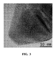
- 238000002173 high-resolution transmission electron microscopy Methods 0.000 description 6
- 229910052750 molybdenum Inorganic materials 0.000 description 6
- 239000011733 molybdenum Substances 0.000 description 6
- 239000011734 sodium Substances 0.000 description 6
- 239000000126 substance Substances 0.000 description 6
- 229910052725 zinc Inorganic materials 0.000 description 6
- 239000011787 zinc oxide Substances 0.000 description 6
- PIICEJLVQHRZGT-UHFFFAOYSA-N Ethylenediamine Chemical compound NCCN PIICEJLVQHRZGT-UHFFFAOYSA-N 0.000 description 5
- BUGBHKTXTAQXES-UHFFFAOYSA-N Selenium Chemical compound [Se] BUGBHKTXTAQXES-UHFFFAOYSA-N 0.000 description 5
- 229910005642 SnTe Inorganic materials 0.000 description 5
- XSQUKJJJFZCRTK-UHFFFAOYSA-N Urea Natural products NC(N)=O XSQUKJJJFZCRTK-UHFFFAOYSA-N 0.000 description 5
- 229910052793 cadmium Inorganic materials 0.000 description 5
- KUNSUQLRTQLHQQ-UHFFFAOYSA-N copper tin Chemical compound [Cu].[Sn] KUNSUQLRTQLHQQ-UHFFFAOYSA-N 0.000 description 5
- 239000006185 dispersion Substances 0.000 description 5
- 238000001035 drying Methods 0.000 description 5
- 229910052732 germanium Inorganic materials 0.000 description 5
- 229910052738 indium Inorganic materials 0.000 description 5
- 150000002500 ions Chemical class 0.000 description 5
- 239000000047 product Substances 0.000 description 5
- 238000000926 separation method Methods 0.000 description 5
- 229910052710 silicon Inorganic materials 0.000 description 5
- 238000000235 small-angle X-ray scattering Methods 0.000 description 5
- 239000005361 soda-lime glass Substances 0.000 description 5
- 238000005507 spraying Methods 0.000 description 5
- 238000004544 sputter deposition Methods 0.000 description 5
- 238000005406 washing Methods 0.000 description 5
- BSKHPKMHTQYZBB-UHFFFAOYSA-N 2-methylpyridine Chemical compound CC1=CC=CC=N1 BSKHPKMHTQYZBB-UHFFFAOYSA-N 0.000 description 4
- HWWYDZCSSYKIAD-UHFFFAOYSA-N 3,5-dimethylpyridine Chemical compound CC1=CN=CC(C)=C1 HWWYDZCSSYKIAD-UHFFFAOYSA-N 0.000 description 4
- ITQTTZVARXURQS-UHFFFAOYSA-N 3-methylpyridine Chemical compound CC1=CC=CN=C1 ITQTTZVARXURQS-UHFFFAOYSA-N 0.000 description 4
- LFQSCWFLJHTTHZ-UHFFFAOYSA-N Ethanol Chemical compound CCO LFQSCWFLJHTTHZ-UHFFFAOYSA-N 0.000 description 4
- MHAJPDPJQMAIIY-UHFFFAOYSA-N Hydrogen peroxide Chemical compound OO MHAJPDPJQMAIIY-UHFFFAOYSA-N 0.000 description 4
- WYURNTSHIVDZCO-UHFFFAOYSA-N Tetrahydrofuran Chemical compound C1CCOC1 WYURNTSHIVDZCO-UHFFFAOYSA-N 0.000 description 4
- 238000002056 X-ray absorption spectroscopy Methods 0.000 description 4
- ITBPIKUGMIZTJR-UHFFFAOYSA-N [bis(hydroxymethyl)amino]methanol Chemical compound OCN(CO)CO ITBPIKUGMIZTJR-UHFFFAOYSA-N 0.000 description 4
- 150000007513 acids Chemical class 0.000 description 4
- 229910052782 aluminium Inorganic materials 0.000 description 4
- 230000008901 benefit Effects 0.000 description 4
- 230000002902 bimodal effect Effects 0.000 description 4
- 229910052799 carbon Inorganic materials 0.000 description 4
- 230000008021 deposition Effects 0.000 description 4
- ZBCBWPMODOFKDW-UHFFFAOYSA-N diethanolamine Chemical compound OCCNCCO ZBCBWPMODOFKDW-UHFFFAOYSA-N 0.000 description 4
- 239000004312 hexamethylene tetramine Substances 0.000 description 4
- 235000010299 hexamethylene tetramine Nutrition 0.000 description 4
- 230000003287 optical effect Effects 0.000 description 4
- 229920000036 polyvinylpyrrolidone Polymers 0.000 description 4
- 235000013855 polyvinylpyrrolidone Nutrition 0.000 description 4
- UMJSCPRVCHMLSP-UHFFFAOYSA-N pyridine Natural products COC1=CC=CN=C1 UMJSCPRVCHMLSP-UHFFFAOYSA-N 0.000 description 4
- 239000010453 quartz Substances 0.000 description 4
- VYPSYNLAJGMNEJ-UHFFFAOYSA-N silicon dioxide Inorganic materials O=[Si]=O VYPSYNLAJGMNEJ-UHFFFAOYSA-N 0.000 description 4
- 238000010561 standard procedure Methods 0.000 description 4
- 229910052714 tellurium Inorganic materials 0.000 description 4
- DAFHKNAQFPVRKR-UHFFFAOYSA-N (3-hydroxy-2,2,4-trimethylpentyl) 2-methylpropanoate Chemical compound CC(C)C(O)C(C)(C)COC(=O)C(C)C DAFHKNAQFPVRKR-UHFFFAOYSA-N 0.000 description 3
- WUOACPNHFRMFPN-SECBINFHSA-N (S)-(-)-alpha-terpineol Chemical compound CC1=CC[C@@H](C(C)(C)O)CC1 WUOACPNHFRMFPN-SECBINFHSA-N 0.000 description 3
- QGLWBTPVKHMVHM-KTKRTIGZSA-N (z)-octadec-9-en-1-amine Chemical compound CCCCCCCC\C=C/CCCCCCCCN QGLWBTPVKHMVHM-KTKRTIGZSA-N 0.000 description 3
- RFFLAFLAYFXFSW-UHFFFAOYSA-N 1,2-dichlorobenzene Chemical compound ClC1=CC=CC=C1Cl RFFLAFLAYFXFSW-UHFFFAOYSA-N 0.000 description 3
- PAWQVTBBRAZDMG-UHFFFAOYSA-N 2-(3-bromo-2-fluorophenyl)acetic acid Chemical compound OC(=O)CC1=CC=CC(Br)=C1F PAWQVTBBRAZDMG-UHFFFAOYSA-N 0.000 description 3
- QTBSBXVTEAMEQO-UHFFFAOYSA-N Acetic acid Chemical compound CC(O)=O QTBSBXVTEAMEQO-UHFFFAOYSA-N 0.000 description 3
- YMWUJEATGCHHMB-UHFFFAOYSA-N Dichloromethane Chemical compound ClCCl YMWUJEATGCHHMB-UHFFFAOYSA-N 0.000 description 3
- RTZKZFJDLAIYFH-UHFFFAOYSA-N Diethyl ether Chemical compound CCOCC RTZKZFJDLAIYFH-UHFFFAOYSA-N 0.000 description 3
- KCXVZYZYPLLWCC-UHFFFAOYSA-N EDTA Chemical compound OC(=O)CN(CC(O)=O)CCN(CC(O)=O)CC(O)=O KCXVZYZYPLLWCC-UHFFFAOYSA-N 0.000 description 3
- XEKOWRVHYACXOJ-UHFFFAOYSA-N Ethyl acetate Chemical compound CCOC(C)=O XEKOWRVHYACXOJ-UHFFFAOYSA-N 0.000 description 3
- XEEYBQQBJWHFJM-UHFFFAOYSA-N Iron Chemical compound [Fe] XEEYBQQBJWHFJM-UHFFFAOYSA-N 0.000 description 3
- KWYHDKDOAIKMQN-UHFFFAOYSA-N N,N,N',N'-tetramethylethylenediamine Chemical compound CN(C)CCN(C)C KWYHDKDOAIKMQN-UHFFFAOYSA-N 0.000 description 3
- ZMXDDKWLCZADIW-UHFFFAOYSA-N N,N-Dimethylformamide Chemical compound CN(C)C=O ZMXDDKWLCZADIW-UHFFFAOYSA-N 0.000 description 3
- 238000003917 TEM image Methods 0.000 description 3
- 239000006096 absorbing agent Substances 0.000 description 3
- OVKDFILSBMEKLT-UHFFFAOYSA-N alpha-Terpineol Natural products CC(=C)C1(O)CCC(C)=CC1 OVKDFILSBMEKLT-UHFFFAOYSA-N 0.000 description 3
- 238000000231 atomic layer deposition Methods 0.000 description 3
- 238000005119 centrifugation Methods 0.000 description 3
- 239000000919 ceramic Substances 0.000 description 3
- 238000012512 characterization method Methods 0.000 description 3
- 238000000224 chemical solution deposition Methods 0.000 description 3
- OMZSGWSJDCOLKM-UHFFFAOYSA-N copper(II) sulfide Chemical compound [S-2].[Cu+2] OMZSGWSJDCOLKM-UHFFFAOYSA-N 0.000 description 3
- 239000008367 deionised water Substances 0.000 description 3
- 229910021641 deionized water Inorganic materials 0.000 description 3
- WNAHIZMDSQCWRP-UHFFFAOYSA-N dodecane-1-thiol Chemical compound CCCCCCCCCCCCS WNAHIZMDSQCWRP-UHFFFAOYSA-N 0.000 description 3
- DNJIEGIFACGWOD-UHFFFAOYSA-N ethyl mercaptane Natural products CCS DNJIEGIFACGWOD-UHFFFAOYSA-N 0.000 description 3
- 239000007789 gas Substances 0.000 description 3
- VLKZOEOYAKHREP-UHFFFAOYSA-N n-Hexane Chemical compound CCCCCC VLKZOEOYAKHREP-UHFFFAOYSA-N 0.000 description 3
- 239000012299 nitrogen atmosphere Substances 0.000 description 3
- 229920000642 polymer Polymers 0.000 description 3
- 238000000634 powder X-ray diffraction Methods 0.000 description 3
- 239000010944 silver (metal) Substances 0.000 description 3
- 239000001509 sodium citrate Substances 0.000 description 3
- 150000003388 sodium compounds Chemical class 0.000 description 3
- 239000002904 solvent Substances 0.000 description 3
- 238000001228 spectrum Methods 0.000 description 3
- 239000000725 suspension Substances 0.000 description 3
- NWONKYPBYAMBJT-UHFFFAOYSA-L zinc sulfate Chemical compound [Zn+2].[O-]S([O-])(=O)=O NWONKYPBYAMBJT-UHFFFAOYSA-L 0.000 description 3
- 229910000368 zinc sulfate Inorganic materials 0.000 description 3
- 229960001763 zinc sulfate Drugs 0.000 description 3
- WRIDQFICGBMAFQ-UHFFFAOYSA-N (E)-8-Octadecenoic acid Natural products CCCCCCCCCC=CCCCCCCC(O)=O WRIDQFICGBMAFQ-UHFFFAOYSA-N 0.000 description 2
- RUJPNZNXGCHGID-UHFFFAOYSA-N (Z)-beta-Terpineol Natural products CC(=C)C1CCC(C)(O)CC1 RUJPNZNXGCHGID-UHFFFAOYSA-N 0.000 description 2
- XNWFRZJHXBZDAG-UHFFFAOYSA-N 2-METHOXYETHANOL Chemical compound COCCO XNWFRZJHXBZDAG-UHFFFAOYSA-N 0.000 description 2
- POAOYUHQDCAZBD-UHFFFAOYSA-N 2-butoxyethanol Chemical compound CCCCOCCO POAOYUHQDCAZBD-UHFFFAOYSA-N 0.000 description 2
- ZNQVEEAIQZEUHB-UHFFFAOYSA-N 2-ethoxyethanol Chemical compound CCOCCO ZNQVEEAIQZEUHB-UHFFFAOYSA-N 0.000 description 2
- 229940093475 2-ethoxyethanol Drugs 0.000 description 2
- LQJBNNIYVWPHFW-UHFFFAOYSA-N 20:1omega9c fatty acid Natural products CCCCCCCCCCC=CCCCCCCCC(O)=O LQJBNNIYVWPHFW-UHFFFAOYSA-N 0.000 description 2
- WHBMMWSBFZVSSR-UHFFFAOYSA-N 3-hydroxybutyric acid Chemical compound CC(O)CC(O)=O WHBMMWSBFZVSSR-UHFFFAOYSA-N 0.000 description 2
- FAXDZWQIWUSWJH-UHFFFAOYSA-N 3-methoxypropan-1-amine Chemical compound COCCCN FAXDZWQIWUSWJH-UHFFFAOYSA-N 0.000 description 2
- OOWFYDWAMOKVSF-UHFFFAOYSA-N 3-methoxypropanenitrile Chemical compound COCCC#N OOWFYDWAMOKVSF-UHFFFAOYSA-N 0.000 description 2
- FBUIIWHYTLCORM-UHFFFAOYSA-N 3-tert-butylpyridine Chemical compound CC(C)(C)C1=CC=CN=C1 FBUIIWHYTLCORM-UHFFFAOYSA-N 0.000 description 2
- OCKGFTQIICXDQW-ZEQRLZLVSA-N 5-[(1r)-1-hydroxy-2-[4-[(2r)-2-hydroxy-2-(4-methyl-1-oxo-3h-2-benzofuran-5-yl)ethyl]piperazin-1-yl]ethyl]-4-methyl-3h-2-benzofuran-1-one Chemical compound C1=C2C(=O)OCC2=C(C)C([C@@H](O)CN2CCN(CC2)C[C@H](O)C2=CC=C3C(=O)OCC3=C2C)=C1 OCKGFTQIICXDQW-ZEQRLZLVSA-N 0.000 description 2
- QSBYPNXLFMSGKH-UHFFFAOYSA-N 9-Heptadecensaeure Natural products CCCCCCCC=CCCCCCCCC(O)=O QSBYPNXLFMSGKH-UHFFFAOYSA-N 0.000 description 2
- XKRFYHLGVUSROY-UHFFFAOYSA-N Argon Chemical compound [Ar] XKRFYHLGVUSROY-UHFFFAOYSA-N 0.000 description 2
- OKTJSMMVPCPJKN-UHFFFAOYSA-N Carbon Chemical compound [C] OKTJSMMVPCPJKN-UHFFFAOYSA-N 0.000 description 2
- HEDRZPFGACZZDS-UHFFFAOYSA-N Chloroform Chemical compound ClC(Cl)Cl HEDRZPFGACZZDS-UHFFFAOYSA-N 0.000 description 2
- 101150023635 Ctse gene Proteins 0.000 description 2
- QUSNBJAOOMFDIB-UHFFFAOYSA-N Ethylamine Chemical compound CCN QUSNBJAOOMFDIB-UHFFFAOYSA-N 0.000 description 2
- VEXZGXHMUGYJMC-UHFFFAOYSA-N Hydrochloric acid Chemical compound Cl VEXZGXHMUGYJMC-UHFFFAOYSA-N 0.000 description 2
- KFZMGEQAYNKOFK-UHFFFAOYSA-N Isopropanol Chemical compound CC(C)O KFZMGEQAYNKOFK-UHFFFAOYSA-N 0.000 description 2
- BAVYZALUXZFZLV-UHFFFAOYSA-N Methylamine Chemical compound NC BAVYZALUXZFZLV-UHFFFAOYSA-N 0.000 description 2
- LRHPLDYGYMQRHN-UHFFFAOYSA-N N-Butanol Chemical compound CCCCO LRHPLDYGYMQRHN-UHFFFAOYSA-N 0.000 description 2
- IMNFDUFMRHMDMM-UHFFFAOYSA-N N-Heptane Chemical compound CCCCCCC IMNFDUFMRHMDMM-UHFFFAOYSA-N 0.000 description 2
- UEEJHVSXFDXPFK-UHFFFAOYSA-N N-dimethylaminoethanol Chemical compound CN(C)CCO UEEJHVSXFDXPFK-UHFFFAOYSA-N 0.000 description 2
- 239000005642 Oleic acid Substances 0.000 description 2
- ZQPPMHVWECSIRJ-UHFFFAOYSA-N Oleic acid Natural products CCCCCCCCC=CCCCCCCCC(O)=O ZQPPMHVWECSIRJ-UHFFFAOYSA-N 0.000 description 2
- 229920001609 Poly(3,4-ethylenedioxythiophene) Polymers 0.000 description 2
- QAOWNCQODCNURD-UHFFFAOYSA-L Sulfate Chemical compound [O-]S([O-])(=O)=O QAOWNCQODCNURD-UHFFFAOYSA-L 0.000 description 2
- 238000000833 X-ray absorption fine structure spectroscopy Methods 0.000 description 2
- 238000002441 X-ray diffraction Methods 0.000 description 2
- 238000004833 X-ray photoelectron spectroscopy Methods 0.000 description 2
- 238000013019 agitation Methods 0.000 description 2
- 229940088601 alpha-terpineol Drugs 0.000 description 2
- 238000000149 argon plasma sintering Methods 0.000 description 2
- HQABUPZFAYXKJW-UHFFFAOYSA-N butan-1-amine Chemical compound CCCCN HQABUPZFAYXKJW-UHFFFAOYSA-N 0.000 description 2
- OKIIEJOIXGHUKX-UHFFFAOYSA-L cadmium iodide Chemical compound [Cd+2].[I-].[I-] OKIIEJOIXGHUKX-UHFFFAOYSA-L 0.000 description 2
- 239000012159 carrier gas Substances 0.000 description 2
- 238000005229 chemical vapour deposition Methods 0.000 description 2
- MVPPADPHJFYWMZ-UHFFFAOYSA-N chlorobenzene Chemical compound ClC1=CC=CC=C1 MVPPADPHJFYWMZ-UHFFFAOYSA-N 0.000 description 2
- 229910052804 chromium Inorganic materials 0.000 description 2
- 229920001577 copolymer Polymers 0.000 description 2
- JHIVVAPYMSGYDF-UHFFFAOYSA-N cyclohexanone Chemical compound O=C1CCCCC1 JHIVVAPYMSGYDF-UHFFFAOYSA-N 0.000 description 2
- BGTOWKSIORTVQH-UHFFFAOYSA-N cyclopentanone Chemical compound O=C1CCCC1 BGTOWKSIORTVQH-UHFFFAOYSA-N 0.000 description 2
- 229960002887 deanol Drugs 0.000 description 2
- VTXVGVNLYGSIAR-UHFFFAOYSA-N decane-1-thiol Chemical compound CCCCCCCCCCS VTXVGVNLYGSIAR-UHFFFAOYSA-N 0.000 description 2
- 238000000280 densification Methods 0.000 description 2
- 238000003618 dip coating Methods 0.000 description 2
- 238000009713 electroplating Methods 0.000 description 2
- 230000005669 field effect Effects 0.000 description 2
- NNRLDGQZIVUQTE-UHFFFAOYSA-N gamma-Terpineol Chemical compound CC(C)=C1CCC(C)(O)CC1 NNRLDGQZIVUQTE-UHFFFAOYSA-N 0.000 description 2
- 229910052737 gold Inorganic materials 0.000 description 2
- WQYVRQLZKVEZGA-UHFFFAOYSA-N hypochlorite Chemical compound Cl[O-] WQYVRQLZKVEZGA-UHFFFAOYSA-N 0.000 description 2
- 238000001095 inductively coupled plasma mass spectrometry Methods 0.000 description 2
- 229910052742 iron Inorganic materials 0.000 description 2
- QXJSBBXBKPUZAA-UHFFFAOYSA-N isooleic acid Natural products CCCCCCCC=CCCCCCCCCC(O)=O QXJSBBXBKPUZAA-UHFFFAOYSA-N 0.000 description 2
- 229910052745 lead Inorganic materials 0.000 description 2
- 238000005259 measurement Methods 0.000 description 2
- 229910021645 metal ion Inorganic materials 0.000 description 2
- 239000011859 microparticle Substances 0.000 description 2
- 238000003801 milling Methods 0.000 description 2
- MGFYIUFZLHCRTH-UHFFFAOYSA-N nitrilotriacetic acid Chemical compound OC(=O)CN(CC(O)=O)CC(O)=O MGFYIUFZLHCRTH-UHFFFAOYSA-N 0.000 description 2
- 231100000252 nontoxic Toxicity 0.000 description 2
- 230000003000 nontoxic effect Effects 0.000 description 2
- KZCOBXFFBQJQHH-UHFFFAOYSA-N octane-1-thiol Chemical compound CCCCCCCCS KZCOBXFFBQJQHH-UHFFFAOYSA-N 0.000 description 2
- ZQPPMHVWECSIRJ-KTKRTIGZSA-N oleic acid Chemical compound CCCCCCCC\C=C/CCCCCCCC(O)=O ZQPPMHVWECSIRJ-KTKRTIGZSA-N 0.000 description 2
- 239000011368 organic material Substances 0.000 description 2
- 229910052760 oxygen Inorganic materials 0.000 description 2
- XNLICIUVMPYHGG-UHFFFAOYSA-N pentan-2-one Chemical compound CCCC(C)=O XNLICIUVMPYHGG-UHFFFAOYSA-N 0.000 description 2
- 238000005240 physical vapour deposition Methods 0.000 description 2
- 229920001467 poly(styrenesulfonates) Polymers 0.000 description 2
- 229920001223 polyethylene glycol Polymers 0.000 description 2
- 229920001721 polyimide Polymers 0.000 description 2
- 239000001267 polyvinylpyrrolidone Substances 0.000 description 2
- 238000002360 preparation method Methods 0.000 description 2
- BDERNNFJNOPAEC-UHFFFAOYSA-N propan-1-ol Chemical compound CCCO BDERNNFJNOPAEC-UHFFFAOYSA-N 0.000 description 2
- 239000000376 reactant Substances 0.000 description 2
- NLJMYIDDQXHKNR-UHFFFAOYSA-K sodium citrate Chemical compound O.O.[Na+].[Na+].[Na+].[O-]C(=O)CC(O)(CC([O-])=O)C([O-])=O NLJMYIDDQXHKNR-UHFFFAOYSA-K 0.000 description 2
- 238000003746 solid phase reaction Methods 0.000 description 2
- 238000010671 solid-state reaction Methods 0.000 description 2
- 241000894007 species Species 0.000 description 2
- 229910052950 sphalerite Inorganic materials 0.000 description 2
- 238000004528 spin coating Methods 0.000 description 2
- QJVXKWHHAMZTBY-GCPOEHJPSA-N syringin Chemical compound COC1=CC(\C=C\CO)=CC(OC)=C1O[C@H]1[C@H](O)[C@@H](O)[C@H](O)[C@@H](CO)O1 QJVXKWHHAMZTBY-GCPOEHJPSA-N 0.000 description 2
- YLQBMQCUIZJEEH-UHFFFAOYSA-N tetrahydrofuran Natural products C=1C=COC=1 YLQBMQCUIZJEEH-UHFFFAOYSA-N 0.000 description 2
- HPGGPRDJHPYFRM-UHFFFAOYSA-J tin(iv) chloride Chemical compound Cl[Sn](Cl)(Cl)Cl HPGGPRDJHPYFRM-UHFFFAOYSA-J 0.000 description 2
- 238000007740 vapor deposition Methods 0.000 description 2
- 239000003981 vehicle Substances 0.000 description 2
- 238000004846 x-ray emission Methods 0.000 description 2
- 229910052984 zinc sulfide Inorganic materials 0.000 description 2
- POILWHVDKZOXJZ-ARJAWSKDSA-M (z)-4-oxopent-2-en-2-olate Chemical compound C\C([O-])=C\C(C)=O POILWHVDKZOXJZ-ARJAWSKDSA-M 0.000 description 1
- LZDKZFUFMNSQCJ-UHFFFAOYSA-N 1,2-diethoxyethane Chemical compound CCOCCOCC LZDKZFUFMNSQCJ-UHFFFAOYSA-N 0.000 description 1
- RKDVKSZUMVYZHH-UHFFFAOYSA-N 1,4-dioxane-2,5-dione Chemical compound O=C1COC(=O)CO1 RKDVKSZUMVYZHH-UHFFFAOYSA-N 0.000 description 1
- FXEIVSYQEOJLBU-UHFFFAOYSA-N 1-$l^{1}-selanylethanimine Chemical compound CC([Se])=N FXEIVSYQEOJLBU-UHFFFAOYSA-N 0.000 description 1
- GKWLILHTTGWKLQ-UHFFFAOYSA-N 2,3-dihydrothieno[3,4-b][1,4]dioxine Chemical compound O1CCOC2=CSC=C21 GKWLILHTTGWKLQ-UHFFFAOYSA-N 0.000 description 1
- JPKZEJXAVCJJIE-UHFFFAOYSA-N 2-sulfanylacetic acid;1-sulfanylethanol Chemical compound CC(O)S.OC(=O)CS JPKZEJXAVCJJIE-UHFFFAOYSA-N 0.000 description 1
- NECRQCBKTGZNMH-UHFFFAOYSA-N 3,5-dimethylhex-1-yn-3-ol Chemical compound CC(C)CC(C)(O)C#C NECRQCBKTGZNMH-UHFFFAOYSA-N 0.000 description 1
- WUPHOULIZUERAE-UHFFFAOYSA-N 3-(oxolan-2-yl)propanoic acid Chemical compound OC(=O)CCC1CCCO1 WUPHOULIZUERAE-UHFFFAOYSA-N 0.000 description 1
- QTBSBXVTEAMEQO-UHFFFAOYSA-M Acetate Chemical compound CC([O-])=O QTBSBXVTEAMEQO-UHFFFAOYSA-M 0.000 description 1
- VHUUQVKOLVNVRT-UHFFFAOYSA-N Ammonium hydroxide Chemical compound [NH4+].[OH-] VHUUQVKOLVNVRT-UHFFFAOYSA-N 0.000 description 1
- DKPFZGUDAPQIHT-UHFFFAOYSA-N Butyl acetate Natural products CCCCOC(C)=O DKPFZGUDAPQIHT-UHFFFAOYSA-N 0.000 description 1
- 229910004613 CdTe Inorganic materials 0.000 description 1
- KRKNYBCHXYNGOX-UHFFFAOYSA-K Citrate Chemical compound [O-]C(=O)CC(O)(CC([O-])=O)C([O-])=O KRKNYBCHXYNGOX-UHFFFAOYSA-K 0.000 description 1
- RYGMFSIKBFXOCR-UHFFFAOYSA-N Copper Chemical compound [Cu] RYGMFSIKBFXOCR-UHFFFAOYSA-N 0.000 description 1
- 229910021591 Copper(I) chloride Inorganic materials 0.000 description 1
- XFXPMWWXUTWYJX-UHFFFAOYSA-N Cyanide Chemical compound N#[C-] XFXPMWWXUTWYJX-UHFFFAOYSA-N 0.000 description 1
- XDTMQSROBMDMFD-UHFFFAOYSA-N Cyclohexane Chemical compound C1CCCCC1 XDTMQSROBMDMFD-UHFFFAOYSA-N 0.000 description 1
- XTHFKEDIFFGKHM-UHFFFAOYSA-N Dimethoxyethane Chemical compound COCCOC XTHFKEDIFFGKHM-UHFFFAOYSA-N 0.000 description 1
- KMTRUDSVKNLOMY-UHFFFAOYSA-N Ethylene carbonate Chemical compound O=C1OCCO1 KMTRUDSVKNLOMY-UHFFFAOYSA-N 0.000 description 1
- 239000004606 Fillers/Extenders Substances 0.000 description 1
- DGAQECJNVWCQMB-PUAWFVPOSA-M Ilexoside XXIX Chemical compound C[C@@H]1CC[C@@]2(CC[C@@]3(C(=CC[C@H]4[C@]3(CC[C@@H]5[C@@]4(CC[C@@H](C5(C)C)OS(=O)(=O)[O-])C)C)[C@@H]2[C@]1(C)O)C)C(=O)O[C@H]6[C@@H]([C@H]([C@@H]([C@H](O6)CO)O)O)O.[Na+] DGAQECJNVWCQMB-PUAWFVPOSA-M 0.000 description 1
- 229910021617 Indium monochloride Inorganic materials 0.000 description 1
- NHTMVDHEPJAVLT-UHFFFAOYSA-N Isooctane Chemical compound CC(C)CC(C)(C)C NHTMVDHEPJAVLT-UHFFFAOYSA-N 0.000 description 1
- SECXISVLQFMRJM-UHFFFAOYSA-N N-Methylpyrrolidone Chemical compound CN1CCCC1=O SECXISVLQFMRJM-UHFFFAOYSA-N 0.000 description 1
- 229910002651 NO3 Inorganic materials 0.000 description 1
- NHNBFGGVMKEFGY-UHFFFAOYSA-N Nitrate Chemical compound [O-][N+]([O-])=O NHNBFGGVMKEFGY-UHFFFAOYSA-N 0.000 description 1
- GRYLNZFGIOXLOG-UHFFFAOYSA-N Nitric acid Chemical compound O[N+]([O-])=O GRYLNZFGIOXLOG-UHFFFAOYSA-N 0.000 description 1
- CTQNGGLPUBDAKN-UHFFFAOYSA-N O-Xylene Chemical compound CC1=CC=CC=C1C CTQNGGLPUBDAKN-UHFFFAOYSA-N 0.000 description 1
- MUBZPKHOEPUJKR-UHFFFAOYSA-N Oxalic acid Chemical compound OC(=O)C(O)=O MUBZPKHOEPUJKR-UHFFFAOYSA-N 0.000 description 1
- 229910019142 PO4 Inorganic materials 0.000 description 1
- 229920002845 Poly(methacrylic acid) Polymers 0.000 description 1
- 229920000388 Polyphosphate Polymers 0.000 description 1
- 239000004793 Polystyrene Substances 0.000 description 1
- 229910006404 SnO 2 Inorganic materials 0.000 description 1
- 229910000831 Steel Inorganic materials 0.000 description 1
- 238000004998 X ray absorption near edge structure spectroscopy Methods 0.000 description 1
- PDYXSJSAMVACOH-UHFFFAOYSA-N [Cu].[Zn].[Sn] Chemical compound [Cu].[Zn].[Sn] PDYXSJSAMVACOH-UHFFFAOYSA-N 0.000 description 1
- ZYQNKFKPTUYGMQ-UHFFFAOYSA-N [In]=[Se].[Zn] Chemical compound [In]=[Se].[Zn] ZYQNKFKPTUYGMQ-UHFFFAOYSA-N 0.000 description 1
- PGTXKIZLOWULDJ-UHFFFAOYSA-N [Mg].[Zn] Chemical compound [Mg].[Zn] PGTXKIZLOWULDJ-UHFFFAOYSA-N 0.000 description 1
- 238000010521 absorption reaction Methods 0.000 description 1
- 230000002378 acidificating effect Effects 0.000 description 1
- 230000000996 additive effect Effects 0.000 description 1
- 239000002390 adhesive tape Substances 0.000 description 1
- 238000004220 aggregation Methods 0.000 description 1
- 230000002776 aggregation Effects 0.000 description 1
- 150000003973 alkyl amines Chemical class 0.000 description 1
- 125000000217 alkyl group Chemical group 0.000 description 1
- 150000001356 alkyl thiols Chemical class 0.000 description 1
- XAGFODPZIPBFFR-UHFFFAOYSA-N aluminium Chemical compound [Al] XAGFODPZIPBFFR-UHFFFAOYSA-N 0.000 description 1
- PNEYBMLMFCGWSK-UHFFFAOYSA-N aluminium oxide Inorganic materials [O-2].[O-2].[O-2].[Al+3].[Al+3] PNEYBMLMFCGWSK-UHFFFAOYSA-N 0.000 description 1
- 239000000908 ammonium hydroxide Substances 0.000 description 1
- 229910003481 amorphous carbon Inorganic materials 0.000 description 1
- 230000003667 anti-reflective effect Effects 0.000 description 1
- 239000003963 antioxidant agent Substances 0.000 description 1
- 230000003078 antioxidant effect Effects 0.000 description 1
- 229910052786 argon Inorganic materials 0.000 description 1
- 238000003491 array Methods 0.000 description 1
- 230000005540 biological transmission Effects 0.000 description 1
- 238000009835 boiling Methods 0.000 description 1
- BDOSMKKIYDKNTQ-UHFFFAOYSA-N cadmium atom Chemical compound [Cd] BDOSMKKIYDKNTQ-UHFFFAOYSA-N 0.000 description 1
- 229940075417 cadmium iodide Drugs 0.000 description 1
- 239000003990 capacitor Substances 0.000 description 1
- 230000015556 catabolic process Effects 0.000 description 1
- 230000003197 catalytic effect Effects 0.000 description 1
- 238000006555 catalytic reaction Methods 0.000 description 1
- 150000001768 cations Chemical class 0.000 description 1
- 210000003850 cellular structure Anatomy 0.000 description 1
- 238000010549 co-Evaporation Methods 0.000 description 1
- 229920001940 conductive polymer Polymers 0.000 description 1
- 238000001816 cooling Methods 0.000 description 1
- BWFPGXWASODCHM-UHFFFAOYSA-N copper monosulfide Chemical compound [Cu]=S BWFPGXWASODCHM-UHFFFAOYSA-N 0.000 description 1
- 229910000365 copper sulfate Inorganic materials 0.000 description 1
- OXBLHERUFWYNTN-UHFFFAOYSA-M copper(I) chloride Chemical compound [Cu]Cl OXBLHERUFWYNTN-UHFFFAOYSA-M 0.000 description 1
- ARUVKPQLZAKDPS-UHFFFAOYSA-L copper(II) sulfate Chemical compound [Cu+2].[O-][S+2]([O-])([O-])[O-] ARUVKPQLZAKDPS-UHFFFAOYSA-L 0.000 description 1
- 230000007797 corrosion Effects 0.000 description 1
- 238000005260 corrosion Methods 0.000 description 1
- 239000003431 cross linking reagent Substances 0.000 description 1
- 238000002447 crystallographic data Methods 0.000 description 1
- XUJNEKJLAYXESH-UHFFFAOYSA-N cysteine Natural products SCC(N)C(O)=O XUJNEKJLAYXESH-UHFFFAOYSA-N 0.000 description 1
- 235000018417 cysteine Nutrition 0.000 description 1
- 238000007405 data analysis Methods 0.000 description 1
- 238000013480 data collection Methods 0.000 description 1
- 238000010908 decantation Methods 0.000 description 1
- 238000000354 decomposition reaction Methods 0.000 description 1
- 238000006731 degradation reaction Methods 0.000 description 1
- 239000000412 dendrimer Substances 0.000 description 1
- 229920000736 dendritic polymer Polymers 0.000 description 1
- 239000002274 desiccant Substances 0.000 description 1
- 238000001514 detection method Methods 0.000 description 1
- 239000003989 dielectric material Substances 0.000 description 1
- 238000007598 dipping method Methods 0.000 description 1
- 239000002612 dispersion medium Substances 0.000 description 1
- 238000007606 doctor blade method Methods 0.000 description 1
- 238000004070 electrodeposition Methods 0.000 description 1
- 238000005566 electron beam evaporation Methods 0.000 description 1
- 238000010894 electron beam technology Methods 0.000 description 1
- 239000003995 emulsifying agent Substances 0.000 description 1
- 238000002149 energy-dispersive X-ray emission spectroscopy Methods 0.000 description 1
- 239000000945 filler Substances 0.000 description 1
- 238000001914 filtration Methods 0.000 description 1
- 239000011888 foil Substances 0.000 description 1
- 150000002390 heteroarenes Chemical class 0.000 description 1
- FUZZWVXGSFPDMH-UHFFFAOYSA-N hexanoic acid Chemical compound CCCCCC(O)=O FUZZWVXGSFPDMH-UHFFFAOYSA-N 0.000 description 1
- 125000000487 histidyl group Chemical group [H]N([H])C(C(=O)O*)C([H])([H])C1=C([H])N([H])C([H])=N1 0.000 description 1
- 229920001519 homopolymer Polymers 0.000 description 1
- OYQJFWIXVCUZEO-UHFFFAOYSA-N hydrogen peroxide;thiourea Chemical compound OO.NC(N)=S OYQJFWIXVCUZEO-UHFFFAOYSA-N 0.000 description 1
- XLYOFNOQVPJJNP-UHFFFAOYSA-M hydroxide Chemical compound [OH-] XLYOFNOQVPJJNP-UHFFFAOYSA-M 0.000 description 1
- 150000004679 hydroxides Chemical class 0.000 description 1
- 229920000587 hyperbranched polymer Polymers 0.000 description 1
- APFVFJFRJDLVQX-UHFFFAOYSA-N indium atom Chemical compound [In] APFVFJFRJDLVQX-UHFFFAOYSA-N 0.000 description 1
- APHGZSBLRQFRCA-UHFFFAOYSA-M indium(1+);chloride Chemical compound [In]Cl APHGZSBLRQFRCA-UHFFFAOYSA-M 0.000 description 1
- AKUCEXGLFUSJCD-UHFFFAOYSA-N indium(3+);selenium(2-) Chemical compound [Se-2].[Se-2].[Se-2].[In+3].[In+3] AKUCEXGLFUSJCD-UHFFFAOYSA-N 0.000 description 1
- PSCMQHVBLHHWTO-UHFFFAOYSA-K indium(iii) chloride Chemical compound Cl[In](Cl)Cl PSCMQHVBLHHWTO-UHFFFAOYSA-K 0.000 description 1
- AMGQUBHHOARCQH-UHFFFAOYSA-N indium;oxotin Chemical compound [In].[Sn]=O AMGQUBHHOARCQH-UHFFFAOYSA-N 0.000 description 1
- 239000011261 inert gas Substances 0.000 description 1
- 239000003112 inhibitor Substances 0.000 description 1
- 238000007641 inkjet printing Methods 0.000 description 1
- 229910010272 inorganic material Inorganic materials 0.000 description 1
- 239000011147 inorganic material Substances 0.000 description 1
- 239000012212 insulator Substances 0.000 description 1
- 230000003993 interaction Effects 0.000 description 1
- JJTUDXZGHPGLLC-UHFFFAOYSA-N lactide Chemical compound CC1OC(=O)C(C)OC1=O JJTUDXZGHPGLLC-UHFFFAOYSA-N 0.000 description 1
- 238000003760 magnetic stirring Methods 0.000 description 1
- 239000011159 matrix material Substances 0.000 description 1
- AUHZEENZYGFFBQ-UHFFFAOYSA-N mesitylene Substances CC1=CC(C)=CC(C)=C1 AUHZEENZYGFFBQ-UHFFFAOYSA-N 0.000 description 1
- 125000001827 mesitylenyl group Chemical group [H]C1=C(C(*)=C(C([H])=C1C([H])([H])[H])C([H])([H])[H])C([H])([H])[H] 0.000 description 1
- 239000002923 metal particle Substances 0.000 description 1
- 229910052976 metal sulfide Inorganic materials 0.000 description 1
- 238000007760 metering rod coating Methods 0.000 description 1
- 125000005395 methacrylic acid group Chemical group 0.000 description 1
- 229930003658 monoterpene Natural products 0.000 description 1
- 150000002773 monoterpene derivatives Chemical class 0.000 description 1
- 235000002577 monoterpenes Nutrition 0.000 description 1
- SYSQUGFVNFXIIT-UHFFFAOYSA-N n-[4-(1,3-benzoxazol-2-yl)phenyl]-4-nitrobenzenesulfonamide Chemical class C1=CC([N+](=O)[O-])=CC=C1S(=O)(=O)NC1=CC=C(C=2OC3=CC=CC=C3N=2)C=C1 SYSQUGFVNFXIIT-UHFFFAOYSA-N 0.000 description 1
- 230000007935 neutral effect Effects 0.000 description 1
- 229910017604 nitric acid Inorganic materials 0.000 description 1
- 150000004767 nitrides Chemical class 0.000 description 1
- TVMXDCGIABBOFY-UHFFFAOYSA-N octane Chemical compound CCCCCCCC TVMXDCGIABBOFY-UHFFFAOYSA-N 0.000 description 1
- 239000003960 organic solvent Substances 0.000 description 1
- 230000003647 oxidation Effects 0.000 description 1
- 238000007254 oxidation reaction Methods 0.000 description 1
- MPQXHAGKBWFSNV-UHFFFAOYSA-N oxidophosphanium Chemical class [PH3]=O MPQXHAGKBWFSNV-UHFFFAOYSA-N 0.000 description 1
- AUONHKJOIZSQGR-UHFFFAOYSA-N oxophosphane Chemical compound P=O AUONHKJOIZSQGR-UHFFFAOYSA-N 0.000 description 1
- 239000008188 pellet Substances 0.000 description 1
- VLTRZXGMWDSKGL-UHFFFAOYSA-M perchlorate Inorganic materials [O-]Cl(=O)(=O)=O VLTRZXGMWDSKGL-UHFFFAOYSA-M 0.000 description 1
- VLTRZXGMWDSKGL-UHFFFAOYSA-N perchloric acid Chemical compound OCl(=O)(=O)=O VLTRZXGMWDSKGL-UHFFFAOYSA-N 0.000 description 1
- NBIIXXVUZAFLBC-UHFFFAOYSA-K phosphate Chemical compound [O-]P([O-])([O-])=O NBIIXXVUZAFLBC-UHFFFAOYSA-K 0.000 description 1
- 239000010452 phosphate Substances 0.000 description 1
- 229910052698 phosphorus Inorganic materials 0.000 description 1
- 229920003023 plastic Polymers 0.000 description 1
- 239000004033 plastic Substances 0.000 description 1
- 239000004014 plasticizer Substances 0.000 description 1
- 229920000747 poly(lactic acid) Polymers 0.000 description 1
- 229920000768 polyamine Polymers 0.000 description 1
- 239000004417 polycarbonate Substances 0.000 description 1
- 229920000515 polycarbonate Polymers 0.000 description 1
- 229920005646 polycarboxylate Polymers 0.000 description 1
- 229920000570 polyether Polymers 0.000 description 1
- 229920006254 polymer film Polymers 0.000 description 1
- 229920000193 polymethacrylate Polymers 0.000 description 1
- 239000001205 polyphosphate Substances 0.000 description 1
- 235000011176 polyphosphates Nutrition 0.000 description 1
- 229920000379 polypropylene carbonate Polymers 0.000 description 1
- 239000002244 precipitate Substances 0.000 description 1
- 238000007639 printing Methods 0.000 description 1
- 102000004196 processed proteins & peptides Human genes 0.000 description 1
- 108090000765 processed proteins & peptides Proteins 0.000 description 1
- 238000012545 processing Methods 0.000 description 1
- 238000004549 pulsed laser deposition Methods 0.000 description 1
- 238000000746 purification Methods 0.000 description 1
- 230000005855 radiation Effects 0.000 description 1
- 238000004151 rapid thermal annealing Methods 0.000 description 1
- 239000002994 raw material Substances 0.000 description 1
- 238000007761 roller coating Methods 0.000 description 1
- 238000007650 screen-printing Methods 0.000 description 1
- SBIBMFFZSBJNJF-UHFFFAOYSA-N selenium;zinc Chemical compound [Se]=[Zn] SBIBMFFZSBJNJF-UHFFFAOYSA-N 0.000 description 1
- IYKVLICPFCEZOF-UHFFFAOYSA-N selenourea Chemical compound NC(N)=[Se] IYKVLICPFCEZOF-UHFFFAOYSA-N 0.000 description 1
- 125000004469 siloxy group Chemical group [SiH3]O* 0.000 description 1
- 239000002356 single layer Substances 0.000 description 1
- 238000007764 slot die coating Methods 0.000 description 1
- 229910052708 sodium Inorganic materials 0.000 description 1
- 229910001415 sodium ion Inorganic materials 0.000 description 1
- VPQBLCVGUWPDHV-UHFFFAOYSA-N sodium selenide Chemical compound [Na+].[Na+].[Se-2] VPQBLCVGUWPDHV-UHFFFAOYSA-N 0.000 description 1
- 229910052979 sodium sulfide Inorganic materials 0.000 description 1
- GRVFOGOEDUUMBP-UHFFFAOYSA-N sodium sulfide (anhydrous) Chemical compound [Na+].[Na+].[S-2] GRVFOGOEDUUMBP-UHFFFAOYSA-N 0.000 description 1
- 238000000527 sonication Methods 0.000 description 1
- 238000004611 spectroscopical analysis Methods 0.000 description 1
- 238000005118 spray pyrolysis Methods 0.000 description 1
- 239000003381 stabilizer Substances 0.000 description 1
- 229910001220 stainless steel Inorganic materials 0.000 description 1
- 239000010935 stainless steel Substances 0.000 description 1
- 229940071182 stannate Drugs 0.000 description 1
- 239000010959 steel Substances 0.000 description 1
- 239000011550 stock solution Substances 0.000 description 1
- 150000004763 sulfides Chemical class 0.000 description 1
- 238000005211 surface analysis Methods 0.000 description 1
- PORWMNRCUJJQNO-UHFFFAOYSA-N tellurium atom Chemical compound [Te] PORWMNRCUJJQNO-UHFFFAOYSA-N 0.000 description 1
- 238000002207 thermal evaporation Methods 0.000 description 1
- 239000002562 thickening agent Substances 0.000 description 1
- 238000002042 time-of-flight secondary ion mass spectrometry Methods 0.000 description 1
- ALRFTTOJSPMYSY-UHFFFAOYSA-N tin disulfide Chemical compound S=[Sn]=S ALRFTTOJSPMYSY-UHFFFAOYSA-N 0.000 description 1
- KHMOASUYFVRATF-UHFFFAOYSA-J tin(4+);tetrachloride;pentahydrate Chemical compound O.O.O.O.O.Cl[Sn](Cl)(Cl)Cl KHMOASUYFVRATF-UHFFFAOYSA-J 0.000 description 1
- 231100000419 toxicity Toxicity 0.000 description 1
- 230000001988 toxicity Effects 0.000 description 1
- 230000001052 transient effect Effects 0.000 description 1
- PHYFQTYBJUILEZ-IUPFWZBJSA-N triolein Chemical compound CCCCCCCC\C=C/CCCCCCCC(=O)OCC(OC(=O)CCCCCCC\C=C/CCCCCCCC)COC(=O)CCCCCCC\C=C/CCCCCCCC PHYFQTYBJUILEZ-IUPFWZBJSA-N 0.000 description 1
- HRXKRNGNAMMEHJ-UHFFFAOYSA-K trisodium citrate Chemical compound [Na+].[Na+].[Na+].[O-]C(=O)CC(O)(CC([O-])=O)C([O-])=O HRXKRNGNAMMEHJ-UHFFFAOYSA-K 0.000 description 1
- 229940038773 trisodium citrate Drugs 0.000 description 1
- GPRLSGONYQIRFK-MNYXATJNSA-N triton Chemical compound [3H+] GPRLSGONYQIRFK-MNYXATJNSA-N 0.000 description 1
- 229910052721 tungsten Inorganic materials 0.000 description 1
- 238000002491 ultra-small angle X-ray scattering Methods 0.000 description 1
- 238000009827 uniform distribution Methods 0.000 description 1
- 229910052720 vanadium Inorganic materials 0.000 description 1
- 238000009736 wetting Methods 0.000 description 1
- 239000008096 xylene Substances 0.000 description 1
- UGZADUVQMDAIAO-UHFFFAOYSA-L zinc hydroxide Chemical compound [OH-].[OH-].[Zn+2] UGZADUVQMDAIAO-UHFFFAOYSA-L 0.000 description 1
- 229910021511 zinc hydroxide Inorganic materials 0.000 description 1
- 229940007718 zinc hydroxide Drugs 0.000 description 1
- RZLVQBNCHSJZPX-UHFFFAOYSA-L zinc sulfate heptahydrate Chemical compound O.O.O.O.O.O.O.[Zn+2].[O-]S([O-])(=O)=O RZLVQBNCHSJZPX-UHFFFAOYSA-L 0.000 description 1
- UQMZPFKLYHOJDL-UHFFFAOYSA-N zinc;cadmium(2+);disulfide Chemical compound [S-2].[S-2].[Zn+2].[Cd+2] UQMZPFKLYHOJDL-UHFFFAOYSA-N 0.000 description 1
- DRDVZXDWVBGGMH-UHFFFAOYSA-N zinc;sulfide Chemical compound [S-2].[Zn+2] DRDVZXDWVBGGMH-UHFFFAOYSA-N 0.000 description 1
- 229910000859 α-Fe Inorganic materials 0.000 description 1
- DGVVWUTYPXICAM-UHFFFAOYSA-N β‐Mercaptoethanol Chemical compound OCCS DGVVWUTYPXICAM-UHFFFAOYSA-N 0.000 description 1
Images

Classifications
-
- C—CHEMISTRY; METALLURGY
- C01—INORGANIC CHEMISTRY
- C01G—COMPOUNDS CONTAINING METALS NOT COVERED BY SUBCLASSES C01D OR C01F
- C01G19/00—Compounds of tin
- C01G19/006—Compounds containing tin, with or without oxygen or hydrogen, and containing two or more other elements
-
- B—PERFORMING OPERATIONS; TRANSPORTING
- B82—NANOTECHNOLOGY
- B82B—NANOSTRUCTURES FORMED BY MANIPULATION OF INDIVIDUAL ATOMS, MOLECULES, OR LIMITED COLLECTIONS OF ATOMS OR MOLECULES AS DISCRETE UNITS; MANUFACTURE OR TREATMENT THEREOF
- B82B3/00—Manufacture or treatment of nanostructures by manipulation of individual atoms or molecules, or limited collections of atoms or molecules as discrete units
-
- B—PERFORMING OPERATIONS; TRANSPORTING
- B82—NANOTECHNOLOGY
- B82Y—SPECIFIC USES OR APPLICATIONS OF NANOSTRUCTURES; MEASUREMENT OR ANALYSIS OF NANOSTRUCTURES; MANUFACTURE OR TREATMENT OF NANOSTRUCTURES
- B82Y30/00—Nanotechnology for materials or surface science, e.g. nanocomposites
-
- C—CHEMISTRY; METALLURGY
- C01—INORGANIC CHEMISTRY
- C01B—NON-METALLIC ELEMENTS; COMPOUNDS THEREOF; METALLOIDS OR COMPOUNDS THEREOF NOT COVERED BY SUBCLASS C01C
- C01B17/00—Sulfur; Compounds thereof
-
- C—CHEMISTRY; METALLURGY
- C01—INORGANIC CHEMISTRY
- C01B—NON-METALLIC ELEMENTS; COMPOUNDS THEREOF; METALLOIDS OR COMPOUNDS THEREOF NOT COVERED BY SUBCLASS C01C
- C01B17/00—Sulfur; Compounds thereof
- C01B17/20—Methods for preparing sulfides or polysulfides, in general
-
- C—CHEMISTRY; METALLURGY
- C01—INORGANIC CHEMISTRY
- C01B—NON-METALLIC ELEMENTS; COMPOUNDS THEREOF; METALLOIDS OR COMPOUNDS THEREOF NOT COVERED BY SUBCLASS C01C
- C01B19/00—Selenium; Tellurium; Compounds thereof
- C01B19/002—Compounds containing, besides selenium or tellurium, more than one other element, with -O- and -OH not being considered as anions
-
- C—CHEMISTRY; METALLURGY
- C01—INORGANIC CHEMISTRY
- C01B—NON-METALLIC ELEMENTS; COMPOUNDS THEREOF; METALLOIDS OR COMPOUNDS THEREOF NOT COVERED BY SUBCLASS C01C
- C01B19/00—Selenium; Tellurium; Compounds thereof
- C01B19/007—Tellurides or selenides of metals
-
- C—CHEMISTRY; METALLURGY
- C01—INORGANIC CHEMISTRY
- C01G—COMPOUNDS CONTAINING METALS NOT COVERED BY SUBCLASSES C01D OR C01F
- C01G11/00—Compounds of cadmium
-
- C—CHEMISTRY; METALLURGY
- C01—INORGANIC CHEMISTRY
- C01G—COMPOUNDS CONTAINING METALS NOT COVERED BY SUBCLASSES C01D OR C01F
- C01G3/00—Compounds of copper
-
- C—CHEMISTRY; METALLURGY
- C09—DYES; PAINTS; POLISHES; NATURAL RESINS; ADHESIVES; COMPOSITIONS NOT OTHERWISE PROVIDED FOR; APPLICATIONS OF MATERIALS NOT OTHERWISE PROVIDED FOR
- C09D—COATING COMPOSITIONS, e.g. PAINTS, VARNISHES OR LACQUERS; FILLING PASTES; CHEMICAL PAINT OR INK REMOVERS; INKS; CORRECTING FLUIDS; WOODSTAINS; PASTES OR SOLIDS FOR COLOURING OR PRINTING; USE OF MATERIALS THEREFOR
- C09D11/00—Inks
- C09D11/02—Printing inks
- C09D11/03—Printing inks characterised by features other than the chemical nature of the binder
- C09D11/037—Printing inks characterised by features other than the chemical nature of the binder characterised by the pigment
-
- C—CHEMISTRY; METALLURGY
- C09—DYES; PAINTS; POLISHES; NATURAL RESINS; ADHESIVES; COMPOSITIONS NOT OTHERWISE PROVIDED FOR; APPLICATIONS OF MATERIALS NOT OTHERWISE PROVIDED FOR
- C09D—COATING COMPOSITIONS, e.g. PAINTS, VARNISHES OR LACQUERS; FILLING PASTES; CHEMICAL PAINT OR INK REMOVERS; INKS; CORRECTING FLUIDS; WOODSTAINS; PASTES OR SOLIDS FOR COLOURING OR PRINTING; USE OF MATERIALS THEREFOR
- C09D11/00—Inks
- C09D11/30—Inkjet printing inks
- C09D11/32—Inkjet printing inks characterised by colouring agents
- C09D11/322—Pigment inks
-
- H—ELECTRICITY
- H01—ELECTRIC ELEMENTS
- H01L—SEMICONDUCTOR DEVICES NOT COVERED BY CLASS H10
- H01L21/00—Processes or apparatus adapted for the manufacture or treatment of semiconductor or solid state devices or of parts thereof
- H01L21/02—Manufacture or treatment of semiconductor devices or of parts thereof
- H01L21/02104—Forming layers
- H01L21/02365—Forming inorganic semiconducting materials on a substrate
- H01L21/02518—Deposited layers
- H01L21/02521—Materials
- H01L21/02568—Chalcogenide semiconducting materials not being oxides, e.g. ternary compounds
-
- H—ELECTRICITY
- H01—ELECTRIC ELEMENTS
- H01L—SEMICONDUCTOR DEVICES NOT COVERED BY CLASS H10
- H01L21/00—Processes or apparatus adapted for the manufacture or treatment of semiconductor or solid state devices or of parts thereof
- H01L21/02—Manufacture or treatment of semiconductor devices or of parts thereof
- H01L21/02104—Forming layers
- H01L21/02365—Forming inorganic semiconducting materials on a substrate
- H01L21/02518—Deposited layers
- H01L21/02587—Structure
- H01L21/0259—Microstructure
- H01L21/02601—Nanoparticles
-
- H—ELECTRICITY
- H01—ELECTRIC ELEMENTS
- H01L—SEMICONDUCTOR DEVICES NOT COVERED BY CLASS H10
- H01L21/00—Processes or apparatus adapted for the manufacture or treatment of semiconductor or solid state devices or of parts thereof
- H01L21/02—Manufacture or treatment of semiconductor devices or of parts thereof
- H01L21/02104—Forming layers
- H01L21/02365—Forming inorganic semiconducting materials on a substrate
- H01L21/02612—Formation types
- H01L21/02617—Deposition types
- H01L21/02623—Liquid deposition
- H01L21/02628—Liquid deposition using solutions
-
- H—ELECTRICITY
- H10—SEMICONDUCTOR DEVICES; ELECTRIC SOLID-STATE DEVICES NOT OTHERWISE PROVIDED FOR
- H10F—INORGANIC SEMICONDUCTOR DEVICES SENSITIVE TO INFRARED RADIATION, LIGHT, ELECTROMAGNETIC RADIATION OF SHORTER WAVELENGTH OR CORPUSCULAR RADIATION
- H10F77/00—Constructional details of devices covered by this subclass
- H10F77/10—Semiconductor bodies
- H10F77/12—Active materials
- H10F77/126—Active materials comprising only Group I-III-VI chalcopyrite materials, e.g. CuInSe2, CuGaSe2 or CuInGaSe2 [CIGS]
-
- H—ELECTRICITY
- H10—SEMICONDUCTOR DEVICES; ELECTRIC SOLID-STATE DEVICES NOT OTHERWISE PROVIDED FOR
- H10F—INORGANIC SEMICONDUCTOR DEVICES SENSITIVE TO INFRARED RADIATION, LIGHT, ELECTROMAGNETIC RADIATION OF SHORTER WAVELENGTH OR CORPUSCULAR RADIATION
- H10F77/00—Constructional details of devices covered by this subclass
- H10F77/10—Semiconductor bodies
- H10F77/12—Active materials
- H10F77/128—Active materials comprising only Group I-II-IV-VI kesterite materials, e.g. Cu2ZnSnSe4 or Cu2ZnSnS4
-
- H—ELECTRICITY
- H10—SEMICONDUCTOR DEVICES; ELECTRIC SOLID-STATE DEVICES NOT OTHERWISE PROVIDED FOR
- H10F—INORGANIC SEMICONDUCTOR DEVICES SENSITIVE TO INFRARED RADIATION, LIGHT, ELECTROMAGNETIC RADIATION OF SHORTER WAVELENGTH OR CORPUSCULAR RADIATION
- H10F77/00—Constructional details of devices covered by this subclass
- H10F77/10—Semiconductor bodies
- H10F77/14—Shape of semiconductor bodies; Shapes, relative sizes or dispositions of semiconductor regions within semiconductor bodies
-
- C—CHEMISTRY; METALLURGY
- C01—INORGANIC CHEMISTRY
- C01P—INDEXING SCHEME RELATING TO STRUCTURAL AND PHYSICAL ASPECTS OF SOLID INORGANIC COMPOUNDS
- C01P2004/00—Particle morphology
- C01P2004/01—Particle morphology depicted by an image
- C01P2004/04—Particle morphology depicted by an image obtained by TEM, STEM, STM or AFM
-
- C—CHEMISTRY; METALLURGY
- C01—INORGANIC CHEMISTRY
- C01P—INDEXING SCHEME RELATING TO STRUCTURAL AND PHYSICAL ASPECTS OF SOLID INORGANIC COMPOUNDS
- C01P2004/00—Particle morphology
- C01P2004/60—Particles characterised by their size
- C01P2004/62—Submicrometer sized, i.e. from 0.1-1 micrometer
-
- C—CHEMISTRY; METALLURGY
- C01—INORGANIC CHEMISTRY
- C01P—INDEXING SCHEME RELATING TO STRUCTURAL AND PHYSICAL ASPECTS OF SOLID INORGANIC COMPOUNDS
- C01P2004/00—Particle morphology
- C01P2004/60—Particles characterised by their size
- C01P2004/64—Nanometer sized, i.e. from 1-100 nanometer
-
- C—CHEMISTRY; METALLURGY
- C01—INORGANIC CHEMISTRY
- C01P—INDEXING SCHEME RELATING TO STRUCTURAL AND PHYSICAL ASPECTS OF SOLID INORGANIC COMPOUNDS
- C01P2006/00—Physical properties of inorganic compounds
- C01P2006/40—Electric properties
-
- Y—GENERAL TAGGING OF NEW TECHNOLOGICAL DEVELOPMENTS; GENERAL TAGGING OF CROSS-SECTIONAL TECHNOLOGIES SPANNING OVER SEVERAL SECTIONS OF THE IPC; TECHNICAL SUBJECTS COVERED BY FORMER USPC CROSS-REFERENCE ART COLLECTIONS [XRACs] AND DIGESTS
- Y02—TECHNOLOGIES OR APPLICATIONS FOR MITIGATION OR ADAPTATION AGAINST CLIMATE CHANGE
- Y02E—REDUCTION OF GREENHOUSE GAS [GHG] EMISSIONS, RELATED TO ENERGY GENERATION, TRANSMISSION OR DISTRIBUTION
- Y02E10/00—Energy generation through renewable energy sources
- Y02E10/50—Photovoltaic [PV] energy
- Y02E10/541—CuInSe2 material PV cells
-
- Y—GENERAL TAGGING OF NEW TECHNOLOGICAL DEVELOPMENTS; GENERAL TAGGING OF CROSS-SECTIONAL TECHNOLOGIES SPANNING OVER SEVERAL SECTIONS OF THE IPC; TECHNICAL SUBJECTS COVERED BY FORMER USPC CROSS-REFERENCE ART COLLECTIONS [XRACs] AND DIGESTS
- Y10—TECHNICAL SUBJECTS COVERED BY FORMER USPC
- Y10T—TECHNICAL SUBJECTS COVERED BY FORMER US CLASSIFICATION
- Y10T428/00—Stock material or miscellaneous articles
- Y10T428/23907—Pile or nap type surface or component
- Y10T428/23986—With coating, impregnation, or bond
-
- Y—GENERAL TAGGING OF NEW TECHNOLOGICAL DEVELOPMENTS; GENERAL TAGGING OF CROSS-SECTIONAL TECHNOLOGIES SPANNING OVER SEVERAL SECTIONS OF THE IPC; TECHNICAL SUBJECTS COVERED BY FORMER USPC CROSS-REFERENCE ART COLLECTIONS [XRACs] AND DIGESTS
- Y10—TECHNICAL SUBJECTS COVERED BY FORMER USPC
- Y10T—TECHNICAL SUBJECTS COVERED BY FORMER US CLASSIFICATION
- Y10T428/00—Stock material or miscellaneous articles
- Y10T428/24—Structurally defined web or sheet [e.g., overall dimension, etc.]
- Y10T428/24479—Structurally defined web or sheet [e.g., overall dimension, etc.] including variation in thickness
- Y10T428/24612—Composite web or sheet
-
- Y—GENERAL TAGGING OF NEW TECHNOLOGICAL DEVELOPMENTS; GENERAL TAGGING OF CROSS-SECTIONAL TECHNOLOGIES SPANNING OVER SEVERAL SECTIONS OF THE IPC; TECHNICAL SUBJECTS COVERED BY FORMER USPC CROSS-REFERENCE ART COLLECTIONS [XRACs] AND DIGESTS
- Y10—TECHNICAL SUBJECTS COVERED BY FORMER USPC
- Y10T—TECHNICAL SUBJECTS COVERED BY FORMER US CLASSIFICATION
- Y10T428/00—Stock material or miscellaneous articles
- Y10T428/26—Web or sheet containing structurally defined element or component, the element or component having a specified physical dimension
- Y10T428/268—Monolayer with structurally defined element
Landscapes
- Chemical & Material Sciences (AREA)
- Engineering & Computer Science (AREA)
- Organic Chemistry (AREA)
- Inorganic Chemistry (AREA)
- General Physics & Mathematics (AREA)
- Physics & Mathematics (AREA)
- Nanotechnology (AREA)
- Condensed Matter Physics & Semiconductors (AREA)
- Manufacturing & Machinery (AREA)
- Materials Engineering (AREA)
- Computer Hardware Design (AREA)
- Microelectronics & Electronic Packaging (AREA)
- Power Engineering (AREA)
- Crystallography & Structural Chemistry (AREA)
- Wood Science & Technology (AREA)
- Life Sciences & Earth Sciences (AREA)
- General Chemical & Material Sciences (AREA)
- Chemical Kinetics & Catalysis (AREA)
- Composite Materials (AREA)
- Inks, Pencil-Leads, Or Crayons (AREA)
- Powder Metallurgy (AREA)
- Photovoltaic Devices (AREA)
- Paints Or Removers (AREA)
- Pigments, Carbon Blacks, Or Wood Stains (AREA)
Applications Claiming Priority (11)
| Application Number | Priority Date | Filing Date | Title |
|---|---|---|---|
| US26438909P | 2009-11-25 | 2009-11-25 | |
| US26438709P | 2009-11-25 | 2009-11-25 | |
| US26440409P | 2009-11-25 | 2009-11-25 | |
| US26438309P | 2009-11-25 | 2009-11-25 | |
| US26439309P | 2009-11-25 | 2009-11-25 | |
| US61/264,387 | 2009-11-25 | ||
| US61/264,389 | 2009-11-25 | ||
| US61/264,383 | 2009-11-25 | ||
| US61/264,404 | 2009-11-25 | ||
| US61/264,393 | 2009-11-25 | ||
| PCT/US2010/057566 WO2011066205A1 (en) | 2009-11-25 | 2010-11-22 | Aqueous process for producing crystalline copper chalcogenide nanoparticles, the nanoparticles so-produced, and inks and coated substrates incorporating the nanoparticles |
Publications (2)
| Publication Number | Publication Date |
|---|---|
| JP2013512311A true JP2013512311A (ja) | 2013-04-11 |
| JP2013512311A5 JP2013512311A5 (enExample) | 2013-10-03 |
Family
ID=43383645
Family Applications (1)
| Application Number | Title | Priority Date | Filing Date |
|---|---|---|---|
| JP2012541134A Withdrawn JP2013512311A (ja) | 2009-11-25 | 2010-11-22 | 結晶性銅カルコゲニドナノ粒子の水性製造方法、そのように製造されたナノ粒子、ならびにこれらのナノ粒子を組み込んだインクおよびコーテッド基板 |
Country Status (6)
| Country | Link |
|---|---|
| US (1) | US8470636B2 (enExample) |
| EP (1) | EP2504276A1 (enExample) |
| JP (1) | JP2013512311A (enExample) |
| KR (1) | KR20120098799A (enExample) |
| CN (1) | CN102612486A (enExample) |
| WO (1) | WO2011066205A1 (enExample) |
Cited By (8)
| Publication number | Priority date | Publication date | Assignee | Title |
|---|---|---|---|---|
| US8999746B2 (en) | 2013-08-08 | 2015-04-07 | Tokyo Ohka Kogyo Co., Ltd. | Method of forming metal chalcogenide dispersion, metal chalcogenide dispersion, method of producing light absorbing layer of solar cell, method of producing solar cell |
| JP2015532611A (ja) * | 2012-07-26 | 2015-11-12 | イエムエルアー ウーロプ エスアーエスImra Europe Sas | 粗大粒結晶化金属カルコゲニド膜、非晶質粒子のコロイド溶液および調製方法 |
| KR20160081102A (ko) * | 2014-12-30 | 2016-07-08 | 삼성전자주식회사 | 2차원 물질층을 포함하는 전자소자 및 잉크젯 프린팅을 이용한 전자소자의 제조방법 |
| KR20160149577A (ko) * | 2015-06-18 | 2016-12-28 | 연세대학교 산학협력단 | 전이금속 칼코겐화물 구조체 및 그 제조방법 |
| WO2017203938A1 (ja) * | 2016-05-25 | 2017-11-30 | 株式会社日本触媒 | 熱電変換材料、熱電変換素子、熱電変換材料用粉体、及び熱電変換材料の製造方法 |
| US9856382B2 (en) | 2014-10-30 | 2018-01-02 | Tokyo Ohka Kogyo Co. Ltd. | Homogeneous coating solution and production method thereof, light-absorbing layer of solar cell and production method thereof, and solar cell and production method thereof |
| JP2018140934A (ja) * | 2014-01-30 | 2018-09-13 | ナノコ テクノロジーズ リミテッド | ナトリウム又はアンチモンがドープされたナノ粒子 |
| JP2018142685A (ja) * | 2016-05-25 | 2018-09-13 | 株式会社日本触媒 | 熱電変換材料、熱電変換素子、熱電変換材料用粉体、及び熱電変換材料の製造方法 |
Families Citing this family (62)
| Publication number | Priority date | Publication date | Assignee | Title |
|---|---|---|---|---|
| US8524524B2 (en) * | 2010-04-22 | 2013-09-03 | General Electric Company | Methods for forming back contact electrodes for cadmium telluride photovoltaic cells |
| FR2964044B1 (fr) * | 2010-08-26 | 2012-09-14 | Commissariat Energie Atomique | Emulsion de metal liquide |
| WO2012075259A1 (en) * | 2010-12-03 | 2012-06-07 | E. I. Du Pont De Nemours And Company | Molecular precursors and processes for preparing copper indium gallium sulfide/selenide coatings and films |
| CN102675960B (zh) * | 2011-03-08 | 2015-08-05 | 深圳市尊业纳米材料有限公司 | 一种纳米铜锡合金导电油墨及其制备方法和使用方法 |
| FR2972443B1 (fr) * | 2011-03-09 | 2016-10-21 | Univ Paul Sabatier - Toulouse Iii (Ups) | Dispersion colloidale d'un materiau a l'etat divise forme de chalcogenure metallique dans un milieu aqueux, materiau a l'etat divise et leurs utilisations |
| US8771555B2 (en) | 2011-05-06 | 2014-07-08 | Neo Solar Power Corp. | Ink composition |
| FR2975223B1 (fr) * | 2011-05-10 | 2016-12-23 | Electricite De France | Traitement thermique par injection d'un gaz caloporteur. |
| JP2012250889A (ja) * | 2011-06-06 | 2012-12-20 | Toyota Motor Corp | 半導体粒子及びその製造方法 |
| JP5687343B2 (ja) * | 2011-06-27 | 2015-03-18 | 京セラ株式会社 | 半導体層の製造方法、光電変換装置の製造方法および半導体原料 |
| US20130037110A1 (en) * | 2011-08-10 | 2013-02-14 | International Business Machines Corporation | Particle-Based Precursor Formation Method and Photovoltaic Device Thereof |
| US9368660B2 (en) * | 2011-08-10 | 2016-06-14 | International Business Machines Corporation | Capping layers for improved crystallization |
| US8551802B2 (en) * | 2011-09-12 | 2013-10-08 | Intermolecular, Inc. | Laser annealing for thin film solar cells |
| JP2013064108A (ja) * | 2011-09-16 | 2013-04-11 | Delsolar Co Ltd | インク組成物及びその形成方法 |
| ES2402313B1 (es) * | 2011-09-30 | 2014-03-04 | Universitat Jaume I De Castellón | Tintas para la obtención "in situ" de calcógenos y/o calcogenuros que dan lugar a capas de semiconductores, su obtención y modo de empleo |
| EP2762444A4 (en) * | 2011-09-30 | 2015-06-10 | Toppan Printing Co Ltd | INK FOR PRODUCING A COMPOSITE THIN-FINISHED LAYER AND PRODUCTION METHOD THEREFOR |
| EP2786419B1 (en) * | 2011-11-30 | 2020-02-12 | Konica Minolta Laboratory U.S.A., Inc. | Method of manufacturing a photovoltaic device |
| US20130217211A1 (en) * | 2012-02-21 | 2013-08-22 | Aqt Solar, Inc. | Controlled-Pressure Process for Production of CZTS Thin-Films |
| US9573809B2 (en) * | 2012-03-30 | 2017-02-21 | Micron Technology, Inc. | Method of forming a metal chalcogenide material and methods of forming memory cells including same |
| EP2647595A2 (en) * | 2012-04-03 | 2013-10-09 | Neo Solar Power Corp. | Ink composition, chalcogenide semiconductor film, photovoltaic device and methods for forming the same |
| WO2013172949A1 (en) * | 2012-05-14 | 2013-11-21 | E. I. Du Pont De Nemours And Company | Dispersible metal chalcogenide nanoparticles |
| EP2870621B1 (en) | 2012-07-09 | 2018-12-26 | Nanoco Technologies, Ltd. | Group 13 selenide nanoparticles |
| US8741688B2 (en) | 2012-07-24 | 2014-06-03 | Micron Technology, Inc. | Methods of forming a metal chalcogenide material |
| US8871560B2 (en) * | 2012-08-09 | 2014-10-28 | International Business Machines Corporation | Plasma annealing of thin film solar cells |
| US10752514B2 (en) | 2012-09-07 | 2020-08-25 | Cornell University | Metal chalcogenide synthesis method and applications |
| JP6008736B2 (ja) * | 2012-12-26 | 2016-10-19 | 富士フイルム株式会社 | 半導体膜、半導体膜の製造方法、太陽電池、発光ダイオード、薄膜トランジスタおよび電子デバイス |
| KR101960945B1 (ko) * | 2013-03-04 | 2019-03-20 | 나노코 테크놀로지스 리미티드 | 박막 태양 전지를 위한 구리-인듐-갈륨-칼코게나이드 나노 입자 전구체 |
| CN108383090A (zh) * | 2013-03-15 | 2018-08-10 | 纳米技术有限公司 | Cu2XSnY4纳米粒子 |
| KR101716367B1 (ko) * | 2013-03-15 | 2017-03-14 | 나노코 테크놀로지스 리미티드 | Cu2ZnSnS4 나노 입자들 |
| US9634161B2 (en) | 2013-05-01 | 2017-04-25 | Delaware State University | Nanoscale precursors for synthesis of Fe2(Si,Ge)(S,Se)4 crystalline particles and layers |
| US9552985B2 (en) * | 2013-08-09 | 2017-01-24 | Japan Advanced Institute Of Science And Technology | Oxide semiconductor layer and production method therefor, oxide semiconductor precursor, oxide semiconductor layer, semiconductor element, and electronic device |
| WO2015030275A1 (ko) * | 2013-08-30 | 2015-03-05 | 한국에너지기술연구원 | 이성분계 나노입자를 포함하는 슬러리의 숙성 단계가 도입된 ci(g)s계 박막의 제조방법 및 그 방법에 의해 제조된 ci(g)s계 박막 |
| KR101650049B1 (ko) | 2013-09-12 | 2016-08-22 | 주식회사 엘지화학 | 태양전지 광흡수층 제조용 금속 칼코게나이드 나노 입자 및 이의 제조방법 |
| CN103803632B (zh) * | 2014-02-28 | 2016-04-06 | 上海海事大学 | 一种碳包覆光热转换纳米材料的制备方法 |
| US10888836B2 (en) * | 2014-07-25 | 2021-01-12 | Chemical and Metal Technologies LLC | Extraction of target materials using CZTS sorbent |
| WO2016053016A1 (ko) * | 2014-09-29 | 2016-04-07 | 이화여자대학교 산학협력단 | CZTSe계 박막 및 이의 제조 방법, 및 상기 CZTSe계 박막을 이용한 태양전지 |
| US10767112B2 (en) * | 2015-01-15 | 2020-09-08 | The Trustees Of The Columbia University In The City Of New York | Methods of producing metal sulfides, metal selenides, and metal sulfides/selenides having controlled architectures using kinetic control |
| FR3039531A1 (enExample) * | 2015-07-28 | 2017-02-03 | Nexdot | |
| KR102613046B1 (ko) * | 2015-10-06 | 2023-12-12 | 삼성전자주식회사 | 금속 칼코게나이드 나노입자 및 그 제조방법 |
| US10578572B2 (en) | 2016-01-19 | 2020-03-03 | Invensense, Inc. | CMOS integrated microheater for a gas sensor device |
| CN106025056A (zh) * | 2016-06-12 | 2016-10-12 | 电子科技大学 | 一种锡硫化合物热电材料的制备方法 |
| US10217888B2 (en) * | 2016-10-06 | 2019-02-26 | International Business Machines Corporation | Solution-phase inclusion of silver into chalcogenide semiconductor inks |
| EP3523248A1 (en) * | 2016-10-07 | 2019-08-14 | Haldor Topsøe A/S | KESTERITE MATERIAL OF CZTS, CZTSe OR CZTSSe TYPE |
| CN106505114A (zh) * | 2016-11-03 | 2017-03-15 | 中国科学院兰州化学物理研究所 | 一种铜锡硫光吸收层薄膜材料的制备方法 |
| US10383967B2 (en) | 2016-11-30 | 2019-08-20 | Invensense, Inc. | Substance sensing with tracers |
| KR101874227B1 (ko) * | 2017-01-18 | 2018-08-02 | 한양대학교 에리카산학협력단 | 구리 칼코지나이드 광 흡수체 및 광 흡수 필름, 및 그들의 제조 방법. |
| KR102038552B1 (ko) * | 2017-11-16 | 2019-10-30 | 한국세라믹기술원 | 전이금속 칼코겐화합물을 이용한 전계 효과형 트랜지스터의 제조 방법 |
| CN108383150B (zh) * | 2018-03-01 | 2020-10-30 | 复旦大学 | 一种硫化锌纳米材料的制备方法 |
| CN108249475B (zh) * | 2018-03-01 | 2020-10-30 | 复旦大学 | 一种铜铟硫纳米材料的简易制备方法 |
| WO2019228620A1 (en) * | 2018-05-30 | 2019-12-05 | Toyota Motor Europe | Inks comprising nanoparticles for high-performance inkjet-printed optoelectronics |
| RU2695208C1 (ru) * | 2018-07-17 | 2019-07-22 | Федеральное государственное бюджетное учреждение науки Институт проблем химической физики Российской академии наук (ИПХФ РАН) | Способ получения монозеренных кестеритных порошков |
| RU2718124C1 (ru) * | 2019-06-10 | 2020-03-30 | Федеральное государственное бюджетное учреждение науки Институт проблем химической физики Российской Академии наук (ФГБУН ИПХФ РАН) | Способ получения монозеренных кестеритных порошков из тройных халькогенидов меди и олова и соединений цинка |
| CN113013314B (zh) * | 2019-12-20 | 2022-12-13 | 中国科学院上海硅酸盐研究所 | 一种p型高性能Cu-Sn-S类金刚石结构热电材料及其制备方法 |
| CN115348948B (zh) * | 2020-03-11 | 2024-11-08 | 约翰内斯堡威特沃特斯兰德大学 | 碱金属四元纳米材料 |
| US11492547B2 (en) | 2020-06-04 | 2022-11-08 | UbiQD, Inc. | Low-PH nanoparticles and ligands |
| CN111755323B (zh) * | 2020-07-07 | 2023-07-21 | 内蒙古大学 | 一种铜锌锡硫太阳电池吸收层薄膜的制备方法 |
| CN112142097B (zh) * | 2020-08-31 | 2021-10-29 | 武汉理工大学 | 三水合锡酸镉及其制备方法和应用 |
| CN112279293B (zh) * | 2020-11-02 | 2023-08-25 | 贵州理工学院 | 一种硫化铜纳米材料的制备方法 |
| CN113517370B (zh) * | 2021-06-11 | 2022-10-14 | 上海应用技术大学 | 一种异质构型太阳能电池结构及其制备方法与应用 |
| CN113371754B (zh) * | 2021-06-23 | 2022-06-10 | 石久光学科技发展(北京)有限公司 | 一种高纯度锡酸镉粉体及其制备方法 |
| CN114436318B (zh) * | 2022-01-07 | 2023-10-31 | 安徽师范大学 | 一种水相合成制备单分散Cu2-xS纳米晶的方法 |
| CN114759140B (zh) * | 2022-04-13 | 2025-09-09 | 西北师范大学 | 一种铜锡硫(cts)忆阻器及其制备方法 |
| CN114933327B (zh) * | 2022-06-13 | 2023-12-01 | 佛山(华南)新材料研究院 | 一种制氢材料及其制备方法、应用 |
Family Cites Families (2)
| Publication number | Priority date | Publication date | Assignee | Title |
|---|---|---|---|---|
| FR2921661B1 (fr) * | 2007-10-01 | 2013-05-31 | Centre Nat Rech Scient | Solide hybride organique inorganique a surface modifiee. |
| US20090305449A1 (en) * | 2007-12-06 | 2009-12-10 | Brent Bollman | Methods and Devices For Processing A Precursor Layer In a Group VIA Environment |
-
2010
- 2010-11-22 WO PCT/US2010/057566 patent/WO2011066205A1/en not_active Ceased
- 2010-11-22 US US13/511,699 patent/US8470636B2/en not_active Expired - Fee Related
- 2010-11-22 KR KR20127016243A patent/KR20120098799A/ko not_active Withdrawn
- 2010-11-22 EP EP10787216A patent/EP2504276A1/en not_active Withdrawn
- 2010-11-22 CN CN2010800521136A patent/CN102612486A/zh active Pending
- 2010-11-22 JP JP2012541134A patent/JP2013512311A/ja not_active Withdrawn
Cited By (13)
| Publication number | Priority date | Publication date | Assignee | Title |
|---|---|---|---|---|
| JP2015532611A (ja) * | 2012-07-26 | 2015-11-12 | イエムエルアー ウーロプ エスアーエスImra Europe Sas | 粗大粒結晶化金属カルコゲニド膜、非晶質粒子のコロイド溶液および調製方法 |
| US8999746B2 (en) | 2013-08-08 | 2015-04-07 | Tokyo Ohka Kogyo Co., Ltd. | Method of forming metal chalcogenide dispersion, metal chalcogenide dispersion, method of producing light absorbing layer of solar cell, method of producing solar cell |
| JP2018140934A (ja) * | 2014-01-30 | 2018-09-13 | ナノコ テクノロジーズ リミテッド | ナトリウム又はアンチモンがドープされたナノ粒子 |
| US9856382B2 (en) | 2014-10-30 | 2018-01-02 | Tokyo Ohka Kogyo Co. Ltd. | Homogeneous coating solution and production method thereof, light-absorbing layer of solar cell and production method thereof, and solar cell and production method thereof |
| US10460935B2 (en) | 2014-12-30 | 2019-10-29 | Samsung Electronics Co., Ltd. | Electronic device having two-dimensional (2D) material layer and method of manufacturing the electronic device by inkjet printing |
| KR20160081102A (ko) * | 2014-12-30 | 2016-07-08 | 삼성전자주식회사 | 2차원 물질층을 포함하는 전자소자 및 잉크젯 프린팅을 이용한 전자소자의 제조방법 |
| JP2016127267A (ja) * | 2014-12-30 | 2016-07-11 | 三星電子株式会社Samsung Electronics Co.,Ltd. | 二次元物質層を含む電子素子、及びインクジェットプリンティングを利用した電子素子の製造方法 |
| KR102412965B1 (ko) * | 2014-12-30 | 2022-06-24 | 삼성전자주식회사 | 2차원 물질층을 포함하는 전자소자 및 잉크젯 프린팅을 이용한 전자소자의 제조방법 |
| KR20160149577A (ko) * | 2015-06-18 | 2016-12-28 | 연세대학교 산학협력단 | 전이금속 칼코겐화물 구조체 및 그 제조방법 |
| KR101708260B1 (ko) | 2015-06-18 | 2017-02-20 | 연세대학교 산학협력단 | 전이금속 칼코겐화물 구조체 및 그 제조방법 |
| WO2017203938A1 (ja) * | 2016-05-25 | 2017-11-30 | 株式会社日本触媒 | 熱電変換材料、熱電変換素子、熱電変換材料用粉体、及び熱電変換材料の製造方法 |
| JP2018142685A (ja) * | 2016-05-25 | 2018-09-13 | 株式会社日本触媒 | 熱電変換材料、熱電変換素子、熱電変換材料用粉体、及び熱電変換材料の製造方法 |
| US11631794B2 (en) | 2016-05-25 | 2023-04-18 | Nippon Shokubai Co., Ltd. | Thermoelectric material, thermoelectric device, powder for thermoelectric material, and method for producing thermoelectric material |
Also Published As
| Publication number | Publication date |
|---|---|
| US20120288987A1 (en) | 2012-11-15 |
| WO2011066205A1 (en) | 2011-06-03 |
| KR20120098799A (ko) | 2012-09-05 |
| CN102612486A (zh) | 2012-07-25 |
| US8470636B2 (en) | 2013-06-25 |
| EP2504276A1 (en) | 2012-10-03 |
Similar Documents
| Publication | Publication Date | Title |
|---|---|---|
| US8470636B2 (en) | Aqueous process for producing crystalline copper chalcogenide nanoparticles, the nanoparticles so-produced, and inks and coated substrates incorporating the nanoparticles | |
| US9105796B2 (en) | CZTS/Se precursor inks and methods for preparing CZTS/Se thin films and CZTS/Se-based photovoltaic cells | |
| US20120220066A1 (en) | Czts/se precursor inks and methods for preparing czts/se thin films and czts/se-based photovoltaic cells | |
| TWI460281B (zh) | 奈米粒子材料之製備 | |
| JP2013544038A (ja) | カルコゲン含有半導体を製造するためのインク及び方法 | |
| JP6312668B2 (ja) | 非晶質粒子のコロイド溶液の調製方法 | |
| US20140144500A1 (en) | Semiconductor inks films, coated substrates and methods of preparation | |
| US20130037111A1 (en) | Process for Preparation of Elemental Chalcogen Solutions and Method of Employing Said Solutions in Preparation of Kesterite Films | |
| US20140048137A1 (en) | Process for preparing coated substrates and photovoltaic devices | |
| US20140220728A1 (en) | Methods of forming semiconductor films including i2-ii-iv-vi4 and i2-(ii,iv)-iv-vi4 semiconductor films and electronic devices including the semiconductor films | |
| JP6688832B2 (ja) | アンチモンがドープされたナノ粒子 | |
| JP2012527401A (ja) | 銅亜鉛スズカルコゲナイドナノ粒子 | |
| US20150118144A1 (en) | Dispersible metal chalcogenide nanoparticles | |
| WO2012075276A1 (en) | Copper indium gallium sulfide/selenide inks, layers, and films and processes for preparing coated substrates and photovoltaic devices | |
| JP5317648B2 (ja) | 薄膜太陽電池の製法 | |
| JP5213777B2 (ja) | 薄膜太陽電池の製法 | |
| TW201502075A (zh) | 奈米顆粒、墨水及製造與使用方法 |
Legal Events
| Date | Code | Title | Description |
|---|---|---|---|
| A521 | Request for written amendment filed |
Free format text: JAPANESE INTERMEDIATE CODE: A523 Effective date: 20130813 |
|
| A621 | Written request for application examination |
Free format text: JAPANESE INTERMEDIATE CODE: A621 Effective date: 20130813 |
|
| A977 | Report on retrieval |
Free format text: JAPANESE INTERMEDIATE CODE: A971007 Effective date: 20140530 |
|
| A761 | Written withdrawal of application |
Free format text: JAPANESE INTERMEDIATE CODE: A761 Effective date: 20140625 |