KR20120098799A - 결정형 구리 칼코게나이드 나노입자의 수성 제조 방법, 그렇게 제조된 나노입자, 및 나노입자를 포함하는 잉크 및 코팅된 기재 - Google Patents
결정형 구리 칼코게나이드 나노입자의 수성 제조 방법, 그렇게 제조된 나노입자, 및 나노입자를 포함하는 잉크 및 코팅된 기재 Download PDFInfo
- Publication number
- KR20120098799A KR20120098799A KR20127016243A KR20127016243A KR20120098799A KR 20120098799 A KR20120098799 A KR 20120098799A KR 20127016243 A KR20127016243 A KR 20127016243A KR 20127016243 A KR20127016243 A KR 20127016243A KR 20120098799 A KR20120098799 A KR 20120098799A
- Authority
- KR
- South Korea
- Prior art keywords
- metal chalcogenide
- nanoparticles
- metal
- crystalline
- selenide
- Prior art date
- Legal status (The legal status is an assumption and is not a legal conclusion. Google has not performed a legal analysis and makes no representation as to the accuracy of the status listed.)
- Withdrawn
Links
- 239000002105 nanoparticle Substances 0.000 title claims abstract description 128
- 238000000034 method Methods 0.000 title claims abstract description 56
- 239000000758 substrate Substances 0.000 title claims description 47
- -1 copper chalcogenide Chemical class 0.000 title claims description 7
- 230000008569 process Effects 0.000 title abstract description 6
- 239000010949 copper Substances 0.000 title description 40
- 239000000976 ink Substances 0.000 title description 36
- 229910052802 copper Inorganic materials 0.000 title description 12
- 229910052751 metal Inorganic materials 0.000 claims abstract description 229
- 239000002184 metal Substances 0.000 claims abstract description 229
- 150000004770 chalcogenides Chemical class 0.000 claims abstract description 193
- 239000002245 particle Substances 0.000 claims abstract description 106
- WILFBXOGIULNAF-UHFFFAOYSA-N copper sulfanylidenetin zinc Chemical compound [Sn]=S.[Zn].[Cu] WILFBXOGIULNAF-UHFFFAOYSA-N 0.000 claims abstract description 13
- SEAVSGQBBULBCJ-UHFFFAOYSA-N [Sn]=S.[Cu] Chemical compound [Sn]=S.[Cu] SEAVSGQBBULBCJ-UHFFFAOYSA-N 0.000 claims abstract description 10
- 239000010410 layer Substances 0.000 claims description 73
- 239000000203 mixture Chemical class 0.000 claims description 54
- 238000010438 heat treatment Methods 0.000 claims description 39
- 239000000463 material Substances 0.000 claims description 34
- 239000011541 reaction mixture Substances 0.000 claims description 28
- 238000000576 coating method Methods 0.000 claims description 27
- 239000003446 ligand Substances 0.000 claims description 25
- 150000003346 selenoethers Chemical class 0.000 claims description 25
- 150000003839 salts Chemical class 0.000 claims description 23
- 239000011248 coating agent Substances 0.000 claims description 22
- XLYOFNOQVPJJNP-UHFFFAOYSA-N water Substances O XLYOFNOQVPJJNP-UHFFFAOYSA-N 0.000 claims description 22
- 239000007864 aqueous solution Substances 0.000 claims description 21
- 229910052798 chalcogen Inorganic materials 0.000 claims description 21
- 150000001787 chalcogens Chemical class 0.000 claims description 21
- 239000012530 fluid Substances 0.000 claims description 19
- 238000000151 deposition Methods 0.000 claims description 12
- 150000001875 compounds Chemical class 0.000 claims description 11
- 238000003756 stirring Methods 0.000 claims description 11
- QGZKDVFQNNGYKY-UHFFFAOYSA-N Ammonia Chemical compound N QGZKDVFQNNGYKY-UHFFFAOYSA-N 0.000 claims description 10
- 239000002585 base Substances 0.000 claims description 8
- 239000004094 surface-active agent Substances 0.000 claims description 8
- 150000001412 amines Chemical class 0.000 claims description 7
- 229910052733 gallium Inorganic materials 0.000 claims description 7
- 150000003573 thiols Chemical class 0.000 claims description 6
- UCKMPCXJQFINFW-UHFFFAOYSA-N Sulphide Chemical compound [S-2] UCKMPCXJQFINFW-UHFFFAOYSA-N 0.000 claims description 5
- 229910021529 ammonia Inorganic materials 0.000 claims description 5
- 239000002270 dispersing agent Substances 0.000 claims description 5
- 150000007524 organic acids Chemical class 0.000 claims description 5
- 235000005985 organic acids Nutrition 0.000 claims description 5
- GYSDUVRPSWKYDJ-UHFFFAOYSA-N selinone Chemical compound C1=CC(OCC=C(C)C)=CC=C1C1OC2=CC(O)=CC(O)=C2C(=O)C1 GYSDUVRPSWKYDJ-UHFFFAOYSA-N 0.000 claims description 5
- RWSOTUBLDIXVET-UHFFFAOYSA-N Dihydrogen sulfide Chemical compound S RWSOTUBLDIXVET-UHFFFAOYSA-N 0.000 claims description 4
- 239000000654 additive Substances 0.000 claims description 4
- 239000011230 binding agent Substances 0.000 claims description 4
- LCUOIYYHNRBAFS-UHFFFAOYSA-N copper;sulfanylideneindium Chemical compound [Cu].[In]=S LCUOIYYHNRBAFS-UHFFFAOYSA-N 0.000 claims description 4
- 239000002019 doping agent Substances 0.000 claims description 4
- 239000012799 electrically-conductive coating Substances 0.000 claims description 4
- 150000003958 selenols Chemical class 0.000 claims description 4
- GYHNNYVSQQEPJS-UHFFFAOYSA-N Gallium Chemical compound [Ga] GYHNNYVSQQEPJS-UHFFFAOYSA-N 0.000 claims description 3
- 150000001242 acetic acid derivatives Chemical class 0.000 claims description 3
- 150000003863 ammonium salts Chemical class 0.000 claims description 3
- 150000001879 copper Chemical class 0.000 claims description 3
- HVMJUDPAXRRVQO-UHFFFAOYSA-N copper indium Chemical compound [Cu].[In] HVMJUDPAXRRVQO-UHFFFAOYSA-N 0.000 claims description 3
- 150000004820 halides Chemical class 0.000 claims description 3
- 239000007788 liquid Substances 0.000 claims description 3
- 150000002825 nitriles Chemical class 0.000 claims description 3
- ATJFFYVFTNAWJD-UHFFFAOYSA-N Tin Chemical class [Sn] ATJFFYVFTNAWJD-UHFFFAOYSA-N 0.000 claims description 2
- 150000001298 alcohols Chemical class 0.000 claims description 2
- 150000001335 aliphatic alkanes Chemical class 0.000 claims description 2
- 229910052783 alkali metal Inorganic materials 0.000 claims description 2
- 150000001408 amides Chemical class 0.000 claims description 2
- 150000001735 carboxylic acids Chemical class 0.000 claims description 2
- 150000002148 esters Chemical class 0.000 claims description 2
- 150000002170 ethers Chemical class 0.000 claims description 2
- 150000002390 heteroarenes Chemical class 0.000 claims description 2
- 229910000037 hydrogen sulfide Inorganic materials 0.000 claims description 2
- 150000002576 ketones Chemical class 0.000 claims description 2
- 150000003751 zinc Chemical class 0.000 claims description 2
- 229910052977 alkali metal sulfide Inorganic materials 0.000 claims 1
- 239000006117 anti-reflective coating Substances 0.000 claims 1
- 150000002258 gallium Chemical class 0.000 claims 1
- 150000002471 indium Chemical class 0.000 claims 1
- SPVXKVOXSXTJOY-UHFFFAOYSA-N selane Chemical compound [SeH2] SPVXKVOXSXTJOY-UHFFFAOYSA-N 0.000 claims 1
- 229910000058 selane Inorganic materials 0.000 claims 1
- 239000002243 precursor Substances 0.000 abstract description 12
- 150000004771 selenides Chemical class 0.000 abstract 2
- 239000010408 film Substances 0.000 description 45
- IJGRMHOSHXDMSA-UHFFFAOYSA-N Atomic nitrogen Chemical compound N#N IJGRMHOSHXDMSA-UHFFFAOYSA-N 0.000 description 30
- 229910052717 sulfur Inorganic materials 0.000 description 30
- 239000012298 atmosphere Substances 0.000 description 24
- 230000015572 biosynthetic process Effects 0.000 description 22
- 239000011669 selenium Substances 0.000 description 22
- NINIDFKCEFEMDL-UHFFFAOYSA-N Sulfur Chemical compound [S] NINIDFKCEFEMDL-UHFFFAOYSA-N 0.000 description 21
- 239000011593 sulfur Substances 0.000 description 20
- 239000010409 thin film Substances 0.000 description 19
- 238000002474 experimental method Methods 0.000 description 18
- 238000000137 annealing Methods 0.000 description 17
- 239000003795 chemical substances by application Substances 0.000 description 17
- OKKJLVBELUTLKV-UHFFFAOYSA-N Methanol Chemical compound OC OKKJLVBELUTLKV-UHFFFAOYSA-N 0.000 description 16
- 229910052757 nitrogen Inorganic materials 0.000 description 16
- 239000000243 solution Substances 0.000 description 16
- 239000002609 medium Substances 0.000 description 14
- 239000000843 powder Substances 0.000 description 14
- 239000000126 substance Substances 0.000 description 14
- 238000003786 synthesis reaction Methods 0.000 description 14
- 239000004065 semiconductor Substances 0.000 description 13
- HEMHJVSKTPXQMS-UHFFFAOYSA-M Sodium hydroxide Chemical compound [OH-].[Na+] HEMHJVSKTPXQMS-UHFFFAOYSA-M 0.000 description 12
- XLOMVQKBTHCTTD-UHFFFAOYSA-N Zinc monoxide Chemical compound [Zn]=O XLOMVQKBTHCTTD-UHFFFAOYSA-N 0.000 description 12
- 238000004458 analytical method Methods 0.000 description 12
- 238000004140 cleaning Methods 0.000 description 12
- 238000009826 distribution Methods 0.000 description 12
- 239000000523 sample Substances 0.000 description 12
- UMGDCJDMYOKAJW-UHFFFAOYSA-N thiourea Chemical compound NC(N)=S UMGDCJDMYOKAJW-UHFFFAOYSA-N 0.000 description 12
- 239000011135 tin Substances 0.000 description 12
- 229910052711 selenium Inorganic materials 0.000 description 11
- 239000007787 solid Substances 0.000 description 11
- 239000011701 zinc Substances 0.000 description 11
- HZAXFHJVJLSVMW-UHFFFAOYSA-N 2-Aminoethan-1-ol Chemical compound NCCO HZAXFHJVJLSVMW-UHFFFAOYSA-N 0.000 description 10
- GSEJCLTVZPLZKY-UHFFFAOYSA-N Triethanolamine Chemical compound OCCN(CCO)CCO GSEJCLTVZPLZKY-UHFFFAOYSA-N 0.000 description 10
- 150000002739 metals Chemical class 0.000 description 10
- CWERGRDVMFNCDR-UHFFFAOYSA-N thioglycolic acid Chemical compound OC(=O)CS CWERGRDVMFNCDR-UHFFFAOYSA-N 0.000 description 10
- WEVYAHXRMPXWCK-UHFFFAOYSA-N Acetonitrile Chemical compound CC#N WEVYAHXRMPXWCK-UHFFFAOYSA-N 0.000 description 9
- 238000006243 chemical reaction Methods 0.000 description 9
- 239000011521 glass Substances 0.000 description 9
- YUKQRDCYNOVPGJ-UHFFFAOYSA-N thioacetamide Chemical compound CC(N)=S YUKQRDCYNOVPGJ-UHFFFAOYSA-N 0.000 description 9
- DLFVBJFMPXGRIB-UHFFFAOYSA-N thioacetamide Natural products CC(N)=O DLFVBJFMPXGRIB-UHFFFAOYSA-N 0.000 description 9
- JUJWROOIHBZHMG-UHFFFAOYSA-N Pyridine Chemical compound C1=CC=NC=C1 JUJWROOIHBZHMG-UHFFFAOYSA-N 0.000 description 8
- 239000006227 byproduct Substances 0.000 description 8
- 229910052718 tin Inorganic materials 0.000 description 8
- 229910052980 cadmium sulfide Inorganic materials 0.000 description 7
- 239000013078 crystal Substances 0.000 description 7
- 239000012535 impurity Substances 0.000 description 7
- 229910052709 silver Inorganic materials 0.000 description 7
- CSCPPACGZOOCGX-UHFFFAOYSA-N Acetone Chemical compound CC(C)=O CSCPPACGZOOCGX-UHFFFAOYSA-N 0.000 description 6
- MHAJPDPJQMAIIY-UHFFFAOYSA-N Hydrogen peroxide Chemical compound OO MHAJPDPJQMAIIY-UHFFFAOYSA-N 0.000 description 6
- ZOKXTWBITQBERF-UHFFFAOYSA-N Molybdenum Chemical compound [Mo] ZOKXTWBITQBERF-UHFFFAOYSA-N 0.000 description 6
- QAOWNCQODCNURD-UHFFFAOYSA-N Sulfuric acid Chemical compound OS(O)(=O)=O QAOWNCQODCNURD-UHFFFAOYSA-N 0.000 description 6
- YXFVVABEGXRONW-UHFFFAOYSA-N Toluene Chemical compound CC1=CC=CC=C1 YXFVVABEGXRONW-UHFFFAOYSA-N 0.000 description 6
- ZMANZCXQSJIPKH-UHFFFAOYSA-N Triethylamine Chemical compound CCN(CC)CC ZMANZCXQSJIPKH-UHFFFAOYSA-N 0.000 description 6
- XSQUKJJJFZCRTK-UHFFFAOYSA-N Urea Natural products NC(N)=O XSQUKJJJFZCRTK-UHFFFAOYSA-N 0.000 description 6
- 239000003153 chemical reaction reagent Substances 0.000 description 6
- KUNSUQLRTQLHQQ-UHFFFAOYSA-N copper tin Chemical compound [Cu].[Sn] KUNSUQLRTQLHQQ-UHFFFAOYSA-N 0.000 description 6
- 238000001035 drying Methods 0.000 description 6
- VKYKSIONXSXAKP-UHFFFAOYSA-N hexamethylenetetramine Chemical compound C1N(C2)CN3CN1CN2C3 VKYKSIONXSXAKP-UHFFFAOYSA-N 0.000 description 6
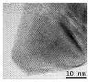
- 238000002173 high-resolution transmission electron microscopy Methods 0.000 description 6
- 229910052738 indium Inorganic materials 0.000 description 6
- 229910052750 molybdenum Inorganic materials 0.000 description 6
- 239000011733 molybdenum Substances 0.000 description 6
- 239000000047 product Substances 0.000 description 6
- 239000011734 sodium Substances 0.000 description 6
- 229910052725 zinc Inorganic materials 0.000 description 6
- 239000011787 zinc oxide Substances 0.000 description 6
- DAFHKNAQFPVRKR-UHFFFAOYSA-N (3-hydroxy-2,2,4-trimethylpentyl) 2-methylpropanoate Chemical compound CC(C)C(O)C(C)(C)COC(=O)C(C)C DAFHKNAQFPVRKR-UHFFFAOYSA-N 0.000 description 5
- BUGBHKTXTAQXES-UHFFFAOYSA-N Selenium Chemical compound [Se] BUGBHKTXTAQXES-UHFFFAOYSA-N 0.000 description 5
- 229910005642 SnTe Inorganic materials 0.000 description 5
- 229910052793 cadmium Inorganic materials 0.000 description 5
- 239000004020 conductor Substances 0.000 description 5
- 239000006185 dispersion Substances 0.000 description 5
- 229910052732 germanium Inorganic materials 0.000 description 5
- 230000003287 optical effect Effects 0.000 description 5
- 238000000926 separation method Methods 0.000 description 5
- 229910052710 silicon Inorganic materials 0.000 description 5
- 238000000235 small-angle X-ray scattering Methods 0.000 description 5
- 239000005361 soda-lime glass Substances 0.000 description 5
- 238000005507 spraying Methods 0.000 description 5
- 238000004544 sputter deposition Methods 0.000 description 5
- 238000005406 washing Methods 0.000 description 5
- BSKHPKMHTQYZBB-UHFFFAOYSA-N 2-methylpyridine Chemical compound CC1=CC=CC=N1 BSKHPKMHTQYZBB-UHFFFAOYSA-N 0.000 description 4
- ITQTTZVARXURQS-UHFFFAOYSA-N 3-methylpyridine Chemical compound CC1=CC=CN=C1 ITQTTZVARXURQS-UHFFFAOYSA-N 0.000 description 4
- KCXVZYZYPLLWCC-UHFFFAOYSA-N EDTA Chemical compound OC(=O)CN(CC(O)=O)CCN(CC(O)=O)CC(O)=O KCXVZYZYPLLWCC-UHFFFAOYSA-N 0.000 description 4
- PIICEJLVQHRZGT-UHFFFAOYSA-N Ethylenediamine Chemical compound NCCN PIICEJLVQHRZGT-UHFFFAOYSA-N 0.000 description 4
- WYURNTSHIVDZCO-UHFFFAOYSA-N Tetrahydrofuran Chemical compound C1CCOC1 WYURNTSHIVDZCO-UHFFFAOYSA-N 0.000 description 4
- 238000002056 X-ray absorption spectroscopy Methods 0.000 description 4
- ITBPIKUGMIZTJR-UHFFFAOYSA-N [bis(hydroxymethyl)amino]methanol Chemical compound OCN(CO)CO ITBPIKUGMIZTJR-UHFFFAOYSA-N 0.000 description 4
- 239000002253 acid Substances 0.000 description 4
- 229910052782 aluminium Inorganic materials 0.000 description 4
- 238000000149 argon plasma sintering Methods 0.000 description 4
- 230000008901 benefit Effects 0.000 description 4
- 230000002902 bimodal effect Effects 0.000 description 4
- ZBCBWPMODOFKDW-UHFFFAOYSA-N diethanolamine Chemical compound OCCNCCO ZBCBWPMODOFKDW-UHFFFAOYSA-N 0.000 description 4
- DNJIEGIFACGWOD-UHFFFAOYSA-N ethyl mercaptane Natural products CCS DNJIEGIFACGWOD-UHFFFAOYSA-N 0.000 description 4
- 150000002500 ions Chemical class 0.000 description 4
- 238000004519 manufacturing process Methods 0.000 description 4
- 229920000642 polymer Polymers 0.000 description 4
- 229920000036 polyvinylpyrrolidone Polymers 0.000 description 4
- 235000013855 polyvinylpyrrolidone Nutrition 0.000 description 4
- 238000002360 preparation method Methods 0.000 description 4
- UMJSCPRVCHMLSP-UHFFFAOYSA-N pyridine Natural products COC1=CC=CN=C1 UMJSCPRVCHMLSP-UHFFFAOYSA-N 0.000 description 4
- 239000010453 quartz Substances 0.000 description 4
- VYPSYNLAJGMNEJ-UHFFFAOYSA-N silicon dioxide Inorganic materials O=[Si]=O VYPSYNLAJGMNEJ-UHFFFAOYSA-N 0.000 description 4
- 229910052714 tellurium Inorganic materials 0.000 description 4
- HPGGPRDJHPYFRM-UHFFFAOYSA-J tin(iv) chloride Chemical compound Cl[Sn](Cl)(Cl)Cl HPGGPRDJHPYFRM-UHFFFAOYSA-J 0.000 description 4
- WRIDQFICGBMAFQ-UHFFFAOYSA-N (E)-8-Octadecenoic acid Natural products CCCCCCCCCC=CCCCCCCC(O)=O WRIDQFICGBMAFQ-UHFFFAOYSA-N 0.000 description 3
- WUOACPNHFRMFPN-SECBINFHSA-N (S)-(-)-alpha-terpineol Chemical compound CC1=CC[C@@H](C(C)(C)O)CC1 WUOACPNHFRMFPN-SECBINFHSA-N 0.000 description 3
- QGLWBTPVKHMVHM-KTKRTIGZSA-N (z)-octadec-9-en-1-amine Chemical compound CCCCCCCC\C=C/CCCCCCCCN QGLWBTPVKHMVHM-KTKRTIGZSA-N 0.000 description 3
- RFFLAFLAYFXFSW-UHFFFAOYSA-N 1,2-dichlorobenzene Chemical compound ClC1=CC=CC=C1Cl RFFLAFLAYFXFSW-UHFFFAOYSA-N 0.000 description 3
- PAWQVTBBRAZDMG-UHFFFAOYSA-N 2-(3-bromo-2-fluorophenyl)acetic acid Chemical compound OC(=O)CC1=CC=CC(Br)=C1F PAWQVTBBRAZDMG-UHFFFAOYSA-N 0.000 description 3
- LQJBNNIYVWPHFW-UHFFFAOYSA-N 20:1omega9c fatty acid Natural products CCCCCCCCCCC=CCCCCCCCC(O)=O LQJBNNIYVWPHFW-UHFFFAOYSA-N 0.000 description 3
- QSBYPNXLFMSGKH-UHFFFAOYSA-N 9-Heptadecensaeure Natural products CCCCCCCC=CCCCCCCCC(O)=O QSBYPNXLFMSGKH-UHFFFAOYSA-N 0.000 description 3
- YMWUJEATGCHHMB-UHFFFAOYSA-N Dichloromethane Chemical compound ClCCl YMWUJEATGCHHMB-UHFFFAOYSA-N 0.000 description 3
- RTZKZFJDLAIYFH-UHFFFAOYSA-N Diethyl ether Chemical compound CCOCC RTZKZFJDLAIYFH-UHFFFAOYSA-N 0.000 description 3
- LFQSCWFLJHTTHZ-UHFFFAOYSA-N Ethanol Chemical compound CCO LFQSCWFLJHTTHZ-UHFFFAOYSA-N 0.000 description 3
- XEKOWRVHYACXOJ-UHFFFAOYSA-N Ethyl acetate Chemical compound CCOC(C)=O XEKOWRVHYACXOJ-UHFFFAOYSA-N 0.000 description 3
- KWYHDKDOAIKMQN-UHFFFAOYSA-N N,N,N',N'-tetramethylethylenediamine Chemical compound CN(C)CCN(C)C KWYHDKDOAIKMQN-UHFFFAOYSA-N 0.000 description 3
- ZMXDDKWLCZADIW-UHFFFAOYSA-N N,N-Dimethylformamide Chemical compound CN(C)C=O ZMXDDKWLCZADIW-UHFFFAOYSA-N 0.000 description 3
- 239000005642 Oleic acid Substances 0.000 description 3
- ZQPPMHVWECSIRJ-UHFFFAOYSA-N Oleic acid Natural products CCCCCCCCC=CCCCCCCCC(O)=O ZQPPMHVWECSIRJ-UHFFFAOYSA-N 0.000 description 3
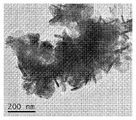
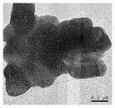
- 238000003917 TEM image Methods 0.000 description 3
- 239000006096 absorbing agent Substances 0.000 description 3
- 150000007513 acids Chemical class 0.000 description 3
- OVKDFILSBMEKLT-UHFFFAOYSA-N alpha-Terpineol Natural products CC(=C)C1(O)CCC(C)=CC1 OVKDFILSBMEKLT-UHFFFAOYSA-N 0.000 description 3
- 230000003667 anti-reflective effect Effects 0.000 description 3
- 238000000231 atomic layer deposition Methods 0.000 description 3
- 229910052799 carbon Inorganic materials 0.000 description 3
- 238000005119 centrifugation Methods 0.000 description 3
- 239000000919 ceramic Substances 0.000 description 3
- OMZSGWSJDCOLKM-UHFFFAOYSA-N copper(II) sulfide Chemical compound [S-2].[Cu+2] OMZSGWSJDCOLKM-UHFFFAOYSA-N 0.000 description 3
- 239000008367 deionised water Substances 0.000 description 3
- 229910021641 deionized water Inorganic materials 0.000 description 3
- 230000008021 deposition Effects 0.000 description 3
- WNAHIZMDSQCWRP-UHFFFAOYSA-N dodecane-1-thiol Chemical compound CCCCCCCCCCCCS WNAHIZMDSQCWRP-UHFFFAOYSA-N 0.000 description 3
- 239000007789 gas Substances 0.000 description 3
- 235000010299 hexamethylene tetramine Nutrition 0.000 description 3
- 239000004312 hexamethylene tetramine Substances 0.000 description 3
- QXJSBBXBKPUZAA-UHFFFAOYSA-N isooleic acid Natural products CCCCCCCC=CCCCCCCCCC(O)=O QXJSBBXBKPUZAA-UHFFFAOYSA-N 0.000 description 3
- VLKZOEOYAKHREP-UHFFFAOYSA-N n-Hexane Chemical compound CCCCCC VLKZOEOYAKHREP-UHFFFAOYSA-N 0.000 description 3
- 239000012299 nitrogen atmosphere Substances 0.000 description 3
- ZQPPMHVWECSIRJ-KTKRTIGZSA-N oleic acid Chemical compound CCCCCCCC\C=C/CCCCCCCC(O)=O ZQPPMHVWECSIRJ-KTKRTIGZSA-N 0.000 description 3
- 238000000634 powder X-ray diffraction Methods 0.000 description 3
- 239000010944 silver (metal) Substances 0.000 description 3
- 239000001509 sodium citrate Substances 0.000 description 3
- 150000003388 sodium compounds Chemical class 0.000 description 3
- 239000002904 solvent Substances 0.000 description 3
- 238000001228 spectrum Methods 0.000 description 3
- 238000010561 standard procedure Methods 0.000 description 3
- 150000004763 sulfides Chemical class 0.000 description 3
- 239000000725 suspension Substances 0.000 description 3
- NWONKYPBYAMBJT-UHFFFAOYSA-L zinc sulfate Chemical compound [Zn+2].[O-]S([O-])(=O)=O NWONKYPBYAMBJT-UHFFFAOYSA-L 0.000 description 3
- 229910000368 zinc sulfate Inorganic materials 0.000 description 3
- 229960001763 zinc sulfate Drugs 0.000 description 3
- RUJPNZNXGCHGID-UHFFFAOYSA-N (Z)-beta-Terpineol Natural products CC(=C)C1CCC(C)(O)CC1 RUJPNZNXGCHGID-UHFFFAOYSA-N 0.000 description 2
- XNWFRZJHXBZDAG-UHFFFAOYSA-N 2-METHOXYETHANOL Chemical compound COCCO XNWFRZJHXBZDAG-UHFFFAOYSA-N 0.000 description 2
- POAOYUHQDCAZBD-UHFFFAOYSA-N 2-butoxyethanol Chemical compound CCCCOCCO POAOYUHQDCAZBD-UHFFFAOYSA-N 0.000 description 2
- ZNQVEEAIQZEUHB-UHFFFAOYSA-N 2-ethoxyethanol Chemical compound CCOCCO ZNQVEEAIQZEUHB-UHFFFAOYSA-N 0.000 description 2
- 229940093475 2-ethoxyethanol Drugs 0.000 description 2
- HWWYDZCSSYKIAD-UHFFFAOYSA-N 3,5-dimethylpyridine Chemical compound CC1=CN=CC(C)=C1 HWWYDZCSSYKIAD-UHFFFAOYSA-N 0.000 description 2
- WHBMMWSBFZVSSR-UHFFFAOYSA-N 3-hydroxybutyric acid Chemical compound CC(O)CC(O)=O WHBMMWSBFZVSSR-UHFFFAOYSA-N 0.000 description 2
- FAXDZWQIWUSWJH-UHFFFAOYSA-N 3-methoxypropan-1-amine Chemical compound COCCCN FAXDZWQIWUSWJH-UHFFFAOYSA-N 0.000 description 2
- OOWFYDWAMOKVSF-UHFFFAOYSA-N 3-methoxypropanenitrile Chemical compound COCCC#N OOWFYDWAMOKVSF-UHFFFAOYSA-N 0.000 description 2
- FBUIIWHYTLCORM-UHFFFAOYSA-N 3-tert-butylpyridine Chemical compound CC(C)(C)C1=CC=CN=C1 FBUIIWHYTLCORM-UHFFFAOYSA-N 0.000 description 2
- OCKGFTQIICXDQW-ZEQRLZLVSA-N 5-[(1r)-1-hydroxy-2-[4-[(2r)-2-hydroxy-2-(4-methyl-1-oxo-3h-2-benzofuran-5-yl)ethyl]piperazin-1-yl]ethyl]-4-methyl-3h-2-benzofuran-1-one Chemical compound C1=C2C(=O)OCC2=C(C)C([C@@H](O)CN2CCN(CC2)C[C@H](O)C2=CC=C3C(=O)OCC3=C2C)=C1 OCKGFTQIICXDQW-ZEQRLZLVSA-N 0.000 description 2
- XKRFYHLGVUSROY-UHFFFAOYSA-N Argon Chemical compound [Ar] XKRFYHLGVUSROY-UHFFFAOYSA-N 0.000 description 2
- HEDRZPFGACZZDS-UHFFFAOYSA-N Chloroform Chemical compound ClC(Cl)Cl HEDRZPFGACZZDS-UHFFFAOYSA-N 0.000 description 2
- 101150023635 Ctse gene Proteins 0.000 description 2
- QUSNBJAOOMFDIB-UHFFFAOYSA-N Ethylamine Chemical compound CCN QUSNBJAOOMFDIB-UHFFFAOYSA-N 0.000 description 2
- VEXZGXHMUGYJMC-UHFFFAOYSA-N Hydrochloric acid Chemical compound Cl VEXZGXHMUGYJMC-UHFFFAOYSA-N 0.000 description 2
- KFZMGEQAYNKOFK-UHFFFAOYSA-N Isopropanol Chemical compound CC(C)O KFZMGEQAYNKOFK-UHFFFAOYSA-N 0.000 description 2
- BAVYZALUXZFZLV-UHFFFAOYSA-N Methylamine Chemical compound NC BAVYZALUXZFZLV-UHFFFAOYSA-N 0.000 description 2
- LRHPLDYGYMQRHN-UHFFFAOYSA-N N-Butanol Chemical compound CCCCO LRHPLDYGYMQRHN-UHFFFAOYSA-N 0.000 description 2
- IMNFDUFMRHMDMM-UHFFFAOYSA-N N-Heptane Chemical compound CCCCCCC IMNFDUFMRHMDMM-UHFFFAOYSA-N 0.000 description 2
- UEEJHVSXFDXPFK-UHFFFAOYSA-N N-dimethylaminoethanol Chemical compound CN(C)CCO UEEJHVSXFDXPFK-UHFFFAOYSA-N 0.000 description 2
- 229920001609 Poly(3,4-ethylenedioxythiophene) Polymers 0.000 description 2
- 238000000833 X-ray absorption fine structure spectroscopy Methods 0.000 description 2
- 238000002441 X-ray diffraction Methods 0.000 description 2
- 238000004833 X-ray photoelectron spectroscopy Methods 0.000 description 2
- 230000002378 acidificating effect Effects 0.000 description 2
- 230000000996 additive effect Effects 0.000 description 2
- 229940088601 alpha-terpineol Drugs 0.000 description 2
- HQABUPZFAYXKJW-UHFFFAOYSA-N butan-1-amine Chemical compound CCCCN HQABUPZFAYXKJW-UHFFFAOYSA-N 0.000 description 2
- OKIIEJOIXGHUKX-UHFFFAOYSA-L cadmium iodide Chemical compound [Cd+2].[I-].[I-] OKIIEJOIXGHUKX-UHFFFAOYSA-L 0.000 description 2
- 239000012159 carrier gas Substances 0.000 description 2
- 230000003197 catalytic effect Effects 0.000 description 2
- 238000000224 chemical solution deposition Methods 0.000 description 2
- 238000005229 chemical vapour deposition Methods 0.000 description 2
- MVPPADPHJFYWMZ-UHFFFAOYSA-N chlorobenzene Chemical compound ClC1=CC=CC=C1 MVPPADPHJFYWMZ-UHFFFAOYSA-N 0.000 description 2
- 229910052804 chromium Inorganic materials 0.000 description 2
- 229920001577 copolymer Polymers 0.000 description 2
- JHIVVAPYMSGYDF-UHFFFAOYSA-N cyclohexanone Chemical compound O=C1CCCCC1 JHIVVAPYMSGYDF-UHFFFAOYSA-N 0.000 description 2
- BGTOWKSIORTVQH-UHFFFAOYSA-N cyclopentanone Chemical compound O=C1CCCC1 BGTOWKSIORTVQH-UHFFFAOYSA-N 0.000 description 2
- 229960002887 deanol Drugs 0.000 description 2
- VTXVGVNLYGSIAR-UHFFFAOYSA-N decane-1-thiol Chemical compound CCCCCCCCCCS VTXVGVNLYGSIAR-UHFFFAOYSA-N 0.000 description 2
- 238000000354 decomposition reaction Methods 0.000 description 2
- 238000000280 densification Methods 0.000 description 2
- 238000003618 dip coating Methods 0.000 description 2
- 238000009713 electroplating Methods 0.000 description 2
- 238000001704 evaporation Methods 0.000 description 2
- 230000008020 evaporation Effects 0.000 description 2
- 230000005669 field effect Effects 0.000 description 2
- NNRLDGQZIVUQTE-UHFFFAOYSA-N gamma-Terpineol Chemical compound CC(C)=C1CCC(C)(O)CC1 NNRLDGQZIVUQTE-UHFFFAOYSA-N 0.000 description 2
- 229910052737 gold Inorganic materials 0.000 description 2
- 150000004679 hydroxides Chemical class 0.000 description 2
- APFVFJFRJDLVQX-UHFFFAOYSA-N indium atom Chemical compound [In] APFVFJFRJDLVQX-UHFFFAOYSA-N 0.000 description 2
- 238000001095 inductively coupled plasma mass spectrometry Methods 0.000 description 2
- XEEYBQQBJWHFJM-UHFFFAOYSA-N iron Substances [Fe] XEEYBQQBJWHFJM-UHFFFAOYSA-N 0.000 description 2
- 229910052742 iron Inorganic materials 0.000 description 2
- 229910052745 lead Inorganic materials 0.000 description 2
- 238000003760 magnetic stirring Methods 0.000 description 2
- 229910021645 metal ion Inorganic materials 0.000 description 2
- 239000002923 metal particle Substances 0.000 description 2
- 239000013081 microcrystal Substances 0.000 description 2
- 239000011859 microparticle Substances 0.000 description 2
- MGFYIUFZLHCRTH-UHFFFAOYSA-N nitrilotriacetic acid Chemical compound OC(=O)CN(CC(O)=O)CC(O)=O MGFYIUFZLHCRTH-UHFFFAOYSA-N 0.000 description 2
- 231100000252 nontoxic Toxicity 0.000 description 2
- 230000003000 nontoxic effect Effects 0.000 description 2
- KZCOBXFFBQJQHH-UHFFFAOYSA-N octane-1-thiol Chemical compound CCCCCCCCS KZCOBXFFBQJQHH-UHFFFAOYSA-N 0.000 description 2
- 239000011368 organic material Substances 0.000 description 2
- 229910052760 oxygen Inorganic materials 0.000 description 2
- XNLICIUVMPYHGG-UHFFFAOYSA-N pentan-2-one Chemical compound CCCC(C)=O XNLICIUVMPYHGG-UHFFFAOYSA-N 0.000 description 2
- 229910052698 phosphorus Inorganic materials 0.000 description 2
- 238000005240 physical vapour deposition Methods 0.000 description 2
- 229920000747 poly(lactic acid) Polymers 0.000 description 2
- 229920001467 poly(styrenesulfonates) Polymers 0.000 description 2
- 229920001223 polyethylene glycol Polymers 0.000 description 2
- 229920001721 polyimide Polymers 0.000 description 2
- 239000001267 polyvinylpyrrolidone Substances 0.000 description 2
- BDERNNFJNOPAEC-UHFFFAOYSA-N propan-1-ol Chemical compound CCCO BDERNNFJNOPAEC-UHFFFAOYSA-N 0.000 description 2
- 239000000376 reactant Substances 0.000 description 2
- NLJMYIDDQXHKNR-UHFFFAOYSA-K sodium citrate Chemical compound O.O.[Na+].[Na+].[Na+].[O-]C(=O)CC(O)(CC([O-])=O)C([O-])=O NLJMYIDDQXHKNR-UHFFFAOYSA-K 0.000 description 2
- 238000003746 solid phase reaction Methods 0.000 description 2
- 238000010671 solid-state reaction Methods 0.000 description 2
- 229910052950 sphalerite Inorganic materials 0.000 description 2
- QJVXKWHHAMZTBY-GCPOEHJPSA-N syringin Chemical compound COC1=CC(\C=C\CO)=CC(OC)=C1O[C@H]1[C@H](O)[C@@H](O)[C@H](O)[C@@H](CO)O1 QJVXKWHHAMZTBY-GCPOEHJPSA-N 0.000 description 2
- PORWMNRCUJJQNO-UHFFFAOYSA-N tellurium atom Chemical compound [Te] PORWMNRCUJJQNO-UHFFFAOYSA-N 0.000 description 2
- YLQBMQCUIZJEEH-UHFFFAOYSA-N tetrahydrofuran Natural products C=1C=COC=1 YLQBMQCUIZJEEH-UHFFFAOYSA-N 0.000 description 2
- 238000004846 x-ray emission Methods 0.000 description 2
- 229910052984 zinc sulfide Inorganic materials 0.000 description 2
- 229910000859 α-Fe Inorganic materials 0.000 description 2
- DGVVWUTYPXICAM-UHFFFAOYSA-N β‐Mercaptoethanol Chemical compound OCCS DGVVWUTYPXICAM-UHFFFAOYSA-N 0.000 description 2
- LZDKZFUFMNSQCJ-UHFFFAOYSA-N 1,2-diethoxyethane Chemical compound CCOCCOCC LZDKZFUFMNSQCJ-UHFFFAOYSA-N 0.000 description 1
- RKDVKSZUMVYZHH-UHFFFAOYSA-N 1,4-dioxane-2,5-dione Chemical compound O=C1COC(=O)CO1 RKDVKSZUMVYZHH-UHFFFAOYSA-N 0.000 description 1
- FXEIVSYQEOJLBU-UHFFFAOYSA-N 1-$l^{1}-selanylethanimine Chemical compound CC([Se])=N FXEIVSYQEOJLBU-UHFFFAOYSA-N 0.000 description 1
- JCVAWLVWQDNEGS-UHFFFAOYSA-N 1-(2-hydroxypropylamino)propan-2-ol;thiolane 1,1-dioxide;hydrate Chemical compound O.O=S1(=O)CCCC1.CC(O)CNCC(C)O JCVAWLVWQDNEGS-UHFFFAOYSA-N 0.000 description 1
- GKWLILHTTGWKLQ-UHFFFAOYSA-N 2,3-dihydrothieno[3,4-b][1,4]dioxine Chemical compound O1CCOC2=CSC=C21 GKWLILHTTGWKLQ-UHFFFAOYSA-N 0.000 description 1
- WUPHOULIZUERAE-UHFFFAOYSA-N 3-(oxolan-2-yl)propanoic acid Chemical compound OC(=O)CCC1CCCO1 WUPHOULIZUERAE-UHFFFAOYSA-N 0.000 description 1
- VHUUQVKOLVNVRT-UHFFFAOYSA-N Ammonium hydroxide Chemical compound [NH4+].[OH-] VHUUQVKOLVNVRT-UHFFFAOYSA-N 0.000 description 1
- DKPFZGUDAPQIHT-UHFFFAOYSA-N Butyl acetate Natural products CCCCOC(C)=O DKPFZGUDAPQIHT-UHFFFAOYSA-N 0.000 description 1
- OKTJSMMVPCPJKN-UHFFFAOYSA-N Carbon Chemical compound [C] OKTJSMMVPCPJKN-UHFFFAOYSA-N 0.000 description 1
- 229910004613 CdTe Inorganic materials 0.000 description 1
- KRKNYBCHXYNGOX-UHFFFAOYSA-K Citrate Chemical compound [O-]C(=O)CC(O)(CC([O-])=O)C([O-])=O KRKNYBCHXYNGOX-UHFFFAOYSA-K 0.000 description 1
- 229910021591 Copper(I) chloride Inorganic materials 0.000 description 1
- 239000004971 Cross linker Substances 0.000 description 1
- XDTMQSROBMDMFD-UHFFFAOYSA-N Cyclohexane Chemical compound C1CCCCC1 XDTMQSROBMDMFD-UHFFFAOYSA-N 0.000 description 1
- XTHFKEDIFFGKHM-UHFFFAOYSA-N Dimethoxyethane Chemical compound COCCOC XTHFKEDIFFGKHM-UHFFFAOYSA-N 0.000 description 1
- KMTRUDSVKNLOMY-UHFFFAOYSA-N Ethylene carbonate Chemical compound O=C1OCCO1 KMTRUDSVKNLOMY-UHFFFAOYSA-N 0.000 description 1
- 239000004606 Fillers/Extenders Substances 0.000 description 1
- DGAQECJNVWCQMB-PUAWFVPOSA-M Ilexoside XXIX Chemical compound C[C@@H]1CC[C@@]2(CC[C@@]3(C(=CC[C@H]4[C@]3(CC[C@@H]5[C@@]4(CC[C@@H](C5(C)C)OS(=O)(=O)[O-])C)C)[C@@H]2[C@]1(C)O)C)C(=O)O[C@H]6[C@@H]([C@H]([C@@H]([C@H](O6)CO)O)O)O.[Na+] DGAQECJNVWCQMB-PUAWFVPOSA-M 0.000 description 1
- 229910021617 Indium monochloride Inorganic materials 0.000 description 1
- NHTMVDHEPJAVLT-UHFFFAOYSA-N Isooctane Chemical compound CC(C)CC(C)(C)C NHTMVDHEPJAVLT-UHFFFAOYSA-N 0.000 description 1
- SECXISVLQFMRJM-UHFFFAOYSA-N N-Methylpyrrolidone Chemical compound CN1CCCC1=O SECXISVLQFMRJM-UHFFFAOYSA-N 0.000 description 1
- 229910002651 NO3 Inorganic materials 0.000 description 1
- NHNBFGGVMKEFGY-UHFFFAOYSA-N Nitrate Chemical compound [O-][N+]([O-])=O NHNBFGGVMKEFGY-UHFFFAOYSA-N 0.000 description 1
- GRYLNZFGIOXLOG-UHFFFAOYSA-N Nitric acid Chemical compound O[N+]([O-])=O GRYLNZFGIOXLOG-UHFFFAOYSA-N 0.000 description 1
- CTQNGGLPUBDAKN-UHFFFAOYSA-N O-Xylene Chemical compound CC1=CC=CC=C1C CTQNGGLPUBDAKN-UHFFFAOYSA-N 0.000 description 1
- 229910019142 PO4 Inorganic materials 0.000 description 1
- OAICVXFJPJFONN-UHFFFAOYSA-N Phosphorus Chemical compound [P] OAICVXFJPJFONN-UHFFFAOYSA-N 0.000 description 1
- 229920001244 Poly(D,L-lactide) Polymers 0.000 description 1
- 229920002845 Poly(methacrylic acid) Polymers 0.000 description 1
- 229920000954 Polyglycolide Polymers 0.000 description 1
- 229920000388 Polyphosphate Polymers 0.000 description 1
- YZCKVEUIGOORGS-IGMARMGPSA-N Protium Chemical compound [1H] YZCKVEUIGOORGS-IGMARMGPSA-N 0.000 description 1
- 229910006404 SnO 2 Inorganic materials 0.000 description 1
- 229910000831 Steel Inorganic materials 0.000 description 1
- 238000004998 X ray absorption near edge structure spectroscopy Methods 0.000 description 1
- ZYQNKFKPTUYGMQ-UHFFFAOYSA-N [In]=[Se].[Zn] Chemical compound [In]=[Se].[Zn] ZYQNKFKPTUYGMQ-UHFFFAOYSA-N 0.000 description 1
- 125000005595 acetylacetonate group Chemical group 0.000 description 1
- 239000002390 adhesive tape Substances 0.000 description 1
- 238000004220 aggregation Methods 0.000 description 1
- 230000002776 aggregation Effects 0.000 description 1
- 238000013019 agitation Methods 0.000 description 1
- 150000001340 alkali metals Chemical class 0.000 description 1
- 150000003973 alkyl amines Chemical class 0.000 description 1
- 150000001356 alkyl thiols Chemical class 0.000 description 1
- XAGFODPZIPBFFR-UHFFFAOYSA-N aluminium Chemical compound [Al] XAGFODPZIPBFFR-UHFFFAOYSA-N 0.000 description 1
- PNEYBMLMFCGWSK-UHFFFAOYSA-N aluminium oxide Inorganic materials [O-2].[O-2].[O-2].[Al+3].[Al+3] PNEYBMLMFCGWSK-UHFFFAOYSA-N 0.000 description 1
- 239000000908 ammonium hydroxide Substances 0.000 description 1
- 229910003481 amorphous carbon Inorganic materials 0.000 description 1
- 239000003963 antioxidant agent Substances 0.000 description 1
- 229910052786 argon Inorganic materials 0.000 description 1
- 238000003491 array Methods 0.000 description 1
- 230000008033 biological extinction Effects 0.000 description 1
- 230000005540 biological transmission Effects 0.000 description 1
- 238000009835 boiling Methods 0.000 description 1
- BDOSMKKIYDKNTQ-UHFFFAOYSA-N cadmium atom Chemical compound [Cd] BDOSMKKIYDKNTQ-UHFFFAOYSA-N 0.000 description 1
- 229940075417 cadmium iodide Drugs 0.000 description 1
- 239000003990 capacitor Substances 0.000 description 1
- 230000015556 catabolic process Effects 0.000 description 1
- 239000003054 catalyst Substances 0.000 description 1
- 150000001768 cations Chemical class 0.000 description 1
- 230000008859 change Effects 0.000 description 1
- 238000010549 co-Evaporation Methods 0.000 description 1
- 230000000536 complexating effect Effects 0.000 description 1
- 229920001940 conductive polymer Polymers 0.000 description 1
- 238000001816 cooling Methods 0.000 description 1
- BWFPGXWASODCHM-UHFFFAOYSA-N copper monosulfide Chemical compound [Cu]=S BWFPGXWASODCHM-UHFFFAOYSA-N 0.000 description 1
- PCRGAMCZHDYVOL-UHFFFAOYSA-N copper selanylidenetin zinc Chemical compound [Cu].[Zn].[Sn]=[Se] PCRGAMCZHDYVOL-UHFFFAOYSA-N 0.000 description 1
- 229910000365 copper sulfate Inorganic materials 0.000 description 1
- OXBLHERUFWYNTN-UHFFFAOYSA-M copper(I) chloride Chemical compound [Cu]Cl OXBLHERUFWYNTN-UHFFFAOYSA-M 0.000 description 1
- ARUVKPQLZAKDPS-UHFFFAOYSA-L copper(II) sulfate Chemical compound [Cu+2].[O-][S+2]([O-])([O-])[O-] ARUVKPQLZAKDPS-UHFFFAOYSA-L 0.000 description 1
- 230000007797 corrosion Effects 0.000 description 1
- 238000005260 corrosion Methods 0.000 description 1
- 238000002447 crystallographic data Methods 0.000 description 1
- XUJNEKJLAYXESH-UHFFFAOYSA-N cysteine Natural products SCC(N)C(O)=O XUJNEKJLAYXESH-UHFFFAOYSA-N 0.000 description 1
- 235000018417 cysteine Nutrition 0.000 description 1
- 238000007405 data analysis Methods 0.000 description 1
- 238000013480 data collection Methods 0.000 description 1
- 238000010908 decantation Methods 0.000 description 1
- 238000006731 degradation reaction Methods 0.000 description 1
- 239000002274 desiccant Substances 0.000 description 1
- 238000001514 detection method Methods 0.000 description 1
- 238000011161 development Methods 0.000 description 1
- 239000003989 dielectric material Substances 0.000 description 1
- 238000010790 dilution Methods 0.000 description 1
- 239000012895 dilution Substances 0.000 description 1
- 238000007598 dipping method Methods 0.000 description 1
- 239000002612 dispersion medium Substances 0.000 description 1
- 238000007606 doctor blade method Methods 0.000 description 1
- 238000004070 electrodeposition Methods 0.000 description 1
- 238000005566 electron beam evaporation Methods 0.000 description 1
- 238000010894 electron beam technology Methods 0.000 description 1
- 239000003995 emulsifying agent Substances 0.000 description 1
- 238000002149 energy-dispersive X-ray emission spectroscopy Methods 0.000 description 1
- 239000000945 filler Substances 0.000 description 1
- 238000001914 filtration Methods 0.000 description 1
- 239000011888 foil Substances 0.000 description 1
- FUZZWVXGSFPDMH-UHFFFAOYSA-N hexanoic acid Chemical compound CCCCCC(O)=O FUZZWVXGSFPDMH-UHFFFAOYSA-N 0.000 description 1
- 125000000487 histidyl group Chemical group [H]N([H])C(C(=O)O*)C([H])([H])C1=C([H])N([H])C([H])=N1 0.000 description 1
- 229920001519 homopolymer Polymers 0.000 description 1
- WQYVRQLZKVEZGA-UHFFFAOYSA-N hypochlorite Chemical class Cl[O-] WQYVRQLZKVEZGA-UHFFFAOYSA-N 0.000 description 1
- 238000010348 incorporation Methods 0.000 description 1
- APHGZSBLRQFRCA-UHFFFAOYSA-M indium(1+);chloride Chemical compound [In]Cl APHGZSBLRQFRCA-UHFFFAOYSA-M 0.000 description 1
- PSCMQHVBLHHWTO-UHFFFAOYSA-K indium(iii) chloride Chemical compound Cl[In](Cl)Cl PSCMQHVBLHHWTO-UHFFFAOYSA-K 0.000 description 1
- AMGQUBHHOARCQH-UHFFFAOYSA-N indium;oxotin Chemical compound [In].[Sn]=O AMGQUBHHOARCQH-UHFFFAOYSA-N 0.000 description 1
- 239000011261 inert gas Substances 0.000 description 1
- 239000003112 inhibitor Substances 0.000 description 1
- 238000007641 inkjet printing Methods 0.000 description 1
- 229910010272 inorganic material Inorganic materials 0.000 description 1
- 239000011147 inorganic material Substances 0.000 description 1
- 239000012212 insulator Substances 0.000 description 1
- 230000003993 interaction Effects 0.000 description 1
- PNHVEGMHOXTHMW-UHFFFAOYSA-N magnesium;zinc;oxygen(2-) Chemical compound [O-2].[O-2].[Mg+2].[Zn+2] PNHVEGMHOXTHMW-UHFFFAOYSA-N 0.000 description 1
- 239000011159 matrix material Substances 0.000 description 1
- 238000005259 measurement Methods 0.000 description 1
- AUHZEENZYGFFBQ-UHFFFAOYSA-N mesitylene Substances CC1=CC(C)=CC(C)=C1 AUHZEENZYGFFBQ-UHFFFAOYSA-N 0.000 description 1
- 125000001827 mesitylenyl group Chemical group [H]C1=C(C(*)=C(C([H])=C1C([H])([H])[H])C([H])([H])[H])C([H])([H])[H] 0.000 description 1
- 150000001247 metal acetylides Chemical class 0.000 description 1
- 229910052976 metal sulfide Inorganic materials 0.000 description 1
- 238000007760 metering rod coating Methods 0.000 description 1
- 125000005395 methacrylic acid group Chemical group 0.000 description 1
- 229930003658 monoterpene Natural products 0.000 description 1
- 150000002773 monoterpene derivatives Chemical class 0.000 description 1
- 235000002577 monoterpenes Nutrition 0.000 description 1
- 230000007935 neutral effect Effects 0.000 description 1
- 150000002823 nitrates Chemical class 0.000 description 1
- 229910017604 nitric acid Inorganic materials 0.000 description 1
- 150000004767 nitrides Chemical class 0.000 description 1
- TVMXDCGIABBOFY-UHFFFAOYSA-N octane Chemical compound CCCCCCCC TVMXDCGIABBOFY-UHFFFAOYSA-N 0.000 description 1
- 239000003960 organic solvent Substances 0.000 description 1
- 150000003891 oxalate salts Chemical class 0.000 description 1
- 230000003647 oxidation Effects 0.000 description 1
- 238000007254 oxidation reaction Methods 0.000 description 1
- MPQXHAGKBWFSNV-UHFFFAOYSA-N oxidophosphanium Chemical class [PH3]=O MPQXHAGKBWFSNV-UHFFFAOYSA-N 0.000 description 1
- AUONHKJOIZSQGR-UHFFFAOYSA-N oxophosphane Chemical compound P=O AUONHKJOIZSQGR-UHFFFAOYSA-N 0.000 description 1
- 239000008188 pellet Substances 0.000 description 1
- VLTRZXGMWDSKGL-UHFFFAOYSA-N perchloric acid Chemical class OCl(=O)(=O)=O VLTRZXGMWDSKGL-UHFFFAOYSA-N 0.000 description 1
- NBIIXXVUZAFLBC-UHFFFAOYSA-K phosphate Chemical compound [O-]P([O-])([O-])=O NBIIXXVUZAFLBC-UHFFFAOYSA-K 0.000 description 1
- 239000010452 phosphate Substances 0.000 description 1
- 239000011574 phosphorus Substances 0.000 description 1
- 229920003023 plastic Polymers 0.000 description 1
- 239000004033 plastic Substances 0.000 description 1
- 239000004014 plasticizer Substances 0.000 description 1
- 229920000768 polyamine Polymers 0.000 description 1
- 229920000515 polycarbonate Polymers 0.000 description 1
- 239000004417 polycarbonate Substances 0.000 description 1
- 229920005646 polycarboxylate Polymers 0.000 description 1
- 229920000570 polyether Polymers 0.000 description 1
- 229920006254 polymer film Polymers 0.000 description 1
- 229920000193 polymethacrylate Polymers 0.000 description 1
- 239000001205 polyphosphate Substances 0.000 description 1
- 235000011176 polyphosphates Nutrition 0.000 description 1
- 229920000379 polypropylene carbonate Polymers 0.000 description 1
- 239000002244 precipitate Substances 0.000 description 1
- 230000002265 prevention Effects 0.000 description 1
- 238000007639 printing Methods 0.000 description 1
- 102000004196 processed proteins & peptides Human genes 0.000 description 1
- 108090000765 processed proteins & peptides Proteins 0.000 description 1
- 238000012545 processing Methods 0.000 description 1
- 238000004549 pulsed laser deposition Methods 0.000 description 1
- 238000000746 purification Methods 0.000 description 1
- 230000005855 radiation Effects 0.000 description 1
- 238000004151 rapid thermal annealing Methods 0.000 description 1
- 230000000717 retained effect Effects 0.000 description 1
- 238000007761 roller coating Methods 0.000 description 1
- 238000007650 screen-printing Methods 0.000 description 1
- SBIBMFFZSBJNJF-UHFFFAOYSA-N selenium;zinc Chemical compound [Se]=[Zn] SBIBMFFZSBJNJF-UHFFFAOYSA-N 0.000 description 1
- 125000004469 siloxy group Chemical group [SiH3]O* 0.000 description 1
- 239000002356 single layer Substances 0.000 description 1
- 238000007764 slot die coating Methods 0.000 description 1
- 229910052708 sodium Inorganic materials 0.000 description 1
- 229910001415 sodium ion Inorganic materials 0.000 description 1
- VPQBLCVGUWPDHV-UHFFFAOYSA-N sodium selenide Chemical compound [Na+].[Na+].[Se-2] VPQBLCVGUWPDHV-UHFFFAOYSA-N 0.000 description 1
- 229910052979 sodium sulfide Inorganic materials 0.000 description 1
- GRVFOGOEDUUMBP-UHFFFAOYSA-N sodium sulfide (anhydrous) Chemical compound [Na+].[Na+].[S-2] GRVFOGOEDUUMBP-UHFFFAOYSA-N 0.000 description 1
- 238000000527 sonication Methods 0.000 description 1
- 238000004528 spin coating Methods 0.000 description 1
- 238000005118 spray pyrolysis Methods 0.000 description 1
- 239000003381 stabilizer Substances 0.000 description 1
- 229910001220 stainless steel Inorganic materials 0.000 description 1
- 239000010935 stainless steel Substances 0.000 description 1
- 229940071182 stannate Drugs 0.000 description 1
- 239000010959 steel Substances 0.000 description 1
- 239000011550 stock solution Substances 0.000 description 1
- QAOWNCQODCNURD-UHFFFAOYSA-L sulfate group Chemical group S(=O)(=O)([O-])[O-] QAOWNCQODCNURD-UHFFFAOYSA-L 0.000 description 1
- 150000003467 sulfuric acid derivatives Chemical class 0.000 description 1
- MLKXDPUZXIRXEP-MFOYZWKCSA-N sulindac Chemical compound CC1=C(CC(O)=O)C2=CC(F)=CC=C2\C1=C/C1=CC=C(S(C)=O)C=C1 MLKXDPUZXIRXEP-MFOYZWKCSA-N 0.000 description 1
- 238000005211 surface analysis Methods 0.000 description 1
- 238000002207 thermal evaporation Methods 0.000 description 1
- 239000002562 thickening agent Substances 0.000 description 1
- 238000002042 time-of-flight secondary ion mass spectrometry Methods 0.000 description 1
- ALRFTTOJSPMYSY-UHFFFAOYSA-N tin disulfide Chemical compound S=[Sn]=S ALRFTTOJSPMYSY-UHFFFAOYSA-N 0.000 description 1
- 230000001988 toxicity Effects 0.000 description 1
- 231100000419 toxicity Toxicity 0.000 description 1
- HRXKRNGNAMMEHJ-UHFFFAOYSA-K trisodium citrate Chemical compound [Na+].[Na+].[Na+].[O-]C(=O)CC(O)(CC([O-])=O)C([O-])=O HRXKRNGNAMMEHJ-UHFFFAOYSA-K 0.000 description 1
- 229940038773 trisodium citrate Drugs 0.000 description 1
- GPRLSGONYQIRFK-MNYXATJNSA-N triton Chemical compound [3H+] GPRLSGONYQIRFK-MNYXATJNSA-N 0.000 description 1
- 229910052721 tungsten Inorganic materials 0.000 description 1
- 238000002491 ultra-small angle X-ray scattering Methods 0.000 description 1
- 229910052720 vanadium Inorganic materials 0.000 description 1
- 238000009736 wetting Methods 0.000 description 1
- 239000008096 xylene Substances 0.000 description 1
- UGZADUVQMDAIAO-UHFFFAOYSA-L zinc hydroxide Chemical compound [OH-].[OH-].[Zn+2] UGZADUVQMDAIAO-UHFFFAOYSA-L 0.000 description 1
- 229910021511 zinc hydroxide Inorganic materials 0.000 description 1
- 229940007718 zinc hydroxide Drugs 0.000 description 1
- RZLVQBNCHSJZPX-UHFFFAOYSA-L zinc sulfate heptahydrate Chemical compound O.O.O.O.O.O.O.[Zn+2].[O-]S([O-])(=O)=O RZLVQBNCHSJZPX-UHFFFAOYSA-L 0.000 description 1
- UQMZPFKLYHOJDL-UHFFFAOYSA-N zinc;cadmium(2+);disulfide Chemical compound [S-2].[S-2].[Zn+2].[Cd+2] UQMZPFKLYHOJDL-UHFFFAOYSA-N 0.000 description 1
- DRDVZXDWVBGGMH-UHFFFAOYSA-N zinc;sulfide Chemical compound [S-2].[Zn+2] DRDVZXDWVBGGMH-UHFFFAOYSA-N 0.000 description 1
Images

Classifications
-
- C—CHEMISTRY; METALLURGY
- C01—INORGANIC CHEMISTRY
- C01G—COMPOUNDS CONTAINING METALS NOT COVERED BY SUBCLASSES C01D OR C01F
- C01G19/00—Compounds of tin
- C01G19/006—Compounds containing tin, with or without oxygen or hydrogen, and containing two or more other elements
-
- B—PERFORMING OPERATIONS; TRANSPORTING
- B82—NANOTECHNOLOGY
- B82B—NANOSTRUCTURES FORMED BY MANIPULATION OF INDIVIDUAL ATOMS, MOLECULES, OR LIMITED COLLECTIONS OF ATOMS OR MOLECULES AS DISCRETE UNITS; MANUFACTURE OR TREATMENT THEREOF
- B82B3/00—Manufacture or treatment of nanostructures by manipulation of individual atoms or molecules, or limited collections of atoms or molecules as discrete units
-
- B—PERFORMING OPERATIONS; TRANSPORTING
- B82—NANOTECHNOLOGY
- B82Y—SPECIFIC USES OR APPLICATIONS OF NANOSTRUCTURES; MEASUREMENT OR ANALYSIS OF NANOSTRUCTURES; MANUFACTURE OR TREATMENT OF NANOSTRUCTURES
- B82Y30/00—Nanotechnology for materials or surface science, e.g. nanocomposites
-
- C—CHEMISTRY; METALLURGY
- C01—INORGANIC CHEMISTRY
- C01B—NON-METALLIC ELEMENTS; COMPOUNDS THEREOF; METALLOIDS OR COMPOUNDS THEREOF NOT COVERED BY SUBCLASS C01C
- C01B17/00—Sulfur; Compounds thereof
-
- C—CHEMISTRY; METALLURGY
- C01—INORGANIC CHEMISTRY
- C01B—NON-METALLIC ELEMENTS; COMPOUNDS THEREOF; METALLOIDS OR COMPOUNDS THEREOF NOT COVERED BY SUBCLASS C01C
- C01B17/00—Sulfur; Compounds thereof
- C01B17/20—Methods for preparing sulfides or polysulfides, in general
-
- C—CHEMISTRY; METALLURGY
- C01—INORGANIC CHEMISTRY
- C01B—NON-METALLIC ELEMENTS; COMPOUNDS THEREOF; METALLOIDS OR COMPOUNDS THEREOF NOT COVERED BY SUBCLASS C01C
- C01B19/00—Selenium; Tellurium; Compounds thereof
- C01B19/002—Compounds containing, besides selenium or tellurium, more than one other element, with -O- and -OH not being considered as anions
-
- C—CHEMISTRY; METALLURGY
- C01—INORGANIC CHEMISTRY
- C01B—NON-METALLIC ELEMENTS; COMPOUNDS THEREOF; METALLOIDS OR COMPOUNDS THEREOF NOT COVERED BY SUBCLASS C01C
- C01B19/00—Selenium; Tellurium; Compounds thereof
- C01B19/007—Tellurides or selenides of metals
-
- C—CHEMISTRY; METALLURGY
- C01—INORGANIC CHEMISTRY
- C01G—COMPOUNDS CONTAINING METALS NOT COVERED BY SUBCLASSES C01D OR C01F
- C01G11/00—Compounds of cadmium
-
- C—CHEMISTRY; METALLURGY
- C01—INORGANIC CHEMISTRY
- C01G—COMPOUNDS CONTAINING METALS NOT COVERED BY SUBCLASSES C01D OR C01F
- C01G3/00—Compounds of copper
-
- C—CHEMISTRY; METALLURGY
- C09—DYES; PAINTS; POLISHES; NATURAL RESINS; ADHESIVES; COMPOSITIONS NOT OTHERWISE PROVIDED FOR; APPLICATIONS OF MATERIALS NOT OTHERWISE PROVIDED FOR
- C09D—COATING COMPOSITIONS, e.g. PAINTS, VARNISHES OR LACQUERS; FILLING PASTES; CHEMICAL PAINT OR INK REMOVERS; INKS; CORRECTING FLUIDS; WOODSTAINS; PASTES OR SOLIDS FOR COLOURING OR PRINTING; USE OF MATERIALS THEREFOR
- C09D11/00—Inks
- C09D11/02—Printing inks
- C09D11/03—Printing inks characterised by features other than the chemical nature of the binder
- C09D11/037—Printing inks characterised by features other than the chemical nature of the binder characterised by the pigment
-
- C—CHEMISTRY; METALLURGY
- C09—DYES; PAINTS; POLISHES; NATURAL RESINS; ADHESIVES; COMPOSITIONS NOT OTHERWISE PROVIDED FOR; APPLICATIONS OF MATERIALS NOT OTHERWISE PROVIDED FOR
- C09D—COATING COMPOSITIONS, e.g. PAINTS, VARNISHES OR LACQUERS; FILLING PASTES; CHEMICAL PAINT OR INK REMOVERS; INKS; CORRECTING FLUIDS; WOODSTAINS; PASTES OR SOLIDS FOR COLOURING OR PRINTING; USE OF MATERIALS THEREFOR
- C09D11/00—Inks
- C09D11/30—Inkjet printing inks
- C09D11/32—Inkjet printing inks characterised by colouring agents
- C09D11/322—Pigment inks
-
- H—ELECTRICITY
- H01—ELECTRIC ELEMENTS
- H01L—SEMICONDUCTOR DEVICES NOT COVERED BY CLASS H10
- H01L21/00—Processes or apparatus adapted for the manufacture or treatment of semiconductor or solid state devices or of parts thereof
- H01L21/02—Manufacture or treatment of semiconductor devices or of parts thereof
- H01L21/02104—Forming layers
- H01L21/02365—Forming inorganic semiconducting materials on a substrate
- H01L21/02518—Deposited layers
- H01L21/02521—Materials
- H01L21/02568—Chalcogenide semiconducting materials not being oxides, e.g. ternary compounds
-
- H—ELECTRICITY
- H01—ELECTRIC ELEMENTS
- H01L—SEMICONDUCTOR DEVICES NOT COVERED BY CLASS H10
- H01L21/00—Processes or apparatus adapted for the manufacture or treatment of semiconductor or solid state devices or of parts thereof
- H01L21/02—Manufacture or treatment of semiconductor devices or of parts thereof
- H01L21/02104—Forming layers
- H01L21/02365—Forming inorganic semiconducting materials on a substrate
- H01L21/02518—Deposited layers
- H01L21/02587—Structure
- H01L21/0259—Microstructure
- H01L21/02601—Nanoparticles
-
- H—ELECTRICITY
- H01—ELECTRIC ELEMENTS
- H01L—SEMICONDUCTOR DEVICES NOT COVERED BY CLASS H10
- H01L21/00—Processes or apparatus adapted for the manufacture or treatment of semiconductor or solid state devices or of parts thereof
- H01L21/02—Manufacture or treatment of semiconductor devices or of parts thereof
- H01L21/02104—Forming layers
- H01L21/02365—Forming inorganic semiconducting materials on a substrate
- H01L21/02612—Formation types
- H01L21/02617—Deposition types
- H01L21/02623—Liquid deposition
- H01L21/02628—Liquid deposition using solutions
-
- H—ELECTRICITY
- H10—SEMICONDUCTOR DEVICES; ELECTRIC SOLID-STATE DEVICES NOT OTHERWISE PROVIDED FOR
- H10F—INORGANIC SEMICONDUCTOR DEVICES SENSITIVE TO INFRARED RADIATION, LIGHT, ELECTROMAGNETIC RADIATION OF SHORTER WAVELENGTH OR CORPUSCULAR RADIATION
- H10F77/00—Constructional details of devices covered by this subclass
- H10F77/10—Semiconductor bodies
- H10F77/12—Active materials
- H10F77/126—Active materials comprising only Group I-III-VI chalcopyrite materials, e.g. CuInSe2, CuGaSe2 or CuInGaSe2 [CIGS]
-
- H—ELECTRICITY
- H10—SEMICONDUCTOR DEVICES; ELECTRIC SOLID-STATE DEVICES NOT OTHERWISE PROVIDED FOR
- H10F—INORGANIC SEMICONDUCTOR DEVICES SENSITIVE TO INFRARED RADIATION, LIGHT, ELECTROMAGNETIC RADIATION OF SHORTER WAVELENGTH OR CORPUSCULAR RADIATION
- H10F77/00—Constructional details of devices covered by this subclass
- H10F77/10—Semiconductor bodies
- H10F77/12—Active materials
- H10F77/128—Active materials comprising only Group I-II-IV-VI kesterite materials, e.g. Cu2ZnSnSe4 or Cu2ZnSnS4
-
- H—ELECTRICITY
- H10—SEMICONDUCTOR DEVICES; ELECTRIC SOLID-STATE DEVICES NOT OTHERWISE PROVIDED FOR
- H10F—INORGANIC SEMICONDUCTOR DEVICES SENSITIVE TO INFRARED RADIATION, LIGHT, ELECTROMAGNETIC RADIATION OF SHORTER WAVELENGTH OR CORPUSCULAR RADIATION
- H10F77/00—Constructional details of devices covered by this subclass
- H10F77/10—Semiconductor bodies
- H10F77/14—Shape of semiconductor bodies; Shapes, relative sizes or dispositions of semiconductor regions within semiconductor bodies
-
- C—CHEMISTRY; METALLURGY
- C01—INORGANIC CHEMISTRY
- C01P—INDEXING SCHEME RELATING TO STRUCTURAL AND PHYSICAL ASPECTS OF SOLID INORGANIC COMPOUNDS
- C01P2004/00—Particle morphology
- C01P2004/01—Particle morphology depicted by an image
- C01P2004/04—Particle morphology depicted by an image obtained by TEM, STEM, STM or AFM
-
- C—CHEMISTRY; METALLURGY
- C01—INORGANIC CHEMISTRY
- C01P—INDEXING SCHEME RELATING TO STRUCTURAL AND PHYSICAL ASPECTS OF SOLID INORGANIC COMPOUNDS
- C01P2004/00—Particle morphology
- C01P2004/60—Particles characterised by their size
- C01P2004/62—Submicrometer sized, i.e. from 0.1-1 micrometer
-
- C—CHEMISTRY; METALLURGY
- C01—INORGANIC CHEMISTRY
- C01P—INDEXING SCHEME RELATING TO STRUCTURAL AND PHYSICAL ASPECTS OF SOLID INORGANIC COMPOUNDS
- C01P2004/00—Particle morphology
- C01P2004/60—Particles characterised by their size
- C01P2004/64—Nanometer sized, i.e. from 1-100 nanometer
-
- C—CHEMISTRY; METALLURGY
- C01—INORGANIC CHEMISTRY
- C01P—INDEXING SCHEME RELATING TO STRUCTURAL AND PHYSICAL ASPECTS OF SOLID INORGANIC COMPOUNDS
- C01P2006/00—Physical properties of inorganic compounds
- C01P2006/40—Electric properties
-
- Y—GENERAL TAGGING OF NEW TECHNOLOGICAL DEVELOPMENTS; GENERAL TAGGING OF CROSS-SECTIONAL TECHNOLOGIES SPANNING OVER SEVERAL SECTIONS OF THE IPC; TECHNICAL SUBJECTS COVERED BY FORMER USPC CROSS-REFERENCE ART COLLECTIONS [XRACs] AND DIGESTS
- Y02—TECHNOLOGIES OR APPLICATIONS FOR MITIGATION OR ADAPTATION AGAINST CLIMATE CHANGE
- Y02E—REDUCTION OF GREENHOUSE GAS [GHG] EMISSIONS, RELATED TO ENERGY GENERATION, TRANSMISSION OR DISTRIBUTION
- Y02E10/00—Energy generation through renewable energy sources
- Y02E10/50—Photovoltaic [PV] energy
- Y02E10/541—CuInSe2 material PV cells
-
- Y—GENERAL TAGGING OF NEW TECHNOLOGICAL DEVELOPMENTS; GENERAL TAGGING OF CROSS-SECTIONAL TECHNOLOGIES SPANNING OVER SEVERAL SECTIONS OF THE IPC; TECHNICAL SUBJECTS COVERED BY FORMER USPC CROSS-REFERENCE ART COLLECTIONS [XRACs] AND DIGESTS
- Y10—TECHNICAL SUBJECTS COVERED BY FORMER USPC
- Y10T—TECHNICAL SUBJECTS COVERED BY FORMER US CLASSIFICATION
- Y10T428/00—Stock material or miscellaneous articles
- Y10T428/23907—Pile or nap type surface or component
- Y10T428/23986—With coating, impregnation, or bond
-
- Y—GENERAL TAGGING OF NEW TECHNOLOGICAL DEVELOPMENTS; GENERAL TAGGING OF CROSS-SECTIONAL TECHNOLOGIES SPANNING OVER SEVERAL SECTIONS OF THE IPC; TECHNICAL SUBJECTS COVERED BY FORMER USPC CROSS-REFERENCE ART COLLECTIONS [XRACs] AND DIGESTS
- Y10—TECHNICAL SUBJECTS COVERED BY FORMER USPC
- Y10T—TECHNICAL SUBJECTS COVERED BY FORMER US CLASSIFICATION
- Y10T428/00—Stock material or miscellaneous articles
- Y10T428/24—Structurally defined web or sheet [e.g., overall dimension, etc.]
- Y10T428/24479—Structurally defined web or sheet [e.g., overall dimension, etc.] including variation in thickness
- Y10T428/24612—Composite web or sheet
-
- Y—GENERAL TAGGING OF NEW TECHNOLOGICAL DEVELOPMENTS; GENERAL TAGGING OF CROSS-SECTIONAL TECHNOLOGIES SPANNING OVER SEVERAL SECTIONS OF THE IPC; TECHNICAL SUBJECTS COVERED BY FORMER USPC CROSS-REFERENCE ART COLLECTIONS [XRACs] AND DIGESTS
- Y10—TECHNICAL SUBJECTS COVERED BY FORMER USPC
- Y10T—TECHNICAL SUBJECTS COVERED BY FORMER US CLASSIFICATION
- Y10T428/00—Stock material or miscellaneous articles
- Y10T428/26—Web or sheet containing structurally defined element or component, the element or component having a specified physical dimension
- Y10T428/268—Monolayer with structurally defined element
Landscapes
- Chemical & Material Sciences (AREA)
- Engineering & Computer Science (AREA)
- Organic Chemistry (AREA)
- Inorganic Chemistry (AREA)
- General Physics & Mathematics (AREA)
- Physics & Mathematics (AREA)
- Nanotechnology (AREA)
- Condensed Matter Physics & Semiconductors (AREA)
- Manufacturing & Machinery (AREA)
- Materials Engineering (AREA)
- Computer Hardware Design (AREA)
- Microelectronics & Electronic Packaging (AREA)
- Power Engineering (AREA)
- Crystallography & Structural Chemistry (AREA)
- Wood Science & Technology (AREA)
- Life Sciences & Earth Sciences (AREA)
- General Chemical & Material Sciences (AREA)
- Chemical Kinetics & Catalysis (AREA)
- Composite Materials (AREA)
- Inks, Pencil-Leads, Or Crayons (AREA)
- Powder Metallurgy (AREA)
- Photovoltaic Devices (AREA)
- Paints Or Removers (AREA)
- Pigments, Carbon Blacks, Or Wood Stains (AREA)
Applications Claiming Priority (10)
| Application Number | Priority Date | Filing Date | Title |
|---|---|---|---|
| US26438909P | 2009-11-25 | 2009-11-25 | |
| US26438709P | 2009-11-25 | 2009-11-25 | |
| US26440409P | 2009-11-25 | 2009-11-25 | |
| US26438309P | 2009-11-25 | 2009-11-25 | |
| US26439309P | 2009-11-25 | 2009-11-25 | |
| US61/264,387 | 2009-11-25 | ||
| US61/264,389 | 2009-11-25 | ||
| US61/264,383 | 2009-11-25 | ||
| US61/264,404 | 2009-11-25 | ||
| US61/264,393 | 2009-11-25 |
Publications (1)
| Publication Number | Publication Date |
|---|---|
| KR20120098799A true KR20120098799A (ko) | 2012-09-05 |
Family
ID=43383645
Family Applications (1)
| Application Number | Title | Priority Date | Filing Date |
|---|---|---|---|
| KR20127016243A Withdrawn KR20120098799A (ko) | 2009-11-25 | 2010-11-22 | 결정형 구리 칼코게나이드 나노입자의 수성 제조 방법, 그렇게 제조된 나노입자, 및 나노입자를 포함하는 잉크 및 코팅된 기재 |
Country Status (6)
| Country | Link |
|---|---|
| US (1) | US8470636B2 (enExample) |
| EP (1) | EP2504276A1 (enExample) |
| JP (1) | JP2013512311A (enExample) |
| KR (1) | KR20120098799A (enExample) |
| CN (1) | CN102612486A (enExample) |
| WO (1) | WO2011066205A1 (enExample) |
Cited By (5)
| Publication number | Priority date | Publication date | Assignee | Title |
|---|---|---|---|---|
| WO2014039937A1 (en) * | 2012-09-07 | 2014-03-13 | Cornell University | Metal chalcogenide synthesis method and applications |
| KR20160041947A (ko) * | 2013-08-09 | 2016-04-18 | 고쿠리츠다이가쿠호진 호쿠리쿠 센단 가가쿠 기쥬츠 다이가쿠인 다이가쿠 | 산화물 반도체층 및 그 제조방법, 그리고 산화물 반도체의 전구체, 산화물 반도체층, 반도체 소자, 및 전자 디바이스 |
| KR20170041091A (ko) * | 2015-10-06 | 2017-04-14 | 삼성전자주식회사 | 금속 칼코게나이드 나노입자 및 그 제조방법 |
| KR101874227B1 (ko) * | 2017-01-18 | 2018-08-02 | 한양대학교 에리카산학협력단 | 구리 칼코지나이드 광 흡수체 및 광 흡수 필름, 및 그들의 제조 방법. |
| KR20190055992A (ko) * | 2017-11-16 | 2019-05-24 | 한국세라믹기술원 | 전이금속 칼코겐화합물을 이용한 전계 효과형 트랜지스터의 제조 방법 |
Families Citing this family (65)
| Publication number | Priority date | Publication date | Assignee | Title |
|---|---|---|---|---|
| US8524524B2 (en) * | 2010-04-22 | 2013-09-03 | General Electric Company | Methods for forming back contact electrodes for cadmium telluride photovoltaic cells |
| FR2964044B1 (fr) * | 2010-08-26 | 2012-09-14 | Commissariat Energie Atomique | Emulsion de metal liquide |
| WO2012075259A1 (en) * | 2010-12-03 | 2012-06-07 | E. I. Du Pont De Nemours And Company | Molecular precursors and processes for preparing copper indium gallium sulfide/selenide coatings and films |
| CN102675960B (zh) * | 2011-03-08 | 2015-08-05 | 深圳市尊业纳米材料有限公司 | 一种纳米铜锡合金导电油墨及其制备方法和使用方法 |
| FR2972443B1 (fr) * | 2011-03-09 | 2016-10-21 | Univ Paul Sabatier - Toulouse Iii (Ups) | Dispersion colloidale d'un materiau a l'etat divise forme de chalcogenure metallique dans un milieu aqueux, materiau a l'etat divise et leurs utilisations |
| US8771555B2 (en) | 2011-05-06 | 2014-07-08 | Neo Solar Power Corp. | Ink composition |
| FR2975223B1 (fr) * | 2011-05-10 | 2016-12-23 | Electricite De France | Traitement thermique par injection d'un gaz caloporteur. |
| JP2012250889A (ja) * | 2011-06-06 | 2012-12-20 | Toyota Motor Corp | 半導体粒子及びその製造方法 |
| JP5687343B2 (ja) * | 2011-06-27 | 2015-03-18 | 京セラ株式会社 | 半導体層の製造方法、光電変換装置の製造方法および半導体原料 |
| US20130037110A1 (en) * | 2011-08-10 | 2013-02-14 | International Business Machines Corporation | Particle-Based Precursor Formation Method and Photovoltaic Device Thereof |
| US9368660B2 (en) * | 2011-08-10 | 2016-06-14 | International Business Machines Corporation | Capping layers for improved crystallization |
| US8551802B2 (en) * | 2011-09-12 | 2013-10-08 | Intermolecular, Inc. | Laser annealing for thin film solar cells |
| JP2013064108A (ja) * | 2011-09-16 | 2013-04-11 | Delsolar Co Ltd | インク組成物及びその形成方法 |
| ES2402313B1 (es) * | 2011-09-30 | 2014-03-04 | Universitat Jaume I De Castellón | Tintas para la obtención "in situ" de calcógenos y/o calcogenuros que dan lugar a capas de semiconductores, su obtención y modo de empleo |
| EP2762444A4 (en) * | 2011-09-30 | 2015-06-10 | Toppan Printing Co Ltd | INK FOR PRODUCING A COMPOSITE THIN-FINISHED LAYER AND PRODUCTION METHOD THEREFOR |
| EP2786419B1 (en) * | 2011-11-30 | 2020-02-12 | Konica Minolta Laboratory U.S.A., Inc. | Method of manufacturing a photovoltaic device |
| US20130217211A1 (en) * | 2012-02-21 | 2013-08-22 | Aqt Solar, Inc. | Controlled-Pressure Process for Production of CZTS Thin-Films |
| US9573809B2 (en) * | 2012-03-30 | 2017-02-21 | Micron Technology, Inc. | Method of forming a metal chalcogenide material and methods of forming memory cells including same |
| EP2647595A2 (en) * | 2012-04-03 | 2013-10-09 | Neo Solar Power Corp. | Ink composition, chalcogenide semiconductor film, photovoltaic device and methods for forming the same |
| WO2013172949A1 (en) * | 2012-05-14 | 2013-11-21 | E. I. Du Pont De Nemours And Company | Dispersible metal chalcogenide nanoparticles |
| EP2870621B1 (en) | 2012-07-09 | 2018-12-26 | Nanoco Technologies, Ltd. | Group 13 selenide nanoparticles |
| US8741688B2 (en) | 2012-07-24 | 2014-06-03 | Micron Technology, Inc. | Methods of forming a metal chalcogenide material |
| FR2993792B1 (fr) * | 2012-07-26 | 2017-09-15 | Imra Europe Sas | Film de chalcogenure(s) metallique(s) cristallise(s) a gros grains, solution colloidale de particules amorphes et procedes de preparation. |
| US8871560B2 (en) * | 2012-08-09 | 2014-10-28 | International Business Machines Corporation | Plasma annealing of thin film solar cells |
| JP6008736B2 (ja) * | 2012-12-26 | 2016-10-19 | 富士フイルム株式会社 | 半導体膜、半導体膜の製造方法、太陽電池、発光ダイオード、薄膜トランジスタおよび電子デバイス |
| KR101960945B1 (ko) * | 2013-03-04 | 2019-03-20 | 나노코 테크놀로지스 리미티드 | 박막 태양 전지를 위한 구리-인듐-갈륨-칼코게나이드 나노 입자 전구체 |
| CN108383090A (zh) * | 2013-03-15 | 2018-08-10 | 纳米技术有限公司 | Cu2XSnY4纳米粒子 |
| KR101716367B1 (ko) * | 2013-03-15 | 2017-03-14 | 나노코 테크놀로지스 리미티드 | Cu2ZnSnS4 나노 입자들 |
| US9634161B2 (en) | 2013-05-01 | 2017-04-25 | Delaware State University | Nanoscale precursors for synthesis of Fe2(Si,Ge)(S,Se)4 crystalline particles and layers |
| US8999746B2 (en) | 2013-08-08 | 2015-04-07 | Tokyo Ohka Kogyo Co., Ltd. | Method of forming metal chalcogenide dispersion, metal chalcogenide dispersion, method of producing light absorbing layer of solar cell, method of producing solar cell |
| WO2015030275A1 (ko) * | 2013-08-30 | 2015-03-05 | 한국에너지기술연구원 | 이성분계 나노입자를 포함하는 슬러리의 숙성 단계가 도입된 ci(g)s계 박막의 제조방법 및 그 방법에 의해 제조된 ci(g)s계 박막 |
| KR101650049B1 (ko) | 2013-09-12 | 2016-08-22 | 주식회사 엘지화학 | 태양전지 광흡수층 제조용 금속 칼코게나이드 나노 입자 및 이의 제조방법 |
| US10170651B2 (en) * | 2014-01-30 | 2019-01-01 | Nanoco Technologies Ltd. | Metal-doped cu(In,Ga) (S,Se)2 nanoparticles |
| CN103803632B (zh) * | 2014-02-28 | 2016-04-06 | 上海海事大学 | 一种碳包覆光热转换纳米材料的制备方法 |
| US10888836B2 (en) * | 2014-07-25 | 2021-01-12 | Chemical and Metal Technologies LLC | Extraction of target materials using CZTS sorbent |
| WO2016053016A1 (ko) * | 2014-09-29 | 2016-04-07 | 이화여자대학교 산학협력단 | CZTSe계 박막 및 이의 제조 방법, 및 상기 CZTSe계 박막을 이용한 태양전지 |
| JP6554332B2 (ja) | 2014-10-30 | 2019-07-31 | 東京応化工業株式会社 | 均一系塗布液及びその製造方法、太陽電池用光吸収層及びその製造方法、並びに太陽電池及びその製造方法 |
| KR102412965B1 (ko) | 2014-12-30 | 2022-06-24 | 삼성전자주식회사 | 2차원 물질층을 포함하는 전자소자 및 잉크젯 프린팅을 이용한 전자소자의 제조방법 |
| US10767112B2 (en) * | 2015-01-15 | 2020-09-08 | The Trustees Of The Columbia University In The City Of New York | Methods of producing metal sulfides, metal selenides, and metal sulfides/selenides having controlled architectures using kinetic control |
| KR101708260B1 (ko) * | 2015-06-18 | 2017-02-20 | 연세대학교 산학협력단 | 전이금속 칼코겐화물 구조체 및 그 제조방법 |
| FR3039531A1 (enExample) * | 2015-07-28 | 2017-02-03 | Nexdot | |
| US10578572B2 (en) | 2016-01-19 | 2020-03-03 | Invensense, Inc. | CMOS integrated microheater for a gas sensor device |
| US11631794B2 (en) | 2016-05-25 | 2023-04-18 | Nippon Shokubai Co., Ltd. | Thermoelectric material, thermoelectric device, powder for thermoelectric material, and method for producing thermoelectric material |
| JP6793087B2 (ja) * | 2016-05-25 | 2020-12-02 | 株式会社日本触媒 | 熱電変換材料、熱電変換素子、熱電変換材料用粉体、及び熱電変換材料の製造方法 |
| CN106025056A (zh) * | 2016-06-12 | 2016-10-12 | 电子科技大学 | 一种锡硫化合物热电材料的制备方法 |
| US10217888B2 (en) * | 2016-10-06 | 2019-02-26 | International Business Machines Corporation | Solution-phase inclusion of silver into chalcogenide semiconductor inks |
| EP3523248A1 (en) * | 2016-10-07 | 2019-08-14 | Haldor Topsøe A/S | KESTERITE MATERIAL OF CZTS, CZTSe OR CZTSSe TYPE |
| CN106505114A (zh) * | 2016-11-03 | 2017-03-15 | 中国科学院兰州化学物理研究所 | 一种铜锡硫光吸收层薄膜材料的制备方法 |
| US10383967B2 (en) | 2016-11-30 | 2019-08-20 | Invensense, Inc. | Substance sensing with tracers |
| CN108383150B (zh) * | 2018-03-01 | 2020-10-30 | 复旦大学 | 一种硫化锌纳米材料的制备方法 |
| CN108249475B (zh) * | 2018-03-01 | 2020-10-30 | 复旦大学 | 一种铜铟硫纳米材料的简易制备方法 |
| WO2019228620A1 (en) * | 2018-05-30 | 2019-12-05 | Toyota Motor Europe | Inks comprising nanoparticles for high-performance inkjet-printed optoelectronics |
| RU2695208C1 (ru) * | 2018-07-17 | 2019-07-22 | Федеральное государственное бюджетное учреждение науки Институт проблем химической физики Российской академии наук (ИПХФ РАН) | Способ получения монозеренных кестеритных порошков |
| RU2718124C1 (ru) * | 2019-06-10 | 2020-03-30 | Федеральное государственное бюджетное учреждение науки Институт проблем химической физики Российской Академии наук (ФГБУН ИПХФ РАН) | Способ получения монозеренных кестеритных порошков из тройных халькогенидов меди и олова и соединений цинка |
| CN113013314B (zh) * | 2019-12-20 | 2022-12-13 | 中国科学院上海硅酸盐研究所 | 一种p型高性能Cu-Sn-S类金刚石结构热电材料及其制备方法 |
| CN115348948B (zh) * | 2020-03-11 | 2024-11-08 | 约翰内斯堡威特沃特斯兰德大学 | 碱金属四元纳米材料 |
| US11492547B2 (en) | 2020-06-04 | 2022-11-08 | UbiQD, Inc. | Low-PH nanoparticles and ligands |
| CN111755323B (zh) * | 2020-07-07 | 2023-07-21 | 内蒙古大学 | 一种铜锌锡硫太阳电池吸收层薄膜的制备方法 |
| CN112142097B (zh) * | 2020-08-31 | 2021-10-29 | 武汉理工大学 | 三水合锡酸镉及其制备方法和应用 |
| CN112279293B (zh) * | 2020-11-02 | 2023-08-25 | 贵州理工学院 | 一种硫化铜纳米材料的制备方法 |
| CN113517370B (zh) * | 2021-06-11 | 2022-10-14 | 上海应用技术大学 | 一种异质构型太阳能电池结构及其制备方法与应用 |
| CN113371754B (zh) * | 2021-06-23 | 2022-06-10 | 石久光学科技发展(北京)有限公司 | 一种高纯度锡酸镉粉体及其制备方法 |
| CN114436318B (zh) * | 2022-01-07 | 2023-10-31 | 安徽师范大学 | 一种水相合成制备单分散Cu2-xS纳米晶的方法 |
| CN114759140B (zh) * | 2022-04-13 | 2025-09-09 | 西北师范大学 | 一种铜锡硫(cts)忆阻器及其制备方法 |
| CN114933327B (zh) * | 2022-06-13 | 2023-12-01 | 佛山(华南)新材料研究院 | 一种制氢材料及其制备方法、应用 |
Family Cites Families (2)
| Publication number | Priority date | Publication date | Assignee | Title |
|---|---|---|---|---|
| FR2921661B1 (fr) * | 2007-10-01 | 2013-05-31 | Centre Nat Rech Scient | Solide hybride organique inorganique a surface modifiee. |
| US20090305449A1 (en) * | 2007-12-06 | 2009-12-10 | Brent Bollman | Methods and Devices For Processing A Precursor Layer In a Group VIA Environment |
-
2010
- 2010-11-22 WO PCT/US2010/057566 patent/WO2011066205A1/en not_active Ceased
- 2010-11-22 US US13/511,699 patent/US8470636B2/en not_active Expired - Fee Related
- 2010-11-22 KR KR20127016243A patent/KR20120098799A/ko not_active Withdrawn
- 2010-11-22 EP EP10787216A patent/EP2504276A1/en not_active Withdrawn
- 2010-11-22 CN CN2010800521136A patent/CN102612486A/zh active Pending
- 2010-11-22 JP JP2012541134A patent/JP2013512311A/ja not_active Withdrawn
Cited By (6)
| Publication number | Priority date | Publication date | Assignee | Title |
|---|---|---|---|---|
| WO2014039937A1 (en) * | 2012-09-07 | 2014-03-13 | Cornell University | Metal chalcogenide synthesis method and applications |
| US10752514B2 (en) | 2012-09-07 | 2020-08-25 | Cornell University | Metal chalcogenide synthesis method and applications |
| KR20160041947A (ko) * | 2013-08-09 | 2016-04-18 | 고쿠리츠다이가쿠호진 호쿠리쿠 센단 가가쿠 기쥬츠 다이가쿠인 다이가쿠 | 산화물 반도체층 및 그 제조방법, 그리고 산화물 반도체의 전구체, 산화물 반도체층, 반도체 소자, 및 전자 디바이스 |
| KR20170041091A (ko) * | 2015-10-06 | 2017-04-14 | 삼성전자주식회사 | 금속 칼코게나이드 나노입자 및 그 제조방법 |
| KR101874227B1 (ko) * | 2017-01-18 | 2018-08-02 | 한양대학교 에리카산학협력단 | 구리 칼코지나이드 광 흡수체 및 광 흡수 필름, 및 그들의 제조 방법. |
| KR20190055992A (ko) * | 2017-11-16 | 2019-05-24 | 한국세라믹기술원 | 전이금속 칼코겐화합물을 이용한 전계 효과형 트랜지스터의 제조 방법 |
Also Published As
| Publication number | Publication date |
|---|---|
| US20120288987A1 (en) | 2012-11-15 |
| WO2011066205A1 (en) | 2011-06-03 |
| CN102612486A (zh) | 2012-07-25 |
| US8470636B2 (en) | 2013-06-25 |
| JP2013512311A (ja) | 2013-04-11 |
| EP2504276A1 (en) | 2012-10-03 |
Similar Documents
| Publication | Publication Date | Title |
|---|---|---|
| US8470636B2 (en) | Aqueous process for producing crystalline copper chalcogenide nanoparticles, the nanoparticles so-produced, and inks and coated substrates incorporating the nanoparticles | |
| US9251922B2 (en) | Preparation of nanoparticle material | |
| US9105796B2 (en) | CZTS/Se precursor inks and methods for preparing CZTS/Se thin films and CZTS/Se-based photovoltaic cells | |
| EP3379585B1 (en) | Preparation of nanoparticle material | |
| US20130221489A1 (en) | Inks and processes to make a chalcogen-containing semiconductor | |
| US20120220066A1 (en) | Czts/se precursor inks and methods for preparing czts/se thin films and czts/se-based photovoltaic cells | |
| KR20140015280A (ko) | 반도체 잉크, 피막, 코팅된 기재 및 제조방법 | |
| US20140220728A1 (en) | Methods of forming semiconductor films including i2-ii-iv-vi4 and i2-(ii,iv)-iv-vi4 semiconductor films and electronic devices including the semiconductor films | |
| US20140048137A1 (en) | Process for preparing coated substrates and photovoltaic devices | |
| JP6688832B2 (ja) | アンチモンがドープされたナノ粒子 | |
| US20140216555A1 (en) | Metal chalcogenides and methods of making and using same | |
| EP2763184A1 (en) | Inks for the in-situ production of chalcogens and/or chalcogenides that form semiconductor layers, production method thereof and use of same | |
| HK1146673B (en) | Preparation of nanoparticle material | |
| HK1146673A (en) | Preparation of nanoparticle material |
Legal Events
| Date | Code | Title | Description |
|---|---|---|---|
| PA0105 | International application |
Patent event date: 20120622 Patent event code: PA01051R01D Comment text: International Patent Application |
|
| PG1501 | Laying open of application | ||
| PC1203 | Withdrawal of no request for examination | ||
| WITN | Application deemed withdrawn, e.g. because no request for examination was filed or no examination fee was paid |