JP2012190865A - 半導体装置の製造方法 - Google Patents
半導体装置の製造方法 Download PDFInfo
- Publication number
- JP2012190865A JP2012190865A JP2011050928A JP2011050928A JP2012190865A JP 2012190865 A JP2012190865 A JP 2012190865A JP 2011050928 A JP2011050928 A JP 2011050928A JP 2011050928 A JP2011050928 A JP 2011050928A JP 2012190865 A JP2012190865 A JP 2012190865A
- Authority
- JP
- Japan
- Prior art keywords
- substrate
- manufacturing
- semiconductor device
- protective film
- silicon carbide
- Prior art date
- Legal status (The legal status is an assumption and is not a legal conclusion. Google has not performed a legal analysis and makes no representation as to the accuracy of the status listed.)
- Granted
Links
Images

Classifications
-
- H—ELECTRICITY
- H10—SEMICONDUCTOR DEVICES; ELECTRIC SOLID-STATE DEVICES NOT OTHERWISE PROVIDED FOR
- H10P—GENERIC PROCESSES OR APPARATUS FOR THE MANUFACTURE OR TREATMENT OF DEVICES COVERED BY CLASS H10
- H10P95/00—Generic processes or apparatus for manufacture or treatments not covered by the other groups of this subclass
- H10P95/90—Thermal treatments, e.g. annealing or sintering
- H10P95/906—Thermal treatments, e.g. annealing or sintering for altering the shape of semiconductors, e.g. smoothing the surface
-
- H—ELECTRICITY
- H10—SEMICONDUCTOR DEVICES; ELECTRIC SOLID-STATE DEVICES NOT OTHERWISE PROVIDED FOR
- H10D—INORGANIC ELECTRIC SEMICONDUCTOR DEVICES
- H10D12/00—Bipolar devices controlled by the field effect, e.g. insulated-gate bipolar transistors [IGBT]
- H10D12/01—Manufacture or treatment
- H10D12/031—Manufacture or treatment of IGBTs
-
- H—ELECTRICITY
- H10—SEMICONDUCTOR DEVICES; ELECTRIC SOLID-STATE DEVICES NOT OTHERWISE PROVIDED FOR
- H10D—INORGANIC ELECTRIC SEMICONDUCTOR DEVICES
- H10D30/00—Field-effect transistors [FET]
- H10D30/01—Manufacture or treatment
- H10D30/021—Manufacture or treatment of FETs having insulated gates [IGFET]
- H10D30/028—Manufacture or treatment of FETs having insulated gates [IGFET] of double-diffused metal oxide semiconductor [DMOS] FETs
- H10D30/0291—Manufacture or treatment of FETs having insulated gates [IGFET] of double-diffused metal oxide semiconductor [DMOS] FETs of vertical DMOS [VDMOS] FETs
-
- H—ELECTRICITY
- H10—SEMICONDUCTOR DEVICES; ELECTRIC SOLID-STATE DEVICES NOT OTHERWISE PROVIDED FOR
- H10D—INORGANIC ELECTRIC SEMICONDUCTOR DEVICES
- H10D30/00—Field-effect transistors [FET]
- H10D30/60—Insulated-gate field-effect transistors [IGFET]
- H10D30/64—Double-diffused metal-oxide semiconductor [DMOS] FETs
- H10D30/66—Vertical DMOS [VDMOS] FETs
-
- H—ELECTRICITY
- H10—SEMICONDUCTOR DEVICES; ELECTRIC SOLID-STATE DEVICES NOT OTHERWISE PROVIDED FOR
- H10D—INORGANIC ELECTRIC SEMICONDUCTOR DEVICES
- H10D62/00—Semiconductor bodies, or regions thereof, of devices having potential barriers
- H10D62/80—Semiconductor bodies, or regions thereof, of devices having potential barriers characterised by the materials
- H10D62/83—Semiconductor bodies, or regions thereof, of devices having potential barriers characterised by the materials being Group IV materials, e.g. B-doped Si or undoped Ge
- H10D62/832—Semiconductor bodies, or regions thereof, of devices having potential barriers characterised by the materials being Group IV materials, e.g. B-doped Si or undoped Ge being Group IV materials comprising two or more elements, e.g. SiGe
- H10D62/8325—Silicon carbide
-
- H—ELECTRICITY
- H10—SEMICONDUCTOR DEVICES; ELECTRIC SOLID-STATE DEVICES NOT OTHERWISE PROVIDED FOR
- H10P—GENERIC PROCESSES OR APPARATUS FOR THE MANUFACTURE OR TREATMENT OF DEVICES COVERED BY CLASS H10
- H10P14/00—Formation of materials, e.g. in the shape of layers or pillars
- H10P14/20—Formation of materials, e.g. in the shape of layers or pillars of semiconductor materials
-
- H—ELECTRICITY
- H10—SEMICONDUCTOR DEVICES; ELECTRIC SOLID-STATE DEVICES NOT OTHERWISE PROVIDED FOR
- H10P—GENERIC PROCESSES OR APPARATUS FOR THE MANUFACTURE OR TREATMENT OF DEVICES COVERED BY CLASS H10
- H10P14/00—Formation of materials, e.g. in the shape of layers or pillars
- H10P14/60—Formation of materials, e.g. in the shape of layers or pillars of insulating materials
- H10P14/63—Formation of materials, e.g. in the shape of layers or pillars of insulating materials characterised by the formation processes
- H10P14/6326—Deposition processes
- H10P14/6349—Deposition of epitaxial materials
-
- H—ELECTRICITY
- H10—SEMICONDUCTOR DEVICES; ELECTRIC SOLID-STATE DEVICES NOT OTHERWISE PROVIDED FOR
- H10P—GENERIC PROCESSES OR APPARATUS FOR THE MANUFACTURE OR TREATMENT OF DEVICES COVERED BY CLASS H10
- H10P30/00—Ion implantation into wafers, substrates or parts of devices
- H10P30/20—Ion implantation into wafers, substrates or parts of devices into semiconductor materials, e.g. for doping
- H10P30/202—Ion implantation into wafers, substrates or parts of devices into semiconductor materials, e.g. for doping characterised by the semiconductor materials
- H10P30/204—Ion implantation into wafers, substrates or parts of devices into semiconductor materials, e.g. for doping characterised by the semiconductor materials into Group IV semiconductors
- H10P30/2042—Ion implantation into wafers, substrates or parts of devices into semiconductor materials, e.g. for doping characterised by the semiconductor materials into Group IV semiconductors into crystalline silicon carbide
-
- H—ELECTRICITY
- H10—SEMICONDUCTOR DEVICES; ELECTRIC SOLID-STATE DEVICES NOT OTHERWISE PROVIDED FOR
- H10P—GENERIC PROCESSES OR APPARATUS FOR THE MANUFACTURE OR TREATMENT OF DEVICES COVERED BY CLASS H10
- H10P30/00—Ion implantation into wafers, substrates or parts of devices
- H10P30/20—Ion implantation into wafers, substrates or parts of devices into semiconductor materials, e.g. for doping
- H10P30/21—Ion implantation into wafers, substrates or parts of devices into semiconductor materials, e.g. for doping of electrically active species
-
- H—ELECTRICITY
- H10—SEMICONDUCTOR DEVICES; ELECTRIC SOLID-STATE DEVICES NOT OTHERWISE PROVIDED FOR
- H10P—GENERIC PROCESSES OR APPARATUS FOR THE MANUFACTURE OR TREATMENT OF DEVICES COVERED BY CLASS H10
- H10P30/00—Ion implantation into wafers, substrates or parts of devices
- H10P30/20—Ion implantation into wafers, substrates or parts of devices into semiconductor materials, e.g. for doping
- H10P30/28—Ion implantation into wafers, substrates or parts of devices into semiconductor materials, e.g. for doping characterised by an annealing step, e.g. for activation of dopants
-
- H—ELECTRICITY
- H10—SEMICONDUCTOR DEVICES; ELECTRIC SOLID-STATE DEVICES NOT OTHERWISE PROVIDED FOR
- H10P—GENERIC PROCESSES OR APPARATUS FOR THE MANUFACTURE OR TREATMENT OF DEVICES COVERED BY CLASS H10
- H10P95/00—Generic processes or apparatus for manufacture or treatments not covered by the other groups of this subclass
- H10P95/90—Thermal treatments, e.g. annealing or sintering
-
- H—ELECTRICITY
- H10—SEMICONDUCTOR DEVICES; ELECTRIC SOLID-STATE DEVICES NOT OTHERWISE PROVIDED FOR
- H10D—INORGANIC ELECTRIC SEMICONDUCTOR DEVICES
- H10D12/00—Bipolar devices controlled by the field effect, e.g. insulated-gate bipolar transistors [IGBT]
- H10D12/01—Manufacture or treatment
- H10D12/031—Manufacture or treatment of IGBTs
- H10D12/032—Manufacture or treatment of IGBTs of vertical IGBTs
Landscapes
- Electrodes Of Semiconductors (AREA)
- Recrystallisation Techniques (AREA)
Abstract
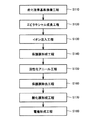
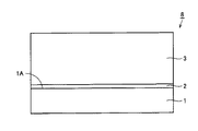
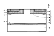
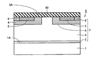
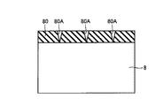
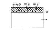
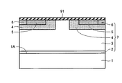
【解決手段】MOSFETの製造方法は、炭化珪素からなるエピタキシャル成長層付き基板8を準備する工程と、エピタキシャル成長層付き基板8にイオン注入を実施する工程と、イオン注入が実施されたエピタキシャル成長層付き基板8上に二酸化珪素からなる保護膜80を形成する工程と、保護膜80が形成されたエピタキシャル成長層付き基板8を、酸素原子を含むガスを含有する雰囲気中において1600℃以上の温度域に加熱する工程とを備えている。
【選択図】図5
Description
Claims (5)
- 炭化珪素からなる基板を準備する工程と、
前記基板にイオン注入を実施する工程と、
前記イオン注入が実施された前記基板上に二酸化珪素からなる保護膜を形成する工程と、
前記保護膜が形成された前記基板を、酸素原子を含むガスを含有する雰囲気中において1600℃以上の温度域に加熱する工程とを備えた、半導体装置の製造方法。 - 前記基板を加熱する工程では、前記保護膜が形成された前記基板が1700℃以下の温度域に加熱される、請求項1に記載の半導体装置の製造方法。
- 前記基板を加熱する工程では、前記保護膜が形成された前記基板が酸素ガスを含有する雰囲気中において加熱される、請求項1または2に記載の半導体装置の製造方法。
- 前記保護膜を形成する工程では、熱酸化により前記保護膜が形成される、請求項1〜3のいずれか1項に記載の半導体装置の製造方法。
- 前記保護膜を形成する工程と前記基板を加熱する工程とは単一の工程として実施される、請求項4に記載の半導体装置の製造方法。
Priority Applications (7)
| Application Number | Priority Date | Filing Date | Title |
|---|---|---|---|
| JP2011050928A JP5659882B2 (ja) | 2011-03-09 | 2011-03-09 | 半導体装置の製造方法 |
| EP11860559.1A EP2685488A4 (en) | 2011-03-09 | 2011-11-15 | METHOD OF MANUFACTURING A SEMICONDUCTOR COMPONENT |
| CN201180067218.3A CN103548118A (zh) | 2011-03-09 | 2011-11-15 | 制造半导体器件的方法 |
| KR1020137018075A KR20140031846A (ko) | 2011-03-09 | 2011-11-15 | 반도체 장치의 제조 방법 |
| PCT/JP2011/076267 WO2012120731A1 (ja) | 2011-03-09 | 2011-11-15 | 半導体装置の製造方法 |
| TW100143597A TW201237968A (en) | 2011-03-09 | 2011-11-28 | Production method for semiconductor device |
| US13/415,406 US8524585B2 (en) | 2011-03-09 | 2012-03-08 | Method of manufacturing semiconductor device |
Applications Claiming Priority (1)
| Application Number | Priority Date | Filing Date | Title |
|---|---|---|---|
| JP2011050928A JP5659882B2 (ja) | 2011-03-09 | 2011-03-09 | 半導体装置の製造方法 |
Publications (3)
| Publication Number | Publication Date |
|---|---|
| JP2012190865A true JP2012190865A (ja) | 2012-10-04 |
| JP2012190865A5 JP2012190865A5 (ja) | 2014-01-23 |
| JP5659882B2 JP5659882B2 (ja) | 2015-01-28 |
Family
ID=46795959
Family Applications (1)
| Application Number | Title | Priority Date | Filing Date |
|---|---|---|---|
| JP2011050928A Expired - Fee Related JP5659882B2 (ja) | 2011-03-09 | 2011-03-09 | 半導体装置の製造方法 |
Country Status (7)
| Country | Link |
|---|---|
| US (1) | US8524585B2 (ja) |
| EP (1) | EP2685488A4 (ja) |
| JP (1) | JP5659882B2 (ja) |
| KR (1) | KR20140031846A (ja) |
| CN (1) | CN103548118A (ja) |
| TW (1) | TW201237968A (ja) |
| WO (1) | WO2012120731A1 (ja) |
Cited By (3)
| Publication number | Priority date | Publication date | Assignee | Title |
|---|---|---|---|---|
| JP2014229708A (ja) * | 2013-05-21 | 2014-12-08 | ローム株式会社 | 半導体装置および半導体装置の製造方法 |
| CN105161416A (zh) * | 2015-09-24 | 2015-12-16 | 株洲南车时代电气股份有限公司 | 一种半导体结构的掺杂方法 |
| JP2017168719A (ja) * | 2016-03-17 | 2017-09-21 | 国立大学法人大阪大学 | 炭化珪素半導体装置の製造方法 |
Families Citing this family (5)
| Publication number | Priority date | Publication date | Assignee | Title |
|---|---|---|---|---|
| CN104143503A (zh) * | 2013-05-07 | 2014-11-12 | 上海凯世通半导体有限公司 | 掺杂方法 |
| JP6314965B2 (ja) * | 2015-12-11 | 2018-04-25 | トヨタ自動車株式会社 | 半導体装置の製造方法 |
| WO2018134024A1 (en) * | 2017-01-17 | 2018-07-26 | Zf Friedrichshafen Ag | Method of manufacturing an insulation layer on silicon carbide |
| CN110391317B (zh) * | 2019-07-29 | 2021-03-09 | 通威太阳能(成都)有限公司 | 一种单晶硅片的绒面制备方法 |
| JP7697313B2 (ja) * | 2021-08-17 | 2025-06-24 | 富士電機株式会社 | 炭化珪素半導体装置および炭化珪素半導体装置の製造方法 |
Citations (4)
| Publication number | Priority date | Publication date | Assignee | Title |
|---|---|---|---|---|
| JPH10125611A (ja) * | 1996-10-17 | 1998-05-15 | Denso Corp | 炭化珪素半導体装置の製造方法 |
| JP2002314071A (ja) * | 2001-04-18 | 2002-10-25 | Denso Corp | 炭化珪素半導体装置の製造方法 |
| JP2010067917A (ja) * | 2008-09-12 | 2010-03-25 | Sumitomo Electric Ind Ltd | 半導体装置の製造方法および半導体装置 |
| JP2010262952A (ja) * | 2009-04-29 | 2010-11-18 | Mitsubishi Electric Corp | 炭化珪素半導体装置の製造方法 |
Family Cites Families (9)
| Publication number | Priority date | Publication date | Assignee | Title |
|---|---|---|---|---|
| US5411907A (en) * | 1992-09-01 | 1995-05-02 | Taiwan Semiconductor Manufacturing Company | Capping free metal silicide integrated process |
| JPH0786199A (ja) | 1993-09-16 | 1995-03-31 | Fuji Electric Co Ltd | 炭化けい素半導体装置の製造方法 |
| KR100327086B1 (ko) * | 1994-06-15 | 2002-03-06 | 구사마 사부로 | 박막 반도체 장치의 제조방법, 박막 반도체 장치,액정표시장치 및 전자기기 |
| US5952679A (en) | 1996-10-17 | 1999-09-14 | Denso Corporation | Semiconductor substrate and method for straightening warp of semiconductor substrate |
| JP3760688B2 (ja) * | 1999-08-26 | 2006-03-29 | 富士電機ホールディングス株式会社 | 炭化けい素半導体素子の製造方法 |
| JP4134575B2 (ja) * | 2002-02-28 | 2008-08-20 | 松下電器産業株式会社 | 半導体装置およびその製造方法 |
| US7572741B2 (en) * | 2005-09-16 | 2009-08-11 | Cree, Inc. | Methods of fabricating oxide layers on silicon carbide layers utilizing atomic oxygen |
| JP5509520B2 (ja) * | 2006-12-21 | 2014-06-04 | 富士電機株式会社 | 炭化珪素半導体装置の製造方法 |
| US7820534B2 (en) * | 2007-08-10 | 2010-10-26 | Mitsubishi Electric Corporation | Method of manufacturing silicon carbide semiconductor device |
-
2011
- 2011-03-09 JP JP2011050928A patent/JP5659882B2/ja not_active Expired - Fee Related
- 2011-11-15 KR KR1020137018075A patent/KR20140031846A/ko not_active Withdrawn
- 2011-11-15 WO PCT/JP2011/076267 patent/WO2012120731A1/ja not_active Ceased
- 2011-11-15 EP EP11860559.1A patent/EP2685488A4/en not_active Withdrawn
- 2011-11-15 CN CN201180067218.3A patent/CN103548118A/zh active Pending
- 2011-11-28 TW TW100143597A patent/TW201237968A/zh unknown
-
2012
- 2012-03-08 US US13/415,406 patent/US8524585B2/en not_active Expired - Fee Related
Patent Citations (4)
| Publication number | Priority date | Publication date | Assignee | Title |
|---|---|---|---|---|
| JPH10125611A (ja) * | 1996-10-17 | 1998-05-15 | Denso Corp | 炭化珪素半導体装置の製造方法 |
| JP2002314071A (ja) * | 2001-04-18 | 2002-10-25 | Denso Corp | 炭化珪素半導体装置の製造方法 |
| JP2010067917A (ja) * | 2008-09-12 | 2010-03-25 | Sumitomo Electric Ind Ltd | 半導体装置の製造方法および半導体装置 |
| JP2010262952A (ja) * | 2009-04-29 | 2010-11-18 | Mitsubishi Electric Corp | 炭化珪素半導体装置の製造方法 |
Cited By (3)
| Publication number | Priority date | Publication date | Assignee | Title |
|---|---|---|---|---|
| JP2014229708A (ja) * | 2013-05-21 | 2014-12-08 | ローム株式会社 | 半導体装置および半導体装置の製造方法 |
| CN105161416A (zh) * | 2015-09-24 | 2015-12-16 | 株洲南车时代电气股份有限公司 | 一种半导体结构的掺杂方法 |
| JP2017168719A (ja) * | 2016-03-17 | 2017-09-21 | 国立大学法人大阪大学 | 炭化珪素半導体装置の製造方法 |
Also Published As
| Publication number | Publication date |
|---|---|
| US8524585B2 (en) | 2013-09-03 |
| KR20140031846A (ko) | 2014-03-13 |
| TW201237968A (en) | 2012-09-16 |
| EP2685488A1 (en) | 2014-01-15 |
| US20120231617A1 (en) | 2012-09-13 |
| EP2685488A4 (en) | 2014-10-22 |
| WO2012120731A1 (ja) | 2012-09-13 |
| CN103548118A (zh) | 2014-01-29 |
| JP5659882B2 (ja) | 2015-01-28 |
Similar Documents
| Publication | Publication Date | Title |
|---|---|---|
| JP5659882B2 (ja) | 半導体装置の製造方法 | |
| JP5141227B2 (ja) | 半導体装置の製造方法 | |
| JP5759293B2 (ja) | 半導体装置の製造方法 | |
| JP2012253108A (ja) | 炭化珪素半導体装置およびその製造方法 | |
| JP2012243966A (ja) | 半導体装置 | |
| JP5626037B2 (ja) | 半導体装置の製造方法 | |
| WO2014046073A1 (ja) | 炭化珪素半導体装置およびその製造方法 | |
| JP5870672B2 (ja) | 半導体装置 | |
| JP2010034481A (ja) | 半導体装置の製造方法および半導体装置 | |
| JP2015191923A (ja) | 炭化珪素半導体装置およびその製造方法 | |
| JP2015204409A (ja) | 炭化珪素半導体装置およびその製造方法 | |
| JP2013172111A (ja) | 炭化珪素半導体装置およびその製造方法 | |
| JP5704003B2 (ja) | 半導体装置の製造方法 | |
| JP5655570B2 (ja) | 半導体装置の製造方法 | |
| JP2016143788A (ja) | 炭化珪素半導体装置の製造方法 | |
| JP2015115570A (ja) | 炭化珪素半導体装置およびその製造方法 | |
| JP2010027638A (ja) | 半導体装置の製造方法および半導体装置 | |
| JP2015115571A (ja) | 炭化珪素半導体装置の製造方法 | |
| JP2015095511A (ja) | 炭化珪素半導体装置およびその製造方法 | |
| JP2017168719A (ja) | 炭化珪素半導体装置の製造方法 |
Legal Events
| Date | Code | Title | Description |
|---|---|---|---|
| A621 | Written request for application examination |
Free format text: JAPANESE INTERMEDIATE CODE: A621 Effective date: 20131029 |
|
| A521 | Request for written amendment filed |
Free format text: JAPANESE INTERMEDIATE CODE: A523 Effective date: 20131204 |
|
| A131 | Notification of reasons for refusal |
Free format text: JAPANESE INTERMEDIATE CODE: A131 Effective date: 20140212 |
|
| A521 | Request for written amendment filed |
Free format text: JAPANESE INTERMEDIATE CODE: A523 Effective date: 20140319 |
|
| TRDD | Decision of grant or rejection written | ||
| A01 | Written decision to grant a patent or to grant a registration (utility model) |
Free format text: JAPANESE INTERMEDIATE CODE: A01 Effective date: 20141104 |
|
| A61 | First payment of annual fees (during grant procedure) |
Free format text: JAPANESE INTERMEDIATE CODE: A61 Effective date: 20141117 |
|
| R150 | Certificate of patent or registration of utility model |
Ref document number: 5659882 Country of ref document: JP Free format text: JAPANESE INTERMEDIATE CODE: R150 |
|
| R250 | Receipt of annual fees |
Free format text: JAPANESE INTERMEDIATE CODE: R250 |
|
| R250 | Receipt of annual fees |
Free format text: JAPANESE INTERMEDIATE CODE: R250 |
|
| R250 | Receipt of annual fees |
Free format text: JAPANESE INTERMEDIATE CODE: R250 |
|
| R250 | Receipt of annual fees |
Free format text: JAPANESE INTERMEDIATE CODE: R250 |
|
| LAPS | Cancellation because of no payment of annual fees |