WO2012120731A1 - 半導体装置の製造方法 - Google Patents
半導体装置の製造方法 Download PDFInfo
- Publication number
- WO2012120731A1 WO2012120731A1 PCT/JP2011/076267 JP2011076267W WO2012120731A1 WO 2012120731 A1 WO2012120731 A1 WO 2012120731A1 JP 2011076267 W JP2011076267 W JP 2011076267W WO 2012120731 A1 WO2012120731 A1 WO 2012120731A1
- Authority
- WO
- WIPO (PCT)
- Prior art keywords
- substrate
- semiconductor device
- protective film
- manufacturing
- region
- Prior art date
Links
- 238000004519 manufacturing process Methods 0.000 title claims abstract description 46
- 239000004065 semiconductor Substances 0.000 title claims description 41
- 239000000758 substrate Substances 0.000 claims abstract description 69
- VYPSYNLAJGMNEJ-UHFFFAOYSA-N Silicium dioxide Chemical compound O=[Si]=O VYPSYNLAJGMNEJ-UHFFFAOYSA-N 0.000 claims abstract description 42
- 230000001681 protective effect Effects 0.000 claims abstract description 37
- HBMJWWWQQXIZIP-UHFFFAOYSA-N silicon carbide Chemical compound [Si+]#[C-] HBMJWWWQQXIZIP-UHFFFAOYSA-N 0.000 claims abstract description 36
- 229910010271 silicon carbide Inorganic materials 0.000 claims abstract description 36
- 239000007789 gas Substances 0.000 claims abstract description 21
- 235000012239 silicon dioxide Nutrition 0.000 claims abstract description 21
- 239000000377 silicon dioxide Substances 0.000 claims abstract description 21
- 238000005468 ion implantation Methods 0.000 claims abstract description 18
- 125000004430 oxygen atom Chemical group O* 0.000 claims abstract description 13
- 238000000034 method Methods 0.000 claims description 25
- 238000010438 heat treatment Methods 0.000 claims description 17
- MYMOFIZGZYHOMD-UHFFFAOYSA-N Dioxygen Chemical compound O=O MYMOFIZGZYHOMD-UHFFFAOYSA-N 0.000 claims description 8
- 229910001882 dioxygen Inorganic materials 0.000 claims description 8
- 230000003647 oxidation Effects 0.000 claims description 4
- 238000007254 oxidation reaction Methods 0.000 claims description 4
- 239000010410 layer Substances 0.000 description 48
- 210000000746 body region Anatomy 0.000 description 21
- 239000012535 impurity Substances 0.000 description 20
- 230000004913 activation Effects 0.000 description 15
- 238000000137 annealing Methods 0.000 description 15
- 230000003746 surface roughness Effects 0.000 description 15
- 239000000463 material Substances 0.000 description 8
- 239000011229 interlayer Substances 0.000 description 7
- XKRFYHLGVUSROY-UHFFFAOYSA-N Argon Chemical compound [Ar] XKRFYHLGVUSROY-UHFFFAOYSA-N 0.000 description 6
- XUIMIQQOPSSXEZ-UHFFFAOYSA-N Silicon Chemical compound [Si] XUIMIQQOPSSXEZ-UHFFFAOYSA-N 0.000 description 6
- PXHVJJICTQNCMI-UHFFFAOYSA-N nickel Substances [Ni] PXHVJJICTQNCMI-UHFFFAOYSA-N 0.000 description 5
- 229910052710 silicon Inorganic materials 0.000 description 5
- 239000010703 silicon Substances 0.000 description 5
- 229910052581 Si3N4 Inorganic materials 0.000 description 4
- 229910004298 SiO 2 Inorganic materials 0.000 description 4
- 238000005229 chemical vapour deposition Methods 0.000 description 4
- 239000004020 conductor Substances 0.000 description 4
- 230000008569 process Effects 0.000 description 4
- HQVNEWCFYHHQES-UHFFFAOYSA-N silicon nitride Chemical compound N12[Si]34N5[Si]62N3[Si]51N64 HQVNEWCFYHHQES-UHFFFAOYSA-N 0.000 description 4
- 229910052786 argon Inorganic materials 0.000 description 3
- 150000002500 ions Chemical class 0.000 description 3
- IJGRMHOSHXDMSA-UHFFFAOYSA-N Atomic nitrogen Chemical compound N#N IJGRMHOSHXDMSA-UHFFFAOYSA-N 0.000 description 2
- KRHYYFGTRYWZRS-UHFFFAOYSA-N Fluorane Chemical compound F KRHYYFGTRYWZRS-UHFFFAOYSA-N 0.000 description 2
- MWUXSHHQAYIFBG-UHFFFAOYSA-N Nitric oxide Chemical compound O=[N] MWUXSHHQAYIFBG-UHFFFAOYSA-N 0.000 description 2
- 230000003213 activating effect Effects 0.000 description 2
- 229910052782 aluminium Inorganic materials 0.000 description 2
- XAGFODPZIPBFFR-UHFFFAOYSA-N aluminium Chemical compound [Al] XAGFODPZIPBFFR-UHFFFAOYSA-N 0.000 description 2
- QVGXLLKOCUKJST-UHFFFAOYSA-N atomic oxygen Chemical compound [O] QVGXLLKOCUKJST-UHFFFAOYSA-N 0.000 description 2
- 230000015556 catabolic process Effects 0.000 description 2
- 238000006243 chemical reaction Methods 0.000 description 2
- 238000005530 etching Methods 0.000 description 2
- 230000005669 field effect Effects 0.000 description 2
- 239000012212 insulator Substances 0.000 description 2
- 239000001301 oxygen Substances 0.000 description 2
- 229910052760 oxygen Inorganic materials 0.000 description 2
- 229910052698 phosphorus Inorganic materials 0.000 description 2
- 238000000206 photolithography Methods 0.000 description 2
- 229910021420 polycrystalline silicon Inorganic materials 0.000 description 2
- 229920005591 polysilicon Polymers 0.000 description 2
- 238000007740 vapor deposition Methods 0.000 description 2
- MGWGWNFMUOTEHG-UHFFFAOYSA-N 4-(3,5-dimethylphenyl)-1,3-thiazol-2-amine Chemical compound CC1=CC(C)=CC(C=2N=C(N)SC=2)=C1 MGWGWNFMUOTEHG-UHFFFAOYSA-N 0.000 description 1
- ZOXJGFHDIHLPTG-UHFFFAOYSA-N Boron Chemical compound [B] ZOXJGFHDIHLPTG-UHFFFAOYSA-N 0.000 description 1
- UGFAIRIUMAVXCW-UHFFFAOYSA-N Carbon monoxide Chemical compound [O+]#[C-] UGFAIRIUMAVXCW-UHFFFAOYSA-N 0.000 description 1
- YCKRFDGAMUMZLT-UHFFFAOYSA-N Fluorine atom Chemical compound [F] YCKRFDGAMUMZLT-UHFFFAOYSA-N 0.000 description 1
- CBENFWSGALASAD-UHFFFAOYSA-N Ozone Chemical compound [O-][O+]=O CBENFWSGALASAD-UHFFFAOYSA-N 0.000 description 1
- OAICVXFJPJFONN-UHFFFAOYSA-N Phosphorus Chemical compound [P] OAICVXFJPJFONN-UHFFFAOYSA-N 0.000 description 1
- 230000002411 adverse Effects 0.000 description 1
- 230000008901 benefit Effects 0.000 description 1
- 229910052796 boron Inorganic materials 0.000 description 1
- 229910002091 carbon monoxide Inorganic materials 0.000 description 1
- 229910052731 fluorine Inorganic materials 0.000 description 1
- 239000011737 fluorine Substances 0.000 description 1
- 239000007788 liquid Substances 0.000 description 1
- 229910044991 metal oxide Inorganic materials 0.000 description 1
- 150000004706 metal oxides Chemical class 0.000 description 1
- 230000004048 modification Effects 0.000 description 1
- 238000012986 modification Methods 0.000 description 1
- 229910052759 nickel Inorganic materials 0.000 description 1
- 229910021334 nickel silicide Inorganic materials 0.000 description 1
- RUFLMLWJRZAWLJ-UHFFFAOYSA-N nickel silicide Chemical compound [Ni]=[Si]=[Ni] RUFLMLWJRZAWLJ-UHFFFAOYSA-N 0.000 description 1
- 229910052757 nitrogen Inorganic materials 0.000 description 1
- JCXJVPUVTGWSNB-UHFFFAOYSA-N nitrogen dioxide Inorganic materials O=[N]=O JCXJVPUVTGWSNB-UHFFFAOYSA-N 0.000 description 1
- 239000011574 phosphorus Substances 0.000 description 1
- 238000005268 plasma chemical vapour deposition Methods 0.000 description 1
- 238000009832 plasma treatment Methods 0.000 description 1
- 238000002360 preparation method Methods 0.000 description 1
- 230000008439 repair process Effects 0.000 description 1
- 238000005092 sublimation method Methods 0.000 description 1
- 230000001629 suppression Effects 0.000 description 1
Images


Classifications
-
- H—ELECTRICITY
- H01—ELECTRIC ELEMENTS
- H01L—SEMICONDUCTOR DEVICES NOT COVERED BY CLASS H10
- H01L21/00—Processes or apparatus adapted for the manufacture or treatment of semiconductor or solid state devices or of parts thereof
- H01L21/02—Manufacture or treatment of semiconductor devices or of parts thereof
- H01L21/04—Manufacture or treatment of semiconductor devices or of parts thereof the devices having at least one potential-jump barrier or surface barrier, e.g. PN junction, depletion layer or carrier concentration layer
- H01L21/18—Manufacture or treatment of semiconductor devices or of parts thereof the devices having at least one potential-jump barrier or surface barrier, e.g. PN junction, depletion layer or carrier concentration layer the devices having semiconductor bodies comprising elements of Group IV of the Periodic System or AIIIBV compounds with or without impurities, e.g. doping materials
- H01L21/30—Treatment of semiconductor bodies using processes or apparatus not provided for in groups H01L21/20 - H01L21/26
- H01L21/324—Thermal treatment for modifying the properties of semiconductor bodies, e.g. annealing, sintering
- H01L21/3247—Thermal treatment for modifying the properties of semiconductor bodies, e.g. annealing, sintering for altering the shape, e.g. smoothing the surface
-
- H—ELECTRICITY
- H01—ELECTRIC ELEMENTS
- H01L—SEMICONDUCTOR DEVICES NOT COVERED BY CLASS H10
- H01L21/00—Processes or apparatus adapted for the manufacture or treatment of semiconductor or solid state devices or of parts thereof
- H01L21/02—Manufacture or treatment of semiconductor devices or of parts thereof
- H01L21/04—Manufacture or treatment of semiconductor devices or of parts thereof the devices having at least one potential-jump barrier or surface barrier, e.g. PN junction, depletion layer or carrier concentration layer
- H01L21/0445—Manufacture or treatment of semiconductor devices or of parts thereof the devices having at least one potential-jump barrier or surface barrier, e.g. PN junction, depletion layer or carrier concentration layer the devices having semiconductor bodies comprising crystalline silicon carbide
- H01L21/0455—Making n or p doped regions or layers, e.g. using diffusion
- H01L21/046—Making n or p doped regions or layers, e.g. using diffusion using ion implantation
-
- H—ELECTRICITY
- H01—ELECTRIC ELEMENTS
- H01L—SEMICONDUCTOR DEVICES NOT COVERED BY CLASS H10
- H01L21/00—Processes or apparatus adapted for the manufacture or treatment of semiconductor or solid state devices or of parts thereof
- H01L21/02—Manufacture or treatment of semiconductor devices or of parts thereof
- H01L21/02104—Forming layers
- H01L21/02107—Forming insulating materials on a substrate
- H01L21/02225—Forming insulating materials on a substrate characterised by the process for the formation of the insulating layer
- H01L21/0226—Forming insulating materials on a substrate characterised by the process for the formation of the insulating layer formation by a deposition process
- H01L21/02293—Forming insulating materials on a substrate characterised by the process for the formation of the insulating layer formation by a deposition process formation of epitaxial layers by a deposition process
-
- H—ELECTRICITY
- H01—ELECTRIC ELEMENTS
- H01L—SEMICONDUCTOR DEVICES NOT COVERED BY CLASS H10
- H01L21/00—Processes or apparatus adapted for the manufacture or treatment of semiconductor or solid state devices or of parts thereof
- H01L21/02—Manufacture or treatment of semiconductor devices or of parts thereof
- H01L21/04—Manufacture or treatment of semiconductor devices or of parts thereof the devices having at least one potential-jump barrier or surface barrier, e.g. PN junction, depletion layer or carrier concentration layer
- H01L21/18—Manufacture or treatment of semiconductor devices or of parts thereof the devices having at least one potential-jump barrier or surface barrier, e.g. PN junction, depletion layer or carrier concentration layer the devices having semiconductor bodies comprising elements of Group IV of the Periodic System or AIIIBV compounds with or without impurities, e.g. doping materials
- H01L21/20—Deposition of semiconductor materials on a substrate, e.g. epitaxial growth solid phase epitaxy
-
- H—ELECTRICITY
- H01—ELECTRIC ELEMENTS
- H01L—SEMICONDUCTOR DEVICES NOT COVERED BY CLASS H10
- H01L21/00—Processes or apparatus adapted for the manufacture or treatment of semiconductor or solid state devices or of parts thereof
- H01L21/02—Manufacture or treatment of semiconductor devices or of parts thereof
- H01L21/04—Manufacture or treatment of semiconductor devices or of parts thereof the devices having at least one potential-jump barrier or surface barrier, e.g. PN junction, depletion layer or carrier concentration layer
- H01L21/18—Manufacture or treatment of semiconductor devices or of parts thereof the devices having at least one potential-jump barrier or surface barrier, e.g. PN junction, depletion layer or carrier concentration layer the devices having semiconductor bodies comprising elements of Group IV of the Periodic System or AIIIBV compounds with or without impurities, e.g. doping materials
- H01L21/30—Treatment of semiconductor bodies using processes or apparatus not provided for in groups H01L21/20 - H01L21/26
- H01L21/324—Thermal treatment for modifying the properties of semiconductor bodies, e.g. annealing, sintering
-
- H—ELECTRICITY
- H01—ELECTRIC ELEMENTS
- H01L—SEMICONDUCTOR DEVICES NOT COVERED BY CLASS H10
- H01L29/00—Semiconductor devices adapted for rectifying, amplifying, oscillating or switching, or capacitors or resistors with at least one potential-jump barrier or surface barrier, e.g. PN junction depletion layer or carrier concentration layer; Details of semiconductor bodies or of electrodes thereof ; Multistep manufacturing processes therefor
- H01L29/66—Types of semiconductor device ; Multistep manufacturing processes therefor
- H01L29/66007—Multistep manufacturing processes
- H01L29/66053—Multistep manufacturing processes of devices having a semiconductor body comprising crystalline silicon carbide
- H01L29/66068—Multistep manufacturing processes of devices having a semiconductor body comprising crystalline silicon carbide the devices being controllable only by the electric current supplied or the electric potential applied, to an electrode which does not carry the current to be rectified, amplified or switched, e.g. three-terminal devices
-
- H—ELECTRICITY
- H01—ELECTRIC ELEMENTS
- H01L—SEMICONDUCTOR DEVICES NOT COVERED BY CLASS H10
- H01L29/00—Semiconductor devices adapted for rectifying, amplifying, oscillating or switching, or capacitors or resistors with at least one potential-jump barrier or surface barrier, e.g. PN junction depletion layer or carrier concentration layer; Details of semiconductor bodies or of electrodes thereof ; Multistep manufacturing processes therefor
- H01L29/66—Types of semiconductor device ; Multistep manufacturing processes therefor
- H01L29/66007—Multistep manufacturing processes
- H01L29/66075—Multistep manufacturing processes of devices having semiconductor bodies comprising group 14 or group 13/15 materials
- H01L29/66227—Multistep manufacturing processes of devices having semiconductor bodies comprising group 14 or group 13/15 materials the devices being controllable only by the electric current supplied or the electric potential applied, to an electrode which does not carry the current to be rectified, amplified or switched, e.g. three-terminal devices
- H01L29/66409—Unipolar field-effect transistors
- H01L29/66477—Unipolar field-effect transistors with an insulated gate, i.e. MISFET
- H01L29/66674—DMOS transistors, i.e. MISFETs with a channel accommodating body or base region adjoining a drain drift region
- H01L29/66712—Vertical DMOS transistors, i.e. VDMOS transistors
-
- H—ELECTRICITY
- H01—ELECTRIC ELEMENTS
- H01L—SEMICONDUCTOR DEVICES NOT COVERED BY CLASS H10
- H01L29/00—Semiconductor devices adapted for rectifying, amplifying, oscillating or switching, or capacitors or resistors with at least one potential-jump barrier or surface barrier, e.g. PN junction depletion layer or carrier concentration layer; Details of semiconductor bodies or of electrodes thereof ; Multistep manufacturing processes therefor
- H01L29/66—Types of semiconductor device ; Multistep manufacturing processes therefor
- H01L29/68—Types of semiconductor device ; Multistep manufacturing processes therefor controllable by only the electric current supplied, or only the electric potential applied, to an electrode which does not carry the current to be rectified, amplified or switched
- H01L29/76—Unipolar devices, e.g. field effect transistors
- H01L29/772—Field effect transistors
- H01L29/78—Field effect transistors with field effect produced by an insulated gate
- H01L29/7801—DMOS transistors, i.e. MISFETs with a channel accommodating body or base region adjoining a drain drift region
- H01L29/7802—Vertical DMOS transistors, i.e. VDMOS transistors
-
- H—ELECTRICITY
- H01—ELECTRIC ELEMENTS
- H01L—SEMICONDUCTOR DEVICES NOT COVERED BY CLASS H10
- H01L29/00—Semiconductor devices adapted for rectifying, amplifying, oscillating or switching, or capacitors or resistors with at least one potential-jump barrier or surface barrier, e.g. PN junction depletion layer or carrier concentration layer; Details of semiconductor bodies or of electrodes thereof ; Multistep manufacturing processes therefor
- H01L29/02—Semiconductor bodies ; Multistep manufacturing processes therefor
- H01L29/12—Semiconductor bodies ; Multistep manufacturing processes therefor characterised by the materials of which they are formed
- H01L29/16—Semiconductor bodies ; Multistep manufacturing processes therefor characterised by the materials of which they are formed including, apart from doping materials or other impurities, only elements of Group IV of the Periodic System
- H01L29/1608—Silicon carbide
Definitions
- the present invention relates to a method for manufacturing a semiconductor device, and more specifically, a method for manufacturing a semiconductor device capable of suppressing surface roughness of a substrate in activation annealing for activating impurities introduced into a substrate made of silicon carbide. It is about.
- silicon carbide has been increasingly adopted as a material constituting semiconductor devices in order to enable higher breakdown voltage, lower loss, and use in high-temperature environments.
- Silicon carbide is a wide band gap semiconductor having a larger band gap than silicon that has been widely used as a material for forming semiconductor devices. Therefore, by adopting silicon carbide as a material constituting the semiconductor device, it is possible to achieve a high breakdown voltage and a low on-resistance of the semiconductor device.
- a semiconductor device that employs silicon carbide as a material has an advantage that a decrease in characteristics when used in a high temperature environment is small as compared with a semiconductor device that employs silicon as a material.
- activation annealing for activating the impurity is performed.
- activation annealing of a substrate made of silicon carbide needs to be performed at a high temperature.
- surface roughness of the substrate may occur due to activation annealing. Since the surface roughness may adversely affect the characteristics of the semiconductor device to be manufactured, it is desirable to reduce the surface roughness.
- a method for manufacturing a silicon carbide semiconductor device has been proposed in which the surface of an ion-implanted region is covered with a silicon nitride film before activation annealing of impurities introduced by ion implantation (for example, JP-A-7-86199 (Patent Document 1)).
- the substrate needs to be heated to a high temperature of 1600 ° C. or higher. Therefore, in the method of manufacturing a semiconductor device described in Patent Document 1, there is a risk that a crack may occur in the silicon nitride film due to a difference in linear expansion coefficient between silicon carbide and silicon nitride. And when a crack arises in the silicon nitride film as a protective film, the problem that the surface roughness of a board
- the present invention has been made to address such problems, and an object thereof is to provide a method of manufacturing a semiconductor device capable of suppressing surface roughness in activation annealing of a substrate made of silicon carbide. That is.
- a method of manufacturing a semiconductor device includes a step of preparing a substrate made of silicon carbide, a step of performing ion implantation on the substrate, and forming a protective film made of silicon dioxide on the substrate on which ion implantation has been performed. And a step of heating the substrate on which the protective film is formed to a temperature range of 1600 ° C. or higher in an atmosphere containing a gas containing oxygen atoms.
- a protective film made of silicon dioxide is formed on a substrate made of silicon carbide on which ion implantation has been performed, and then a temperature of 1600 ° C. or higher in an atmosphere containing a gas containing oxygen atoms.
- Activation annealing is performed by heating the zone.
- the crack is caused by the silicon dioxide generated by the combination of the silicon released from the silicon carbide substrate and the oxygen atoms contained in the gas in the atmosphere. Is suppressed.
- surface roughness in activation annealing of a substrate made of silicon carbide can be suppressed.
- the substrate on which the protective film is formed in the step of heating the substrate, may be heated to a temperature range of 1700 ° C. or lower.
- the heating temperature of the substrate By setting the heating temperature of the substrate to 1700 ° C. or less, it becomes possible to more reliably suppress the surface roughness of the substrate by the protective film made of silicon dioxide.
- the substrate on which the protective film is formed is heated in an atmosphere containing oxygen gas.
- oxygen gas Since oxygen gas is inexpensive and easy to handle, it is suitable as a gas (gas containing oxygen atoms) constituting the atmosphere of the process of heating the substrate.
- the protective film may be formed by thermal oxidation in the step of forming the protective film.
- the protective film made of silicon dioxide can be easily formed.
- the step of forming the protective film and the step of heating the substrate may be performed as a single step.
- the substrate is heated in an atmosphere containing a gas containing oxygen atoms. Therefore, the step of forming the protective film and the step of heating the substrate in an atmosphere containing a gas containing oxygen atoms can be performed as a single step. Thereby, the manufacturing process of the semiconductor device can be simplified.
- the method for manufacturing a semiconductor device of the present invention it is possible to provide a method for manufacturing a semiconductor device capable of suppressing surface roughness in activation annealing of a substrate made of silicon carbide. it can.
- MOSFET Metal Oxide Semiconductor Field Effect Transistor
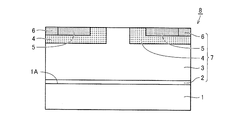
- MOSFET 100 as a semiconductor device is a DiMOSFET, and includes a silicon carbide substrate 1 having a conductivity type of n type (first conductivity type) and a buffer made of silicon carbide and having a conductivity type of n type.
- Layer 2 drift layer 3 made of silicon carbide and having n conductivity type, a pair of p type body regions 4 having conductivity type of p type (second conductivity type), and n + region 5 having conductivity type of n type.
- p + region 6 having a conductivity type of p type.
- Buffer layer 2 is formed on one main surface 1A of silicon carbide substrate 1 and has an n-type conductivity by including an n-type impurity.
- Drift layer 3 is formed on buffer layer 2 and has an n-type conductivity by including an n-type impurity.
- the n-type impurity contained in the drift layer 3 is, for example, N (nitrogen), and is contained at a lower concentration (density) than the n-type impurity contained in the buffer layer 2.
- Buffer layer 2 and drift layer 3 are epitaxial growth layers formed on one main surface 1 ⁇ / b> A of silicon carbide substrate 1.
- the pair of p-type body regions 4 are formed separately from each other so as to include a main surface 3A opposite to the main surface on the silicon carbide substrate 1 side in the epitaxial growth layer, and p-type impurities (conductivity type is p-type). By including an impurity), the conductivity type is p-type.
- the p-type impurity contained in p-type body region 4 is, for example, aluminum (Al), boron (B), or the like.
- the n + region 5 is formed inside each of the pair of p-type body regions 4 so as to include the main surface 3 ⁇ / b > A and be surrounded by the p-type body region 4.
- the n + region 5 contains an n-type impurity, such as P, at a higher concentration (density) than the n-type impurity contained in the drift layer 3.
- P + region 6 includes main surface 3 ⁇ / b > A , is surrounded by p type body region 4, and is formed inside each of the pair of p type body regions 4 so as to be adjacent to n + region 5.
- the p + region 6 contains a p-type impurity such as Al at a higher concentration (density) than the p-type impurity contained in the p-type body region 4.
- the buffer layer 2, the drift layer 3, the p-type body region 4, the n + region 5 and the p + region 6 constitute an active layer 7.
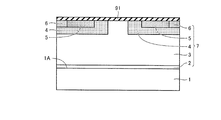
- MOSFET 100 includes a gate oxide film 91 as a gate insulating film, a gate electrode 93, a pair of source contact electrodes 92, an interlayer insulating film 94, a source wiring 95, and a drain electrode 96. And.
- Gate oxide film 91 is formed on main surface 3A of the epitaxial growth layer so as to contact main surface 3A and extend from the upper surface of one n + region 5 to the upper surface of the other n + region 5,
- it is made of silicon dioxide (SiO 2 ).
- Gate electrode 93 is arranged in contact with gate oxide film 91 so as to extend from one n + region 5 to the other n + region 5.
- the gate electrode 93 is made of a conductor such as polysilicon or Al to which impurities are added.
- Source contact electrode 92 extends from each of the pair of n + regions 5 in a direction away from gate oxide film 91 to reach p + region 6 and is in contact with main surface 3A. .
- the source contact electrode 92 is made of a material capable of ohmic contact with the n + region 5 such as Ni x Si y (nickel silicide).
- Interlayer insulating film 94 is formed to surround gate electrode 93 on main surface 3A of drift layer 3 and to extend from one p-type body region 4 to the other p-type body region 4, for example, it is made from silicon dioxide (SiO 2) which is an insulator.
- Source wiring 95 surrounds interlayer insulating film 94 on main surface 3 ⁇ / b> A of drift layer 3 and extends to the upper surface of source contact electrode 92.
- the source wiring 95 is made of a conductor such as Al and is electrically connected to the n + region 5 through the source contact electrode 92.
- Drain electrode 96 is formed in contact with the main surface of silicon carbide substrate 1 opposite to the side on which drift layer 3 is formed. Drain electrode 96 is made of a material capable of making ohmic contact with silicon carbide substrate 1 such as Ni x Si y , and is electrically connected to silicon carbide substrate 1.
- MOSFET 100 in the state where the voltage of gate electrode 93 is lower than the threshold voltage, that is, in the off state, even if a voltage is applied to the drain electrode, p-type body region 4 located immediately below gate oxide film 91 drifts. The pn junction with the layer 3 is reverse-biased and becomes non-conductive.
- a voltage equal to or higher than the threshold voltage is applied to the gate electrode 93, an inversion layer is formed in the channel region in the vicinity of the p-type body region 4 in contact with the gate oxide film 91.
- n + region 5 and drift layer 3 are electrically connected, and a current flows between source line 95 and drain electrode 96.
- MOSFET 100 an inversion layer is formed in the channel region, which is a region in contact with gate oxide film 91 of p-type body region 4, and current flows through the inversion layer. For this reason, when surface roughness occurs on the main surface 3A, the resistance (channel resistance) in the inversion layer increases and the on-resistance increases.
- MOSFET 100 in the present embodiment is manufactured by the method for manufacturing a semiconductor device in the present embodiment described below, so that surface roughness of main surface 3A is reduced and the occurrence of the above problem is suppressed. Yes.
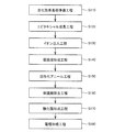
- a method for manufacturing MOSFET 100 in the present embodiment will be described with reference to FIGS.
- a silicon carbide substrate preparation step is performed as a step (S110).
- silicon carbide substrate 1 obtained by slicing an ingot manufactured by a sublimation method is prepared.
- an epitaxial growth step is performed as a step (S120).
- step (S120) referring to FIG. 3, buffer layer 2 and drift layer 3 made of silicon carbide are sequentially formed on one main surface 1A of silicon carbide substrate 1 by epitaxial growth. Thereby, substrate 8 with an epitaxial growth layer as a substrate made of silicon carbide is obtained.
- an ion implantation step is performed as a step (S130).
- step (S130) referring to FIGS. 3 and 4, first, ion implantation for forming p type body region 4 is performed. Specifically, for example, Al (aluminum) ions are implanted into drift layer 3 to form p-type body region 4. Next, ion implantation for forming the n + region 5 is performed. Specifically, for example, P (phosphorus) ions are implanted into p type body region 4 to form n + region 5 in p type body region 4. Further, ion implantation for forming the p + region 6 is performed.
- Al ions are implanted into the p-type body region 4, thereby forming a p + region 6 in the p-type body region 4.
- the ion implantation can be performed by, for example, forming a mask layer made of silicon dioxide (SiO 2 ) on the main surface of the drift layer 3 and having an opening in a desired region where ion implantation is to be performed.
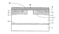
- a protective film forming step is performed as a step (S140).
- protective film 80 made of silicon dioxide is formed on main surface 3A of substrate 8 with the epitaxial growth layer on which ion implantation has been performed in step (S130).
- This protective film 80 can be formed by thermal oxidation, for example.
- the thickness of the protective film 80 can be 0.1 micrometer or more and 1 micrometer or less, for example.
- the protective film 80 may be formed by a CVD method such as plasma CVD (Chemical Vapor Deposition).
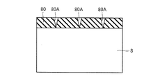
- an activation annealing step is performed as a step (S150).
- the substrate 8 with the epitaxial growth layer on which the protective film 80 is formed in the step (S140) is heated to a temperature range of 1600 ° C. or higher in an atmosphere containing a gas containing oxygen atoms.
- the impurity introduced into the substrate 8 with the epitaxial growth layer by ion implantation in the step (S130) is activated, and the p-type body region 4, n + region 5 and p + region 6 of desired conductivity type are obtained.
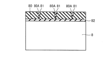
- the substrate 8 with an epitaxial growth layer is heated in an atmosphere containing a gas containing oxygen atoms. Therefore, the silicon separated from the epitaxial growth layer-attached substrate 8 is combined with oxygen in the atmosphere to become silicon dioxide.
- a silicon dioxide film 82 is formed at the boundary between the substrate 8 with the epitaxial growth layer and the protective film 80, and a crack suppressing portion 81 that is made of silicon dioxide and fills (repairs) the crack 80A. Is formed. Thereby, generation
- the gas containing oxygen atoms for example, oxygen gas, ozone gas, nitrogen monoxide gas, nitrogen dioxide gas, carbon monoxide gas and the like can be employed.
- Oxygen gas is particularly suitable as the gas containing oxygen atoms because it is inexpensive and easy to handle.
- the substrate 8 with an epitaxial growth layer may be heated in an oxygen gas atmosphere or an atmosphere containing oxygen gas and argon gas and remaining impurities.
- the heating temperature of the substrate 8 with an epitaxial growth layer is preferably 1700 ° C. or lower.
- the surface roughness can be more reliably suppressed by the protective film 80, the silicon dioxide film 82, and the crack suppressing portion 81 made of silicon dioxide.
- the steps (S140) and (S150) may be performed as a single step.
- the substrate 8 with an epitaxial growth layer is heated to a temperature range of 1100 ° C. or higher and 1600 ° C. or lower for 5 minutes in a reaction chamber containing oxygen gas and argon gas and adjusted to an atmosphere composed of the remaining impurities.
- the heating time is 1600 ° C. or more and 1700 ° C. or less for 1 minute or more and 30 minutes or less in the same reaction chamber without changing the atmosphere.
- Activation annealing is performed by holding.
- the process of manufacturing MOSFET 100 can be simplified by performing steps (S140) and (S150) as a single step.
- a protective film removal step is performed as a step (S160).
- the protective film 80 is removed.
- the removal of the protective film 80 may be performed using, for example, a hydrofluoric acid-based liquid or may be performed by a fluorine-based plasma treatment.
- an oxide film forming step is performed as a step (S170).
- this step (S170) referring to FIG. 8, for example, an oxide film (gate oxide film) 91 is formed by performing a heat treatment of heating to 1300 ° C. and holding for 60 minutes in an oxygen atmosphere.
- an electrode forming step is performed as a step (S180).
- gate electrode 93 made of polysilicon which is a conductor doped with impurities at a high concentration is formed by, for example, CVD, photolithography and etching. Is done.
- an interlayer insulating film 94 made of SiO 2 as an insulator is formed on the main surface 3A so as to surround the gate electrode 93 by, eg, CVD.
- the interlayer insulating film 94 and the oxide film 91 in the region where the source contact electrode 92 is to be formed are removed by photolithography and etching.
- a nickel (Ni) film formed by vapor deposition is heated and silicided, whereby the source contact electrode 92 and the drain electrode 96 are formed.
- source wiring 95 made of Al as a conductor surrounds interlayer insulating film 94 on main surface 3A and extends to the upper surfaces of n + region 5 and source contact electrode 92. To be formed. With the above procedure, MOSFET 100 in the present embodiment is completed.
- the semiconductor device that can be manufactured by the manufacturing method of the present invention is not limited thereto.
- the method of manufacturing a semiconductor device of the present invention can be widely applied to a method of manufacturing a semiconductor device in which a process of performing activation annealing after ion implantation is performed on a substrate made of silicon carbide.
- the method for manufacturing a semiconductor device of the present invention can be applied particularly advantageously to a method for manufacturing a semiconductor device in which a process of performing activation annealing after ion implantation is performed on a substrate made of silicon carbide.
- SYMBOLS 1 Silicon carbide substrate, 1A main surface, 2 Buffer layer, 3 Drift layer, 3A main surface, 4 p-type body area
- 80 Protective film 80A crack, 81 crack suppression portion, 82 silicon dioxide film, 91 gate oxide film (oxide film), 92 source contact electrode, 93 gate electrode, 94 interlayer insulating film, 95 source wiring, 96 drain electrode, 100 MOSFET.
Abstract
MOSFETの製造方法は、炭化珪素からなるエピタキシャル成長層付き基板(8)を準備する工程と、エピタキシャル成長層付き基板(8)にイオン注入を実施する工程と、イオン注入が実施されたエピタキシャル成長層付き基板(8)上に二酸化珪素からなる保護膜(80)を形成する工程と、保護膜(80)が形成されたエピタキシャル成長層付き基板(8)を、酸素原子を含むガスを含有する雰囲気中において1600℃以上の温度域に加熱する工程とを備えている。
Description
本発明は半導体装置の製造方法に関し、より特定的には、炭化珪素からなる基板に導入された不純物を活性化させる活性化アニールにおける基板の表面荒れを抑制することが可能な半導体装置の製造方法に関するものである。
近年、半導体装置の高耐圧化、低損失化、高温環境下での使用などを可能とするため、半導体装置を構成する材料として炭化珪素の採用が進められつつある。炭化珪素は、従来から半導体装置を構成する材料として広く使用されている珪素に比べてバンドギャップが大きいワイドバンドギャップ半導体である。そのため、半導体装置を構成する材料として炭化珪素を採用することにより、半導体装置の高耐圧化、オン抵抗の低減などを達成することができる。また、炭化珪素を材料として採用した半導体装置は、珪素を材料として採用した半導体装置に比べて、高温環境下で使用された場合の特性の低下が小さいという利点も有している。
このような炭化珪素を材料として用いた半導体装置の製造方法では、炭化珪素からなる基板に所望の不純物を導入した後、当該不純物を活性化させる活性化アニールが実施される。ここで、炭化珪素からなる基板の活性化アニールは高温で実施する必要がある。その結果、活性化アニールにより基板の表面荒れが発生する場合がある。この表面荒れは、製造される半導体装置の特性に悪影響を及ぼすおそれがあるため、低減されることが望ましい。
これに対し、イオン注入により導入された不純物の活性化アニールの前に、イオン注入が行なわれた領域の表面を窒化珪素膜により被覆する炭化珪素半導体装置の製造方法が提案されている(たとえば、特開平7-86199号公報(特許文献1)参照)。
しかしながら、上記活性化アニールにおいては、基板は1600℃以上の高温に加熱される必要がある。そのため、上記特許文献1に記載の半導体装置の製造方法では、炭化珪素と窒化珪素との線膨張係数の違い等に起因して、窒化珪素膜に亀裂が生じるおそれがある。そして、保護膜としての窒化珪素膜に亀裂が生じると、基板の表面荒れを十分に抑制できないという問題が生じる。
本発明はこのような問題に対応するためになされたものであって、その目的は、炭化珪素からなる基板の活性化アニールにおける表面荒れを抑制することが可能な半導体装置の製造方法を提供することである。
本発明に従った半導体装置の製造方法は、炭化珪素からなる基板を準備する工程と、基板にイオン注入を実施する工程と、イオン注入が実施された基板上に二酸化珪素からなる保護膜を形成する工程と、保護膜が形成された基板を、酸素原子を含むガスを含有する雰囲気中において1600℃以上の温度域に加熱する工程とを備えている。
本発明の半導体装置の製造方法においては、イオン注入が実施された炭化珪素からなる基板に二酸化珪素からなる保護膜を形成した後、酸素原子を含むガスを含有する雰囲気中において1600℃以上の温度域に加熱することにより活性化アニールが実施される。このとき、二酸化珪素からなる保護膜に亀裂が生じ得る状態となった場合でも、炭化珪素基板から離脱する珪素と雰囲気中のガスに含まれる酸素原子とが結合して生成する二酸化珪素により当該亀裂の発生が抑制される。その結果、本発明の半導体装置の製造方法によれば、炭化珪素からなる基板の活性化アニールにおける表面荒れを抑制することができる。
上記本発明の半導体装置の製造方法においては、基板を加熱する工程では、保護膜が形成された基板が1700℃以下の温度域に加熱されてもよい。基板の加熱温度を1700℃以下とすることにより、二酸化珪素からなる保護膜により基板の表面荒れをより確実に抑制することが可能となる。
上記本発明の半導体装置の製造方法においては、基板を加熱する工程では、保護膜が形成された基板が酸素ガスを含有する雰囲気中において加熱される。
酸素ガスは、安価で取り扱いも容易であるため、上記基板を加熱する工程の雰囲気を構成するガス(酸素原子を含むガス)として好適である。
上記本発明の半導体装置の製造方法においては、保護膜を形成する工程では、熱酸化により保護膜が形成されてもよい。これにより、二酸化珪素からなる保護膜を容易に形成することができる。
上記本発明の半導体装置の製造方法においては、保護膜を形成する工程と基板を加熱する工程とは単一の工程として実施されてもよい。
上記保護膜を熱酸化処理により形成する場合、上記基板は酸素原子を含むガスを含有する雰囲気中において加熱される。そのため、当該保護膜を形成する工程と後続の酸素原子を含むガスを含有する雰囲気中において上記基板を加熱する工程とを単一の工程として実施することができる。これにより、半導体装置の製造プロセスを簡略化することができる。
以上の説明から明らかなように、本発明の半導体装置の製造方法によれば、炭化珪素からなる基板の活性化アニールにおける表面荒れを抑制することが可能な半導体装置の製造方法を提供することができる。
以下、図面に基づいて本発明の実施の形態を説明する。なお、以下の図面において同一または相当する部分には同一の参照番号を付し、その説明は繰返さない。
まず、本発明の一実施の形態における半導体装置の製造方法により製造可能な半導体装置について説明する。図1を参照して、半導体装置としてのMOSFET100は、DiMOSFETであって、導電型がn型(第1導電型)である炭化珪素基板1と、炭化珪素からなり導電型がn型であるバッファ層2と、炭化珪素からなり導電型がn型のドリフト層3と、導電型がp型(第2導電型)の一対のp型ボディ領域4と、導電型がn型のn+領域5と、導電型がp型のp+領域6とを備えている。
バッファ層2は、炭化珪素基板1の一方の主面1A上に形成され、n型不純物を含むことにより導電型がn型となっている。ドリフト層3は、バッファ層2上に形成され、n型不純物を含むことにより導電型がn型となっている。ドリフト層3に含まれるn型不純物は、たとえばN(窒素)であり、バッファ層2に含まれるn型不純物よりも低い濃度(密度)で含まれている。バッファ層2およびドリフト層3は、炭化珪素基板1の一方の主面1A上に形成されたエピタキシャル成長層である。
一対のp型ボディ領域4は、エピタキシャル成長層において、炭化珪素基板1側の主面とは反対側の主面3Aを含むように互いに分離して形成され、p型不純物(導電型がp型である不純物)を含むことにより、導電型がp型となっている。p型ボディ領域4に含まれるp型不純物は、たとえばアルミニウム(Al)、硼素(B)などである。
n+領域5は、上記主面3Aを含み、かつp型ボディ領域4に取り囲まれるように、一対のp型ボディ領域4のそれぞれの内部に形成されている。n+領域5は、n型不純物、たとえばPなどをドリフト層3に含まれるn型不純物よりも高い濃度(密度)で含んでいる。p+領域6は、上記主面3Aを含み、かつp型ボディ領域4に取り囲まれるとともに、n+領域5に隣接するように一対のp型ボディ領域4のそれぞれの内部に形成されている。p+領域6は、p型不純物、たとえばAlなどをp型ボディ領域4に含まれるp型不純物よりも高い濃度(密度)で含んでいる。上記バッファ層2、ドリフト層3、p型ボディ領域4、n+領域5およびp+領域6は、活性層7を構成する。
さらに、図1を参照して、MOSFET100は、ゲート絶縁膜としてのゲート酸化膜91と、ゲート電極93と、一対のソースコンタクト電極92と、層間絶縁膜94と、ソース配線95と、ドレイン電極96とを備えている。
ゲート酸化膜91は、主面3Aに接触し、一方のn+領域5の上部表面から他方のn+領域5の上部表面にまで延在するようにエピタキシャル成長層の主面3A上に形成され、たとえば二酸化珪素(SiO2)からなっている。
ゲート電極93は、一方のn+領域5上から他方のn+領域5上にまで延在するように、ゲート酸化膜91に接触して配置されている。また、ゲート電極93は、不純物が添加されたポリシリコン、Alなどの導電体からなっている。
ソースコンタクト電極92は、一対のn+領域5上のそれぞれから、ゲート酸化膜91から離れる向きに延在してp+領域6上にまで達するとともに、主面3Aに接触して配置されている。また、ソースコンタクト電極92は、たとえばNixSiy(ニッケルシリサイド)など、n+領域5とオーミックコンタクト可能な材料からなっている。
層間絶縁膜94は、ドリフト層3の主面3A上においてゲート電極93を取り囲み、かつ一方のp型ボディ領域4上から他方のp型ボディ領域4上にまで延在するように形成され、たとえば絶縁体である二酸化珪素(SiO2)からなっている。
ソース配線95は、ドリフト層3の主面3A上において、層間絶縁膜94を取り囲み、かつソースコンタクト電極92の上部表面上にまで延在している。また、ソース配線95は、Alなどの導電体からなり、ソースコンタクト電極92を介してn+領域5と電気的に接続されている。
ドレイン電極96は、炭化珪素基板1においてドリフト層3が形成される側とは反対側の主面に接触して形成されている。このドレイン電極96は、たとえばNixSiyなど、炭化珪素基板1とオーミックコンタクト可能な材料からなっており、炭化珪素基板1と電気的に接続されている。
次に、MOSFET100の動作について説明する。図1を参照して、ゲート電極93の電圧が閾値電圧未満の状態、すなわちオフ状態では、ドレイン電極に電圧が印加されても、ゲート酸化膜91の直下に位置するp型ボディ領域4とドリフト層3との間のpn接合が逆バイアスとなり、非導通状態となる。一方、ゲート電極93に閾値電圧以上の電圧を印加すると、p型ボディ領域4のゲート酸化膜91と接触する付近であるチャネル領域において、反転層が形成される。その結果、n+領域5とドリフト層3とが電気的に接続され、ソース配線95とドレイン電極96との間に電流が流れる。
ここで、上述のようにMOSFET100では、p型ボディ領域4のゲート酸化膜91と接触する付近の領域であるチャネル領域において反転層が形成され、当該反転層を電流が流れる。そのため、主面3Aに面荒れが生じた場合、反転層における抵抗(チャネル抵抗)が上昇し、オン抵抗が高くなるという問題を生じ得る。しかし、本実施の形態におけるMOSFET100は、以下に説明する本実施の形態における半導体装置の製造方法により製造されていることにより、主面3Aの面荒れが低減され、上記問題の発生が抑制されている。
次に、本実施の形態におけるMOSFET100の製造方法について、図2~図8を参照して説明する。図2を参照して、本実施の形態におけるMOSFET100の製造方法では、まず工程(S110)として炭化珪素基板準備工程が実施される。この工程(S110)では、図3を参照して、たとえば昇華法により製造されたインゴットをスライスして得られた炭化珪素基板1が準備される。
次に、工程(S120)としてエピタキシャル成長工程が実施される。この工程(S120)では、図3を参照して、エピタキシャル成長により炭化珪素基板1の一方の主面1A上に炭化珪素からなるバッファ層2およびドリフト層3が順次形成される。これにより、炭化珪素からなる基板としてのエピタキシャル成長層付き基板8が得られる。
次に、工程(S130)としてイオン注入工程が実施される。この工程(S130)では、図3および図4を参照して、まずp型ボディ領域4を形成するためのイオン注入が実施される。具体的には、たとえばAl(アルミニウム)イオンがドリフト層3に注入されることにより、p型ボディ領域4が形成される。次に、n+領域5を形成するためのイオン注入が実施される。具体的には、たとえばP(リン)イオンがp型ボディ領域4に注入されることにより、p型ボディ領域4内にn+領域5が形成される。さらに、p+領域6を形成するためのイオン注入が実施される。具体的には、たとえばAlイオンがp型ボディ領域4に注入されることにより、p型ボディ領域4内にp+領域6が形成される。上記イオン注入は、たとえばドリフト層3の主面上に二酸化珪素(SiO2)からなり、イオン注入を実施すべき所望の領域に開口を有するマスク層を形成して実施することができる。
次に、工程(S140)として保護膜形成工程が実施される。この工程(S140)では、図5を参照して、工程(S130)においてイオン注入が実施されたエピタキシャル成長層付き基板8の主面3A上に二酸化珪素からなる保護膜80が形成される。この保護膜80は、たとえば熱酸化により形成することができる。また、保護膜80の厚みは、たとえば0.1μm以上1μm以下とすることができる。保護膜80は、プラズマCVD(Chemical Vapor Deposition)などのCVD法により形成されてもよい。
次に、工程(S150)として活性化アニール工程が実施される。この工程(S150)では、工程(S140)において保護膜80が形成されたエピタキシャル成長層付き基板8が、酸素原子を含むガスを含有する雰囲気中において1600℃以上の温度域に加熱される。これにより、工程(S130)においてイオン注入によりエピタキシャル成長層付き基板8に導入された不純物が活性化し、所望の導電型のp型ボディ領域4、n+領域5およびp+領域6が得られる。
このとき、工程(S150)においてエピタキシャル成長層付き基板8が、たとえばアルゴンガス雰囲気中において加熱された場合、図6に示すように炭化珪素と二酸化珪素との線膨張係数の違い等に起因して保護膜80に亀裂80Aが生じるおそれがある。この場合、エピタキシャル成長層付き基板8から離脱した珪素原子が当該亀裂80Aを通して雰囲気中に放出される。その結果、表面荒れが発生する。
これに対し、本実施の形態における工程(S150)では、エピタキシャル成長層付き基板8が酸素原子を含むガスを含有する雰囲気中において加熱される。そのため、エピタキシャル成長層付き基板8から離脱した珪素は雰囲気中の酸素と結合し、二酸化珪素となる。その結果、図7に示すように、エピタキシャル成長層付き基板8と保護膜80との境界部に二酸化珪素膜82が形成されるとともに、二酸化珪素からなり亀裂80Aを充填(修復)する亀裂抑制部81が形成される。これにより、亀裂80Aの発生や成長が抑制され、表面荒れの発生が低減される。
ここで、上記酸素原子を含むガスとしては、たとえば酸素ガス、オゾンガス、一酸化窒素ガス、二酸化窒素ガス、一酸化炭素ガスなどを採用することができる。酸素ガスは、安価で取り扱いも容易であるため、上記酸素原子を含むガスとして特に好適である。また、工程(S150)では、エピタキシャル成長層付き基板8が、酸素ガス雰囲気中、または酸素ガスとアルゴンガスとを含有し、残部不純物からなる雰囲気中において加熱されてもよい。
また、工程(S150)では、エピタキシャル成長層付き基板8の加熱温度は1700℃以下とすることが好ましい。エピタキシャル成長層付き基板8の加熱温度を1700℃以下とすることにより、二酸化珪素からなる保護膜80、二酸化珪素膜82および亀裂抑制部81によって表面荒れをより確実に抑制することができる。
さらに、上記工程(S140)と(S150)とは単一の工程として実施されてもよい。具体的には、たとえばエピタキシャル成長層付き基板8を、酸素ガスとアルゴンガスとを含有し、残部不純物からなる雰囲気に調整された反応室内において1100℃以上1600℃以下の温度域に加熱して5分間以上120分間以下の時間保持することにより保護膜80を形成した後、雰囲気を変化させることなく同一の反応室内において1600℃以上1700℃以下の温度域に加熱して1分間以上30分間以下の時間保持することにより活性化アニールを実施する。このように工程(S140)と(S150)とを単一の工程として実施することにより、MOSFET100の製造プロセスを簡略化することができる。
次に、工程(S160)として保護膜除去工程が実施される。この工程(S160)では、保護膜80が除去される。保護膜80の除去は、たとえばフッ酸系の液体を用いて実施してもよいし、フッ素系プラズマ処理により実施してもよい。
次に、工程(S170)として酸化膜形成工程が実施される。この工程(S170)では、図8を参照して、たとえば酸素雰囲気中において1300℃に加熱して60分間保持する熱処理が実施されることにより、酸化膜(ゲート酸化膜)91が形成される。
次に、工程(S180)として電極形成工程が実施される。図8および図1を参照して、この工程(S180)では、まず、たとえばCVD法、フォトリソグラフィおよびエッチングにより、高濃度に不純物が添加された導電体であるポリシリコンからなるゲート電極93が形成される。その後、たとえばCVD法により、絶縁体であるSiO2からなる層間絶縁膜94が、主面3A上においてゲート電極93を取り囲むように形成される。次に、フォトリソグラフィおよびエッチングにより、ソースコンタクト電極92を形成すべき領域の層間絶縁膜94と酸化膜91とが除去される。次に、たとえば蒸着法により形成されたニッケル(Ni)膜が加熱されてシリサイド化されることにより、ソースコンタクト電極92およびドレイン電極96が形成される。そして、たとえば蒸着法により、導電体であるAlからなるソース配線95が、主面3A上において、層間絶縁膜94を取り囲むとともに、n+領域5およびソースコンタクト電極92の上部表面上にまで延在するように形成される。以上の手順により、本実施の形態におけるMOSFET100が完成する。
以上のように、本実施の形態におけるMOSFET100の製造方法においては、工程(S150)において二酸化珪素からなる保護膜80に亀裂80Aが生じ得る状態となった場合でも、エピタキシャル成長層付き基板8から離脱する珪素と雰囲気中のガスに含まれる酸素原子とが結合して生成する二酸化珪素により当該亀裂80Aの発生が抑制される。その結果、本実施の形態におけるMOSFET100の製造方法によれば、エピタキシャル成長層付き基板8の活性化アニールにおける表面荒れを抑制することができる。
なお、上記実施の形態においては、本発明の半導体装置の製造方法の一例としてMOSFETが製造される場合について説明したが、本発明の製造方法により製造可能な半導体装置はこれに限られない。本発明の半導体装置の製造方法は、炭化珪素からなる基板にイオン注入を実施した後、活性化アニールを実施するプロセスが採用される半導体装置の製造方法に広く適用することができ、具体的にはダイオード、JFET(Junction Field Effect Transistor)、IGBT(Insulated Gate Bipolar Transistor)などの製造方法にも適用することができる。
今回開示された実施の形態はすべての点で例示であって、制限的なものではないと考えられるべきである。本発明の範囲は上記した説明ではなくて請求の範囲によって示され、請求の範囲と均等の意味、および範囲内でのすべての変更が含まれることが意図される。
本発明の半導体装置の製造方法は、炭化珪素からなる基板にイオン注入を実施した後、活性化アニールを実施するプロセスが採用される半導体装置の製造方法に、特に有利に適用され得る。
1 炭化珪素基板、1A 主面、2 バッファ層、3 ドリフト層、3A 主面、4 p型ボディ領域、5 n+領域、6 p+領域、7 活性層、8 エピタキシャル成長層付き基板、80 保護膜、80A 亀裂、81 亀裂抑制部、82 二酸化珪素膜、91 ゲート酸化膜(酸化膜)、92 ソースコンタクト電極、93 ゲート電極、94 層間絶縁膜、95 ソース配線、96 ドレイン電極、100 MOSFET。
Claims (5)
- 炭化珪素からなる基板(8)を準備する工程と、
前記基板(8)にイオン注入を実施する工程と、
前記イオン注入が実施された前記基板(8)上に二酸化珪素からなる保護膜(80)を形成する工程と、
前記保護膜(80)が形成された前記基板(8)を、酸素原子を含むガスを含有する雰囲気中において1600℃以上の温度域に加熱する工程とを備えた、半導体装置(100)の製造方法。 - 前記基板(8)を加熱する工程では、前記保護膜(80)が形成された前記基板(8)が1700℃以下の温度域に加熱される、請求項1に記載の半導体装置(100)の製造方法。
- 前記基板(8)を加熱する工程では、前記保護膜(80)が形成された前記基板(8)が酸素ガスを含有する雰囲気中において加熱される、請求項1に記載の半導体装置(100)の製造方法。
- 前記保護膜(80)を形成する工程では、熱酸化により前記保護膜(80)が形成される、請求項1に記載の半導体装置(100)の製造方法。
- 前記保護膜(80)を形成する工程と前記基板(8)を加熱する工程とは単一の工程として実施される、請求項4に記載の半導体装置(100)の製造方法。
Priority Applications (3)
| Application Number | Priority Date | Filing Date | Title |
|---|---|---|---|
| CN201180067218.3A CN103548118A (zh) | 2011-03-09 | 2011-11-15 | 制造半导体器件的方法 |
| EP11860559.1A EP2685488A4 (en) | 2011-03-09 | 2011-11-15 | METHOD OF MANUFACTURING A SEMICONDUCTOR COMPONENT |
| KR1020137018075A KR20140031846A (ko) | 2011-03-09 | 2011-11-15 | 반도체 장치의 제조 방법 |
Applications Claiming Priority (2)
| Application Number | Priority Date | Filing Date | Title |
|---|---|---|---|
| JP2011-050928 | 2011-03-09 | ||
| JP2011050928A JP5659882B2 (ja) | 2011-03-09 | 2011-03-09 | 半導体装置の製造方法 |
Publications (1)
| Publication Number | Publication Date |
|---|---|
| WO2012120731A1 true WO2012120731A1 (ja) | 2012-09-13 |
Family
ID=46795959
Family Applications (1)
| Application Number | Title | Priority Date | Filing Date |
|---|---|---|---|
| PCT/JP2011/076267 WO2012120731A1 (ja) | 2011-03-09 | 2011-11-15 | 半導体装置の製造方法 |
Country Status (7)
| Country | Link |
|---|---|
| US (1) | US8524585B2 (ja) |
| EP (1) | EP2685488A4 (ja) |
| JP (1) | JP5659882B2 (ja) |
| KR (1) | KR20140031846A (ja) |
| CN (1) | CN103548118A (ja) |
| TW (1) | TW201237968A (ja) |
| WO (1) | WO2012120731A1 (ja) |
Families Citing this family (7)
| Publication number | Priority date | Publication date | Assignee | Title |
|---|---|---|---|---|
| CN104143503A (zh) * | 2013-05-07 | 2014-11-12 | 上海凯世通半导体有限公司 | 掺杂方法 |
| JP6376729B2 (ja) * | 2013-05-21 | 2018-08-22 | ローム株式会社 | 半導体装置の製造方法 |
| CN105161416A (zh) * | 2015-09-24 | 2015-12-16 | 株洲南车时代电气股份有限公司 | 一种半导体结构的掺杂方法 |
| JP6314965B2 (ja) * | 2015-12-11 | 2018-04-25 | トヨタ自動車株式会社 | 半導体装置の製造方法 |
| JP6853621B2 (ja) * | 2016-03-17 | 2021-03-31 | 国立大学法人大阪大学 | 炭化珪素半導体装置の製造方法 |
| EP3571710B1 (en) * | 2017-01-17 | 2022-03-16 | ZF Friedrichshafen AG | Method of manufacturing an insulation layer on silicon carbide |
| CN110391317B (zh) * | 2019-07-29 | 2021-03-09 | 通威太阳能(成都)有限公司 | 一种单晶硅片的绒面制备方法 |
Citations (4)
| Publication number | Priority date | Publication date | Assignee | Title |
|---|---|---|---|---|
| JPH0786199A (ja) | 1993-09-16 | 1995-03-31 | Fuji Electric Co Ltd | 炭化けい素半導体装置の製造方法 |
| JPH10125611A (ja) * | 1996-10-17 | 1998-05-15 | Denso Corp | 炭化珪素半導体装置の製造方法 |
| JP2002314071A (ja) * | 2001-04-18 | 2002-10-25 | Denso Corp | 炭化珪素半導体装置の製造方法 |
| JP2010262952A (ja) * | 2009-04-29 | 2010-11-18 | Mitsubishi Electric Corp | 炭化珪素半導体装置の製造方法 |
Family Cites Families (9)
| Publication number | Priority date | Publication date | Assignee | Title |
|---|---|---|---|---|
| US5411907A (en) * | 1992-09-01 | 1995-05-02 | Taiwan Semiconductor Manufacturing Company | Capping free metal silicide integrated process |
| WO1995034916A1 (fr) * | 1994-06-15 | 1995-12-21 | Seiko Epson Corporation | Fabrication d'un equipement a semi-conducteurs a couches minces, equipement a semi-conducteurs a couches minces, afficheur a cristaux liquides et equipement electronique |
| US5952679A (en) | 1996-10-17 | 1999-09-14 | Denso Corporation | Semiconductor substrate and method for straightening warp of semiconductor substrate |
| JP3760688B2 (ja) * | 1999-08-26 | 2006-03-29 | 富士電機ホールディングス株式会社 | 炭化けい素半導体素子の製造方法 |
| JP4134575B2 (ja) * | 2002-02-28 | 2008-08-20 | 松下電器産業株式会社 | 半導体装置およびその製造方法 |
| US7572741B2 (en) * | 2005-09-16 | 2009-08-11 | Cree, Inc. | Methods of fabricating oxide layers on silicon carbide layers utilizing atomic oxygen |
| JP5509520B2 (ja) * | 2006-12-21 | 2014-06-04 | 富士電機株式会社 | 炭化珪素半導体装置の製造方法 |
| US7820534B2 (en) * | 2007-08-10 | 2010-10-26 | Mitsubishi Electric Corporation | Method of manufacturing silicon carbide semiconductor device |
| JP5266996B2 (ja) * | 2008-09-12 | 2013-08-21 | 住友電気工業株式会社 | 半導体装置の製造方法および半導体装置 |
-
2011
- 2011-03-09 JP JP2011050928A patent/JP5659882B2/ja not_active Expired - Fee Related
- 2011-11-15 CN CN201180067218.3A patent/CN103548118A/zh active Pending
- 2011-11-15 EP EP11860559.1A patent/EP2685488A4/en not_active Withdrawn
- 2011-11-15 KR KR1020137018075A patent/KR20140031846A/ko not_active Application Discontinuation
- 2011-11-15 WO PCT/JP2011/076267 patent/WO2012120731A1/ja active Application Filing
- 2011-11-28 TW TW100143597A patent/TW201237968A/zh unknown
-
2012
- 2012-03-08 US US13/415,406 patent/US8524585B2/en not_active Expired - Fee Related
Patent Citations (4)
| Publication number | Priority date | Publication date | Assignee | Title |
|---|---|---|---|---|
| JPH0786199A (ja) | 1993-09-16 | 1995-03-31 | Fuji Electric Co Ltd | 炭化けい素半導体装置の製造方法 |
| JPH10125611A (ja) * | 1996-10-17 | 1998-05-15 | Denso Corp | 炭化珪素半導体装置の製造方法 |
| JP2002314071A (ja) * | 2001-04-18 | 2002-10-25 | Denso Corp | 炭化珪素半導体装置の製造方法 |
| JP2010262952A (ja) * | 2009-04-29 | 2010-11-18 | Mitsubishi Electric Corp | 炭化珪素半導体装置の製造方法 |
Also Published As
| Publication number | Publication date |
|---|---|
| US20120231617A1 (en) | 2012-09-13 |
| TW201237968A (en) | 2012-09-16 |
| US8524585B2 (en) | 2013-09-03 |
| JP2012190865A (ja) | 2012-10-04 |
| JP5659882B2 (ja) | 2015-01-28 |
| KR20140031846A (ko) | 2014-03-13 |
| CN103548118A (zh) | 2014-01-29 |
| EP2685488A1 (en) | 2014-01-15 |
| EP2685488A4 (en) | 2014-10-22 |
Similar Documents
| Publication | Publication Date | Title |
|---|---|---|
| JP5141227B2 (ja) | 半導体装置の製造方法 | |
| JP5659882B2 (ja) | 半導体装置の製造方法 | |
| JP5759293B2 (ja) | 半導体装置の製造方法 | |
| WO2012165008A1 (ja) | 炭化珪素半導体装置およびその製造方法 | |
| JP2012243966A (ja) | 半導体装置 | |
| WO2014046073A1 (ja) | 炭化珪素半導体装置およびその製造方法 | |
| JP5626037B2 (ja) | 半導体装置の製造方法 | |
| JP6256148B2 (ja) | 炭化珪素半導体装置およびその製造方法 | |
| JP2010034481A (ja) | 半導体装置の製造方法および半導体装置 | |
| JP5870672B2 (ja) | 半導体装置 | |
| JP5655570B2 (ja) | 半導体装置の製造方法 | |
| JP5704003B2 (ja) | 半導体装置の製造方法 | |
| JP2013172111A (ja) | 炭化珪素半導体装置およびその製造方法 | |
| JP2016143788A (ja) | 炭化珪素半導体装置の製造方法 | |
| JP2015115570A (ja) | 炭化珪素半導体装置およびその製造方法 | |
| CN104520997A (zh) | 制造半导体器件的方法 | |
| JP2019087556A (ja) | 半導体装置の製造方法 | |
| JP2010027638A (ja) | 半導体装置の製造方法および半導体装置 | |
| JP2015115571A (ja) | 炭化珪素半導体装置の製造方法 | |
| JP2015095511A (ja) | 炭化珪素半導体装置およびその製造方法 |
Legal Events
| Date | Code | Title | Description |
|---|---|---|---|
| 121 | Ep: the epo has been informed by wipo that ep was designated in this application |
Ref document number: 11860559 Country of ref document: EP Kind code of ref document: A1 |
|
| ENP | Entry into the national phase |
Ref document number: 20137018075 Country of ref document: KR Kind code of ref document: A |
|
| WWE | Wipo information: entry into national phase |
Ref document number: 2011860559 Country of ref document: EP |
|
| NENP | Non-entry into the national phase |
Ref country code: DE |