JP2012142543A5 - - Google Patents
Download PDFInfo
- Publication number
- JP2012142543A5 JP2012142543A5 JP2011124610A JP2011124610A JP2012142543A5 JP 2012142543 A5 JP2012142543 A5 JP 2012142543A5 JP 2011124610 A JP2011124610 A JP 2011124610A JP 2011124610 A JP2011124610 A JP 2011124610A JP 2012142543 A5 JP2012142543 A5 JP 2012142543A5
- Authority
- JP
- Japan
- Prior art keywords
- lower electrode
- film
- oxygen atmosphere
- oxidation
- oxyfluoride
- Prior art date
- Legal status (The legal status is an assumption and is not a legal conclusion. Google has not performed a legal analysis and makes no representation as to the accuracy of the status listed.)
- Granted
Links
Images
Description
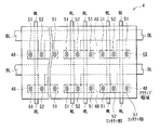
まず、選択トランジスタ等のCMOS回路が形成された基板41(後述の図3)上に、例えば窒化チタンよりなる下部電極10のプラグを形成する。その後、必要であれば逆スパッタ等で、下部電極10の表面上の酸化物等を除去する。
次いで、この下部電極11の表面を室温で酸素雰囲気中にさらす。これにより、下部電極11の表面に酸フッ化膜またはリン酸化膜が形成される。下部電極11の酸化は、酸素雰囲気へのサンプルの投入の他、例えばプラズマ酸化等の積極的な酸化処理を行うようにしてもよい。また、別工程により酸フッ化膜またはリン酸化膜を、下部電極11上に形成してもよい。
Priority Applications (5)
| Application Number | Priority Date | Filing Date | Title |
|---|---|---|---|
| JP2011124610A JP5708929B2 (ja) | 2010-12-13 | 2011-06-02 | 記憶素子およびその製造方法、並びに記憶装置 |
| KR1020110114291A KR101984308B1 (ko) | 2010-12-13 | 2011-11-04 | 기억 소자 및 그 제조 방법, 및 기억 장치 |
| TW100142578A TWI462356B (zh) | 2010-12-13 | 2011-11-21 | 記憶體元件及其製造方法及記憶體裝置 |
| US13/310,830 US9112149B2 (en) | 2010-12-13 | 2011-12-05 | Memory element and method of manufacturing the same, and memory device |
| CN201110399205.8A CN102569335B (zh) | 2010-12-13 | 2011-12-05 | 存储元件、存储元件制造方法和存储装置 |
Applications Claiming Priority (3)
| Application Number | Priority Date | Filing Date | Title |
|---|---|---|---|
| JP2010276749 | 2010-12-13 | ||
| JP2010276749 | 2010-12-13 | ||
| JP2011124610A JP5708929B2 (ja) | 2010-12-13 | 2011-06-02 | 記憶素子およびその製造方法、並びに記憶装置 |
Publications (3)
| Publication Number | Publication Date |
|---|---|
| JP2012142543A JP2012142543A (ja) | 2012-07-26 |
| JP2012142543A5 true JP2012142543A5 (ja) | 2014-06-26 |
| JP5708929B2 JP5708929B2 (ja) | 2015-04-30 |
Family
ID=46198412
Family Applications (1)
| Application Number | Title | Priority Date | Filing Date |
|---|---|---|---|
| JP2011124610A Expired - Fee Related JP5708929B2 (ja) | 2010-12-13 | 2011-06-02 | 記憶素子およびその製造方法、並びに記憶装置 |
Country Status (5)
| Country | Link |
|---|---|
| US (1) | US9112149B2 (ja) |
| JP (1) | JP5708929B2 (ja) |
| KR (1) | KR101984308B1 (ja) |
| CN (1) | CN102569335B (ja) |
| TW (1) | TWI462356B (ja) |
Families Citing this family (11)
| Publication number | Priority date | Publication date | Assignee | Title |
|---|---|---|---|---|
| US9472756B2 (en) * | 2012-09-07 | 2016-10-18 | Kabushiki Kaisha Toshiba | Nonvolatile memory device |
| JP6251688B2 (ja) * | 2012-12-26 | 2017-12-20 | ソニーセミコンダクタソリューションズ株式会社 | 記憶装置およびその製造方法 |
| US20140264224A1 (en) * | 2013-03-14 | 2014-09-18 | Intermolecular, Inc. | Performance Enhancement of Forming-Free ReRAM Devices Using 3D Nanoparticles |
| US8981334B1 (en) * | 2013-11-01 | 2015-03-17 | Micron Technology, Inc. | Memory cells having regions containing one or both of carbon and boron |
| KR20160131097A (ko) * | 2014-03-28 | 2016-11-15 | 제이엑스금속주식회사 | Al-Te-Cu-Zr 합금으로 이루어지는 스퍼터링 타깃 및 그 제조 방법 |
| WO2016056612A1 (ja) * | 2014-10-09 | 2016-04-14 | Jx金属株式会社 | Al-Te-Cu-Zr系合金からなるスパッタリングターゲット及びその製造方法 |
| CN106601909B (zh) * | 2016-12-20 | 2019-08-02 | 南京邮电大学 | 一种卟啉忆阻器及其制备方法 |
| CN107732010B (zh) * | 2017-09-29 | 2020-07-10 | 华中科技大学 | 一种选通管器件及其制备方法 |
| KR20190067668A (ko) * | 2017-12-07 | 2019-06-17 | 에스케이하이닉스 주식회사 | 저항 변화 소자 |
| WO2020138975A1 (ko) * | 2018-12-26 | 2020-07-02 | 한양대학교 에리카산학협력단 | 메모리 소자 및 그 제조 방법 |
| JP2021048258A (ja) * | 2019-09-18 | 2021-03-25 | キオクシア株式会社 | 抵抗変化素子 |
Family Cites Families (18)
| Publication number | Priority date | Publication date | Assignee | Title |
|---|---|---|---|---|
| JP4792714B2 (ja) * | 2003-11-28 | 2011-10-12 | ソニー株式会社 | 記憶素子及び記憶装置 |
| US7199394B2 (en) * | 2004-08-17 | 2007-04-03 | Spansion Llc | Polymer memory device with variable period of retention time |
| US20060245235A1 (en) * | 2005-05-02 | 2006-11-02 | Advanced Micro Devices, Inc. | Design and operation of a resistance switching memory cell with diode |
| JP3913258B2 (ja) * | 2005-06-30 | 2007-05-09 | シャープ株式会社 | 半導体記憶装置 |
| JP2008135659A (ja) * | 2006-11-29 | 2008-06-12 | Sony Corp | 記憶素子、記憶装置 |
| US8097878B2 (en) * | 2007-03-05 | 2012-01-17 | Intermolecular, Inc. | Nonvolatile memory elements with metal-deficient resistive-switching metal oxides |
| JP2008251108A (ja) * | 2007-03-30 | 2008-10-16 | Toshiba Corp | 情報記録再生装置 |
| JP2009043905A (ja) * | 2007-08-08 | 2009-02-26 | Hitachi Ltd | 半導体装置 |
| JP5050813B2 (ja) * | 2007-11-29 | 2012-10-17 | ソニー株式会社 | メモリセル |
| JP5257573B2 (ja) * | 2007-12-06 | 2013-08-07 | ソニー株式会社 | 記憶素子および記憶装置 |
| JP4466738B2 (ja) * | 2008-01-09 | 2010-05-26 | ソニー株式会社 | 記憶素子および記憶装置 |
| WO2009122583A1 (ja) * | 2008-04-03 | 2009-10-08 | 株式会社 東芝 | 不揮発性記憶装置及びその製造方法 |
| WO2009154266A1 (ja) * | 2008-06-20 | 2009-12-23 | 日本電気株式会社 | 半導体記憶装置及びその動作方法 |
| TWI426551B (zh) * | 2009-03-25 | 2014-02-11 | Ind Tech Res Inst | 立體金屬氧化物電極及其製造方法 |
| JP2010278275A (ja) * | 2009-05-29 | 2010-12-09 | Sony Corp | 半導体記憶装置 |
| JP2011124511A (ja) * | 2009-12-14 | 2011-06-23 | Sony Corp | 記憶素子および記憶装置 |
| US8487292B2 (en) * | 2010-03-16 | 2013-07-16 | Sandisk 3D Llc | Resistance-switching memory cell with heavily doped metal oxide layer |
| US8427859B2 (en) * | 2010-04-22 | 2013-04-23 | Micron Technology, Inc. | Arrays of vertically stacked tiers of non-volatile cross point memory cells, methods of forming arrays of vertically stacked tiers of non-volatile cross point memory cells, and methods of reading a data value stored by an array of vertically stacked tiers of non-volatile cross point memory cells |
-
2011
- 2011-06-02 JP JP2011124610A patent/JP5708929B2/ja not_active Expired - Fee Related
- 2011-11-04 KR KR1020110114291A patent/KR101984308B1/ko active IP Right Grant
- 2011-11-21 TW TW100142578A patent/TWI462356B/zh not_active IP Right Cessation
- 2011-12-05 US US13/310,830 patent/US9112149B2/en not_active Expired - Fee Related
- 2011-12-05 CN CN201110399205.8A patent/CN102569335B/zh not_active Expired - Fee Related
Similar Documents
| Publication | Publication Date | Title |
|---|---|---|
| JP2012142543A5 (ja) | ||
| JP2012009837A5 (ja) | 半導体装置の作製方法 | |
| JP2013084939A5 (ja) | 半導体装置の作製方法 | |
| JP2013102154A5 (ja) | 半導体装置の作製方法 | |
| JP2014179625A5 (ja) | ||
| JP2010034523A5 (ja) | ||
| JP2012146946A5 (ja) | ||
| JP2010080947A5 (ja) | 半導体装置の作製方法 | |
| JP2011029637A5 (ja) | ||
| JP2012009838A5 (ja) | 半導体装置の作製方法 | |
| JP2011205089A5 (ja) | 半導体膜の作製方法 | |
| JP2012102113A5 (ja) | ||
| JP2013110397A5 (ja) | ||
| WO2012154429A3 (en) | Methods of dry stripping boron-carbon films | |
| JP2010103360A5 (ja) | 半導体装置の作製方法、酸化物半導体、薄膜トランジスタ及び表示装置 | |
| JP2012004549A5 (ja) | 半導体装置 | |
| JP2011258939A5 (ja) | ||
| WO2013177269A3 (en) | Zirconium-containing precursors for vapor deposition | |
| JP2015073092A5 (ja) | 半導体装置の作製方法 | |
| JP2010135762A5 (ja) | 半導体装置の作製方法 | |
| JP2014199905A5 (ja) | 半導体装置の作製方法 | |
| JP2016528378A5 (ja) | ||
| JP2012033911A5 (ja) | ||
| JP2014007393A5 (ja) | 半導体装置の作製方法 | |
| JP2011091388A5 (ja) | 半導体装置の作製方法 |