JP2010141685A - パルス遅延回路およびa/d変換回路 - Google Patents
パルス遅延回路およびa/d変換回路 Download PDFInfo
- Publication number
- JP2010141685A JP2010141685A JP2008316969A JP2008316969A JP2010141685A JP 2010141685 A JP2010141685 A JP 2010141685A JP 2008316969 A JP2008316969 A JP 2008316969A JP 2008316969 A JP2008316969 A JP 2008316969A JP 2010141685 A JP2010141685 A JP 2010141685A
- Authority
- JP
- Japan
- Prior art keywords
- circuit
- delay
- pulse
- signal
- delay unit
- Prior art date
- Legal status (The legal status is an assumption and is not a legal conclusion. Google has not performed a legal analysis and makes no representation as to the accuracy of the status listed.)
- Granted
Links
Images
Classifications
-
- H—ELECTRICITY
- H03—ELECTRONIC CIRCUITRY
- H03M—CODING; DECODING; CODE CONVERSION IN GENERAL
- H03M1/00—Analogue/digital conversion; Digital/analogue conversion
- H03M1/06—Continuously compensating for, or preventing, undesired influence of physical parameters
- H03M1/08—Continuously compensating for, or preventing, undesired influence of physical parameters of noise
- H03M1/0845—Continuously compensating for, or preventing, undesired influence of physical parameters of noise of power supply variations, e.g. ripple
-
- H—ELECTRICITY
- H03—ELECTRONIC CIRCUITRY
- H03M—CODING; DECODING; CODE CONVERSION IN GENERAL
- H03M1/00—Analogue/digital conversion; Digital/analogue conversion
- H03M1/12—Analogue/digital converters
- H03M1/14—Conversion in steps with each step involving the same or a different conversion means and delivering more than one bit
- H03M1/145—Conversion in steps with each step involving the same or a different conversion means and delivering more than one bit the steps being performed sequentially in series-connected stages
-
- H—ELECTRICITY
- H03—ELECTRONIC CIRCUITRY
- H03M—CODING; DECODING; CODE CONVERSION IN GENERAL
- H03M1/00—Analogue/digital conversion; Digital/analogue conversion
- H03M1/12—Analogue/digital converters
- H03M1/50—Analogue/digital converters with intermediate conversion to time interval
- H03M1/502—Analogue/digital converters with intermediate conversion to time interval using tapped delay lines
-
- H—ELECTRICITY
- H03—ELECTRONIC CIRCUITRY
- H03M—CODING; DECODING; CODE CONVERSION IN GENERAL
- H03M1/00—Analogue/digital conversion; Digital/analogue conversion
- H03M1/12—Analogue/digital converters
- H03M1/60—Analogue/digital converters with intermediate conversion to frequency of pulses
Landscapes
- Engineering & Computer Science (AREA)
- Theoretical Computer Science (AREA)
- Analogue/Digital Conversion (AREA)
- Pulse Circuits (AREA)
Abstract
【解決手段】パルス信号PAを遅延させて出力する遅延ユニットDUをM(Mは正整数)段直列接続してなるパルス遅延回路10と、サンプリングクロックCKSのタイミングで、パルス遅延回路10内でのパルス信号PAの到達位置を検出(ラッチ)し、その検出結果を、パルス信号PAが通過した遅延ユニットDUの段数を表す所定ビットのデジタルデータDTに変換して出力するラッチ&エンコーダ11とを備えたA/D変換回路1において、各遅延ユニットDUには、バッファ12を介して、A/D変換対象となる入力信号Vinを駆動電圧として印加すると共に、バッファ12の出力を各遅延ユニットDUに供給する信号ラインとグランドラインとの間にコンデンサ13を設ける。
【選択図】図1
Description
[第1実施形態]
<全体構成>
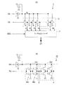
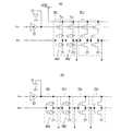
図1(a)は、本発明が適用されたA/D変換回路1の全体構成図である。
このように構成されたA/D変換回路1では、初段の遅延ユニットDUにパルス信号PAを供給すると共に、このパルス信号PAの入力後、サンプリング周期TSが経過した時点で立ち上がるサンプリングクロックCKSを供給すると、ラッチ&エンコーダ11からは、入力信号Vinの電圧レベルを表すデジタルデータ(A/D変換データ)DTが出力される。
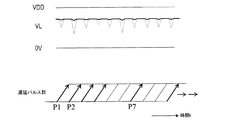
以上説明したように、A/D変換回路1では、遅延ユニットDUのスイッチング動作時に、瞬時的な動作電流が流れても、コンデンサ13が必要な電流を供給することによって、バッファ12の出力抵抗Rやバッファ12の入力側の配線抵抗には、殆ど電流がながれないため、遅延ユニットDUに供給される電圧レベルVLの降下が大幅に軽減される。
[第2実施形態]
次に、第2実施形態について説明する。
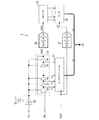
図3に示すように、A/D変換回路3は、パルス信号PAを所定の遅延時間だけ遅延させて出力するM(=2a :aは正整数)個の遅延ユニットDUをリング状に連結することにより、パルス信号PAを周回させることができるリングディレイライン(RDL)として構成されたパルス遅延回路30と、サンプリングクロックCKSの立ち上がりタイミングで、パルス遅延回路30内でのパルス信号PAの到達位置を検出(ラッチ)し、その検出結果を、パルス信号PAが通過した遅延ユニットDUが先頭から何段目にあるかを表すaビットのデジタルデータ(A/D変換データ)に変換して出力するラッチ&エンコーダ31とを備えている。
このように構成されたA/D変換回路3では、ラッチ&エンコーダ31は、第1実施形態におけるラッチ&エンコーダ11と同様に動作する。周回数カウンタ36は、動作クロックCKAに従って、パルス遅延回路30内でのパルス信号PAの周回回数をカウントし、ラッチ回路38は、ラッチパルスLPに従って、周回数カウンタ36のカウント値をラッチする。
このように構成されたA/D変換回路3では、バッファ32の出力を各遅延ユニットDUに供給する信号ラインとグランドラインとの間にコンデンサ33が設けられているため、第1実施形態のA/D変換回路1と同様の効果を得ることができる。
[第3実施形態]
次に、第3実施形態について説明する。
[他の実施形態]
以上、本発明のいくつかの実施形態について説明したが、本発明は上記実施形態に限定されるものではなく、本発明の要旨を逸脱しない範囲において、様々な態様にて実施することが可能である。
Claims (10)
- 入力信号の電圧レベルに応じた遅延時間でパルス信号を遅延させる複数の遅延ユニットを直列又はリング状に接続してなり、パルス信号を各遅延ユニットの遅延時間にて順次遅延させながら伝送するパルス遅延回路において、
前記入力信号を前記遅延ユニットに供給する信号ラインに、前記遅延ユニットの反転動作時に消費される電力の供給源となる容量素子を設けたことを特徴とするパルス遅延回路。 - 前記信号ラインは、抵抗分を有するバッファ回路を介して前記入力信号の入力端子に接続されていることを特徴とする請求項1に記載のパルス遅延回路。
- 前記容量素子が有する容量分は、該容量分と前記バッファ回路が有する抵抗分とから算出される時定数が前記入力信号について予め規定された最大周波数の逆数より小さな値となるように設定されていることを特徴とする請求項2に記載のパルス遅延回路。
- 前記容量素子は、CMOSプロセスによって形成されたものであることを特徴とする請求項1乃至請求項3のいずれかに記載のパルス遅延回路。
- 前記遅延ユニットは、前記入力信号を駆動電圧として動作するCMOSインバータゲート回路からなることを特徴とする請求項1乃至請求項4のいずれかに記載のパルス遅延回路。
- 前記遅延ユニットは、電源ラインとの間に電流制御用のトランジスタが付加されたCMOSインバータゲート回路からなり、前記入力信号は前記電流制御用のトランジスタの駆動電圧として印加されることを特徴とする請求項1乃至請求項4のいずれかに記載のパルス遅延回路。
- 前記遅延ユニットは、標準セルを用いて構成されていることを特徴とする請求項1乃至請求項4のいずれかに記載のパルス遅延回路。
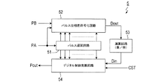
- 請求項1乃至請求項8のいずれかに記載のパルス遅延回路と、
予め設定された測定時間の間に前記パルス遅延回路内で前記パルス信号が通過した前記遅延ユニットの段数に対応する数値データを生成する符号化回路と、
を備え、前記符号化回路が生成する前記数値データを前記入力信号の電圧レベルを表すA/D変換データとして出力することを特徴とするA/D変換回路。 - 前記パルス遅延回路は、前記符号化回路を構成するトランジスタよりサイズの大きいトランジスタを用いて構成されていることを特徴とする請求項8に記載のA/D変換回路。
- 前記パルス遅延回路は、前記遅延ユニットをリング状に接続してなるリングディレイラインからなり、
前記符号化回路は、
前記パルス遅延回路を前記パルス信号が周回した回数をカウントする周回数カウンタと、
前記パルス遅延回路内での前記パルス信号の位置を符号化した値を前記数値データの下位ビットとして出力する下位符号化回路と、
前記周回数カウンタのカウント値を前記数値データの上位ビットとして出力する上位符号化回路と、
を備えることを特徴とする請求項8又は請求項9に記載のA/D変換回路。
Priority Applications (3)
| Application Number | Priority Date | Filing Date | Title |
|---|---|---|---|
| JP2008316969A JP4645734B2 (ja) | 2008-12-12 | 2008-12-12 | パルス遅延回路およびa/d変換回路 |
| DE102009047452.8A DE102009047452B4 (de) | 2008-12-12 | 2009-12-03 | Impulsverzögerungsschaltung und die Impulsverzögerungsschaltung aufweisender A/D-Wandler |
| US12/653,186 US7932848B2 (en) | 2008-12-12 | 2009-12-09 | Pulse delay circuit and A/D converter including same |
Applications Claiming Priority (1)
| Application Number | Priority Date | Filing Date | Title |
|---|---|---|---|
| JP2008316969A JP4645734B2 (ja) | 2008-12-12 | 2008-12-12 | パルス遅延回路およびa/d変換回路 |
Publications (2)
| Publication Number | Publication Date |
|---|---|
| JP2010141685A true JP2010141685A (ja) | 2010-06-24 |
| JP4645734B2 JP4645734B2 (ja) | 2011-03-09 |
Family
ID=42168877
Family Applications (1)
| Application Number | Title | Priority Date | Filing Date |
|---|---|---|---|
| JP2008316969A Active JP4645734B2 (ja) | 2008-12-12 | 2008-12-12 | パルス遅延回路およびa/d変換回路 |
Country Status (3)
| Country | Link |
|---|---|
| US (1) | US7932848B2 (ja) |
| JP (1) | JP4645734B2 (ja) |
| DE (1) | DE102009047452B4 (ja) |
Cited By (2)
| Publication number | Priority date | Publication date | Assignee | Title |
|---|---|---|---|---|
| WO2012002492A1 (ja) * | 2010-07-02 | 2012-01-05 | オリンパス株式会社 | 信号転送回路および撮像装置 |
| US8779343B2 (en) | 2011-01-11 | 2014-07-15 | Olympus Corporation | Solid state image pickup device having an analog signal processing unit including first and second capacitors, a delay circuit and an A/D converting circuit for an image capturing signal process |
Families Citing this family (3)
| Publication number | Priority date | Publication date | Assignee | Title |
|---|---|---|---|---|
| KR101123353B1 (ko) | 2011-09-21 | 2012-03-13 | 홍익대학교 산학협력단 | 피드백 지연 소자를 이용한 지연 고정 루프 회로 |
| US8766682B2 (en) * | 2012-01-24 | 2014-07-01 | Voxtel, Inc. | Method and device for measuring duration of a time interval |
| US11526153B2 (en) * | 2020-11-09 | 2022-12-13 | Analog Devices, Inc. | Programmable delay line with glitch suppression |
Citations (5)
| Publication number | Priority date | Publication date | Assignee | Title |
|---|---|---|---|---|
| JP2003032113A (ja) * | 2001-07-13 | 2003-01-31 | Denso Corp | A/d変換方法及び装置 |
| JP2003046390A (ja) * | 2001-07-31 | 2003-02-14 | Denso Corp | フィルタリング方法及びフィルタ機能を有するa/d変換装置 |
| JP2005322327A (ja) * | 2004-05-10 | 2005-11-17 | Denso Corp | サンプルホールド回路 |
| JP2007134786A (ja) * | 2005-11-08 | 2007-05-31 | Denso Corp | A/d変換回路 |
| JP2007312288A (ja) * | 2006-05-22 | 2007-11-29 | Denso Corp | A/d変換回路 |
Family Cites Families (10)
| Publication number | Priority date | Publication date | Assignee | Title |
|---|---|---|---|---|
| JP3064644B2 (ja) | 1992-03-16 | 2000-07-12 | 株式会社デンソー | A/d変換回路 |
| JP3455982B2 (ja) | 1993-01-14 | 2003-10-14 | 株式会社デンソー | 偶数段リングオシレータ及びパルス位相差符号化回路 |
| JP2900772B2 (ja) | 1993-12-24 | 1999-06-02 | 株式会社デンソー | パルス位相差符号化回路とパルス発生回路との複合装置及びデジタル制御pll装置 |
| US6928128B1 (en) * | 1999-05-03 | 2005-08-09 | Rambus Inc. | Clock alignment circuit having a self regulating voltage supply |
| JP3956847B2 (ja) | 2002-04-24 | 2007-08-08 | 株式会社デンソー | A/d変換方法及び装置 |
| JP3960267B2 (ja) | 2003-05-29 | 2007-08-15 | 株式会社デンソー | A/d変換方法及び装置 |
| JP2007006369A (ja) | 2005-06-27 | 2007-01-11 | Pioneer Electronic Corp | リモコン及びそのリモコンを有する視聴システム |
| JP2007006368A (ja) | 2005-06-27 | 2007-01-11 | Denso Corp | A/d変換回路 |
| TWI312238B (en) * | 2006-04-24 | 2009-07-11 | Ind Tech Res Inst | Delay line and analog-to-digital converting apparatus and load-sensing circuit using the same |
| JP4965203B2 (ja) * | 2006-09-11 | 2012-07-04 | 株式会社リコー | 遅延時間生成回路、それを用いた二次電池保護用半導体装置、バッテリパックおよび電子機器 |
-
2008
- 2008-12-12 JP JP2008316969A patent/JP4645734B2/ja active Active
-
2009
- 2009-12-03 DE DE102009047452.8A patent/DE102009047452B4/de active Active
- 2009-12-09 US US12/653,186 patent/US7932848B2/en active Active
Patent Citations (5)
| Publication number | Priority date | Publication date | Assignee | Title |
|---|---|---|---|---|
| JP2003032113A (ja) * | 2001-07-13 | 2003-01-31 | Denso Corp | A/d変換方法及び装置 |
| JP2003046390A (ja) * | 2001-07-31 | 2003-02-14 | Denso Corp | フィルタリング方法及びフィルタ機能を有するa/d変換装置 |
| JP2005322327A (ja) * | 2004-05-10 | 2005-11-17 | Denso Corp | サンプルホールド回路 |
| JP2007134786A (ja) * | 2005-11-08 | 2007-05-31 | Denso Corp | A/d変換回路 |
| JP2007312288A (ja) * | 2006-05-22 | 2007-11-29 | Denso Corp | A/d変換回路 |
Cited By (4)
| Publication number | Priority date | Publication date | Assignee | Title |
|---|---|---|---|---|
| WO2012002492A1 (ja) * | 2010-07-02 | 2012-01-05 | オリンパス株式会社 | 信号転送回路および撮像装置 |
| JP2012034348A (ja) * | 2010-07-02 | 2012-02-16 | Olympus Corp | 信号転送回路および撮像装置 |
| US8520796B2 (en) | 2010-07-02 | 2013-08-27 | Olympus Corporation | Signal transfer circuit and image pickup device |
| US8779343B2 (en) | 2011-01-11 | 2014-07-15 | Olympus Corporation | Solid state image pickup device having an analog signal processing unit including first and second capacitors, a delay circuit and an A/D converting circuit for an image capturing signal process |
Also Published As
| Publication number | Publication date |
|---|---|
| DE102009047452A1 (de) | 2010-06-17 |
| US20100149016A1 (en) | 2010-06-17 |
| US7932848B2 (en) | 2011-04-26 |
| JP4645734B2 (ja) | 2011-03-09 |
| DE102009047452B4 (de) | 2025-11-06 |
Similar Documents
| Publication | Publication Date | Title |
|---|---|---|
| JP4396063B2 (ja) | A/d変換方法及び装置 | |
| JP4725418B2 (ja) | 時間計測回路 | |
| JP4645734B2 (ja) | パルス遅延回路およびa/d変換回路 | |
| US9128146B2 (en) | Semiconductor integrated circuit | |
| JP3991969B2 (ja) | A/d変換回路 | |
| JP2011223553A (ja) | 増幅回路及びその増幅回路を含むアナログデジタル変換回路 | |
| JP4702179B2 (ja) | A/d変換回路 | |
| EP1995874A1 (en) | A/D converter circuit and A/D conversion method | |
| US9577661B2 (en) | Voltage-controlled oscillator and analog-digital converter | |
| US7248197B2 (en) | A/D converter that is implemented using only digital circuit components and digital signal processing | |
| JP6772998B2 (ja) | A/d変換回路 | |
| JP4921329B2 (ja) | A/d変換回路 | |
| US7653170B2 (en) | Electrical circuit for measuring times and method for measuring times | |
| JP2010246192A (ja) | 電源装置、電源装置の制御回路、電源装置の制御方法 | |
| CN102017424B (zh) | A/d转换电路 | |
| WO2008023624A1 (fr) | Circuit à retard variable, générateur de synchronisation, et appareil pour tester des semi-conducteurs | |
| JP4349266B2 (ja) | A/d変換装置 | |
| JP2007336119A (ja) | 半導体装置、及びインピーダンス制御方法 | |
| JP5282475B2 (ja) | フィルタ回路のトリミング方法 | |
| JP2010283054A (ja) | プロセスモニタ回路およびプロセス特性の判定方法 | |
| JP5564869B2 (ja) | 半導体集積回路 | |
| JP2715979B2 (ja) | 出力バッファ回路 | |
| Ali et al. | Design of configurable digital spike filtering circuits in 130 nm CMOS process | |
| JPH09153802A (ja) | 半導体集積回路 | |
| JP4614785B2 (ja) | 遅延時間評価回路および方法 |
Legal Events
| Date | Code | Title | Description |
|---|---|---|---|
| A621 | Written request for application examination |
Free format text: JAPANESE INTERMEDIATE CODE: A621 Effective date: 20100531 |
|
| A977 | Report on retrieval |
Free format text: JAPANESE INTERMEDIATE CODE: A971007 Effective date: 20100820 |
|
| A131 | Notification of reasons for refusal |
Free format text: JAPANESE INTERMEDIATE CODE: A131 Effective date: 20100824 |
|
| A521 | Request for written amendment filed |
Free format text: JAPANESE INTERMEDIATE CODE: A523 Effective date: 20101020 |
|
| TRDD | Decision of grant or rejection written | ||
| A01 | Written decision to grant a patent or to grant a registration (utility model) |
Free format text: JAPANESE INTERMEDIATE CODE: A01 Effective date: 20101109 |
|
| A01 | Written decision to grant a patent or to grant a registration (utility model) |
Free format text: JAPANESE INTERMEDIATE CODE: A01 |
|
| A61 | First payment of annual fees (during grant procedure) |
Free format text: JAPANESE INTERMEDIATE CODE: A61 Effective date: 20101122 |
|
| FPAY | Renewal fee payment (event date is renewal date of database) |
Free format text: PAYMENT UNTIL: 20131217 Year of fee payment: 3 |
|
| R151 | Written notification of patent or utility model registration |
Ref document number: 4645734 Country of ref document: JP Free format text: JAPANESE INTERMEDIATE CODE: R151 |
|
| FPAY | Renewal fee payment (event date is renewal date of database) |
Free format text: PAYMENT UNTIL: 20131217 Year of fee payment: 3 |
|
| R250 | Receipt of annual fees |
Free format text: JAPANESE INTERMEDIATE CODE: R250 |
|
| R250 | Receipt of annual fees |
Free format text: JAPANESE INTERMEDIATE CODE: R250 |
|
| R250 | Receipt of annual fees |
Free format text: JAPANESE INTERMEDIATE CODE: R250 |
|
| R250 | Receipt of annual fees |
Free format text: JAPANESE INTERMEDIATE CODE: R250 |
|
| R250 | Receipt of annual fees |
Free format text: JAPANESE INTERMEDIATE CODE: R250 |
|
| R250 | Receipt of annual fees |
Free format text: JAPANESE INTERMEDIATE CODE: R250 |
|
| R250 | Receipt of annual fees |
Free format text: JAPANESE INTERMEDIATE CODE: R250 |
|
| R250 | Receipt of annual fees |
Free format text: JAPANESE INTERMEDIATE CODE: R250 |
|
| R250 | Receipt of annual fees |
Free format text: JAPANESE INTERMEDIATE CODE: R250 |
|
| R250 | Receipt of annual fees |
Free format text: JAPANESE INTERMEDIATE CODE: R250 |
|
| R250 | Receipt of annual fees |
Free format text: JAPANESE INTERMEDIATE CODE: R250 |