JP2010141685A - Pulse delay circuit and A / D conversion circuit - Google Patents
Pulse delay circuit and A / D conversion circuit Download PDFInfo
- Publication number
- JP2010141685A JP2010141685A JP2008316969A JP2008316969A JP2010141685A JP 2010141685 A JP2010141685 A JP 2010141685A JP 2008316969 A JP2008316969 A JP 2008316969A JP 2008316969 A JP2008316969 A JP 2008316969A JP 2010141685 A JP2010141685 A JP 2010141685A
- Authority
- JP
- Japan
- Prior art keywords
- circuit
- delay
- pulse
- signal
- delay unit
- Prior art date
- Legal status (The legal status is an assumption and is not a legal conclusion. Google has not performed a legal analysis and makes no representation as to the accuracy of the status listed.)
- Granted
Links
Images
Classifications
-
- H—ELECTRICITY
- H03—ELECTRONIC CIRCUITRY
- H03M—CODING; DECODING; CODE CONVERSION IN GENERAL
- H03M1/00—Analogue/digital conversion; Digital/analogue conversion
- H03M1/06—Continuously compensating for, or preventing, undesired influence of physical parameters
- H03M1/08—Continuously compensating for, or preventing, undesired influence of physical parameters of noise
- H03M1/0845—Continuously compensating for, or preventing, undesired influence of physical parameters of noise of power supply variations, e.g. ripple
-
- H—ELECTRICITY
- H03—ELECTRONIC CIRCUITRY
- H03M—CODING; DECODING; CODE CONVERSION IN GENERAL
- H03M1/00—Analogue/digital conversion; Digital/analogue conversion
- H03M1/12—Analogue/digital converters
- H03M1/14—Conversion in steps with each step involving the same or a different conversion means and delivering more than one bit
- H03M1/145—Conversion in steps with each step involving the same or a different conversion means and delivering more than one bit the steps being performed sequentially in series-connected stages
-
- H—ELECTRICITY
- H03—ELECTRONIC CIRCUITRY
- H03M—CODING; DECODING; CODE CONVERSION IN GENERAL
- H03M1/00—Analogue/digital conversion; Digital/analogue conversion
- H03M1/12—Analogue/digital converters
- H03M1/50—Analogue/digital converters with intermediate conversion to time interval
- H03M1/502—Analogue/digital converters with intermediate conversion to time interval using tapped delay lines
-
- H—ELECTRICITY
- H03—ELECTRONIC CIRCUITRY
- H03M—CODING; DECODING; CODE CONVERSION IN GENERAL
- H03M1/00—Analogue/digital conversion; Digital/analogue conversion
- H03M1/12—Analogue/digital converters
- H03M1/60—Analogue/digital converters with intermediate conversion to frequency of pulses
Landscapes
- Engineering & Computer Science (AREA)
- Theoretical Computer Science (AREA)
- Analogue/Digital Conversion (AREA)
- Pulse Circuits (AREA)
Abstract
Description
本発明は、入力信号の電圧レベルに応じた遅延時間でパルス信号を遅延させる複数の遅延ユニットで構成されたパルス遅延回路、及びそのパルス遅延回路を用いて構成されたA/D変換回路に関する。 The present invention relates to a pulse delay circuit configured by a plurality of delay units that delay a pulse signal by a delay time corresponding to a voltage level of an input signal, and an A / D conversion circuit configured using the pulse delay circuit.
従来より、全ての部分がデジタル回路により構成されたパルス遅延型(TAD方式)のAD変換回路が知られている。 2. Description of the Related Art Conventionally, a pulse delay type (TAD method) AD converter circuit in which all parts are constituted by digital circuits is known.
このTAD方式のA/D変換回路は、入力信号の電圧レベルに応じた遅延時間でパルス信号を遅延させて出力する遅延ユニットを複数段直列又はリング状に接続してなるパルス遅延回路を用いて構成され、予め設定された測定時間の間に、パルス遅延回路内でパルス信号が通過した遅延ユニットの段数に対応する数値データを、A/D変換データとして出力する。また、TAD方式のA/D変換回路は、デジタル回路のみで構成されているため、CMOSデジタル回路IC製造技術だけを用いて安価かつ容易に製造することができる。 This TAD type A / D conversion circuit uses a pulse delay circuit in which a delay unit that delays and outputs a pulse signal by a delay time corresponding to the voltage level of an input signal is connected in a plurality of stages in series or in a ring shape. The numerical data corresponding to the number of stages of the delay unit through which the pulse signal has passed in the pulse delay circuit during the preset measurement time is output as A / D conversion data. Further, since the TAD type A / D conversion circuit is composed of only a digital circuit, it can be manufactured inexpensively and easily using only the CMOS digital circuit IC manufacturing technology.
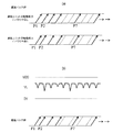
ところで、TAD方式のA/D変換回路を安定に動作させるには、パルス遅延回路を構成する全ての遅延ユニットでの遅延を均一にして、パルスを均等な速度で遅延伝播させる必要がある(図6(a)上段参照)。なお、図6は、パルス遅延回路にパルス信号を入力した場合における各遅延ユニットの出力の変化を模式的に示した説明図であり、図中のPiはi段目の遅延ユニットの出力であることを示す。 By the way, in order to stably operate the TAD type A / D conversion circuit, it is necessary to make the delays in all the delay units constituting the pulse delay circuit uniform and to propagate the pulses at an equal speed (see FIG. 6 (a) Refer to the upper stage). FIG. 6 is an explanatory diagram schematically showing changes in the output of each delay unit when a pulse signal is input to the pulse delay circuit, and Pi in the figure is the output of the i-th delay unit. It shows that.
しかし、CMOSデジタル回路の微細化に伴い、トランジスタ加工時における加工誤差や微細ゴミの影響は相対的に大きくなっている。これらの影響で、遅延ユニットを構成する各トランジスタの駆動能力がばらつくと、図6(b)に示すように、各遅延ユニットの遅延時間にばらつきが生じ、A/D変換データの分解能(1LSBに対応する入力電圧幅)のバラツキが大きくなってしまう。 However, with the miniaturization of CMOS digital circuits, the effects of processing errors and fine dust during transistor processing are relatively large. Due to these effects, if the drive capability of each of the transistors constituting the delay unit varies, the delay time of each delay unit varies as shown in FIG. 6B, and the resolution of the A / D conversion data (1LSB is reduced). The variation of the corresponding input voltage width becomes large.
これに対して、A/D変換データの精度に影響を与えるパルス遅延回路を構成するトランジスタのサイズを、パルス遅延回路以外の部分と比較して大きくすることで、加工誤差や微細ゴミ等の影響を相対的に軽減することも行われている(例えば、特許文献1参照)。
また、パルス遅延回路を構成する遅延ユニットは、通常、CMOSインバータゲート回路を用いて構成されているため、遅延ユニットの出力信号が反転する毎に、遅延ユニットに貫通電流が流れ、遅延ユニットの電源ライン、即ち、入力信号が印加される信号ラインに、スイッチングノイズが重畳されてしまう。 In addition, since the delay unit constituting the pulse delay circuit is usually configured using a CMOS inverter gate circuit, a through current flows through the delay unit every time the output signal of the delay unit is inverted, and the delay unit power supply Switching noise is superimposed on the line, that is, the signal line to which the input signal is applied.
しかも、上述したようにパルス遅延回路を構成するトランジスタのサイズを大きくすると、各遅延ユニットで消費される電力も増大するため、スイッチングノイズが大きくなってしまう。 In addition, as described above, when the size of the transistors constituting the pulse delay circuit is increased, the power consumed by each delay unit also increases, resulting in an increase in switching noise.
その結果、入力信号の信号レベルがスイッチングノイズによって変動することになるため、その変動によって各遅延ユニットでの遅延にバラツキが発生してしまい(図6(b)参照)、パルス遅延回路は、均等な時間間隔の遅延パルスを発生させることができず、ひいては、A/D変換データの精度を劣化させてしまうという問題があった。 As a result, the signal level of the input signal fluctuates due to switching noise, which causes variations in delay in each delay unit (see FIG. 6B), and the pulse delay circuit is uniform. There is a problem that it is impossible to generate a delay pulse with a short time interval, and as a result, the accuracy of the A / D conversion data is deteriorated.
本発明は、上記問題点を解決するために、均等な時間間隔の遅延パルスが得られるパルス遅延回路、及び、A/D変換データの分解能が均一なA/D変換回路を提供することを目的とする。 In order to solve the above problems, an object of the present invention is to provide a pulse delay circuit capable of obtaining delayed pulses at equal time intervals, and an A / D conversion circuit having uniform resolution of A / D conversion data. And
上記目的を達成するためになされた請求項1に記載のパルス遅延回路は、入力信号の電圧レベルに応じた遅延時間でパルス信号を遅延させる複数の遅延ユニットを直列又はリング状に接続してなり、パルス信号を各遅延ユニットの遅延時間にて順次遅延させながら伝送するように構成されている。
In order to achieve the above object, the pulse delay circuit according to
そして、入力信号を遅延ユニットに供給する信号ラインには、遅延ユニットの反転動作時に消費される電力の供給源となる容量素子が設けられている。 The signal line that supplies the input signal to the delay unit is provided with a capacitive element that serves as a supply source of power consumed during the inversion operation of the delay unit.
このように構成された本発明のパルス遅延回路によれば、遅延ユニットが反転動作をする際に、容量素子から電力が供給されるため、信号ライン上でのスイッチングノイズの発生を抑制することができ、その結果、各遅延ユニットから均一な時間間隔の遅延パルスを発生させることができる。 According to the pulse delay circuit of the present invention configured as described above, when the delay unit performs the inverting operation, power is supplied from the capacitive element, so that the occurrence of switching noise on the signal line can be suppressed. As a result, a delay pulse having a uniform time interval can be generated from each delay unit.
ところで、信号ラインは、請求項2に記載のように、抵抗分を有するバッファ回路を介して入力信号の入力端子に接続されていることが望ましい。 By the way, as described in claim 2, the signal line is preferably connected to the input terminal of the input signal through a buffer circuit having a resistance component.
この場合、入力端子からバッファ回路を介して入力信号を取り込むことになるため、入力端子を介して外部より侵入するノイズの影響を軽減することができると共に、遅延ユニットの反転動作により信号ラインに重畳されたスイッチングノイズ(電圧変動)が入力端子を介して外部に与える影響を軽減することができる。 In this case, since the input signal is captured from the input terminal via the buffer circuit, it is possible to reduce the influence of noise entering from the outside via the input terminal and to superimpose it on the signal line by the inversion operation of the delay unit. The effect of the switching noise (voltage fluctuation) applied to the outside via the input terminal can be reduced.
なお、請求項3に記載のように、容量素子が有する容量分は、その容量分とバッファ回路が有する抵抗分とから算出される時定数が入力信号について予め規定された最大周波数の逆数より小さな値となるように設定されていることが望ましい。 According to the third aspect of the present invention, the capacitance of the capacitive element is such that the time constant calculated from the capacitance and the resistance of the buffer circuit is smaller than the reciprocal of the maximum frequency defined in advance for the input signal. It is desirable to set the value.
但し、最大周波数とは、入力信号の信号成分として供給される可能性のある周波数のうち最大のもののことである。従って、本発明のパルス遅延回路によれば、入力信号よりも高い周波数を有する不要ノイズを除去することができる。 However, the maximum frequency is the maximum frequency that can be supplied as a signal component of the input signal. Therefore, according to the pulse delay circuit of the present invention, unnecessary noise having a frequency higher than that of the input signal can be removed.
また、請求項4に記載のように、容量素子は、CMOSプロセスによって形成されたものであることが望ましい。 According to a fourth aspect of the present invention, the capacitive element is preferably formed by a CMOS process.
この場合、容量素子を、同じくCMOSプロセスによって形成可能なパルス遅延経路と同じICチップ上に形成することができる。 In this case, the capacitive element can be formed on the same IC chip as the pulse delay path that can also be formed by the CMOS process.
ところで、遅延ユニットは、請求項5に記載のように、入力信号を駆動電圧として動作するCMOSインバータゲート回路で構成されていてもよいし、請求項6に記載のように、電源ラインとの間に電流制御用のトランジスタが付加されたCMOSインバータゲート回路からなり、入力信号は電流制御用のトランジスタの駆動電圧として印加されるように構成されていてもよい。
By the way, the delay unit may be composed of a CMOS inverter gate circuit that operates using an input signal as a drive voltage, as described in
また、遅延ユニットは、請求項7に記載のように、標準セルを用いて構成されていてもよい。このように標準セルを用いることによって、パルス遅延回路を搭載したICを設計する際の手間を軽減することができる。なお、標準セルとしては、AND,OR,NAND,NOR等の論理回路を用いることができる。 The delay unit may be configured using a standard cell as described in claim 7. By using the standard cell in this way, it is possible to reduce time and labor when designing an IC equipped with a pulse delay circuit. As standard cells, logic circuits such as AND, OR, NAND, and NOR can be used.
次に、請求項8に記載のA/D変換回路は、請求項1乃至請求項8のいずれかに記載のパルス遅延回路と、予め設定された測定時間の間にパルス遅延回路内でパルス信号が通過した遅延ユニットの段数に対応する数値データを生成する符号化回路とを備え、符号化回路が生成する数値データを入力信号の電圧レベルを表すA/D変換データとして出力する。 Next, an A / D conversion circuit according to an eighth aspect includes a pulse delay circuit according to any one of the first to eighth aspects and a pulse signal in the pulse delay circuit between a preset measurement time. And an encoding circuit that generates numerical data corresponding to the number of stages of delay units that have passed through, and outputs the numerical data generated by the encoding circuit as A / D conversion data representing the voltage level of the input signal.
このように構成された本発明のA/D変換回路によれば、パルス遅延回路を構成する各遅延ユニットから均一な時間間隔の遅延パルスが得られるため、1LSBの値が均一な精度の高いA/D変換データを得ることができる。 According to the A / D conversion circuit of the present invention configured as described above, delay pulses having a uniform time interval can be obtained from each delay unit constituting the pulse delay circuit. / D conversion data can be obtained.
なお、請求項9に記載のように、パルス遅延回路は、符号化回路を構成するトランジスタよりサイズの大きいトランジスタを用いて構成されていることが望ましい。 In addition, as described in claim 9, it is desirable that the pulse delay circuit is configured using a transistor having a size larger than that of the transistor configuring the encoding circuit.
この場合、トランジスタ加工時における加工誤差や微細ゴミがA/D変換データに与える影響を抑制することができ、より精度の高い遅延パルスやA/D変換データを得ることができる。 In this case, the influence of processing errors and fine dust on the A / D conversion data during transistor processing can be suppressed, and more accurate delay pulses and A / D conversion data can be obtained.
また、請求項10に記載のように、パルス遅延回路は、遅延ユニットをリング状に接続してなるリングディレイラインからなり、符号化回路が、パルス遅延回路をパルス信号が周回した回数をカウントする周回数カウンタと、パルス遅延回路内でのパルス信号の位置を符号化した値を数値データの下位ビットとして出力する下位符号化回路と、周回数カウンタのカウント値を数値データの上位ビットとして出力する上位符号化回路とで構成されていてもよい。 According to a tenth aspect of the present invention, the pulse delay circuit includes a ring delay line formed by connecting delay units in a ring shape, and the encoding circuit counts the number of times the pulse signal circulates the pulse delay circuit. A lap counter, a lower encoding circuit that outputs a value obtained by encoding the position of the pulse signal in the pulse delay circuit as lower bits of the numerical data, and a count value of the lap counter is output as upper bits of the numerical data. It may be composed of a higher-order encoding circuit.
このようにパルス遅延回路をリング状に構成することによって、容量素子が電力供給をすべき遅延ユニットの数を大幅に削減することが可能となり、容量素子を挿入することによる安定効果(スイッチングノイズの除去能力)を向上させることができる。 By configuring the pulse delay circuit in a ring shape in this way, the number of delay units to be supplied by the capacitive element can be greatly reduced, and the stability effect (switching noise reduction) by inserting the capacitive element can be reduced. (Removal ability) can be improved.
以下に本発明の実施形態を図面と共に説明する。
[第1実施形態]
<全体構成>
図1(a)は、本発明が適用されたA/D変換回路1の全体構成図である。
Embodiments of the present invention will be described below with reference to the drawings.
[First Embodiment]
<Overall configuration>
FIG. 1A is an overall configuration diagram of an A /
A/D変換回路1は、図1(a)に示すように、パルス信号PAを所定の遅延時間だけ遅延させて出力する遅延ユニットDUをM(Mは正整数)段直列接続してなるストレートディレイライン(SDL)として構成されたパルス遅延回路10と、サンプリングクロックCKSの立ち上がりタイミングで、パルス遅延回路10内でのパルス信号PAの到達位置を検出(ラッチ)し、その検出結果を、パルス信号PAが通過した遅延ユニットDUが先頭から何段目にあるかを表す所定ビットのデジタルデータ(A/D変換データ)DTに変換して出力する符号化回路としてのラッチ&エンコーダ11とから構成されている。なお、図中の符号Pi(i=1,2,…M)は、i段目の遅延ユニットDUの出力を示す。
As shown in FIG. 1A, the A /
また、パルス遅延回路10を構成する各遅延ユニットDUは、図1(b)に示すように、CMOSインバータゲート回路INVを2段直列接続してなり、入力信号を遅延させて出力するように構成されている。
In addition, each delay unit DU constituting the
そして、各遅延ユニットDUには、バッファ12を介して、A/D変換対象となる入力信号Vinが駆動電圧として印加されている。従って、各遅延ユニットDUの遅延時間は、入力信号Vinの電圧レベルに対応した時間となり、サンプリングクロックCKSの一周期、即ちサンプリング周期(測定時間)TS内にパルス遅延回路10内でのパルス信号PAが通過する遅延ユニットDUの段数は、入力信号Vinの電圧レベル(測定時間TSの間の平均電圧レベル)に比例したものとなる。
An input signal Vin to be A / D converted is applied as a drive voltage to each delay unit DU via the
また、バッファ12の出力を各遅延ユニットDUに供給する信号ラインとグランドラインとの間には、コンデンサ13が設けられている。但し、バッファ12の出力抵抗をR、コンデンサ13の容量をCとして、これらR,Cから算出される時定数が、入力信号Vinとして許容される信号成分の最大周波数の逆数(最大周波数となる信号成分の1波長分の周期)より小さな値となるように、コンデンサ13の容量Cは設定されている。
A
一方、ラッチ&エンコーダ11は、パルス遅延回路10を構成する各遅延ユニットDUの出力P1〜PMをラッチするラッチ回路、そのラッチ回路の出力をデジタルデータDTに変換するエンコーダを少なくとも備えており、これらはいずれも一定の電源電圧で駆動されるように構成されている。
On the other hand, the latch &
ところで、A/D変換回路1は、コンデンサ13も含めた全ての部位が、CMOS製造プロセスを使用して半導体基板(ICチップ)上の半導体集積回路として構成される。
By the way, in the A /
但し、A/D変換回路1のうち、論理演算回路であるラッチ&エンコーダ11は、当該半導体集積回路に適用するCMOSデジタル回路設計ルールの最小サイズ(例えば最小線幅が90nm)で設計されたトランジスタを用いて構成され、また、各遅延ユニットDUでの遅延を均一にすべきパルス遅延回路10は、ラッチ&エンコーダ11を構成するトランジスタより、大きなサイズに設計されたトランジスタを用いて構成されている。
However, in the A /
また、バッファ12やコンデンサ13は、バッファ12の出力抵抗及びバッファ12の出力から各遅延ユニットDUに至る信号ラインの配線抵抗の合計が、遅延ユニットDUのオン抵抗に対して1/10程度(望ましくは1/100程度)となるように配置されている。具体的には、パルス遅延回路10から1mm(望ましくは100μm)以内に配置される。
In the
<動作>
このように構成されたA/D変換回路1では、初段の遅延ユニットDUにパルス信号PAを供給すると共に、このパルス信号PAの入力後、サンプリング周期TSが経過した時点で立ち上がるサンプリングクロックCKSを供給すると、ラッチ&エンコーダ11からは、入力信号Vinの電圧レベルを表すデジタルデータ(A/D変換データ)DTが出力される。
<Operation>
In the A /
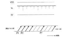
ここで、図2は、バッファ12の出力を各遅延ユニットDUに供給する信号ラインでの電圧レベルVLの変化を示す模式図である。なお、図中の電圧レベルVLを示す線のうち、点線はコンデンサ13が存在しない場合(従来装置)、実線はコンデンサ13が存在する場合(本発明)を示す。
Here, FIG. 2 is a schematic diagram showing a change in the voltage level VL in the signal line for supplying the output of the
図2に示すように、コンデンサ13が存在しない場合、遅延ユニットDUを構成するインバータゲート回路INVが反転動作(スイッチング動作)する毎に、インバータゲート回路INV(ひいては遅延ユニットDU)に瞬時的な動作電流が流れる。その動作電流によって、バッファ12の出力抵抗Rや配線抵抗に比例した電圧降下が生じることにより、電圧レベルVLは一時的に低下する。しかし、コンデンサ13が存在する場合、遅延ユニットDUのスイッチング動作時に、コンデンサ13から電流が供給され、その分、バッファ12を流れる電流が減少するため、出力抵抗Rの影響による電圧レベルVLの降下が軽減されることになる。
As shown in FIG. 2, when the
<効果>
以上説明したように、A/D変換回路1では、遅延ユニットDUのスイッチング動作時に、瞬時的な動作電流が流れても、コンデンサ13が必要な電流を供給することによって、バッファ12の出力抵抗Rやバッファ12の入力側の配線抵抗には、殆ど電流がながれないため、遅延ユニットDUに供給される電圧レベルVLの降下が大幅に軽減される。
<Effect>
As described above, in the A /
その結果、A/D変換回路1によれば、各遅延ユニットDUの遅延を精度よく均一にすることができ、分解能のバラツキが小さく精度の良いA/D変換データDTを生成することができる。
As a result, according to the A /
また、A/D変換回路1では、コンデンサ13の容量分Cが、バッファ12の抵抗分Rと共にローパスフィルタを形成し、入力信号Vinの許容最大周波数より周波数の高いノイズ成分をカットするように設定されているため、A/D変換データDTからノイズ成分の影響(誤差)を除去することができる。
Further, in the A /
更に、A/D変換回路1では、パルス遅延回路10を構成するトランジスタのサイズが、他の部分(ラッチ&エンコーダ11)を構成するトランジスタのサイズより大きいため、製造時に加工誤差が生じたり微細ゴミが付着したりする等しても、パルス遅延回路10を構成するトランジスタでは、ゲートのパターン面積が設計値から外れてしまう割合が小さく、設計した所望の特性(駆動能力等)を得ることができる。
Further, in the A /
その結果、遅延特性が均一な遅延ユニットDUを製造することができ、上述の電圧レベルVLの降下に対する対策(コンデンサ13)との相乗効果によって、より一層、A/D変換データDTの分解能のバラツキ、即ち微分非直線製誤差(DNL)を小さくすることができ、更には、製造時の歩留まりも向上させることができる。 As a result, a delay unit DU having a uniform delay characteristic can be manufactured, and the resolution of the A / D conversion data DT is further varied due to a synergistic effect with the above-described countermeasure against the drop in the voltage level VL (capacitor 13). That is, the differential non-linear manufacturing error (DNL) can be reduced, and further, the manufacturing yield can be improved.
また、パルス遅延回路10は、ラッチ&エンコーダ11と比較して、A/D変換回路1全体の中で占める回路規模が小さいため、パルス遅延回路10を構成するトランジスタのサイズを大きくしても、A/D変換回路1全体から見れば、回路規模の増大を極めて小さく抑えることができる。
[第2実施形態]
次に、第2実施形態について説明する。
Further, the
[Second Embodiment]
Next, a second embodiment will be described.
図3は、本実施形態のA/D変換回路3の全体構成図である。
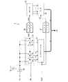
図3に示すように、A/D変換回路3は、パルス信号PAを所定の遅延時間だけ遅延させて出力するM(=2a :aは正整数)個の遅延ユニットDUをリング状に連結することにより、パルス信号PAを周回させることができるリングディレイライン(RDL)として構成されたパルス遅延回路30と、サンプリングクロックCKSの立ち上がりタイミングで、パルス遅延回路30内でのパルス信号PAの到達位置を検出(ラッチ)し、その検出結果を、パルス信号PAが通過した遅延ユニットDUが先頭から何段目にあるかを表すaビットのデジタルデータ(A/D変換データ)に変換して出力するラッチ&エンコーダ31とを備えている。
FIG. 3 is an overall configuration diagram of the A /
As shown in FIG. 3, the A /
なお、パルス遅延回路30は、初段の遅延ユニットDUは、一方の入力端子を起動用端子とするアンドゲート回路にて構成され、初段以外の他の遅延ユニットDUは、第1実施形態のものと同様に構成されている。そして、初段の遅延ユニットDUの起動用端子とは異なるもう一つの入力端子と、最終段の遅延ユニットDUの出力端子とを接続することでリング状にされている。また、パルス遅延回路30は、図示しないが、パルス遅延回路30内でのパルス信号の周回が継続して行われるように、初段の遅延ユニットDUの入力端子の信号レベルを操作するように構成されている。このようなパルス遅延回路30の具体的な構成は、例えば、特開平6−216721号等に詳述されているため、ここではその詳細についての説明を省略する。
In the
そして、各遅延ユニットDUには、バッファ32を介して、A/D変換対象となる入力信号Vinが駆動電圧として印加されている。従って、各遅延ユニットDUの遅延時間は、入力信号Vinの電圧レベルに対応した時間となり、サンプリングクロックCKSの一周期、即ちサンプリング周期(測定時間)TS内にパルス遅延回路30内でのパルス信号PAが通過する遅延ユニットDUの段数は、入力信号Vinの電圧レベル(測定時間TSの間の平均電圧レベル)に比例したものとなる。
An input signal Vin to be A / D converted is applied as a drive voltage to each delay unit DU via the
また、バッファ32の出力を各遅延ユニットDUに供給する信号ラインとグランドラインとの間には、コンデンサ33が設けられている。但し、バッファ32の出力抵抗をR、コンデンサ33の容量をCとして、これらR,Cから算出される時定数が、入力信号Vinとして許容される信号成分の最大周波数の逆数(最大周波数となる信号成分の1波長分の周期)より小さな値となるように、コンデンサ33の容量Cは設定されている。
A
また、A/D変換回路3は、動作クロックCKAに従ってカウント動作するb(bは正整数)ビットの同期式カウンタからなる周回数カウンタ36と、周回数カウンタ36によるカウント値をラッチパルスLPの立ち上がりタイミングでラッチするラッチ回路38と、パルス遅延回路30を構成する最終段の遅延ユニットDUの出力(周回クロック)CKCを入力とし、出力を動作クロックCKAとして周回数カウンタ36に供給する駆動用バッファ回路35と、サンプリングクロックCKSを入力とし、出力をラッチパルスLPとしてラッチ回路38に供給する遅延用バッファ回路37とを備えている。
Further, the A /
なお、駆動用バッファ回路35は、CMOSインバータゲート回路を複数段直列接続してなり、その最終段のインバータゲート回路は、周回数カウンタ36のクロックラインの入力容量に対して十分な駆動能力を有する大きさに構成され、他のインバータゲート回路は、初段から最終段に向けて段階的に駆動能力が大きくなるように構成されている。
The driving
また、遅延用バッファ回路37は、駆動用バッファ回路35と同様に構成されており、駆動用バッファ回路35での遅延時間と遅延用バッファ回路37での遅延時間とが等しくなるようにされている。
The
ところで、A/D変換回路3は、第1実施形態のものと同様に、コンデンサ33も含めた全ての部位が、CMOS製造プロセスを使用して半導体基板(ICチップ)上の半導体集積回路として構成される。
By the way, the A /
そして、A/D変換回路3のうち、ラッチ&エンコーダ31,周回数カウンタ36,ラッチ回路38は、当該半導体集積回路に適用するCMOSデジタル回路設計ルールの最小サイズで設計されたトランジスタを用いて構成されている。また、各遅延ユニットDUでの遅延を均一にすべきパルス遅延回路30、及び互いの遅延を同一にすべき駆動用バッファ回路35と遅延用バッファ回路37は、ラッチ&エンコーダ31,周回数カウンタ36,ラッチ回路38を構成するトランジスタより大きなサイズに設計されたトランジスタを用いて構成されている。
In the A /
また、バッファ32やコンデンサ33は、バッファ32の出力抵抗及びバッファ32の出力から各遅延ユニットDUに至る信号ラインの配線抵抗の合計が、遅延ユニットDUのオン抵抗に対して1/10程度(望ましくは1/100程度)となるように配置されている。具体的には、パルス遅延回路30から1mm(望ましくは100μm)以内に配置されている。
In the
<動作>
このように構成されたA/D変換回路3では、ラッチ&エンコーダ31は、第1実施形態におけるラッチ&エンコーダ11と同様に動作する。周回数カウンタ36は、動作クロックCKAに従って、パルス遅延回路30内でのパルス信号PAの周回回数をカウントし、ラッチ回路38は、ラッチパルスLPに従って、周回数カウンタ36のカウント値をラッチする。
<Operation>
In the A /
また、周回数カウンタ36は、駆動用バッファ回路35を介して動作クロックCKAが供給されるため、周回数カウンタ36のビット数が多く、クロックラインの入力容量が大きい場合でも、安定した動作をする。
In addition, since the operation clock CKA is supplied to the
但し、周回数カウンタ36の動作は、動作クロックCKAが駆動用バッファ回路35にて遅延する分だけ、パルス遅延回路30が出力する周回クロックCKCのタイミングより遅れ、また、ラッチ回路38の動作も、ラッチパルスLPが遅延用バッファ回路37にて遅延する分だけ、サンプリングクロックCKSのタイミングより遅れる。
However, the operation of the
つまり、周回数カウンタ36の動作が遅れる分だけ、カウント値のラッチタイミングも遅らせることにより、ラッチ回路38がラッチパルスLPに従って周回数カウンタ36のカウント値をラッチするタイミングと、ラッチ&エンコーダ31が、サンプリングクロックCKSに従って、パルス遅延回路30からの遅延パルス(各遅延ユニットDUの出力)をラッチするタイミングとの整合がとれるようにされている。
That is, by delaying the latch timing of the count value by the delay of the operation of the
そして、パルス信号PAと、このパルス信号PAの入力後、予め設定されたサンプリング周期TSが経過した時点で立ち上がるサンプリングクロックCKSとが入力されたA/D変換回路3は、ラッチ&エンコーダ31から出力されるaビットのデジタルデータを、入力信号Vinの電圧レベルを表す下位ビットデータ、ラッチ回路38から出力されるbビットのカウント値を、入力信号Vinの電圧レベルを表す上位ビットデータとするa+bビットのデジタルデータ(A/D変換データ)DTを出力する。
The A /
<効果>
このように構成されたA/D変換回路3では、バッファ32の出力を各遅延ユニットDUに供給する信号ラインとグランドラインとの間にコンデンサ33が設けられているため、第1実施形態のA/D変換回路1と同様の効果を得ることができる。
<Effect>
In the A /
また、A/D変換回路3では、パルス遅延回路30としてリングディレイラインを使用し、パルス遅延回路30でのパルス信号PAの周回数を周回数カウンタ36でカウントするようにされているため、パルス遅延回路30を構成する遅延ユニットDUの段数を大幅に削減でき、回路規模を削減することができる。
In the A /
また、A/D変換回路3では、パルス遅延回路30,駆動用バッファ回路35,遅延用バッファ回路37を構成するトランジスタのサイズが、他の部分(ラッチ&エンコーダ31,周回数カウンタ36,ラッチ回路38)より大きいため、製造時に加工誤差が生じたり微細ゴミが付着する等したとしても、パルス遅延回路30,駆動用バッファ回路35,遅延用バッファ回路37を構成するトランジスタでは、ゲートのパターン面積が設計値から外れてしまう割合が小さく、設計した所望の特性を得ることができる。
In the A /
その結果、遅延特性が均一な遅延ユニットDUを製造することができ、上述の電圧レベルVLの降下に対する対策(コンデンサ33)との相乗効果によって、A/D変換データの分解能のバラツキ、即ち微分非直線製誤差(DNL)を小さくすることができると共に、駆動用バッファ回路35と遅延用バッファ回路37の遅延も精度よく一致するため、A/D変換データの上位ビットと下位ビットとの整合性も確保することができ、更には、製造時の歩留まりも向上させることができる。
[第3実施形態]
次に、第3実施形態について説明する。
As a result, a delay unit DU having a uniform delay characteristic can be manufactured, and due to a synergistic effect with the above-described countermeasure against the drop in the voltage level VL (capacitor 33), variation in resolution of A / D conversion data, that is, non-differentiation The straight line error (DNL) can be reduced, and the delays of the
[Third Embodiment]
Next, a third embodiment will be described.
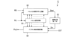
図1は、外部から入力される基準信号PBを分周又は逓倍して所定周波数の出力信号(パルス信号)Pout を生成する、周波数変換装置5の全体構成図である。
Figure 1 generates an output signal (pulse signal) P out of a predetermined frequency reference signal PB input from the outside by dividing or multiplying an overall configuration diagram of a
図1に示すように、周波数変換装置5は、リング状に連結した多数の遅延ユニットからなり、外部から制御信号PAが入力されているときに各遅延ユニットがパルス信号を順次遅延させて周回させるリングオシレータとして構成されたパルス遅延回路51と、このパルス遅延回路51を構成する各遅延ユニットから順次出力される遅延信号に基づき、基準信号PBの立ち上がりから次の立ち上がりまでの位相差(つまり周期)を2進デジタル値Dout に変換するパルス位相差符号化回路52と、このパルス位相差符号化回路52にて得られた2進デジタル値Dout に所定値を乗・除してパルス信号Pout の出力周期を表わす制御データDinを生成する演算回路53と、この演算回路53から出力される制御データDinとパルス遅延回路51から順次出力される遅延信号とに基づき、基準信号PBを分周又は逓倍した周期でパルス信号Pout を出力するデジタル制御発振回路54とを備え、パルス位相差符号化装置と発振装置との複合装置として構成されている。
As shown in FIG. 1, the
なお、パルス遅延回路51は、第2実施形態におけるパルス遅延回路30,バッファ32,コンデンサ33と同様に構成されている。
The
また、パルス位相差符号化回路52,演算回路53,デジタル制御発振回路54は、例えば、特開平7−183800号公報に詳述された周知のものであるため、ここでは説明を省略する。
Further, the pulse phase
つまり、遅延ユニットDUに対して入力信号Vinを供給する信号ラインとグランドラインとの間にコンデンサを挿入した構成は、このような周波数変換装置5等に適用してもよい。
[他の実施形態]
以上、本発明のいくつかの実施形態について説明したが、本発明は上記実施形態に限定されるものではなく、本発明の要旨を逸脱しない範囲において、様々な態様にて実施することが可能である。
That is, a configuration in which a capacitor is inserted between the signal line that supplies the input signal Vin to the delay unit DU and the ground line may be applied to such a
[Other Embodiments]
As mentioned above, although several embodiment of this invention was described, this invention is not limited to the said embodiment, In the range which does not deviate from the summary of this invention, it is possible to implement in various aspects. is there.
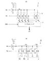
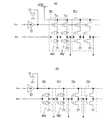
例えば、上記実施形態では、パルス遅延回路10(パルス遅延回路30も同様)を構成する遅延ユニットDUを、Pチャネルトランジスタ(FET)とNチャネルトランジスタ(FET)とからなるCMOSインバータゲート回路INVを2段直列接続することで構成し、入力信号Vinを駆動電圧として各遅延ユニットDUに印加するものとして説明したが、図5(a)に示すように、遅延ユニットDUを構成する各CMOSインバータゲート回路INVに、駆動電流を外部から制御するための制御トランジスタ(FET)Trcが設けられている場合には、この制御トランジスタの制御端子(ゲート)に、制御信号として、入力信号Vinを入力するようにしてもよい。但し、この場合、入力信号Vinを各遅延ユニットDUの制御トランジスタTrcに供給する信号ラインにバッファ12(32),コンデンサ13(33)を接続する。 For example, in the above embodiment, the delay unit DU constituting the pulse delay circuit 10 (the same applies to the pulse delay circuit 30) is replaced by two CMOS inverter gate circuits INV each composed of a P-channel transistor (FET) and an N-channel transistor (FET). Although it is described that the input signal Vin is applied to each delay unit DU as a drive voltage by being connected in stages, as shown in FIG. 5A, each CMOS inverter gate circuit that constitutes the delay unit DU. When the control transistor (FET) Trc for controlling the drive current from the outside is provided in the INV, the input signal Vin is input as a control signal to the control terminal (gate) of the control transistor. May be. However, in this case, the buffer 12 (32) and the capacitor 13 (33) are connected to a signal line for supplying the input signal Vin to the control transistor Trc of each delay unit DU.
つまり、インバータINV等のゲート回路は、直流電源から供給される駆動電流によっても、その動作時間が変化することから、その駆動電流を入力信号Vinに基づき制御するようにしても、上記と同様の効果を得ることができる。 In other words, since the operation time of the gate circuit such as the inverter INV changes depending on the drive current supplied from the DC power supply, the drive current is controlled based on the input signal Vin. An effect can be obtained.
また、この場合、入力信号Vinの対する遅延ユニットDUの入力インピーダンスが高くなるため、バッファ12(32)を省略してもよい。 In this case, the input impedance of the delay unit DU with respect to the input signal Vin becomes high, and therefore the buffer 12 (32) may be omitted.
また、パルス遅延回路10,30を構成する遅延ユニットDUは、必ずしも2段のインバータゲート回路INVで実現する必要はなく、図5(b)に示すように、1段のインバータゲート回路INVで実現してもよいし、3段以上のインバータゲート回路で実現してもよい。
Further, the delay unit DU constituting the
更に、遅延ユニットDUは、必ずしもインバータゲート回路INVで実現する必要はなく、AND,OR,NAND,NOR等の論理回路の標準セルを用いて実現してもよい。 Further, the delay unit DU is not necessarily realized by the inverter gate circuit INV, but may be realized by using a standard cell of a logic circuit such as AND, OR, NAND, NOR.
また、バッファ12,32としては、単なる抵抗器を用いてもよい。
As the
1,3…A/D変換回路 5…周波数変換装置 10,30,51…パルス遅延回路 11,31…エンコーダ 12,32…バッファ 13,33…コンデンサ 35…駆動用バッファ回路 36…周回数カウンタ 37…遅延用バッファ回路 38…ラッチ回路 52…パルス位相差符号化回路 53…演算回路 54…デジタル制御発振回路 DU…遅延ユニット INV…CMOSインバータゲート回路 Trc…制御トランジスタ
DESCRIPTION OF
Claims (10)
前記入力信号を前記遅延ユニットに供給する信号ラインに、前記遅延ユニットの反転動作時に消費される電力の供給源となる容量素子を設けたことを特徴とするパルス遅延回路。 A pulse delay that connects a plurality of delay units that delay the pulse signal with a delay time corresponding to the voltage level of the input signal in series or in a ring shape, and transmits the pulse signal while sequentially delaying it according to the delay time of each delay unit. In the circuit
A pulse delay circuit, wherein a capacitive element serving as a supply source of electric power consumed during an inversion operation of the delay unit is provided in a signal line for supplying the input signal to the delay unit.
予め設定された測定時間の間に前記パルス遅延回路内で前記パルス信号が通過した前記遅延ユニットの段数に対応する数値データを生成する符号化回路と、
を備え、前記符号化回路が生成する前記数値データを前記入力信号の電圧レベルを表すA/D変換データとして出力することを特徴とするA/D変換回路。 A pulse delay circuit according to any one of claims 1 to 8,
An encoding circuit for generating numerical data corresponding to the number of stages of the delay unit through which the pulse signal has passed in the pulse delay circuit during a preset measurement time;
And outputting the numerical data generated by the encoding circuit as A / D conversion data representing the voltage level of the input signal.
前記符号化回路は、
前記パルス遅延回路を前記パルス信号が周回した回数をカウントする周回数カウンタと、
前記パルス遅延回路内での前記パルス信号の位置を符号化した値を前記数値データの下位ビットとして出力する下位符号化回路と、
前記周回数カウンタのカウント値を前記数値データの上位ビットとして出力する上位符号化回路と、
を備えることを特徴とする請求項8又は請求項9に記載のA/D変換回路。 The pulse delay circuit comprises a ring delay line formed by connecting the delay units in a ring shape,
The encoding circuit includes:
A lap counter that counts the number of times the pulse signal circulates in the pulse delay circuit;
A low-order encoding circuit that outputs a value obtained by encoding the position of the pulse signal in the pulse delay circuit as a low-order bit of the numerical data;
An upper encoding circuit for outputting the count value of the circulation counter as upper bits of the numerical data;
The A / D conversion circuit according to claim 8, further comprising:
Priority Applications (3)
| Application Number | Priority Date | Filing Date | Title |
|---|---|---|---|
| JP2008316969A JP4645734B2 (en) | 2008-12-12 | 2008-12-12 | Pulse delay circuit and A / D conversion circuit |
| DE102009047452.8A DE102009047452B4 (en) | 2008-12-12 | 2009-12-03 | Pulse delay circuit and A/D converters featuring pulse delay circuits |
| US12/653,186 US7932848B2 (en) | 2008-12-12 | 2009-12-09 | Pulse delay circuit and A/D converter including same |
Applications Claiming Priority (1)
| Application Number | Priority Date | Filing Date | Title |
|---|---|---|---|
| JP2008316969A JP4645734B2 (en) | 2008-12-12 | 2008-12-12 | Pulse delay circuit and A / D conversion circuit |
Publications (2)
| Publication Number | Publication Date |
|---|---|
| JP2010141685A true JP2010141685A (en) | 2010-06-24 |
| JP4645734B2 JP4645734B2 (en) | 2011-03-09 |
Family
ID=42168877
Family Applications (1)
| Application Number | Title | Priority Date | Filing Date |
|---|---|---|---|
| JP2008316969A Active JP4645734B2 (en) | 2008-12-12 | 2008-12-12 | Pulse delay circuit and A / D conversion circuit |
Country Status (3)
| Country | Link |
|---|---|
| US (1) | US7932848B2 (en) |
| JP (1) | JP4645734B2 (en) |
| DE (1) | DE102009047452B4 (en) |
Cited By (2)
| Publication number | Priority date | Publication date | Assignee | Title |
|---|---|---|---|---|
| WO2012002492A1 (en) * | 2010-07-02 | 2012-01-05 | オリンパス株式会社 | Signal transfer circuit and image pickup device |
| US8779343B2 (en) | 2011-01-11 | 2014-07-15 | Olympus Corporation | Solid state image pickup device having an analog signal processing unit including first and second capacitors, a delay circuit and an A/D converting circuit for an image capturing signal process |
Families Citing this family (3)
| Publication number | Priority date | Publication date | Assignee | Title |
|---|---|---|---|---|
| KR101123353B1 (en) | 2011-09-21 | 2012-03-13 | 홍익대학교 산학협력단 | Delay-locked loop utilizing feedback delay elements |
| US8766682B2 (en) * | 2012-01-24 | 2014-07-01 | Voxtel, Inc. | Method and device for measuring duration of a time interval |
| US11526153B2 (en) | 2020-11-09 | 2022-12-13 | Analog Devices, Inc. | Programmable delay line with glitch suppression |
Citations (5)
| Publication number | Priority date | Publication date | Assignee | Title |
|---|---|---|---|---|
| JP2003032113A (en) * | 2001-07-13 | 2003-01-31 | Denso Corp | A / D conversion method and device |
| JP2003046390A (en) * | 2001-07-31 | 2003-02-14 | Denso Corp | Filtering method and A / D converter having filter function |
| JP2005322327A (en) * | 2004-05-10 | 2005-11-17 | Denso Corp | Sample hold circuit |
| JP2007134786A (en) * | 2005-11-08 | 2007-05-31 | Denso Corp | A / D conversion circuit |
| JP2007312288A (en) * | 2006-05-22 | 2007-11-29 | Denso Corp | A / D conversion circuit |
Family Cites Families (10)
| Publication number | Priority date | Publication date | Assignee | Title |
|---|---|---|---|---|
| JP3064644B2 (en) | 1992-03-16 | 2000-07-12 | 株式会社デンソー | A / D conversion circuit |
| JP3455982B2 (en) | 1993-01-14 | 2003-10-14 | 株式会社デンソー | Even stage ring oscillator and pulse phase difference encoding circuit |
| JP2900772B2 (en) | 1993-12-24 | 1999-06-02 | 株式会社デンソー | Composite device of pulse phase difference encoding circuit and pulse generation circuit and digital control PLL device |
| US6928128B1 (en) * | 1999-05-03 | 2005-08-09 | Rambus Inc. | Clock alignment circuit having a self regulating voltage supply |
| JP3956847B2 (en) | 2002-04-24 | 2007-08-08 | 株式会社デンソー | A / D conversion method and apparatus |
| JP3960267B2 (en) | 2003-05-29 | 2007-08-15 | 株式会社デンソー | A / D conversion method and apparatus |
| JP2007006369A (en) | 2005-06-27 | 2007-01-11 | Pioneer Electronic Corp | Remote controller and viewing system including the same |
| JP2007006368A (en) | 2005-06-27 | 2007-01-11 | Denso Corp | A / D conversion circuit |
| TWI312238B (en) * | 2006-04-24 | 2009-07-11 | Ind Tech Res Inst | Delay line and analog-to-digital converting apparatus and load-sensing circuit using the same |
| JP4965203B2 (en) * | 2006-09-11 | 2012-07-04 | 株式会社リコー | Delay time generation circuit, secondary battery protection semiconductor device using the same, battery pack and electronic device |
-
2008
- 2008-12-12 JP JP2008316969A patent/JP4645734B2/en active Active
-
2009
- 2009-12-03 DE DE102009047452.8A patent/DE102009047452B4/en active Active
- 2009-12-09 US US12/653,186 patent/US7932848B2/en active Active
Patent Citations (5)
| Publication number | Priority date | Publication date | Assignee | Title |
|---|---|---|---|---|
| JP2003032113A (en) * | 2001-07-13 | 2003-01-31 | Denso Corp | A / D conversion method and device |
| JP2003046390A (en) * | 2001-07-31 | 2003-02-14 | Denso Corp | Filtering method and A / D converter having filter function |
| JP2005322327A (en) * | 2004-05-10 | 2005-11-17 | Denso Corp | Sample hold circuit |
| JP2007134786A (en) * | 2005-11-08 | 2007-05-31 | Denso Corp | A / D conversion circuit |
| JP2007312288A (en) * | 2006-05-22 | 2007-11-29 | Denso Corp | A / D conversion circuit |
Cited By (4)
| Publication number | Priority date | Publication date | Assignee | Title |
|---|---|---|---|---|
| WO2012002492A1 (en) * | 2010-07-02 | 2012-01-05 | オリンパス株式会社 | Signal transfer circuit and image pickup device |
| JP2012034348A (en) * | 2010-07-02 | 2012-02-16 | Olympus Corp | Signal transfer circuit and imaging device |
| US8520796B2 (en) | 2010-07-02 | 2013-08-27 | Olympus Corporation | Signal transfer circuit and image pickup device |
| US8779343B2 (en) | 2011-01-11 | 2014-07-15 | Olympus Corporation | Solid state image pickup device having an analog signal processing unit including first and second capacitors, a delay circuit and an A/D converting circuit for an image capturing signal process |
Also Published As
| Publication number | Publication date |
|---|---|
| JP4645734B2 (en) | 2011-03-09 |
| DE102009047452B4 (en) | 2025-11-06 |
| US7932848B2 (en) | 2011-04-26 |
| DE102009047452A1 (en) | 2010-06-17 |
| US20100149016A1 (en) | 2010-06-17 |
Similar Documents
| Publication | Publication Date | Title |
|---|---|---|
| JP4396063B2 (en) | A / D conversion method and apparatus | |
| US9128146B2 (en) | Semiconductor integrated circuit | |
| JP4725418B2 (en) | Time measurement circuit | |
| JP4645734B2 (en) | Pulse delay circuit and A / D conversion circuit | |
| JP3991969B2 (en) | A / D conversion circuit | |
| JP2011223553A (en) | Amplifier circuit and analog-digital conversion circuit including amplifier circuit | |
| JP4702179B2 (en) | A / D conversion circuit | |
| JP4921329B2 (en) | A / D conversion circuit | |
| US9577661B2 (en) | Voltage-controlled oscillator and analog-digital converter | |
| US7248197B2 (en) | A/D converter that is implemented using only digital circuit components and digital signal processing | |
| JP6949669B2 (en) | TDC circuit | |
| JP6772998B2 (en) | A / D conversion circuit | |
| US7653170B2 (en) | Electrical circuit for measuring times and method for measuring times | |
| CN102017424B (en) | A/D conversion circuit | |
| JP2010246192A (en) | Power supply device, power supply device control circuit, and power supply device control method | |
| WO2008023624A1 (en) | Variable delay circuit, timing generator and semiconductor testing apparatus | |
| JP5282475B2 (en) | Trimming method of filter circuit | |
| JP4349266B2 (en) | A / D converter | |
| JP2007336119A (en) | Semiconductor device, and impedance control method | |
| JP2010283054A (en) | Process monitor circuit and method of determining process characteristics | |
| JP5564869B2 (en) | Semiconductor integrated circuit | |
| JP2715979B2 (en) | Output buffer circuit | |
| Ali et al. | Design of configurable digital spike filtering circuits in 130 nm CMOS process | |
| US8416114B2 (en) | A/D conversion circuit | |
| JPH09153802A (en) | Semiconductor integrated circuit |
Legal Events
| Date | Code | Title | Description |
|---|---|---|---|
| A621 | Written request for application examination |
Free format text: JAPANESE INTERMEDIATE CODE: A621 Effective date: 20100531 |
|
| A977 | Report on retrieval |
Free format text: JAPANESE INTERMEDIATE CODE: A971007 Effective date: 20100820 |
|
| A131 | Notification of reasons for refusal |
Free format text: JAPANESE INTERMEDIATE CODE: A131 Effective date: 20100824 |
|
| A521 | Request for written amendment filed |
Free format text: JAPANESE INTERMEDIATE CODE: A523 Effective date: 20101020 |
|
| TRDD | Decision of grant or rejection written | ||
| A01 | Written decision to grant a patent or to grant a registration (utility model) |
Free format text: JAPANESE INTERMEDIATE CODE: A01 Effective date: 20101109 |
|
| A01 | Written decision to grant a patent or to grant a registration (utility model) |
Free format text: JAPANESE INTERMEDIATE CODE: A01 |
|
| A61 | First payment of annual fees (during grant procedure) |
Free format text: JAPANESE INTERMEDIATE CODE: A61 Effective date: 20101122 |
|
| FPAY | Renewal fee payment (event date is renewal date of database) |
Free format text: PAYMENT UNTIL: 20131217 Year of fee payment: 3 |
|
| R151 | Written notification of patent or utility model registration |
Ref document number: 4645734 Country of ref document: JP Free format text: JAPANESE INTERMEDIATE CODE: R151 |
|
| FPAY | Renewal fee payment (event date is renewal date of database) |
Free format text: PAYMENT UNTIL: 20131217 Year of fee payment: 3 |
|
| R250 | Receipt of annual fees |
Free format text: JAPANESE INTERMEDIATE CODE: R250 |
|
| R250 | Receipt of annual fees |
Free format text: JAPANESE INTERMEDIATE CODE: R250 |
|
| R250 | Receipt of annual fees |
Free format text: JAPANESE INTERMEDIATE CODE: R250 |
|
| R250 | Receipt of annual fees |
Free format text: JAPANESE INTERMEDIATE CODE: R250 |
|
| R250 | Receipt of annual fees |
Free format text: JAPANESE INTERMEDIATE CODE: R250 |
|
| R250 | Receipt of annual fees |
Free format text: JAPANESE INTERMEDIATE CODE: R250 |
|
| R250 | Receipt of annual fees |
Free format text: JAPANESE INTERMEDIATE CODE: R250 |
|
| R250 | Receipt of annual fees |
Free format text: JAPANESE INTERMEDIATE CODE: R250 |
|
| R250 | Receipt of annual fees |
Free format text: JAPANESE INTERMEDIATE CODE: R250 |
|
| R250 | Receipt of annual fees |
Free format text: JAPANESE INTERMEDIATE CODE: R250 |
|
| R250 | Receipt of annual fees |
Free format text: JAPANESE INTERMEDIATE CODE: R250 |
|
| R250 | Receipt of annual fees |
Free format text: JAPANESE INTERMEDIATE CODE: R250 |