JP2010141055A - 半導体モジュール、半導体モジュールの製造方法および携帯機器 - Google Patents
半導体モジュール、半導体モジュールの製造方法および携帯機器 Download PDFInfo
- Publication number
- JP2010141055A JP2010141055A JP2008314960A JP2008314960A JP2010141055A JP 2010141055 A JP2010141055 A JP 2010141055A JP 2008314960 A JP2008314960 A JP 2008314960A JP 2008314960 A JP2008314960 A JP 2008314960A JP 2010141055 A JP2010141055 A JP 2010141055A
- Authority
- JP
- Japan
- Prior art keywords
- electrode
- substrate
- semiconductor module
- semiconductor
- width
- Prior art date
- Legal status (The legal status is an assumption and is not a legal conclusion. Google has not performed a legal analysis and makes no representation as to the accuracy of the status listed.)
- Withdrawn
Links
Images


Classifications
-
- H—ELECTRICITY
- H10—SEMICONDUCTOR DEVICES; ELECTRIC SOLID-STATE DEVICES NOT OTHERWISE PROVIDED FOR
- H10W—GENERIC PACKAGES, INTERCONNECTIONS, CONNECTORS OR OTHER CONSTRUCTIONAL DETAILS OF DEVICES COVERED BY CLASS H10
- H10W70/00—Package substrates; Interposers; Redistribution layers [RDL]
- H10W70/60—Insulating or insulated package substrates; Interposers; Redistribution layers
- H10W70/62—Insulating or insulated package substrates; Interposers; Redistribution layers characterised by their interconnections
- H10W70/65—Shapes or dispositions of interconnections
-
- H—ELECTRICITY
- H05—ELECTRIC TECHNIQUES NOT OTHERWISE PROVIDED FOR
- H05K—PRINTED CIRCUITS; CASINGS OR CONSTRUCTIONAL DETAILS OF ELECTRIC APPARATUS; MANUFACTURE OF ASSEMBLAGES OF ELECTRICAL COMPONENTS
- H05K1/00—Printed circuits
- H05K1/18—Printed circuits structurally associated with non-printed electric components
- H05K1/182—Printed circuits structurally associated with non-printed electric components associated with components mounted in printed circuit boards [PCB], e.g. insert-mounted components [IMC]
- H05K1/185—Printed circuits structurally associated with non-printed electric components associated with components mounted in printed circuit boards [PCB], e.g. insert-mounted components [IMC] associated with components encapsulated in the insulating substrate of the PCBs; associated with components incorporated in internal layers of multilayer circuit boards
-
- H—ELECTRICITY
- H05—ELECTRIC TECHNIQUES NOT OTHERWISE PROVIDED FOR
- H05K—PRINTED CIRCUITS; CASINGS OR CONSTRUCTIONAL DETAILS OF ELECTRIC APPARATUS; MANUFACTURE OF ASSEMBLAGES OF ELECTRICAL COMPONENTS
- H05K3/00—Apparatus or processes for manufacturing printed circuits
- H05K3/30—Assembling printed circuits with electric components, e.g. with resistors
- H05K3/32—Assembling printed circuits with electric components, e.g. with resistors electrically connecting electric components or wires to printed circuits
- H05K3/34—Assembling printed circuits with electric components, e.g. with resistors electrically connecting electric components or wires to printed circuits by soldering
- H05K3/341—Surface mounted components
- H05K3/3431—Leadless components
- H05K3/3436—Leadless components having an array of bottom contacts, e.g. pad grid array or ball grid array components
-
- H—ELECTRICITY
- H10—SEMICONDUCTOR DEVICES; ELECTRIC SOLID-STATE DEVICES NOT OTHERWISE PROVIDED FOR
- H10W—GENERIC PACKAGES, INTERCONNECTIONS, CONNECTORS OR OTHER CONSTRUCTIONAL DETAILS OF DEVICES COVERED BY CLASS H10
- H10W70/00—Package substrates; Interposers; Redistribution layers [RDL]
- H10W70/60—Insulating or insulated package substrates; Interposers; Redistribution layers
- H10W70/62—Insulating or insulated package substrates; Interposers; Redistribution layers characterised by their interconnections
- H10W70/63—Vias, e.g. via plugs
- H10W70/635—Through-vias
-
- H—ELECTRICITY
- H10—SEMICONDUCTOR DEVICES; ELECTRIC SOLID-STATE DEVICES NOT OTHERWISE PROVIDED FOR
- H10W—GENERIC PACKAGES, INTERCONNECTIONS, CONNECTORS OR OTHER CONSTRUCTIONAL DETAILS OF DEVICES COVERED BY CLASS H10
- H10W74/00—Encapsulations, e.g. protective coatings
- H10W74/01—Manufacture or treatment
- H10W74/012—Manufacture or treatment of encapsulations on active surfaces of flip-chip devices, e.g. forming underfills
-
- H—ELECTRICITY
- H10—SEMICONDUCTOR DEVICES; ELECTRIC SOLID-STATE DEVICES NOT OTHERWISE PROVIDED FOR
- H10W—GENERIC PACKAGES, INTERCONNECTIONS, CONNECTORS OR OTHER CONSTRUCTIONAL DETAILS OF DEVICES COVERED BY CLASS H10
- H10W74/00—Encapsulations, e.g. protective coatings
- H10W74/10—Encapsulations, e.g. protective coatings characterised by their shape or disposition
- H10W74/111—Encapsulations, e.g. protective coatings characterised by their shape or disposition the semiconductor body being completely enclosed
- H10W74/129—Encapsulations, e.g. protective coatings characterised by their shape or disposition the semiconductor body being completely enclosed forming a chip-scale package [CSP]
-
- H—ELECTRICITY
- H10—SEMICONDUCTOR DEVICES; ELECTRIC SOLID-STATE DEVICES NOT OTHERWISE PROVIDED FOR
- H10W—GENERIC PACKAGES, INTERCONNECTIONS, CONNECTORS OR OTHER CONSTRUCTIONAL DETAILS OF DEVICES COVERED BY CLASS H10
- H10W74/00—Encapsulations, e.g. protective coatings
- H10W74/10—Encapsulations, e.g. protective coatings characterised by their shape or disposition
- H10W74/15—Encapsulations, e.g. protective coatings characterised by their shape or disposition on active surfaces of flip-chip devices, e.g. underfills
-
- H—ELECTRICITY
- H10—SEMICONDUCTOR DEVICES; ELECTRIC SOLID-STATE DEVICES NOT OTHERWISE PROVIDED FOR
- H10W—GENERIC PACKAGES, INTERCONNECTIONS, CONNECTORS OR OTHER CONSTRUCTIONAL DETAILS OF DEVICES COVERED BY CLASS H10
- H10W90/00—Package configurations
- H10W90/701—Package configurations characterised by the relative positions of pads or connectors relative to package parts
-
- H—ELECTRICITY
- H05—ELECTRIC TECHNIQUES NOT OTHERWISE PROVIDED FOR
- H05K—PRINTED CIRCUITS; CASINGS OR CONSTRUCTIONAL DETAILS OF ELECTRIC APPARATUS; MANUFACTURE OF ASSEMBLAGES OF ELECTRICAL COMPONENTS
- H05K1/00—Printed circuits
- H05K1/02—Details
- H05K1/11—Printed elements for providing electric connections to or between printed circuits
- H05K1/111—Pads for surface mounting, e.g. lay-out
-
- H—ELECTRICITY
- H05—ELECTRIC TECHNIQUES NOT OTHERWISE PROVIDED FOR
- H05K—PRINTED CIRCUITS; CASINGS OR CONSTRUCTIONAL DETAILS OF ELECTRIC APPARATUS; MANUFACTURE OF ASSEMBLAGES OF ELECTRICAL COMPONENTS
- H05K2201/00—Indexing scheme relating to printed circuits covered by H05K1/00
- H05K2201/09—Shape and layout
- H05K2201/09209—Shape and layout details of conductors
- H05K2201/09372—Pads and lands
- H05K2201/09427—Special relation between the location or dimension of a pad or land and the location or dimension of a terminal
-
- H—ELECTRICITY
- H05—ELECTRIC TECHNIQUES NOT OTHERWISE PROVIDED FOR
- H05K—PRINTED CIRCUITS; CASINGS OR CONSTRUCTIONAL DETAILS OF ELECTRIC APPARATUS; MANUFACTURE OF ASSEMBLAGES OF ELECTRICAL COMPONENTS
- H05K2201/00—Indexing scheme relating to printed circuits covered by H05K1/00
- H05K2201/10—Details of components or other objects attached to or integrated in a printed circuit board
- H05K2201/10613—Details of electrical connections of non-printed components, e.g. special leads
- H05K2201/10621—Components characterised by their electrical contacts
- H05K2201/10674—Flip chip
-
- H—ELECTRICITY
- H05—ELECTRIC TECHNIQUES NOT OTHERWISE PROVIDED FOR
- H05K—PRINTED CIRCUITS; CASINGS OR CONSTRUCTIONAL DETAILS OF ELECTRIC APPARATUS; MANUFACTURE OF ASSEMBLAGES OF ELECTRICAL COMPONENTS
- H05K2201/00—Indexing scheme relating to printed circuits covered by H05K1/00
- H05K2201/10—Details of components or other objects attached to or integrated in a printed circuit board
- H05K2201/10613—Details of electrical connections of non-printed components, e.g. special leads
- H05K2201/10954—Other details of electrical connections
- H05K2201/10977—Encapsulated connections
-
- H—ELECTRICITY
- H10—SEMICONDUCTOR DEVICES; ELECTRIC SOLID-STATE DEVICES NOT OTHERWISE PROVIDED FOR
- H10W—GENERIC PACKAGES, INTERCONNECTIONS, CONNECTORS OR OTHER CONSTRUCTIONAL DETAILS OF DEVICES COVERED BY CLASS H10
- H10W70/00—Package substrates; Interposers; Redistribution layers [RDL]
- H10W70/01—Manufacture or treatment
- H10W70/05—Manufacture or treatment of insulating or insulated package substrates, or of interposers, or of redistribution layers
-
- H—ELECTRICITY
- H10—SEMICONDUCTOR DEVICES; ELECTRIC SOLID-STATE DEVICES NOT OTHERWISE PROVIDED FOR
- H10W—GENERIC PACKAGES, INTERCONNECTIONS, CONNECTORS OR OTHER CONSTRUCTIONAL DETAILS OF DEVICES COVERED BY CLASS H10
- H10W70/00—Package substrates; Interposers; Redistribution layers [RDL]
- H10W70/60—Insulating or insulated package substrates; Interposers; Redistribution layers
- H10W70/62—Insulating or insulated package substrates; Interposers; Redistribution layers characterised by their interconnections
- H10W70/65—Shapes or dispositions of interconnections
- H10W70/652—Cross-sectional shapes
-
- H—ELECTRICITY
- H10—SEMICONDUCTOR DEVICES; ELECTRIC SOLID-STATE DEVICES NOT OTHERWISE PROVIDED FOR
- H10W—GENERIC PACKAGES, INTERCONNECTIONS, CONNECTORS OR OTHER CONSTRUCTIONAL DETAILS OF DEVICES COVERED BY CLASS H10
- H10W70/00—Package substrates; Interposers; Redistribution layers [RDL]
- H10W70/60—Insulating or insulated package substrates; Interposers; Redistribution layers
- H10W70/62—Insulating or insulated package substrates; Interposers; Redistribution layers characterised by their interconnections
- H10W70/65—Shapes or dispositions of interconnections
- H10W70/654—Top-view layouts
- H10W70/655—Fan-out layouts
-
- H—ELECTRICITY
- H10—SEMICONDUCTOR DEVICES; ELECTRIC SOLID-STATE DEVICES NOT OTHERWISE PROVIDED FOR
- H10W—GENERIC PACKAGES, INTERCONNECTIONS, CONNECTORS OR OTHER CONSTRUCTIONAL DETAILS OF DEVICES COVERED BY CLASS H10
- H10W70/00—Package substrates; Interposers; Redistribution layers [RDL]
- H10W70/60—Insulating or insulated package substrates; Interposers; Redistribution layers
- H10W70/62—Insulating or insulated package substrates; Interposers; Redistribution layers characterised by their interconnections
- H10W70/66—Conductive materials thereof
-
- H—ELECTRICITY
- H10—SEMICONDUCTOR DEVICES; ELECTRIC SOLID-STATE DEVICES NOT OTHERWISE PROVIDED FOR
- H10W—GENERIC PACKAGES, INTERCONNECTIONS, CONNECTORS OR OTHER CONSTRUCTIONAL DETAILS OF DEVICES COVERED BY CLASS H10
- H10W72/00—Interconnections or connectors in packages
- H10W72/071—Connecting or disconnecting
- H10W72/072—Connecting or disconnecting of bump connectors
- H10W72/07231—Techniques
- H10W72/07236—Soldering or alloying
-
- H—ELECTRICITY
- H10—SEMICONDUCTOR DEVICES; ELECTRIC SOLID-STATE DEVICES NOT OTHERWISE PROVIDED FOR
- H10W—GENERIC PACKAGES, INTERCONNECTIONS, CONNECTORS OR OTHER CONSTRUCTIONAL DETAILS OF DEVICES COVERED BY CLASS H10
- H10W72/00—Interconnections or connectors in packages
- H10W72/071—Connecting or disconnecting
- H10W72/073—Connecting or disconnecting of die-attach connectors
-
- H—ELECTRICITY
- H10—SEMICONDUCTOR DEVICES; ELECTRIC SOLID-STATE DEVICES NOT OTHERWISE PROVIDED FOR
- H10W—GENERIC PACKAGES, INTERCONNECTIONS, CONNECTORS OR OTHER CONSTRUCTIONAL DETAILS OF DEVICES COVERED BY CLASS H10
- H10W72/00—Interconnections or connectors in packages
- H10W72/20—Bump connectors, e.g. solder bumps or copper pillars; Dummy bumps; Thermal bumps
- H10W72/221—Structures or relative sizes
- H10W72/222—Multilayered bumps, e.g. a coating on top and side surfaces of a bump core
-
- H—ELECTRICITY
- H10—SEMICONDUCTOR DEVICES; ELECTRIC SOLID-STATE DEVICES NOT OTHERWISE PROVIDED FOR
- H10W—GENERIC PACKAGES, INTERCONNECTIONS, CONNECTORS OR OTHER CONSTRUCTIONAL DETAILS OF DEVICES COVERED BY CLASS H10
- H10W72/00—Interconnections or connectors in packages
- H10W72/20—Bump connectors, e.g. solder bumps or copper pillars; Dummy bumps; Thermal bumps
- H10W72/241—Dispositions, e.g. layouts
- H10W72/242—Dispositions, e.g. layouts relative to the surface, e.g. recessed, protruding
-
- H—ELECTRICITY
- H10—SEMICONDUCTOR DEVICES; ELECTRIC SOLID-STATE DEVICES NOT OTHERWISE PROVIDED FOR
- H10W—GENERIC PACKAGES, INTERCONNECTIONS, CONNECTORS OR OTHER CONSTRUCTIONAL DETAILS OF DEVICES COVERED BY CLASS H10
- H10W72/00—Interconnections or connectors in packages
- H10W72/20—Bump connectors, e.g. solder bumps or copper pillars; Dummy bumps; Thermal bumps
- H10W72/241—Dispositions, e.g. layouts
- H10W72/244—Dispositions, e.g. layouts relative to underlying supporting features, e.g. bond pads, RDLs or vias
-
- H—ELECTRICITY
- H10—SEMICONDUCTOR DEVICES; ELECTRIC SOLID-STATE DEVICES NOT OTHERWISE PROVIDED FOR
- H10W—GENERIC PACKAGES, INTERCONNECTIONS, CONNECTORS OR OTHER CONSTRUCTIONAL DETAILS OF DEVICES COVERED BY CLASS H10
- H10W72/00—Interconnections or connectors in packages
- H10W72/20—Bump connectors, e.g. solder bumps or copper pillars; Dummy bumps; Thermal bumps
- H10W72/251—Materials
- H10W72/252—Materials comprising solid metals or solid metalloids, e.g. PbSn, Ag or Cu
-
- H—ELECTRICITY
- H10—SEMICONDUCTOR DEVICES; ELECTRIC SOLID-STATE DEVICES NOT OTHERWISE PROVIDED FOR
- H10W—GENERIC PACKAGES, INTERCONNECTIONS, CONNECTORS OR OTHER CONSTRUCTIONAL DETAILS OF DEVICES COVERED BY CLASS H10
- H10W72/00—Interconnections or connectors in packages
- H10W72/20—Bump connectors, e.g. solder bumps or copper pillars; Dummy bumps; Thermal bumps
- H10W72/29—Bond pads specially adapted therefor
-
- H—ELECTRICITY
- H10—SEMICONDUCTOR DEVICES; ELECTRIC SOLID-STATE DEVICES NOT OTHERWISE PROVIDED FOR
- H10W—GENERIC PACKAGES, INTERCONNECTIONS, CONNECTORS OR OTHER CONSTRUCTIONAL DETAILS OF DEVICES COVERED BY CLASS H10
- H10W72/00—Interconnections or connectors in packages
- H10W72/30—Die-attach connectors
- H10W72/381—Auxiliary members
- H10W72/387—Flow barriers
-
- H—ELECTRICITY
- H10—SEMICONDUCTOR DEVICES; ELECTRIC SOLID-STATE DEVICES NOT OTHERWISE PROVIDED FOR
- H10W—GENERIC PACKAGES, INTERCONNECTIONS, CONNECTORS OR OTHER CONSTRUCTIONAL DETAILS OF DEVICES COVERED BY CLASS H10
- H10W72/00—Interconnections or connectors in packages
- H10W72/851—Dispositions of multiple connectors or interconnections
- H10W72/853—On the same surface
- H10W72/856—Bump connectors and die-attach connectors
-
- H—ELECTRICITY
- H10—SEMICONDUCTOR DEVICES; ELECTRIC SOLID-STATE DEVICES NOT OTHERWISE PROVIDED FOR
- H10W—GENERIC PACKAGES, INTERCONNECTIONS, CONNECTORS OR OTHER CONSTRUCTIONAL DETAILS OF DEVICES COVERED BY CLASS H10
- H10W72/00—Interconnections or connectors in packages
- H10W72/90—Bond pads, in general
- H10W72/921—Structures or relative sizes of bond pads
- H10W72/922—Bond pads being integral with underlying chip-level interconnections
-
- H—ELECTRICITY
- H10—SEMICONDUCTOR DEVICES; ELECTRIC SOLID-STATE DEVICES NOT OTHERWISE PROVIDED FOR
- H10W—GENERIC PACKAGES, INTERCONNECTIONS, CONNECTORS OR OTHER CONSTRUCTIONAL DETAILS OF DEVICES COVERED BY CLASS H10
- H10W72/00—Interconnections or connectors in packages
- H10W72/90—Bond pads, in general
- H10W72/931—Shapes of bond pads
- H10W72/934—Cross-sectional shape, i.e. in side view
-
- H—ELECTRICITY
- H10—SEMICONDUCTOR DEVICES; ELECTRIC SOLID-STATE DEVICES NOT OTHERWISE PROVIDED FOR
- H10W—GENERIC PACKAGES, INTERCONNECTIONS, CONNECTORS OR OTHER CONSTRUCTIONAL DETAILS OF DEVICES COVERED BY CLASS H10
- H10W72/00—Interconnections or connectors in packages
- H10W72/90—Bond pads, in general
- H10W72/941—Dispositions of bond pads
- H10W72/9415—Dispositions of bond pads relative to the surface, e.g. recessed, protruding
-
- H—ELECTRICITY
- H10—SEMICONDUCTOR DEVICES; ELECTRIC SOLID-STATE DEVICES NOT OTHERWISE PROVIDED FOR
- H10W—GENERIC PACKAGES, INTERCONNECTIONS, CONNECTORS OR OTHER CONSTRUCTIONAL DETAILS OF DEVICES COVERED BY CLASS H10
- H10W72/00—Interconnections or connectors in packages
- H10W72/90—Bond pads, in general
- H10W72/951—Materials of bond pads
- H10W72/952—Materials of bond pads comprising metals or metalloids, e.g. PbSn, Ag or Cu
-
- H—ELECTRICITY
- H10—SEMICONDUCTOR DEVICES; ELECTRIC SOLID-STATE DEVICES NOT OTHERWISE PROVIDED FOR
- H10W—GENERIC PACKAGES, INTERCONNECTIONS, CONNECTORS OR OTHER CONSTRUCTIONAL DETAILS OF DEVICES COVERED BY CLASS H10
- H10W90/00—Package configurations
- H10W90/701—Package configurations characterised by the relative positions of pads or connectors relative to package parts
- H10W90/721—Package configurations characterised by the relative positions of pads or connectors relative to package parts of bump connectors
- H10W90/724—Package configurations characterised by the relative positions of pads or connectors relative to package parts of bump connectors between a chip and a stacked insulating package substrate, interposer or RDL
-
- H—ELECTRICITY
- H10—SEMICONDUCTOR DEVICES; ELECTRIC SOLID-STATE DEVICES NOT OTHERWISE PROVIDED FOR
- H10W—GENERIC PACKAGES, INTERCONNECTIONS, CONNECTORS OR OTHER CONSTRUCTIONAL DETAILS OF DEVICES COVERED BY CLASS H10
- H10W90/00—Package configurations
- H10W90/701—Package configurations characterised by the relative positions of pads or connectors relative to package parts
- H10W90/731—Package configurations characterised by the relative positions of pads or connectors relative to package parts of die-attach connectors
- H10W90/734—Package configurations characterised by the relative positions of pads or connectors relative to package parts of die-attach connectors between a chip and a stacked insulating package substrate, interposer or RDL
-
- Y—GENERAL TAGGING OF NEW TECHNOLOGICAL DEVELOPMENTS; GENERAL TAGGING OF CROSS-SECTIONAL TECHNOLOGIES SPANNING OVER SEVERAL SECTIONS OF THE IPC; TECHNICAL SUBJECTS COVERED BY FORMER USPC CROSS-REFERENCE ART COLLECTIONS [XRACs] AND DIGESTS
- Y02—TECHNOLOGIES OR APPLICATIONS FOR MITIGATION OR ADAPTATION AGAINST CLIMATE CHANGE
- Y02P—CLIMATE CHANGE MITIGATION TECHNOLOGIES IN THE PRODUCTION OR PROCESSING OF GOODS
- Y02P70/00—Climate change mitigation technologies in the production process for final industrial or consumer products
- Y02P70/50—Manufacturing or production processes characterised by the final manufactured product
Landscapes
- Engineering & Computer Science (AREA)
- Microelectronics & Electronic Packaging (AREA)
- Manufacturing & Machinery (AREA)
- Wire Bonding (AREA)
Abstract
【課題】半導体素子の外部接続電極と配線基板の電極パッドとがはんだ付けされた構造を有する半導体モジュールにおいて、はんだ接続部分の接続信頼性を向上させる。
【解決手段】半導体モジュール10は、素子搭載用基板20および半導体素子30を備える。半導体素子30は素子搭載用基板20にフリップチップ接続されており、半導体素子30に設けられた素子電極32と素子搭載用基板20に設けられた基板電極24aとがはんだ70により接続されている。隣接する基板電極24aを結ぶ線に沿った断面において、基板電極24aの幅L1は、基板電極24aに対応する素子電極32の幅L2に比べて狭くなっている。
【選択図】図1
【解決手段】半導体モジュール10は、素子搭載用基板20および半導体素子30を備える。半導体素子30は素子搭載用基板20にフリップチップ接続されており、半導体素子30に設けられた素子電極32と素子搭載用基板20に設けられた基板電極24aとがはんだ70により接続されている。隣接する基板電極24aを結ぶ線に沿った断面において、基板電極24aの幅L1は、基板電極24aに対応する素子電極32の幅L2に比べて狭くなっている。
【選択図】図1
Description
本発明は、半導体素子が基板に実装された半導体モジュールに関する。
近年、電子機器の小型化・高機能化に伴い、電子機器に使用される半導体モジュールのさらなる小型化が求められている。こうした半導体モジュールの小型化に伴い、半導体素子(半導体チップ)を配線基板に実装するための電極パッド間の狭ピッチ化が不可欠となっている。半導体素子の表面実装方法としては、半導体素子の外部接続電極と配線基板の電極パッドとをはんだ付けするフリップチップ実装方法が知られている。
特開2006−351589号公報
従来のフリップチップ接続では、半導体素子の外部接続電極と配線基板の電極パッドとを電気的に接続するはんだが横方向(基板面と平行な方向)に膨らみ、隣接する外部接続電極と電極パッドの接続部分に接触することにより短絡が生じてしまうおそれがあった。このため、電極パッド間の狭ピッチ化に制約が生じていた。
また、外部接続電極と電極パッドと接続するはんだが横方向に膨らむことにより、半導体素子と配線基板との間にアンダーフィルを充填する際にはんだがアンダーフィルの流れの障害となり、ボイドが発生するおそれがあった。
本発明はこうした課題に鑑みてなされたものであり、その目的は、半導体素子の外部接続電極と配線基板の電極パッドとが導電性接続部材の一例であるはんだ付けされた構造を有する半導体モジュールにおいて、はんだ接続部分の接続信頼性を向上させる技術の提供にある。また、本発明の他の目的は、半導体素子の外部接続電極と配線基板の電極パッドとがはんだ付けされた構造を有する半導体モジュールにおいて、半導体素子と配線基板との間にアンダーフィルを充填する際にボイドが発生することを抑制することができる技術の提供にある。
本発明のある態様は、半導体モジュールである。当該半導体モジュールは、第1の電極が設けられた基板と、第2の電極が設けられた半導体素子と、第1の電極と第2の電極とを接続する導電性接続部材と、を備え、隣接する第1の電極を最短距離で結ぶ線に沿った断面において、第1の電極の幅が、第1の電極に対応する第2の電極の幅に比べて狭いことを特徴とする。
この態様によれば、第1の電極と第2の電極とを接続する導電性接続部材が横方向に広がることが抑制されるため、導電性接続部材が第2の電極の幅の内側に収まる。これにより、隣接する第1の電極および第2の電極の間で短絡が生じることが抑制されるため、導電性接続部材による接続時の接続信頼性を損なうことなく、第1の電極および第2の電極の狭ピッチ化を図ることができる。
また、導電性接続部材が横方向に広がることが抑制されることにより、素子搭載用基板と半導体素子との間にアンダーフィルを充填する場合に、導電性接続部材がアンダーフィルの充填の障害になることが低減し、素子搭載用基板と半導体素子との隙間にアンダーフィルが入り込みやすくなる。この結果、アンダーフィル充填時にボイドが発生することが抑制される。
また、導電性接続部材が横方向に広がることが抑制されることにより、素子搭載用基板と半導体素子との間にアンダーフィルを充填する場合に、導電性接続部材がアンダーフィルの充填の障害になることが低減し、素子搭載用基板と半導体素子との隙間にアンダーフィルが入り込みやすくなる。この結果、アンダーフィル充填時にボイドが発生することが抑制される。
上記態様の半導体モジュールに関し、隣接する第1の電極を最短距離で結ぶ線に沿った断面において、第1の電極の幅L1と隣接する第1の電極の間隔S1との比(L1/S1)が、第1の電極に対応する第2の電極の幅L2と隣接する第2の電極の間隔S2との比(L2/S2)より小さくてもよい。また、隣接する第1の電極を最短距離で結ぶ線に沿った断面において、第1の電極の側面が電極形成領域の内側に傾いていてもよい。また、第1の電極が基板に設けられた配線層から半導体素子の側へ突出する突起電極であってもよい。また、隣接する第1の電極を最短距離で結ぶ線に沿った断面において、第1の電極の形状が略三角形または台形であってもよい。
本発明の他の態様は、携帯機器である。当該携帯機器は、上述したいずれかの態様の半導体モジュールを備えることを特徴とする。
本発明のさらに他の態様は、半導体モジュールの製造方法である。当該半導体モジュールの製造方法は、基板の一方の主表面に、隣接する基板電極を含む配線層をパターニングする配線形成工程と、基板電極に対応して半導体素子に設けられた素子電極と基板電極とを導電性接続部材を用いて接続し、基板に半導体素子を搭載する素子搭載工程と、を備え、配線形成工程において、隣接する基板電極を最短距離で結ぶ線に沿った断面において、基板電極の幅が基板電極に対応する素子電極の幅よりも狭くなるように基板電極を形成することを特徴とする。
本発明によれば、半導体素子の外部接続電極と配線基板の電極パッドとを電気的に接続する導電性接続部材が横方向に膨らむことが抑制され、隣接する導電性接続部材の接続部分間の絶縁性が高まるため、はんだ接続部分における接続信頼性が向上する。
以下、本発明の実施の形態を図面を参照して説明する。なお、すべての図面において、同様な構成要素には同様の符号を付し、適宜説明を省略する。
(実施の形態1)
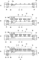
図1は、実施の形態1に係る半導体モジュールの構成を示す断面図である。半導体モジュール10は、素子搭載用基板20および半導体素子30を備える。半導体素子30は、素子電極(外部電極端子)が形成された電極形成面をフェイスダウンした状態で素子搭載用基板20に実装され、当該素子電極と、素子搭載用基板20に設けられた電極端子とがはんだを用いて電気的に接続されている。すなわち、半導体素子30は素子搭載用基板20にフリップチップ接続されている。
図1は、実施の形態1に係る半導体モジュールの構成を示す断面図である。半導体モジュール10は、素子搭載用基板20および半導体素子30を備える。半導体素子30は、素子電極(外部電極端子)が形成された電極形成面をフェイスダウンした状態で素子搭載用基板20に実装され、当該素子電極と、素子搭載用基板20に設けられた電極端子とがはんだを用いて電気的に接続されている。すなわち、半導体素子30は素子搭載用基板20にフリップチップ接続されている。
素子搭載用基板20は、絶縁樹脂層22と、絶縁樹脂層22の一方の主表面(半導体素子搭載側)に設けられた配線層24、保護層28と、絶縁樹脂層22の他方の主表面に設けられた配線層26、保護層28、はんだボール80を備える。
絶縁樹脂層22を構成する材料としては、たとえば、BTレジン等のメラミン誘導体、液晶ポリマー、エポキシ樹脂、PPE樹脂、ポリイミド樹脂、フッ素樹脂、フェノール樹脂、ポリアミドビスマレイミド等の熱硬化性樹脂が例示される。半導体モジュール10の放熱性向上の観点から、絶縁樹脂層22は高熱伝導性を有することが望ましい。このため、絶縁樹脂層22は、銀、ビスマス、銅、アルミニウム、マグネシウム、錫、亜鉛およびこれらの合金などを高熱伝導性フィラーとして含有することが好ましい。
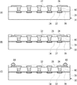
配線層24は、所定パターンを有し、絶縁樹脂層22の一方の主表面に設けられている。配線層24は、銅などの導電材料により形成される。配線層24は、半導体素子30を接続するための基板電極24a(電極パッド)を含む。基板電極24aは、本発明の「第1の電極」に相当する。基板電極24aの形状については後述する。
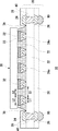
図2は、基板電極24aを含む配線層24のパターンの一例を示す平面図である。基板電極24aは、配線層24の一部から突出した櫛状をなしており(櫛状電極)、一対の櫛状電極が互いに対向し、一方の櫛状電極の櫛歯状部と他方の櫛状電極の櫛歯状部が互い違いに併設した構造を有する。フリップチップ接続用のはんだは、基板電極24aの上に形成される。なお、図2のA−A’線は、隣接する基板電極24aを最短距離で結ぶ線に相当し、図1は図2のA−A’線に沿った断面図に相当する。
図1に戻り、保護層28は、基板電極24aを除く配線層24を覆うように絶縁樹脂層22の一方の主表面に設けられている。保護層28によって配線層24の酸化や絶縁樹脂層22の劣化が抑制される。保護層28は、たとえばフォトソルダーレジストにより形成され、保護層28の厚さは、例えば10〜50μmである。
配線層26は、所定パターンを有し、絶縁樹脂層22の他方の主表面に設けられている。配線層26は、銅などの導電材料により形成される。配線層24および配線層26の厚さは、例えば10〜25μmである。
絶縁樹脂層22の所定位置において、絶縁樹脂層22を貫通するビア導体40が設けられている。ビア導体40は、例えば、銅めっきにより形成される。ビア導体40により、配線層24と配線層26とが電気的に接続されている。
保護層28は、配線層26を覆うように絶縁樹脂層22の他方の主表面にも設けられており、保護層28によって配線層26の酸化や絶縁樹脂層22の劣化が抑制される。保護層28には、配線層26の所定領域(ランド領域)上にはんだボール80を搭載するための開口部が設けられている。はんだボール80は、保護層28に設けられた開口部内において、配線層26に接続され、半導体モジュール10は、はんだボール80によって図示しないプリント配線基板に接続される。
半導体素子30は、IC(集積回路)、LSI(大規模集積回路)などの能動素子である。半導体素子30の電極形成面には、素子搭載用基板20に設けられた基板電極24aに対応して素子電極32(電極パッド)が設けられており、素子電極32の表面に銅ポスト33が形成されている。銅ポスト33の断面形状は素子電極32と同様である。この銅ポスト33と基板電極24aとがはんだ70により接続されている。素子電極32および銅ポスト33は、本発明の「第2の電極」に相当する。なお、銅ポスト33を介さずに、素子電極32と基板電極24aとがはんだ70により接続されていてもよい。この場合には、素子電極32が本発明の「第2の電極」に相当する。また、はんだ70は、本発明の「導電性接続部材」に相当する。
半導体素子30と素子搭載用基板20との間にアンダーフィル72が充填されている。アンダーフィル72により、基板電極24aと素子電極32とのはんだ接合部分が保護されるとともに、半導体素子30と素子搭載用基板20との間に働く応力が緩和されるため、半導体モジュール10の接続信頼性がより向上する。
ここで、基板電極24aの特徴について説明する。
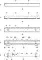
隣接する基板電極24aを結ぶ線に沿った断面において、基板電極24aの幅L1は、基板電極24aに対応する素子電極32の幅L2に比べて狭くなっている。より好ましくは、隣接する基板電極24aの間隔をS1、隣接する素子電極32の間隔をS2としたとき、基板電極24aのL/S比(L1/S1)は、素子電極32のL/S(L2/S2)より小さい。
この他、基板電極24aの側面は、基板電極24aの内側に傾いている。言い換えると、素子搭載用基板20の基板面と基板電極24aの側面とのなす角は鋭角である。この条件を満たせば、基板電極24aの形状は特に限定されないが、たとえば、隣接する基板電極24aを結ぶ線に沿った断面における基板電極24aの形状は略三角形状、台形状である。
以上の構成によれば、はんだ70が横方向(素子搭載用基板20の面方向)に広がることが抑制されるため、はんだ70が素子電極32の幅L2の内側に収まる。これにより、隣接する基板電極24aおよび素子電極32の間で短絡が生じることが抑制されるため、はんだ接続時の接続信頼性を損なうことなく、基板電極24aおよび素子電極32の狭ピッチ化を図ることができる。
また、はんだ70が横方向に広がることが抑制されることにより、素子搭載用基板20と半導体素子30との間にアンダーフィル72を充填する場合に、はんだ70がアンダーフィル72の充填の障害になることが低減し、素子搭載用基板20と半導体素子30との隙間にアンダーフィル72が入り込みやすくなる。この結果、アンダーフィル充填時にボイドが発生することが抑制される。
(実施の形態1の半導体モジュールの製造方法)
実施の形態1に係る素子搭載用基板および半導体モジュールの製造方法について図3および図4を参照して説明する。
実施の形態1に係る素子搭載用基板および半導体モジュールの製造方法について図3および図4を参照して説明する。
まず、図3(A)に示すように、一方の主表面に銅箔23が、他方の主表面に銅箔25が貼り付けられた絶縁樹脂層22を準備する。
次に、図3(B)に示すように、ドリル加工、レーザ加工などの掘削加工により、絶縁樹脂層22および銅箔23、25の所定領域にビアホール27を形成する。
次に、図3(C)に示すように、無電解めっき法および電解めっき法により、ビアホール27に銅を充填してビア導体40を形成するとともに、絶縁樹脂層22の主表面に設けられた銅箔23、25を厚膜化する。
そして、図3(D)に示すように、銅箔23、25の上にそれぞれ配線層24、24a、26に対応したレジストパターン100a、100b、102を形成する。
次に、図3(E)に示すように、レジストパターン100a、100bをマスクとしてウェットエッチングを行うことにより、絶縁樹脂層22の一方の主表面に基板電極24aを含む所定パターンの配線層24を形成する。ここで、隣接する基板電極24aを結ぶ線に沿った断面において、基板電極24aの幅L1が当該基板電極24aに対応する素子電極の幅よりも狭くなるようにパターニングを行う。より好ましくは、隣接する基板電極24aを結ぶ線に沿った断面において、基板電極24aの幅L1と隣接する基板電極24aの間隔S1との比(L1/S1)が、基板電極24aに対応する素子電極の幅L2と隣接する素子電極の間隔S2との比(L2/S2)より小さくなるようにパターニングを行う。また、基板電極24aの側面が基板電極24aの形成領域の内側に傾くようにパターニングを行う。
一方、レジストパターン102をマスクとしてウェットエッチングを行うことにより、絶縁樹脂層22の他方の主表面に配線層26を形成する。
次に、図4(A)に示すように、フォトソルダーレジストを積層した後、周知のフォトリソグラフィ法を用いて、絶縁樹脂層22の一方の主表面に基板電極24aを除く配線層24を被覆する保護層28を形成する。また、絶縁樹脂層22の他方の主表面において、所定領域に配線層26のランド領域が露出するような開口部を有する保護層28を形成する。
次に、図4(B)に示すように、電極形成面に素子電極32および銅ポスト33が設けられ、銅ポスト33にはんだ70が搭載された半導体素子30を準備する。そして、半導体素子30を素子搭載用基板20の上に搭載する。銅ポスト33は、たとえば、めっき法を用いて形成することができる。
次に、図4(C)に示すように、素子搭載用基板20に半導体素子30が搭載された状態で、リフロー工程により対応する銅ポスト33と基板電極24aとをはんだ70を用いて接合し、銅ポスト33と基板電極24aとを電気的に接続する。
次に、図4(D)に示すように、半導体素子30と素子搭載用基板20との間にアンダーフィル72を充填する。また、保護層28に設けられた開口部において、配線層26にはんだボール80を搭載する。
以上の工程により、実施の形態1に係る半導体モジュール10を製造することができる。なお、図示は省略するが、トランスファーモールド法などを用いて、半導体素子30を覆うように封止樹脂層により封止してもよい。
(実施の形態2)
図5は、実施の形態2に係る半導体モジュールの構成を示す断面図である。
図5は、実施の形態2に係る半導体モジュールの構成を示す断面図である。
半導体モジュール10は、素子搭載用基板20および半導体素子30を備える。
半導体素子30は、たとえば、P型シリコンウエハを用いて形成される。実装面となる主表面MS1に集積回路に接続された素子電極32が設けられている。素子電極32の材料として、アルミニウム(Al)や銅(Cu)などの金属が用いられる。素子電極32は、本発明の「第2の電極」に相当する。
素子電極32が露出するように半導体素子30の主表面MS1上に保護層34が形成されている。保護層34として、シリコン酸化膜(SiO2)やシリコン窒化膜(SiN)やポリイミド(PI)膜などが好適である。
素子搭載用基板20は、絶縁樹脂層22と、絶縁樹脂層22の半導体素子30と反対側の主表面に設けられた配線層24(再配線)と、配線層24と一体的に形成され、配線層24から絶縁樹脂層22側に突出している突起電極90とを備える。突起電極90は、本発明の「第1の電極」に相当する。なお、図5は、隣接する突起電極90を最短距離で結ぶ線に沿った断面図に相当する。
絶縁樹脂層22は、絶縁性の樹脂からなり、たとえば加熱または加圧したときに塑性流動を引き起こす材料で形成されている。加圧したときに塑性流動を引き起こす材料としては、エポキシ系熱硬化型樹脂が挙げられる。絶縁樹脂層22に用いられるエポキシ系熱硬化型樹脂は、たとえば、温度160℃、圧力8Mpaの条件下で、粘度が1kPa・sの特性を有する材料であればよい。また、このエポキシ系熱硬化型樹脂は、たとえば温度160℃の条件下で、5〜15Mpaで加圧した場合に、加圧しない場合と比較して、樹脂の粘度が約1/8に低下する。これに対して、熱硬化前のBステージのエポキシ樹脂は、ガラス転移温度Tg以下の条件下では、樹脂を加圧しない場合と同程度に、粘性がなく、加圧しても粘性は生じない。また、このエポキシ系熱硬化型樹脂は、約3〜4の誘電率を有する誘電体である。
配線層24は、絶縁樹脂層22の半導体素子30と反対側の主表面に設けられており、導電材料、好ましくは圧延金属、さらには圧延銅により形成される。圧延銅は、めっき処理等によって形成された銅からなる金属膜と比較すると、機械的強度の点において強いので、再配線のための材料として優れている。なお、配線層24は電解銅などで形成されてもよい。本実施の形態においては、配線層24と突起電極90とは一体的に形成されており、それにより配線層24と突起電極90との接続が確実になっている。
突起電極90はその全体的な形状が、先端に近づくにつれて径が細くなっている。言い換えると、突起電極90の側面は電極形成領域の内側に傾いたテーパ状となっている。言い換えると、配線層24の面と突起電極90の側面とのなす角は鋭角である。突起電極90の先端(頂部面)の径および基面の径は、それぞれたとえば約45μmφおよび約60μmφである。また、突起電極90の高さは、たとえば、20μmである。突起電極90の頂部面と突起電極90に対応する素子電極32とは、はんだ70により接合されている。
隣接する突起電極90を結ぶ線に沿った断面において、突起電極90の基底部の幅L1は、突起電極90に対応する素子電極32の幅L2に比べて狭くなっている。より好ましくは、隣接する突起電極90の基底部の間隔をS1、隣接する素子電極32の間隔をS2としたとき、突起電極90のL/S比(L1/S1)は、素子電極32のL/S(L2/S2)より小さい。さらに、突起電極90の形状は、先端に近づくにつれて径が細くなっているため、突起電極90の頂部面の幅L1’は突起電極90の基底部の幅L1より狭い。
配線層24の絶縁樹脂層22と反対側の主表面には、配線層24の酸化などを防ぐための保護層28が設けられている。保護層28としては、ソルダーレジスト層などが挙げられる。保護層28の所定の領域には開口部が形成されており、開口部によって配線層24の一部が露出している。開口部内には外部接続電極としてのはんだボール80が形成され、はんだボール80と配線層24とが電気的に接続されている。はんだボール80を形成する位置、すなわち開口部の形成領域は、たとえば再配線(配線層24)で引き回した先の端部である。
(実施の形態2の半導体モジュールの製造方法)
実施の形態2に係る素子搭載用基板および半導体モジュールの製造方法について図6乃至図10を参照して説明する。
実施の形態2に係る素子搭載用基板および半導体モジュールの製造方法について図6乃至図10を参照して説明する。
まず、図6(A)に示すように、あらかじめ半導体基板31の一方の主表面に素子電極32および保護層34が形成された半導体素子30を用意する。具体的には、P型シリコン基板などの半導体基板31に対して、周知のリソグラフィ技術、エッチング技術、イオン注入技術、成膜技術、及び熱処理技術などを組み合わせた半導体製造プロセスを用いて一方の主表面に所定の集積回路とその外周縁部に素子電極32を形成する。素子電極32の材料にはアルミニウムや銅などの金属が採用される。これらの素子電極32を除いた半導体基板31の主表面上に、半導体基板31を保護するための絶縁性の保護層34が形成されている。保護層34としてはシリコン酸化膜(SiO2)やシリコン窒化膜(SiN)やポリイミド(PI)などが採用される。
次に、図6(B)に示すように、保護層34の開口部において露出する素子電極32の上にスクリーン印刷法によりはんだ70を搭載する。具体的には、樹脂とはんだ材をペースト状にしたはんだペーストをスクリーンマスクにより所望の箇所に印刷し、はんだ溶融温度に加熱することではんだ70を形成する。
一方、図7(A)に示すように、図5に示したような突起電極90の高さと配線層24の厚さとの和より少なくとも大きい厚さを有する金属板としての銅板200を用意する。銅板200の厚さは、たとえば125μmである。銅板200としては圧延された銅からなる圧延金属が採用される。
次に、図7(B)に示すように、リソグラフィ法により、突起電極の形成予定領域に対応したパターンに合わせてレジスト210を選択的に形成する。具体的には、ラミネーター装置を用いて銅板200に所定膜厚のレジスト膜を貼り付け、突起電極90のパターンを有するフォトマスクを用いて露光した後、現像することによって、銅板200の上にレジスト210が選択的に形成される。なお、レジストとの密着性向上のために、レジスト膜のラミネート前に、銅板200の表面に研磨、洗浄等の前処理を必要に応じて施すことが望ましい。なお、レジスト210を設けた面と反対側(上面側)の全面にはレジスト保護膜(図示せず)を形成して銅板200を保護しておくことが望ましい。
次に、図7(C)に示すように、レジスト210をマスクとして塩化第二鉄溶液などの薬液を用いたウェットエッチング処理を行うことにより、銅板200の表面から突出する所定の円錐台パターンの突起電極90を形成する。この際、突起電極90はその先端部に近づくにつれて径(寸法)が細くなるテーパ状の側面部を有するように形成される。当該ウェットエッチング処理は、突起電極90の基底部の径(幅)L1が、突起電極90に対応する素子電極32の幅L2(図1参照)よりも狭くなるような条件で行われる。本実施形態の突起電極90における基底部の径、頂部の径、高さは、たとえばそれぞれ、100〜140μmφ、50μmφ、20〜25μmである。
次に、図7(D)に示すように、レジスト210およびレジスト保護膜を剥離剤を用いて剥離する。以上説明した工程により、銅板200に突起電極90が一体的に形成される。なお、レジスト210に代えて銀(Ag)などの金属マスクを採用してもよい。この場合には銅板200とのエッチング選択比が十分確保されるため、突起電極90のパターニングのさらなる微細化を図ることが可能となる。
次に、図8(A)に示すように、真空ラミネート法を用いて、突起電極90が設けられた側の銅板200の表面に絶縁樹脂層22を積層する。絶縁樹脂層22としては、上述したように、加圧または加熱により可塑性または変形を引き起こす絶縁材料が用いられる。
次に、図8(B)に示すように、O2プラズマエッチングを用いて、突起電極90の頂部面が露出するように絶縁樹脂層22を薄膜化する。
次に、図8(C)に示すように、塩化第二鉄溶液などの薬液を用いたウェットエッチング処理などにより、突起電極90が設けられた側と反対側の銅板200の表面をエッチバックし銅板200を薄膜化する。この際、突起電極90が設けられた側にはレジスト保護膜(図示せず)を形成して突起電極90および銅板200を保護しておき、エッチング処理後にレジスト保護膜を除去する。これにより、所定の厚さ(配線層24の厚さ)に加工され、所定の突起電極90が一体的に設けられた銅板200が形成される。本実施形態の銅板200の厚さは約20μmである。
次に、図9(A)に示すように、プレス機を構成する一対の平板プレート500a、500bの間に、半導体素子30と、突起電極90が一体的に形成された銅板200とを設置する。この際に、対応する突起電極90と素子電極32との位置合わせを行う。
次に、図9(B)に示すように、プレス機を用いて加圧成形することにより、対応する突起電極90と素子電極32とが当接した状態で半導体素子30と銅板200とを圧着する。プレス加工時の圧力および温度は、それぞれ約17kNおよび200℃である。この工程の際、またはこの工程の後、リフローによりはんだ70を溶融し、はんだ70により対応する突起電極90と素子電極32とを接合する。溶融したはんだ70と突起電極90の頂部面との濡れ性は、溶融したはんだ70と絶縁樹脂層22との濡れ性に比べて高いため、はんだ70は突起電極90の頂部面に引き寄せられ、突起電極90の頂部面近傍において、はんだ70の幅は突起電極90の頂部面内に収まる。
次に、図10(A)に示すように、リソグラフィ技術およびエッチング技術を用いて銅板200を所定の配線パターンに加工することにより、配線層24(再配線)を形成する。
次に、図10(B)に示すように、配線層24および絶縁樹脂層22の上に保護層(フォトソルダーレジスト層)28を積層した後、フォトリソグラフィ法により保護層28の所定領域(はんだボール搭載領域)に開口部を設ける。保護層28は配線層24の保護膜として機能する。保護層28にはエポキシ樹脂などが採用され、その膜厚は、たとえば、約40μmである。
次に、図10(C)に示すように、保護層28の開口部にスクリーン印刷法によりはんだボール80を搭載する。具体的には、樹脂とはんだ材をペースト状にしたはんだペーストをスクリーンマスクにより所望の箇所に印刷し、はんだ溶融温度に加熱することではんだボール80を形成する。
以上の工程により実施の形態2に係る半導体モジュールを製造することができる。
以上説明した半導体モジュール10によれば、突起電極90の頂部面近傍において、はんだ70は突起電極90の頂部面の幅L1’に収まる。突起電極90の頂部面の幅L1’は、突起電極90の基底部の幅L1より狭く、かつ、突起電極90の基底部の幅L1は、突起電極90に対応する素子電極32の幅L2に比べて狭い。すなわち、はんだ70の突起電極90側における幅は素子電極32の幅L2の内側に収まるように、横方向(素子搭載用基板20の面方向)に広がることが抑制される。これにより、隣接する基板電極24aおよび素子電極32の間で短絡が生じることが抑制されるため、はんだ接続時の接続信頼性を損なうことなく、基板電極24aおよび素子電極32の狭ピッチ化を図ることができる。
なお、本実施の形態では、はんだ70は突起電極90の頂部面と素子電極32との間に設けられており、はんだ70は突起電極90の頂部面に接しているが、素子電極32の幅L2の内側に収まっていれば、突起電極90の側面に接していてもよい。
具体的には、図11に示す変形例のように、突起電極90の先端部分の側面部分と絶縁樹脂層22との間に隙間が生じており、この隙間にはんだ70が入り込むことにより、突起電極90の先端部の側面にはんだ70が接していてもよい。この場合においても、突起電極90の側面部分の幅は、突起電極90の基底部の幅L1より狭く、突起電極90と接するはんだ70の幅は、突起電極90の基底部の幅L1より狭くなる。すなわち、はんだ70の突起電極90側における幅は素子電極32の幅L2の内側に収まるように、横方向(素子搭載用基板20の面方向)に広がることが抑制される。
(携帯機器への適用)
次に、本発明の半導体モジュールを備えた携帯機器について説明する。なお、携帯機器として携帯電話に搭載する例を示すが、たとえば、個人用携帯情報端末(PDA)、デジタルビデオカメラ(DVC)、音楽プレーヤ、及びデジタルスチルカメラ(DSC)といった電子機器であってもよい。
次に、本発明の半導体モジュールを備えた携帯機器について説明する。なお、携帯機器として携帯電話に搭載する例を示すが、たとえば、個人用携帯情報端末(PDA)、デジタルビデオカメラ(DVC)、音楽プレーヤ、及びデジタルスチルカメラ(DSC)といった電子機器であってもよい。
図12は実施の形態に係る半導体モジュール10を備えた携帯電話の構成を示す図である。携帯電話1111は、第1の筐体1112と第2の筐体1114が可動部1120によって連結される構造になっている。第1の筐体1112と第2の筐体1114は可動部1120を軸として回動可能である。第1の筐体1112には文字や画像等の情報を表示する表示部1118やスピーカ部1124が設けられている。第2の筐体1114には操作用ボタンなどの操作部1122やマイク部1126が設けられている。なお、本発明の各実施形態に係る半導体モジュールのいずれかがこうした携帯電話1111の内部に搭載されている。なお、このように、携帯電話に搭載した本発明の半導体モジュールとしては、各回路を駆動するための電源回路、RF発生するRF発生回路、DAC、エンコーダ回路、携帯電話の表示部に採用される液晶パネルの光源としてのバックライトの駆動回路などとして採用することが可能である。
図13は図12に示した携帯電話の部分断面図(第1の筐体1112の断面図)である。本発明の実施形態に係る半導体モジュール10は、はんだボール80を介してプリント基板1128に搭載され、こうしたプリント基板1128を介して表示部1118などと電気的に接続されている。また、半導体モジュール10の裏面側(はんだボール80とは反対側の面)には金属基板などの放熱基板1116が設けられ、たとえば、半導体モジュール10から発生する熱を第1の筐体1112内部に篭もらせることなく、効率的に第1の筐体1112の外部に放熱することができるようになっている。
本発明の実施形態に係る半導体モジュールを備えた携帯機器によれば、以下の効果を得ることができる。
半導体モジュール10において、基板側の第1の電極と半導体素子側の第2の電極との接続信頼性が向上した結果、半導体モジュール10の動作信頼性が向上するので、こうした半導体モジュール10を搭載した携帯機器の動作信頼性が向上する。
放熱基板1116を介して半導体モジュール10からの熱を効率的に外部に放熱することができるので、半導体モジュール10の温度上昇が抑制され、導電性部材と配線層との間の熱応力が低減される。このため、放熱基板1116を設けない場合に比べ、半導体モジュール内の導電性部材が配線層から剥離することが防止され、半導体モジュール10の信頼性(耐熱信頼性)が向上する。この結果、携帯機器の信頼性(耐熱信頼性)を向上させることができる。
上記実施の形態で示した半導体モジュール10は小型化が可能であるので、こうした半導体モジュール10を搭載した携帯機器の薄型化・小型化を図ることができる。
本発明は、上述の各実施の形態に限定されるものではなく、当業者の知識に基づいて各種の設計変更等の変形を加えることも可能であり、そのような変形が加えられた実施の形態も本発明の範囲に含まれうるものである。
たとえば、上述の各実施の形態では、素子搭載用基板20に設けられた電極と、半導体素子30に設けられた電極とを電気的に接続する導電性接続部材として、はんだが用いられているが、導電性接続部材としては、はんだ以外に、銀ペーストなどの導電性ペーストを用いてもよい。
10 半導体モジュール、20 素子搭載用基板、22 絶縁樹脂層、24、26 配線層
Claims (7)
- 第1の電極が設けられた基板と、
第2の電極が設けられた半導体素子と、
前記第1の電極と前記第2の電極とを接続する導電性接続部材と、
を備え、
隣接する前記第1の電極を最短距離で結ぶ線に沿った断面において、前記第1の電極の幅が、前記第1の電極に対応する前記第2の電極の幅に比べて狭いことを特徴とする半導体モジュール。 - 隣接する前記第1の電極を最短距離で結ぶ線に沿った断面において、前記第1の電極の幅L1と隣接する前記第1の電極の間隔S1との比(L1/S1)が、前記第1の電極に対応する前記第2の電極の幅L2と隣接する前記第2の電極の間隔S2との比(L2/S2)より小さい請求項1に記載の半導体モジュール。
- 隣接する前記第1の電極を最短距離で結ぶ線に沿った断面において、前記第1の電極の側面が電極形成領域の内側に傾いている請求項1または2に記載の半導体モジュール。
- 前記第1の電極が前記基板に設けられた配線層から前記半導体素子の側へ突出する突起電極である請求項1乃至3のいずれか1項に記載の半導体モジュール。
- 隣接する前記第1の電極を最短距離で結ぶ線に沿った断面において、前記第1の電極の形状が略三角形または台形である請求項1乃至4のいずれか1項に記載の半導体モジュール。
- 請求項1乃至5のいずれか1項に記載の半導体モジュールを備えることを特徴とする携帯機器。
- 基板の一方の主表面に、隣接する基板電極を含む配線層をパターニングする配線形成工程と、
前記基板電極に対応して半導体素子に設けられた素子電極と前記基板電極とを導電性接続部材を用いて接続し、前記基板に前記半導体素子を搭載する素子搭載工程と、
を備え、
配線形成工程において、隣接する前記基板電極を最短距離で結ぶ線に沿った断面において、前記基板電極の幅が前記基板電極に対応する前記素子電極の幅よりも狭くなるように前記基板電極を形成することを特徴とする半導体モジュールの製造方法。
Priority Applications (3)
| Application Number | Priority Date | Filing Date | Title |
|---|---|---|---|
| JP2008314960A JP2010141055A (ja) | 2008-12-10 | 2008-12-10 | 半導体モジュール、半導体モジュールの製造方法および携帯機器 |
| US13/139,075 US20110241203A1 (en) | 2008-12-10 | 2009-12-10 | Semiconductor module, method for manufacturing semiconductor module, and portable apparatus |
| PCT/JP2009/006765 WO2010067610A1 (ja) | 2008-12-10 | 2009-12-10 | 半導体モジュール、半導体モジュールの製造方法および携帯機器 |
Applications Claiming Priority (1)
| Application Number | Priority Date | Filing Date | Title |
|---|---|---|---|
| JP2008314960A JP2010141055A (ja) | 2008-12-10 | 2008-12-10 | 半導体モジュール、半導体モジュールの製造方法および携帯機器 |
Publications (1)
| Publication Number | Publication Date |
|---|---|
| JP2010141055A true JP2010141055A (ja) | 2010-06-24 |
Family
ID=42242602
Family Applications (1)
| Application Number | Title | Priority Date | Filing Date |
|---|---|---|---|
| JP2008314960A Withdrawn JP2010141055A (ja) | 2008-12-10 | 2008-12-10 | 半導体モジュール、半導体モジュールの製造方法および携帯機器 |
Country Status (3)
| Country | Link |
|---|---|
| US (1) | US20110241203A1 (ja) |
| JP (1) | JP2010141055A (ja) |
| WO (1) | WO2010067610A1 (ja) |
Cited By (6)
| Publication number | Priority date | Publication date | Assignee | Title |
|---|---|---|---|---|
| CN102468197A (zh) * | 2010-11-16 | 2012-05-23 | 新科金朋有限公司 | 半导体器件以及形成倒装芯片互连结构的方法 |
| CN102487021A (zh) * | 2010-12-03 | 2012-06-06 | 新科金朋有限公司 | 形成用于倒装半导体管芯的焊盘布局的半导体器件和方法 |
| KR20120067266A (ko) * | 2010-12-15 | 2012-06-25 | 스태츠 칩팩, 엘티디. | 반도체 소자 및 그 제조 방법 |
| JP2016178247A (ja) * | 2015-03-20 | 2016-10-06 | 新光電気工業株式会社 | 配線基板、半導体装置及び配線基板の製造方法 |
| KR101794353B1 (ko) * | 2010-12-06 | 2017-11-06 | 스태츠 칩팩 피티이. 엘티디. | 반도체 소자 및 그 제조 방법 |
| KR101807311B1 (ko) * | 2010-12-03 | 2017-12-08 | 스태츠 칩팩 피티이. 엘티디. | 반도체 소자 및 그 제조 방법 |
Families Citing this family (15)
| Publication number | Priority date | Publication date | Assignee | Title |
|---|---|---|---|---|
| US9029196B2 (en) | 2003-11-10 | 2015-05-12 | Stats Chippac, Ltd. | Semiconductor device and method of self-confinement of conductive bump material during reflow without solder mask |
| US8026128B2 (en) | 2004-11-10 | 2011-09-27 | Stats Chippac, Ltd. | Semiconductor device and method of self-confinement of conductive bump material during reflow without solder mask |
| TWI478254B (zh) | 2003-11-10 | 2015-03-21 | 恰巴克有限公司 | 引線上凸塊之倒裝晶片互連 |
| US9659893B2 (en) | 2011-12-21 | 2017-05-23 | Mediatek Inc. | Semiconductor package |
| US8633588B2 (en) | 2011-12-21 | 2014-01-21 | Mediatek Inc. | Semiconductor package |
| US9461008B2 (en) * | 2012-08-16 | 2016-10-04 | Qualcomm Incorporated | Solder on trace technology for interconnect attachment |
| KR20140086531A (ko) * | 2012-12-28 | 2014-07-08 | 삼성전기주식회사 | 패키지 기판 및 그 제조방법, 그리고 패키지 온 패키지 기판 |
| US9159670B2 (en) | 2013-08-29 | 2015-10-13 | Qualcomm Incorporated | Ultra fine pitch and spacing interconnects for substrate |
| US9806046B2 (en) * | 2014-03-13 | 2017-10-31 | Taiwan Semiconductor Manufacturing Co., Ltd | Semiconductor device structure and manufacturing method |
| TWI538127B (zh) * | 2014-03-28 | 2016-06-11 | 恆勁科技股份有限公司 | 封裝裝置及其製作方法 |
| TWI624018B (zh) * | 2014-08-04 | 2018-05-11 | 恆勁科技股份有限公司 | 封裝結構及其製法 |
| JP2015201661A (ja) * | 2015-06-19 | 2015-11-12 | ルネサスエレクトロニクス株式会社 | 半導体装置 |
| US11189555B2 (en) * | 2019-01-30 | 2021-11-30 | Delta Electronics, Inc. | Chip packaging with multilayer conductive circuit |
| KR102732191B1 (ko) * | 2019-08-09 | 2024-11-19 | 나가세케무텍쿠스가부시키가이샤 | 몰드 언더필 봉지용의 다층 시트, 몰드 언더필 봉지 방법, 전자 부품 실장 기판 및 전자 부품 실장 기판의 제조 방법 |
| CN111554641A (zh) * | 2020-05-11 | 2020-08-18 | 上海天马微电子有限公司 | 半导体封装件及其制作方法 |
Family Cites Families (3)
| Publication number | Priority date | Publication date | Assignee | Title |
|---|---|---|---|---|
| JPS57143838A (en) * | 1981-02-27 | 1982-09-06 | Mitsubishi Electric Corp | Manufacture of semiconductor device |
| US20060286716A1 (en) * | 2002-12-18 | 2006-12-21 | K-Tec Devices Corp. | Flip-chip mounting electronic component and method for producing the same, circuit board and method for producing the same, method for producing package |
| US8115310B2 (en) * | 2009-06-11 | 2012-02-14 | Texas Instruments Incorporated | Copper pillar bonding for fine pitch flip chip devices |
-
2008
- 2008-12-10 JP JP2008314960A patent/JP2010141055A/ja not_active Withdrawn
-
2009
- 2009-12-10 WO PCT/JP2009/006765 patent/WO2010067610A1/ja not_active Ceased
- 2009-12-10 US US13/139,075 patent/US20110241203A1/en not_active Abandoned
Cited By (10)
| Publication number | Priority date | Publication date | Assignee | Title |
|---|---|---|---|---|
| CN102468197A (zh) * | 2010-11-16 | 2012-05-23 | 新科金朋有限公司 | 半导体器件以及形成倒装芯片互连结构的方法 |
| KR101785729B1 (ko) * | 2010-11-16 | 2017-11-06 | 스태츠 칩팩 피티이. 엘티디. | 반도체 소자 및 그 제조 방법 |
| CN102487021A (zh) * | 2010-12-03 | 2012-06-06 | 新科金朋有限公司 | 形成用于倒装半导体管芯的焊盘布局的半导体器件和方法 |
| KR101798657B1 (ko) * | 2010-12-03 | 2017-11-16 | 스태츠 칩팩 피티이. 엘티디. | 반도체 소자 및 그 제조 방법 |
| KR101807311B1 (ko) * | 2010-12-03 | 2017-12-08 | 스태츠 칩팩 피티이. 엘티디. | 반도체 소자 및 그 제조 방법 |
| TWI667759B (zh) * | 2010-12-03 | 2019-08-01 | 新加坡商史達晶片有限公司 | 形成用於覆晶半導體晶粒的墊佈局的半導體裝置及方法 |
| KR101794353B1 (ko) * | 2010-12-06 | 2017-11-06 | 스태츠 칩팩 피티이. 엘티디. | 반도체 소자 및 그 제조 방법 |
| KR20120067266A (ko) * | 2010-12-15 | 2012-06-25 | 스태츠 칩팩, 엘티디. | 반도체 소자 및 그 제조 방법 |
| KR101979024B1 (ko) * | 2010-12-15 | 2019-08-28 | 스태츠 칩팩 피티이. 엘티디. | 반도체 소자 및 그 제조 방법 |
| JP2016178247A (ja) * | 2015-03-20 | 2016-10-06 | 新光電気工業株式会社 | 配線基板、半導体装置及び配線基板の製造方法 |
Also Published As
| Publication number | Publication date |
|---|---|
| US20110241203A1 (en) | 2011-10-06 |
| WO2010067610A1 (ja) | 2010-06-17 |
Similar Documents
| Publication | Publication Date | Title |
|---|---|---|
| JP2010141055A (ja) | 半導体モジュール、半導体モジュールの製造方法および携帯機器 | |
| JP5091600B2 (ja) | 半導体モジュール、半導体モジュールの製造方法および携帯機器 | |
| JP4498404B2 (ja) | 素子搭載用基板およびその製造方法、半導体モジュールならびに携帯機器 | |
| CN102124563B (zh) | 元件搭载用基板、半导体模块、半导体装置、元件搭载用基板的制造方法、半导体装置的制造方法及便携式设备 | |
| US8274148B2 (en) | Semiconductor module | |
| US7989359B2 (en) | Semiconductor module manufacturing method, semiconductor module, and mobile device | |
| JP2009206506A (ja) | 素子搭載用基板およびその製造方法、半導体モジュールおよびこれを搭載した携帯機器 | |
| USRE50741E1 (en) | Semiconductor module and portable apparatus provided with semiconductor module | |
| WO2009144960A1 (ja) | 半導体モジュール、半導体モジュールの製造方法および携帯機器 | |
| JP5135246B2 (ja) | 半導体モジュールおよびその製造方法、ならびに携帯機器 | |
| US20100078813A1 (en) | Semiconductor module and method for manufacturing the semiconductor module | |
| JP2008053693A (ja) | 半導体モジュール、携帯機器、および半導体モジュールの製造方法 | |
| JP2009224581A (ja) | 素子搭載用基板およびその製造方法、半導体モジュールおよびその製造方法、電極構造、携帯機器 | |
| JP2011054670A (ja) | 半導体モジュールおよびその製造方法、ならびに携帯機器 | |
| JP2013165087A (ja) | 半導体モジュールおよび半導体モジュールの製造方法 | |
| JP5484705B2 (ja) | 半導体モジュールおよび半導体モジュールを備える携帯機器 | |
| CN101510538A (zh) | 元件搭载用基板及其制造方法、半导体组件及便携式设备 | |
| JP2009158830A (ja) | 素子搭載用基板およびその製造方法、半導体モジュールおよびその製造方法、ならびに携帯機器 | |
| US20100140797A1 (en) | Device mounting board and method of manufacturing the board, semiconductor module and method of manufacturing the module | |
| JP2008218521A (ja) | 回路装置およびその製造方法 | |
| JP5295211B2 (ja) | 半導体モジュールの製造方法 | |
| JP2010040721A (ja) | 半導体モジュール、半導体装置、携帯機器、半導体モジュールの製造方法および半導体装置の製造方法 | |
| JP5002633B2 (ja) | 半導体モジュールおよび携帯機器 | |
| JP5022963B2 (ja) | 突起電極の構造、素子搭載用基板およびその製造方法、半導体モジュール、ならびに携帯機器 | |
| CN101494213A (zh) | 元件安装用基板、半导体组件及其制造方法及便携式设备 |
Legal Events
| Date | Code | Title | Description |
|---|---|---|---|
| A621 | Written request for application examination |
Free format text: JAPANESE INTERMEDIATE CODE: A621 Effective date: 20111130 |
|
| A761 | Written withdrawal of application |
Free format text: JAPANESE INTERMEDIATE CODE: A761 Effective date: 20130410 |