JP2010045369A - ピンホールアンダーカット部を含む装置と工程 - Google Patents
ピンホールアンダーカット部を含む装置と工程 Download PDFInfo
- Publication number
- JP2010045369A JP2010045369A JP2009187638A JP2009187638A JP2010045369A JP 2010045369 A JP2010045369 A JP 2010045369A JP 2009187638 A JP2009187638 A JP 2009187638A JP 2009187638 A JP2009187638 A JP 2009187638A JP 2010045369 A JP2010045369 A JP 2010045369A
- Authority
- JP
- Japan
- Prior art keywords
- region
- dielectric
- conductive region
- lower conductive
- undercut
- Prior art date
- Legal status (The legal status is an assumption and is not a legal conclusion. Google has not performed a legal analysis and makes no representation as to the accuracy of the status listed.)
- Pending
Links
- 238000000034 method Methods 0.000 title claims description 22
- 238000004519 manufacturing process Methods 0.000 claims abstract description 11
- 239000010409 thin film Substances 0.000 claims description 20
- 238000005530 etching Methods 0.000 claims description 13
- 230000000694 effects Effects 0.000 abstract description 4
- 230000002411 adverse Effects 0.000 abstract description 3
- 239000010410 layer Substances 0.000 description 38
- 239000004065 semiconductor Substances 0.000 description 37
- 239000000463 material Substances 0.000 description 15
- 239000000758 substrate Substances 0.000 description 15
- RYGMFSIKBFXOCR-UHFFFAOYSA-N Copper Chemical compound [Cu] RYGMFSIKBFXOCR-UHFFFAOYSA-N 0.000 description 10
- 229910052802 copper Inorganic materials 0.000 description 10
- 239000010949 copper Substances 0.000 description 10
- 229910052751 metal Inorganic materials 0.000 description 9
- 239000002184 metal Substances 0.000 description 9
- 239000003990 capacitor Substances 0.000 description 8
- 239000000203 mixture Substances 0.000 description 7
- LRHPLDYGYMQRHN-UHFFFAOYSA-N N-Butanol Chemical compound CCCCO LRHPLDYGYMQRHN-UHFFFAOYSA-N 0.000 description 6
- PCHJSUWPFVWCPO-UHFFFAOYSA-N gold Chemical compound [Au] PCHJSUWPFVWCPO-UHFFFAOYSA-N 0.000 description 6
- 229910052737 gold Inorganic materials 0.000 description 6
- 239000010931 gold Substances 0.000 description 6
- 239000000243 solution Substances 0.000 description 6
- 238000004528 spin coating Methods 0.000 description 6
- 230000000052 comparative effect Effects 0.000 description 5
- 238000000151 deposition Methods 0.000 description 5
- 239000003989 dielectric material Substances 0.000 description 5
- 239000011521 glass Substances 0.000 description 5
- 229920000123 polythiophene Polymers 0.000 description 5
- KFZMGEQAYNKOFK-UHFFFAOYSA-N Isopropanol Chemical compound CC(C)O KFZMGEQAYNKOFK-UHFFFAOYSA-N 0.000 description 4
- PXHVJJICTQNCMI-UHFFFAOYSA-N Nickel Chemical compound [Ni] PXHVJJICTQNCMI-UHFFFAOYSA-N 0.000 description 4
- BQCADISMDOOEFD-UHFFFAOYSA-N Silver Chemical compound [Ag] BQCADISMDOOEFD-UHFFFAOYSA-N 0.000 description 4
- 229920001940 conductive polymer Polymers 0.000 description 4
- 239000004020 conductor Substances 0.000 description 4
- 239000007772 electrode material Substances 0.000 description 4
- 239000010408 film Substances 0.000 description 4
- 239000000976 ink Substances 0.000 description 4
- 239000007788 liquid Substances 0.000 description 4
- BASFCYQUMIYNBI-UHFFFAOYSA-N platinum Chemical compound [Pt] BASFCYQUMIYNBI-UHFFFAOYSA-N 0.000 description 4
- 238000007639 printing Methods 0.000 description 4
- 239000002356 single layer Substances 0.000 description 4
- QTBSBXVTEAMEQO-UHFFFAOYSA-N Acetic acid Chemical compound CC(O)=O QTBSBXVTEAMEQO-UHFFFAOYSA-N 0.000 description 3
- 239000004642 Polyimide Substances 0.000 description 3
- XUIMIQQOPSSXEZ-UHFFFAOYSA-N Silicon Chemical compound [Si] XUIMIQQOPSSXEZ-UHFFFAOYSA-N 0.000 description 3
- HEMHJVSKTPXQMS-UHFFFAOYSA-M Sodium hydroxide Chemical compound [OH-].[Na+] HEMHJVSKTPXQMS-UHFFFAOYSA-M 0.000 description 3
- RTAQQCXQSZGOHL-UHFFFAOYSA-N Titanium Chemical compound [Ti] RTAQQCXQSZGOHL-UHFFFAOYSA-N 0.000 description 3
- 229910052782 aluminium Inorganic materials 0.000 description 3
- XAGFODPZIPBFFR-UHFFFAOYSA-N aluminium Chemical compound [Al] XAGFODPZIPBFFR-UHFFFAOYSA-N 0.000 description 3
- MWPLVEDNUUSJAV-UHFFFAOYSA-N anthracene Chemical class C1=CC=CC2=CC3=CC=CC=C3C=C21 MWPLVEDNUUSJAV-UHFFFAOYSA-N 0.000 description 3
- 239000011248 coating agent Substances 0.000 description 3
- 238000000576 coating method Methods 0.000 description 3
- 230000007547 defect Effects 0.000 description 3
- 150000002739 metals Chemical class 0.000 description 3
- 229920000515 polycarbonate Polymers 0.000 description 3
- 239000004417 polycarbonate Substances 0.000 description 3
- 229920000728 polyester Polymers 0.000 description 3
- 229920001721 polyimide Polymers 0.000 description 3
- 229920000642 polymer Polymers 0.000 description 3
- 239000011241 protective layer Substances 0.000 description 3
- 229910052710 silicon Inorganic materials 0.000 description 3
- 239000010703 silicon Substances 0.000 description 3
- 229910052709 silver Inorganic materials 0.000 description 3
- 239000004332 silver Substances 0.000 description 3
- JESXATFQYMPTNL-UHFFFAOYSA-N 2-ethenylphenol Chemical compound OC1=CC=CC=C1C=C JESXATFQYMPTNL-UHFFFAOYSA-N 0.000 description 2
- VYZAMTAEIAYCRO-UHFFFAOYSA-N Chromium Chemical compound [Cr] VYZAMTAEIAYCRO-UHFFFAOYSA-N 0.000 description 2
- 229920001609 Poly(3,4-ethylenedioxythiophene) Polymers 0.000 description 2
- 229910052581 Si3N4 Inorganic materials 0.000 description 2
- VYPSYNLAJGMNEJ-UHFFFAOYSA-N Silicium dioxide Chemical compound O=[Si]=O VYPSYNLAJGMNEJ-UHFFFAOYSA-N 0.000 description 2
- 230000015572 biosynthetic process Effects 0.000 description 2
- 229910052804 chromium Inorganic materials 0.000 description 2
- 239000011651 chromium Substances 0.000 description 2
- 238000004132 cross linking Methods 0.000 description 2
- 230000002950 deficient Effects 0.000 description 2
- 238000003618 dip coating Methods 0.000 description 2
- 239000012153 distilled water Substances 0.000 description 2
- 238000007647 flexography Methods 0.000 description 2
- 238000007654 immersion Methods 0.000 description 2
- 229910010272 inorganic material Inorganic materials 0.000 description 2
- 239000011147 inorganic material Substances 0.000 description 2
- 229910052759 nickel Inorganic materials 0.000 description 2
- 238000000206 photolithography Methods 0.000 description 2
- 239000002985 plastic film Substances 0.000 description 2
- 229910052697 platinum Inorganic materials 0.000 description 2
- 229920003217 poly(methylsilsesquioxane) Polymers 0.000 description 2
- KWYUFKZDYYNOTN-UHFFFAOYSA-M potassium hydroxide Inorganic materials [OH-].[K+] KWYUFKZDYYNOTN-UHFFFAOYSA-M 0.000 description 2
- HQVNEWCFYHHQES-UHFFFAOYSA-N silicon nitride Chemical compound N12[Si]34N5[Si]62N3[Si]51N64 HQVNEWCFYHHQES-UHFFFAOYSA-N 0.000 description 2
- 229910052814 silicon oxide Inorganic materials 0.000 description 2
- 239000010936 titanium Substances 0.000 description 2
- 229910052719 titanium Inorganic materials 0.000 description 2
- 238000001771 vacuum deposition Methods 0.000 description 2
- XLYOFNOQVPJJNP-UHFFFAOYSA-N water Chemical compound O XLYOFNOQVPJJNP-UHFFFAOYSA-N 0.000 description 2
- 238000001039 wet etching Methods 0.000 description 2
- 229920003026 Acene Polymers 0.000 description 1
- XMWRBQBLMFGWIX-UHFFFAOYSA-N C60 fullerene Chemical class C12=C3C(C4=C56)=C7C8=C5C5=C9C%10=C6C6=C4C1=C1C4=C6C6=C%10C%10=C9C9=C%11C5=C8C5=C8C7=C3C3=C7C2=C1C1=C2C4=C6C4=C%10C6=C9C9=C%11C5=C5C8=C3C3=C7C1=C1C2=C4C6=C2C9=C5C3=C12 XMWRBQBLMFGWIX-UHFFFAOYSA-N 0.000 description 1
- OKTJSMMVPCPJKN-UHFFFAOYSA-N Carbon Chemical compound [C] OKTJSMMVPCPJKN-UHFFFAOYSA-N 0.000 description 1
- 239000004971 Cross linker Substances 0.000 description 1
- VVQNEPGJFQJSBK-UHFFFAOYSA-N Methyl methacrylate Chemical compound COC(=O)C(C)=C VVQNEPGJFQJSBK-UHFFFAOYSA-N 0.000 description 1
- 229910017840 NH 3 Inorganic materials 0.000 description 1
- 229920001665 Poly-4-vinylphenol Polymers 0.000 description 1
- 239000004793 Polystyrene Substances 0.000 description 1
- XBDYBAVJXHJMNQ-UHFFFAOYSA-N Tetrahydroanthracene Natural products C1=CC=C2C=C(CCCC3)C3=CC2=C1 XBDYBAVJXHJMNQ-UHFFFAOYSA-N 0.000 description 1
- 239000002253 acid Substances 0.000 description 1
- 150000007513 acids Chemical class 0.000 description 1
- 238000000137 annealing Methods 0.000 description 1
- 239000007864 aqueous solution Substances 0.000 description 1
- JRPBQTZRNDNNOP-UHFFFAOYSA-N barium titanate Chemical compound [Ba+2].[Ba+2].[O-][Ti]([O-])([O-])[O-] JRPBQTZRNDNNOP-UHFFFAOYSA-N 0.000 description 1
- 229910002113 barium titanate Inorganic materials 0.000 description 1
- YIMPFANPVKETMG-UHFFFAOYSA-N barium zirconium Chemical compound [Zr].[Ba] YIMPFANPVKETMG-UHFFFAOYSA-N 0.000 description 1
- 230000005540 biological transmission Effects 0.000 description 1
- 239000006229 carbon black Substances 0.000 description 1
- 238000005266 casting Methods 0.000 description 1
- 239000000084 colloidal system Substances 0.000 description 1
- 238000010276 construction Methods 0.000 description 1
- 230000008021 deposition Effects 0.000 description 1
- 238000001035 drying Methods 0.000 description 1
- 239000002355 dual-layer Substances 0.000 description 1
- 238000000572 ellipsometry Methods 0.000 description 1
- 239000003822 epoxy resin Substances 0.000 description 1
- 230000005669 field effect Effects 0.000 description 1
- 238000001914 filtration Methods 0.000 description 1
- 229920002457 flexible plastic Polymers 0.000 description 1
- 238000009472 formulation Methods 0.000 description 1
- 229910003472 fullerene Inorganic materials 0.000 description 1
- 229910002804 graphite Inorganic materials 0.000 description 1
- 239000010439 graphite Substances 0.000 description 1
- 238000007646 gravure printing Methods 0.000 description 1
- 238000003384 imaging method Methods 0.000 description 1
- 229910052738 indium Inorganic materials 0.000 description 1
- APFVFJFRJDLVQX-UHFFFAOYSA-N indium atom Chemical compound [In] APFVFJFRJDLVQX-UHFFFAOYSA-N 0.000 description 1
- AMGQUBHHOARCQH-UHFFFAOYSA-N indium;oxotin Chemical compound [In].[Sn]=O AMGQUBHHOARCQH-UHFFFAOYSA-N 0.000 description 1
- 238000007641 inkjet printing Methods 0.000 description 1
- 239000004973 liquid crystal related substance Substances 0.000 description 1
- 238000005259 measurement Methods 0.000 description 1
- 229910044991 metal oxide Inorganic materials 0.000 description 1
- 150000004706 metal oxides Chemical class 0.000 description 1
- 238000000813 microcontact printing Methods 0.000 description 1
- 238000007645 offset printing Methods 0.000 description 1
- 239000011368 organic material Substances 0.000 description 1
- 229920000620 organic polymer Polymers 0.000 description 1
- TWNQGVIAIRXVLR-UHFFFAOYSA-N oxo(oxoalumanyloxy)alumane Chemical compound O=[Al]O[Al]=O TWNQGVIAIRXVLR-UHFFFAOYSA-N 0.000 description 1
- 238000000059 patterning Methods 0.000 description 1
- SLIUAWYAILUBJU-UHFFFAOYSA-N pentacene Chemical compound C1=CC=CC2=CC3=CC4=CC5=CC=CC=C5C=C4C=C3C=C21 SLIUAWYAILUBJU-UHFFFAOYSA-N 0.000 description 1
- 150000002964 pentacenes Chemical class 0.000 description 1
- 125000002080 perylenyl group Chemical class C1(=CC=C2C=CC=C3C4=CC=CC5=CC=CC(C1=C23)=C45)* 0.000 description 1
- CSHWQDPOILHKBI-UHFFFAOYSA-N peryrene Chemical class C1=CC(C2=CC=CC=3C2=C2C=CC=3)=C3C2=CC=CC3=C1 CSHWQDPOILHKBI-UHFFFAOYSA-N 0.000 description 1
- IEQIEDJGQAUEQZ-UHFFFAOYSA-N phthalocyanine Chemical class N1C(N=C2C3=CC=CC=C3C(N=C3C4=CC=CC=C4C(=N4)N3)=N2)=C(C=CC=C2)C2=C1N=C1C2=CC=CC=C2C4=N1 IEQIEDJGQAUEQZ-UHFFFAOYSA-N 0.000 description 1
- 238000002294 plasma sputter deposition Methods 0.000 description 1
- 238000000623 plasma-assisted chemical vapour deposition Methods 0.000 description 1
- 239000004033 plastic Substances 0.000 description 1
- 229920003023 plastic Polymers 0.000 description 1
- 229920006255 plastic film Polymers 0.000 description 1
- 229920001467 poly(styrenesulfonates) Polymers 0.000 description 1
- 229920000058 polyacrylate Polymers 0.000 description 1
- 229920000647 polyepoxide Polymers 0.000 description 1
- 229920005596 polymer binder Polymers 0.000 description 1
- 239000002491 polymer binding agent Substances 0.000 description 1
- 229920000193 polymethacrylate Polymers 0.000 description 1
- 229920002223 polystyrene Polymers 0.000 description 1
- 229960002796 polystyrene sulfonate Drugs 0.000 description 1
- 239000011970 polystyrene sulfonate Substances 0.000 description 1
- 230000001681 protective effect Effects 0.000 description 1
- 238000007650 screen-printing Methods 0.000 description 1
- 238000010129 solution processing Methods 0.000 description 1
- 238000004544 sputter deposition Methods 0.000 description 1
- 239000000126 substance Substances 0.000 description 1
- IFLREYGFSNHWGE-UHFFFAOYSA-N tetracene Chemical compound C1=CC=CC2=CC3=CC4=CC=CC=C4C=C3C=C21 IFLREYGFSNHWGE-UHFFFAOYSA-N 0.000 description 1
- 238000007738 vacuum evaporation Methods 0.000 description 1
Images


Classifications
-
- H—ELECTRICITY
- H10—SEMICONDUCTOR DEVICES; ELECTRIC SOLID-STATE DEVICES NOT OTHERWISE PROVIDED FOR
- H10K—ORGANIC ELECTRIC SOLID-STATE DEVICES
- H10K71/00—Manufacture or treatment specially adapted for the organic devices covered by this subclass
- H10K71/20—Changing the shape of the active layer in the devices, e.g. patterning
- H10K71/231—Changing the shape of the active layer in the devices, e.g. patterning by etching of existing layers
-
- H—ELECTRICITY
- H10—SEMICONDUCTOR DEVICES; ELECTRIC SOLID-STATE DEVICES NOT OTHERWISE PROVIDED FOR
- H10K—ORGANIC ELECTRIC SOLID-STATE DEVICES
- H10K10/00—Organic devices specially adapted for rectifying, amplifying, oscillating or switching; Organic capacitors or resistors having a potential-jump barrier or a surface barrier
- H10K10/40—Organic transistors
- H10K10/46—Field-effect transistors, e.g. organic thin-film transistors [OTFT]
- H10K10/462—Insulated gate field-effect transistors [IGFETs]
- H10K10/468—Insulated gate field-effect transistors [IGFETs] characterised by the gate dielectrics
-
- H—ELECTRICITY
- H10—SEMICONDUCTOR DEVICES; ELECTRIC SOLID-STATE DEVICES NOT OTHERWISE PROVIDED FOR
- H10K—ORGANIC ELECTRIC SOLID-STATE DEVICES
- H10K10/00—Organic devices specially adapted for rectifying, amplifying, oscillating or switching; Organic capacitors or resistors having a potential-jump barrier or a surface barrier
- H10K10/40—Organic transistors
- H10K10/46—Field-effect transistors, e.g. organic thin-film transistors [OTFT]
- H10K10/462—Insulated gate field-effect transistors [IGFETs]
- H10K10/464—Lateral top-gate IGFETs comprising only a single gate
-
- H—ELECTRICITY
- H10—SEMICONDUCTOR DEVICES; ELECTRIC SOLID-STATE DEVICES NOT OTHERWISE PROVIDED FOR
- H10K—ORGANIC ELECTRIC SOLID-STATE DEVICES
- H10K10/00—Organic devices specially adapted for rectifying, amplifying, oscillating or switching; Organic capacitors or resistors having a potential-jump barrier or a surface barrier
- H10K10/40—Organic transistors
- H10K10/46—Field-effect transistors, e.g. organic thin-film transistors [OTFT]
- H10K10/462—Insulated gate field-effect transistors [IGFETs]
- H10K10/466—Lateral bottom-gate IGFETs comprising only a single gate
-
- H—ELECTRICITY
- H10—SEMICONDUCTOR DEVICES; ELECTRIC SOLID-STATE DEVICES NOT OTHERWISE PROVIDED FOR
- H10K—ORGANIC ELECTRIC SOLID-STATE DEVICES
- H10K10/00—Organic devices specially adapted for rectifying, amplifying, oscillating or switching; Organic capacitors or resistors having a potential-jump barrier or a surface barrier
- H10K10/40—Organic transistors
- H10K10/46—Field-effect transistors, e.g. organic thin-film transistors [OTFT]
- H10K10/462—Insulated gate field-effect transistors [IGFETs]
- H10K10/481—Insulated gate field-effect transistors [IGFETs] characterised by the gate conductors
-
- H—ELECTRICITY
- H10—SEMICONDUCTOR DEVICES; ELECTRIC SOLID-STATE DEVICES NOT OTHERWISE PROVIDED FOR
- H10K—ORGANIC ELECTRIC SOLID-STATE DEVICES
- H10K10/00—Organic devices specially adapted for rectifying, amplifying, oscillating or switching; Organic capacitors or resistors having a potential-jump barrier or a surface barrier
- H10K10/80—Constructional details
- H10K10/82—Electrodes
-
- H—ELECTRICITY
- H10—SEMICONDUCTOR DEVICES; ELECTRIC SOLID-STATE DEVICES NOT OTHERWISE PROVIDED FOR
- H10K—ORGANIC ELECTRIC SOLID-STATE DEVICES
- H10K71/00—Manufacture or treatment specially adapted for the organic devices covered by this subclass
- H10K71/621—Providing a shape to conductive layers, e.g. patterning or selective deposition
Abstract
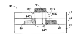
【解決手段】入口92Aと出口94Aのある複数のピンホール90Aを有する誘電領域14と、下側導電領域18とを備え、ピンホール90Aの少なくともいくつかは出口94A周辺において出口94Aより広い下側導電領域18のアンダーカット部96Aに面する誘電領域14の張り出し面98Aを持たせる
【選択図】図4
Description
誘電領域はまた、絶縁領域と呼ぶこともできる。たとえば、薄膜トランジスタに関する実施例において、誘電領域は、ゲート誘電体と呼ぶことができる。誘電領域は、有機および/または無機材料で構成できる。誘電領域に適した無機材料の例としては、酸化シリコン、窒化シリコン、酸化アルミニウム、チタン酸バリウム、チタン酸バリウムジルコニウム等がある。誘電領域のための有機ポリマの例としては、ポリエステル、ポリカーボネート、ポリ(ビニルフェノール)、ボリイミド、ポリスチレン、ポリ(メタクリレート)、ポリ(アクリレート)、エポキシ樹脂等がある。各種の実施例において、誘電領域は高分子誘電材料を含む。誘電領域は、プラズマ増強化学蒸着法、スパッタリングおよび、スピンコーティング、ディップコーティング、バーコーティング等の液体堆積法、インクジェット、スクリーン、フレキソグラフィ、グラビア印刷等の印刷法をはじめとして、好適であればどのような方法でも形成できる。好ましい実施例において、誘電領域は、液体堆積法で形成される。誘電領域の厚さは、使用される誘電材料の誘電率に応じて、たとえば、約10nmから約1000nmである。誘電領域の代表的な厚さは、約100nmから約500nmである。誘電領域は、たとえば、10-12S/cm未満または約10-10S/cm未満の伝導率を有していてもよい。
基板は、たとえば、シリコン、ガラス板、プラスチックフィルムまたはシート等で構成してもよい。構造的に柔軟なデバイスの場合、たとえば、ポリエステル、ポリカーボネート、ポリイミドシート等のプラスチック基板が好ましい。基板の厚さは約10マイクロメートルから約10ミリメートル以上であってもよく、特に柔軟なプラスチック基板についての厚さの例は約50から約100マイクロメートル、ガラス板やシリコンウェハ等の剛性の基板については約1から約10ミリメートルである。
ゲート電極は、薄い金属フィルム、伝導性ポリマフィルム、伝導性インクもしくはペーストで作製される伝導性フィルムであってもよく、あるいは基板そのものがゲート電極、たとえば高濃度にドーピングされたシリコンであってもよい。ゲート電極材料の例としては、これらに限定されないが、アルミニウム、金、銀、チタン、銅、クロム、インジウム錫酸化物や、スルフォン酸ポリスチレンをドーピングしたポリ(3,4−エチレンジオキシチオフェン)(PSS−PEDOT)等の伝導性ポリマや、カーボンブラック/グラファイトからなる伝導性インク/ペーストまたは、アチェソン・コロイド(Acheson Colloids)社から入手可能なエレクトロダグ(ELECTRODAG)(登録商標)等の高分子バインダ分散コロイド銀がある。ゲート電極は、真空蒸着、金属もしくは伝導性酸化金属のスパッタリング、スピンコーティングによる伝導性高分子溶液もしくは伝導性インクのコーティング、キャスティングまたは印刷によって作製できる。ゲート電極の厚さは、たとえば、金属フィルムの場合は約10から約200ナノメートルの範囲、高分子伝導体の場合は約1から約10マイクロメートルの範囲である。各種の実施例において、ゲート電極はパターニングされている。
各種の実施例において、半導体領域は半導体層と呼ばれる。有機半導体領域としての使用に適した材料には、アントラセン、テトラセン、ペンタセンおよび置換ペンタセン等のアセン、ペリレン、フラーレン、フタロシアニン、オリゴチオフェン、ポリチオフェンおよびこれらの置換誘導体等がある。各種の実施例において、有機半導体領域は、液体加工可能な材料で構成される。好適な半導体材料の例としては、ポリチオフェン、オリゴチオフェンおよび、米国特許出願第2003/0160234号として公開されている米国出願第10/042,342号および米国特許第6,621,099号、第6,774,393号、第6,770,904号に記載された半導体ポリマがあり、これらの開示はすべて、参照によって本願に援用される。さらに、好適な材料には、C.D.ディミトラコポーロスとP.R.L.マレンファントによるAdv. Mater., Vol. 12, No. 2, pp.99-117 (2002)の"Organic Thin Film Transistors for Large Area Electronics"に記載された半導体ポリマがあり、この開示もまた参照によって全体が本願に援用される。
下側導電領域には、好適であればどのようなエッチング液でも使用できる。このエッチング液は、誘電領域より下側導電領域をより急速にエッチングする(つまり、下側導電領域の優先的なエッチング)。各種の実施例において、誘電領域ではこのエッチング液によるエッチングはほとんど、またはまったく起こらない。代表的なエッチング液には、以下のものがある。HF,HNO3,HCl,H2SO4および酢酸等の酸、KOH,NaOHおよびNH3OH等の塩基、H2O2,(NH4)2S2O4ならびにそれらの混合物。たとえば、上記のエッチング液の異なる組み合わせで、異なる金属をエッチングすることができる。以下の表1は、一般的な金属のための代表的なエッチング液をまとめたものである。

厚さ約200nmの銅の層を真空蒸着によってガラス基板上に堆積させた。誘電体組成物は、0.08gのポリ(4ビニルフェノール)(PVP)と、PVPのためのクロスリンカとして0.08gのポリ(メラミンコフォルムアルデヒド)(メチル化、nブタノール中に84重量%)と、0.1gのポリ(メチルシルセスキオキサン)(pMSSQ)(nブタノール中に25重量%)を0.9gのnブタノール中に混合させることによって調製された。0.2ミクロンのシリンジフィルタでろ過した後に、この誘電体組成物を2000rpmで60秒間、銅層の上にスピンコーティングした。80℃で10分間乾燥させた後、誘電層に160℃で30分間、高温アニールとクロスリンクを行った。シャドウマスクを通して誘電層の上に金の電極を蒸着させることにより、20個のコンデンサを作った。コンデンサ測定器(capacitor meter)により、コンデンサの歩留まりは30%未満と測定された。
比較例1と同様にして銅層(下側導電領域)と誘電体が作製された。誘電層のクロスリンクを行った後、デバイスを0.1Mの(NH4)2S2O4水溶液中に浸漬し、誘電体層のピンホールを通じて銅層をアンダーカットした。エッチング後、誘電体を蒸留水、イソプロパノールで洗浄し、乾燥させた。アンダーカット部をまず顕微鏡で観察した。銅層がエッチングで除去され、光が通過するピンホールが明瞭に見えた。シャドウマスクを通して誘電層の上に金の電極(上側導電領域)を蒸着させることにより、20個のコンデンサを作った。歩留まりは100%と測定された。
ガラス基板上にボトムゲート・トップコンタクト式薄膜トランジスタを作製した。銅(〜200nm)をゲート電極として蒸着させた。ゲート誘電体は、比較例1と同様の銅ゲートの上に形成した。以下の化学式を有するポリチオフェンを半導体として使用した。
比較例2と同様の方法にエッチングを追加して、トランジスタを作製した。ゲート誘電層を熱によりクロスリンクさせた後に、デバイスをまず0.1Mの(NH4)2S2O4水溶液に2分間浸漬し、誘電層中のピンホールを通じて銅ゲート層をアンダーカットし、その後、蒸留水、イソプロパノールで洗浄し、空気乾燥させた。半導体層を堆積させ、ソース/ドレイン電極を蒸着させた後(上側導電領域に半導体層とソース/ドレイン電極がある)、このトランジスタを、ケースレー4200半導体特性測定装置を使って評価した。ほとんどのトランジスタが良好な性能を見せた。デバイス歩留まりは90%を超え、オフ電流は10-11Aのレベルと低く、電流オン/オフ比は約105であった。比較対象となるトランジスタに対し、オフ電流は有意に低く、電流オン/オフ比は格段に高かった。
Claims (3)
- 電子デバイスの製造方法であって、
(a)誘電領域と下側導電領域を設けるステップであって、前記誘電領域は各々入口と出口のある複数のピンホールを有するようにするステップと、
(b)前記ピンホールの中に前記下側導電領域のためのエッチング液を付着させ、前記ピンホールをアンダーカットして、いくつかの前記ピンホールについて、前記出口周辺において前記出口より広い前記下側導電領域のアンダーカット部に面する前記誘電領域の張り出し面を作るステップと、
を含むことを特徴とする方法。 - 電子デバイスであって、
(a)各々入口と出口のある複数のピンホールを有する誘電領域と、
(b)下側導電領域と、
を備え、前記ピンホールの少なくともいくつかは、前記出口周辺において前記出口より広い前記下側導電領域のアンダーカット部に面する前記誘電領域の張り出し面を持たせてアンダーカットされていることを特徴とする電子デバイス。 - 薄膜トランジスタであって、
(a)各々入口と出口のある複数のピンホールを有する誘電領域と、
(b)下側導電領域と、
を備え、前記ピンホールの少なくともいくつかは、前記出口周辺において前記出口より広い前記下側導電領域のアンダーカット部に面する前記誘電領域の張り出し面を持たせてアンダーカットされていることを特徴とする薄膜トランジスタ。
Applications Claiming Priority (1)
| Application Number | Priority Date | Filing Date | Title |
|---|---|---|---|
| US12/193,249 US7821068B2 (en) | 2008-08-18 | 2008-08-18 | Device and process involving pinhole undercut area |
Publications (2)
| Publication Number | Publication Date |
|---|---|
| JP2010045369A true JP2010045369A (ja) | 2010-02-25 |
| JP2010045369A5 JP2010045369A5 (ja) | 2012-09-27 |
Family
ID=41262208
Family Applications (1)
| Application Number | Title | Priority Date | Filing Date |
|---|---|---|---|
| JP2009187638A Pending JP2010045369A (ja) | 2008-08-18 | 2009-08-13 | ピンホールアンダーカット部を含む装置と工程 |
Country Status (6)
| Country | Link |
|---|---|
| US (1) | US7821068B2 (ja) |
| EP (1) | EP2157629A3 (ja) |
| JP (1) | JP2010045369A (ja) |
| KR (1) | KR20100021975A (ja) |
| CN (1) | CN101656294A (ja) |
| CA (1) | CA2675083C (ja) |
Families Citing this family (4)
| Publication number | Priority date | Publication date | Assignee | Title |
|---|---|---|---|---|
| KR101070289B1 (ko) * | 2009-12-30 | 2011-10-06 | 주식회사 하이닉스반도체 | 반도체 장치 제조방법 |
| US9076975B2 (en) | 2010-04-27 | 2015-07-07 | Xerox Corporation | Dielectric composition for thin-film transistors |
| TWI445180B (zh) * | 2011-09-28 | 2014-07-11 | E Ink Holdings Inc | 陣列基板及使用其之顯示裝置 |
| CN108039338A (zh) * | 2017-11-24 | 2018-05-15 | 华中科技大学 | 一种消除介质层针孔缺陷影响的方法 |
Citations (4)
| Publication number | Priority date | Publication date | Assignee | Title |
|---|---|---|---|---|
| JPS61183972A (ja) * | 1985-02-08 | 1986-08-16 | Matsushita Electric Ind Co Ltd | 薄膜半導体装置の製造方法 |
| JP2001281695A (ja) * | 2000-03-30 | 2001-10-10 | Sharp Corp | 薄膜静電容量の製造方法および液晶表示装置 |
| JP2007005782A (ja) * | 2005-05-27 | 2007-01-11 | Semiconductor Energy Lab Co Ltd | 半導体装置及び半導体装置の作製方法 |
| WO2008059633A1 (fr) * | 2006-11-15 | 2008-05-22 | Sharp Kabushiki Kaisha | Élément semi-conducteur, procédé de fabrication de celui-ci et affichage |
Family Cites Families (21)
| Publication number | Priority date | Publication date | Assignee | Title |
|---|---|---|---|---|
| DE2707959A1 (de) | 1977-02-24 | 1978-08-31 | Eberhard Loeffelholz | Skistock und skihandschuh halte- und fangvorrichtung |
| US5354695A (en) * | 1992-04-08 | 1994-10-11 | Leedy Glenn J | Membrane dielectric isolation IC fabrication |
| JP3200639B2 (ja) * | 1992-05-19 | 2001-08-20 | カシオ計算機株式会社 | 薄膜トランジスタパネルの製造方法 |
| TW232751B (en) * | 1992-10-09 | 1994-10-21 | Semiconductor Energy Res Co Ltd | Semiconductor device and method for forming the same |
| US5424233A (en) * | 1994-05-06 | 1995-06-13 | United Microflectronics Corporation | Method of making electrically programmable and erasable memory device with a depression |
| US6107117A (en) | 1996-12-20 | 2000-08-22 | Lucent Technologies Inc. | Method of making an organic thin film transistor |
| US6331722B1 (en) * | 1997-01-18 | 2001-12-18 | Semiconductor Energy Laboratory Co., Ltd. | Hybrid circuit and electronic device using same |
| JP4434411B2 (ja) * | 2000-02-16 | 2010-03-17 | 出光興産株式会社 | アクティブ駆動型有機el発光装置およびその製造方法 |
| JP4854866B2 (ja) * | 2001-04-27 | 2012-01-18 | 株式会社半導体エネルギー研究所 | 半導体装置の作製方法 |
| US6770904B2 (en) | 2002-01-11 | 2004-08-03 | Xerox Corporation | Polythiophenes and electronic devices generated therefrom |
| US6621099B2 (en) | 2002-01-11 | 2003-09-16 | Xerox Corporation | Polythiophenes and devices thereof |
| US6949762B2 (en) | 2002-01-11 | 2005-09-27 | Xerox Corporation | Polythiophenes and devices thereof |
| US20030227014A1 (en) | 2002-06-11 | 2003-12-11 | Xerox Corporation. | Process for forming semiconductor layer of micro-and nano-electronic devices |
| JP3532188B1 (ja) | 2002-10-21 | 2004-05-31 | 沖電気工業株式会社 | 半導体装置及びその製造方法 |
| US20060073613A1 (en) * | 2004-09-29 | 2006-04-06 | Sanjeev Aggarwal | Ferroelectric memory cells and methods for fabricating ferroelectric memory cells and ferroelectric capacitors thereof |
| US7205608B2 (en) * | 2005-07-25 | 2007-04-17 | Freescale Semiconductor, Inc. | Electronic device including discontinuous storage elements |
| JP2007073779A (ja) * | 2005-09-07 | 2007-03-22 | Elpida Memory Inc | 不揮発性メモリ素子及びその製造方法 |
| US20070128758A1 (en) * | 2005-12-01 | 2007-06-07 | Keisuke Tanaka | Semiconductor device and method for fabricating the same |
| US20070145453A1 (en) * | 2005-12-23 | 2007-06-28 | Xerox Corporation | Dielectric layer for electronic devices |
| US7488643B2 (en) * | 2006-06-21 | 2009-02-10 | International Business Machines Corporation | MIM capacitor and method of making same |
| US7855097B2 (en) * | 2008-07-11 | 2010-12-21 | Organicid, Inc. | Method of increasing yield in OFETs by using a high-K dielectric layer in a dual dielectric layer |
-
2008
- 2008-08-18 US US12/193,249 patent/US7821068B2/en active Active
-
2009
- 2009-08-11 CA CA2675083A patent/CA2675083C/en not_active Expired - Fee Related
- 2009-08-13 JP JP2009187638A patent/JP2010045369A/ja active Pending
- 2009-08-14 KR KR1020090075355A patent/KR20100021975A/ko not_active Application Discontinuation
- 2009-08-14 EP EP20090167865 patent/EP2157629A3/en not_active Withdrawn
- 2009-08-17 CN CN200910166517A patent/CN101656294A/zh active Pending
Patent Citations (4)
| Publication number | Priority date | Publication date | Assignee | Title |
|---|---|---|---|---|
| JPS61183972A (ja) * | 1985-02-08 | 1986-08-16 | Matsushita Electric Ind Co Ltd | 薄膜半導体装置の製造方法 |
| JP2001281695A (ja) * | 2000-03-30 | 2001-10-10 | Sharp Corp | 薄膜静電容量の製造方法および液晶表示装置 |
| JP2007005782A (ja) * | 2005-05-27 | 2007-01-11 | Semiconductor Energy Lab Co Ltd | 半導体装置及び半導体装置の作製方法 |
| WO2008059633A1 (fr) * | 2006-11-15 | 2008-05-22 | Sharp Kabushiki Kaisha | Élément semi-conducteur, procédé de fabrication de celui-ci et affichage |
Also Published As
| Publication number | Publication date |
|---|---|
| EP2157629A3 (en) | 2015-05-13 |
| CA2675083A1 (en) | 2010-02-18 |
| CN101656294A (zh) | 2010-02-24 |
| US20100038714A1 (en) | 2010-02-18 |
| KR20100021975A (ko) | 2010-02-26 |
| CA2675083C (en) | 2013-03-12 |
| US7821068B2 (en) | 2010-10-26 |
| EP2157629A2 (en) | 2010-02-24 |
Similar Documents
| Publication | Publication Date | Title |
|---|---|---|
| KR101508780B1 (ko) | 유기 박막 트랜지스터의 제조방법 및 그에 의해 제조된 유기 박막 트랜지스터 | |
| CN100514673C (zh) | 薄膜场效应晶体管及其制造方法 | |
| JP5221896B2 (ja) | 有機電子素子の電極形成方法、これによって形成された電極を含む有機薄膜トランジスタ及びこれを備えた表示素子 | |
| KR101282534B1 (ko) | 적층 구조체, 전자 소자, 및 표시 장치 | |
| JP5913107B2 (ja) | 有機半導体材料、有機半導体組成物、有機薄膜及び電界効果トランジスタ並びにその製造方法 | |
| JP2006295165A (ja) | 薄膜トランジスタ及び薄膜トランジスタの作製方法 | |
| JP2006295166A (ja) | 電子デバイス、薄膜トランジスタ及び薄膜トランジスタの作製方法 | |
| KR100981558B1 (ko) | 양극성 유기 전계 효과 박층 트랜지스터 및 그의 제조 방법 | |
| US9929345B1 (en) | Curable polymeric materials and their use for fabricating electronic devices | |
| JP5226715B2 (ja) | 有機薄膜トランジスタ、その作製方法、および、それに使用されるゲート絶縁層 | |
| TWI677104B (zh) | 薄膜電晶體、薄膜電晶體之製造方法及使用薄膜電晶體之影像顯示裝置 | |
| BRPI0016670B1 (pt) | método para configuração de um circuito eletrônico, e, circuito eletrônico | |
| US20170222168A1 (en) | Thin-film transistor and method of fabricating the same | |
| US9263686B2 (en) | Method of manufacturing organic thin film transistor having organic polymer insulating layer | |
| JP2010045369A (ja) | ピンホールアンダーカット部を含む装置と工程 | |
| KR101249097B1 (ko) | 유기절연막 조성물, 유기절연막의 형성방법 및 이에 의해형성된 유기절연막을 함유하는 유기박막 트랜지스터 | |
| KR101050588B1 (ko) | 유기절연막 패턴형성 방법 | |
| JP4360911B2 (ja) | 有機電子デバイス用の絶縁体 | |
| JP2007095777A (ja) | 有機半導体薄膜の製造方法及び有機半導体薄膜並びに電界効果トランジスタ | |
| TWI469224B (zh) | 有機薄膜電晶體及其製造方法 | |
| KR20180046257A (ko) | 박막 트랜지스터 제조 방법, 박막 트랜지스터, 및 이를 포함하는 전자 소자 | |
| JP2010056484A (ja) | 有機トランジスタ及び有機トランジスタの製造方法 | |
| JP2007238724A (ja) | 液状材料、膜付き基板の製造方法、電気光学装置の製造方法および電子機器の製造方法 | |
| TWI305961B (en) | Method of fabricating a electrical device | |
| JP5458296B2 (ja) | 微細加工構造及びその加工方法並びに電子デバイス及びその製造方法 |
Legal Events
| Date | Code | Title | Description |
|---|---|---|---|
| A521 | Request for written amendment filed |
Free format text: JAPANESE INTERMEDIATE CODE: A523 Effective date: 20120810 |
|
| A621 | Written request for application examination |
Free format text: JAPANESE INTERMEDIATE CODE: A621 Effective date: 20120810 |
|
| A871 | Explanation of circumstances concerning accelerated examination |
Free format text: JAPANESE INTERMEDIATE CODE: A871 Effective date: 20120810 |
|
| A975 | Report on accelerated examination |
Free format text: JAPANESE INTERMEDIATE CODE: A971005 Effective date: 20120828 |
|
| A131 | Notification of reasons for refusal |
Free format text: JAPANESE INTERMEDIATE CODE: A131 Effective date: 20120904 |
|
| A521 | Request for written amendment filed |
Free format text: JAPANESE INTERMEDIATE CODE: A523 Effective date: 20121121 |
|
| A131 | Notification of reasons for refusal |
Free format text: JAPANESE INTERMEDIATE CODE: A131 Effective date: 20130122 |
|
| A521 | Request for written amendment filed |
Free format text: JAPANESE INTERMEDIATE CODE: A523 Effective date: 20130408 |
|
| A02 | Decision of refusal |
Free format text: JAPANESE INTERMEDIATE CODE: A02 Effective date: 20130618 |
|
| RD02 | Notification of acceptance of power of attorney |
Free format text: JAPANESE INTERMEDIATE CODE: A7422 Effective date: 20130801 |
|
| A711 | Notification of change in applicant |
Free format text: JAPANESE INTERMEDIATE CODE: A711 Effective date: 20130802 |