JP2010027883A - 半導体集積回路装置 - Google Patents
半導体集積回路装置 Download PDFInfo
- Publication number
- JP2010027883A JP2010027883A JP2008188144A JP2008188144A JP2010027883A JP 2010027883 A JP2010027883 A JP 2010027883A JP 2008188144 A JP2008188144 A JP 2008188144A JP 2008188144 A JP2008188144 A JP 2008188144A JP 2010027883 A JP2010027883 A JP 2010027883A
- Authority
- JP
- Japan
- Prior art keywords
- integrated circuit
- circuit device
- semiconductor integrated
- wiring
- power supply
- Prior art date
- Legal status (The legal status is an assumption and is not a legal conclusion. Google has not performed a legal analysis and makes no representation as to the accuracy of the status listed.)
- Granted
Links
Images


Classifications
-
- H—ELECTRICITY
- H01—ELECTRIC ELEMENTS
- H01L—SEMICONDUCTOR DEVICES NOT COVERED BY CLASS H10
- H01L27/00—Devices consisting of a plurality of semiconductor or other solid-state components formed in or on a common substrate
- H01L27/02—Devices consisting of a plurality of semiconductor or other solid-state components formed in or on a common substrate including semiconductor components specially adapted for rectifying, oscillating, amplifying or switching and having at least one potential-jump barrier or surface barrier; including integrated passive circuit elements with at least one potential-jump barrier or surface barrier
- H01L27/0203—Particular design considerations for integrated circuits
- H01L27/0207—Geometrical layout of the components, e.g. computer aided design; custom LSI, semi-custom LSI, standard cell technique
-
- G—PHYSICS
- G11—INFORMATION STORAGE
- G11C—STATIC STORES
- G11C16/00—Erasable programmable read-only memories
- G11C16/02—Erasable programmable read-only memories electrically programmable
- G11C16/06—Auxiliary circuits, e.g. for writing into memory
- G11C16/30—Power supply circuits
-
- H—ELECTRICITY
- H01—ELECTRIC ELEMENTS
- H01L—SEMICONDUCTOR DEVICES NOT COVERED BY CLASS H10
- H01L23/00—Details of semiconductor or other solid state devices
- H01L23/48—Arrangements for conducting electric current to or from the solid state body in operation, e.g. leads, terminal arrangements ; Selection of materials therefor
- H01L23/482—Arrangements for conducting electric current to or from the solid state body in operation, e.g. leads, terminal arrangements ; Selection of materials therefor consisting of lead-in layers inseparably applied to the semiconductor body
- H01L23/4824—Pads with extended contours, e.g. grid structure, branch structure, finger structure
-
- H—ELECTRICITY
- H01—ELECTRIC ELEMENTS
- H01L—SEMICONDUCTOR DEVICES NOT COVERED BY CLASS H10
- H01L27/00—Devices consisting of a plurality of semiconductor or other solid-state components formed in or on a common substrate
- H01L27/02—Devices consisting of a plurality of semiconductor or other solid-state components formed in or on a common substrate including semiconductor components specially adapted for rectifying, oscillating, amplifying or switching and having at least one potential-jump barrier or surface barrier; including integrated passive circuit elements with at least one potential-jump barrier or surface barrier
- H01L27/0203—Particular design considerations for integrated circuits
- H01L27/0214—Particular design considerations for integrated circuits for internal polarisation, e.g. I2L
- H01L27/0218—Particular design considerations for integrated circuits for internal polarisation, e.g. I2L of field effect structures
-
- H—ELECTRICITY
- H10—SEMICONDUCTOR DEVICES; ELECTRIC SOLID-STATE DEVICES NOT OTHERWISE PROVIDED FOR
- H10B—ELECTRONIC MEMORY DEVICES
- H10B41/00—Electrically erasable-and-programmable ROM [EEPROM] devices comprising floating gates
- H10B41/40—Electrically erasable-and-programmable ROM [EEPROM] devices comprising floating gates characterised by the peripheral circuit region
-
- H—ELECTRICITY
- H10—SEMICONDUCTOR DEVICES; ELECTRIC SOLID-STATE DEVICES NOT OTHERWISE PROVIDED FOR
- H10B—ELECTRONIC MEMORY DEVICES
- H10B43/00—EEPROM devices comprising charge-trapping gate insulators
- H10B43/40—EEPROM devices comprising charge-trapping gate insulators characterised by the peripheral circuit region
-
- H—ELECTRICITY
- H01—ELECTRIC ELEMENTS
- H01L—SEMICONDUCTOR DEVICES NOT COVERED BY CLASS H10
- H01L2224/00—Indexing scheme for arrangements for connecting or disconnecting semiconductor or solid-state bodies and methods related thereto as covered by H01L24/00
- H01L2224/01—Means for bonding being attached to, or being formed on, the surface to be connected, e.g. chip-to-package, die-attach, "first-level" interconnects; Manufacturing methods related thereto
- H01L2224/42—Wire connectors; Manufacturing methods related thereto
- H01L2224/47—Structure, shape, material or disposition of the wire connectors after the connecting process
- H01L2224/48—Structure, shape, material or disposition of the wire connectors after the connecting process of an individual wire connector
- H01L2224/4805—Shape
- H01L2224/4809—Loop shape
- H01L2224/48091—Arched
-
- H—ELECTRICITY
- H01—ELECTRIC ELEMENTS
- H01L—SEMICONDUCTOR DEVICES NOT COVERED BY CLASS H10
- H01L2224/00—Indexing scheme for arrangements for connecting or disconnecting semiconductor or solid-state bodies and methods related thereto as covered by H01L24/00
- H01L2224/01—Means for bonding being attached to, or being formed on, the surface to be connected, e.g. chip-to-package, die-attach, "first-level" interconnects; Manufacturing methods related thereto
- H01L2224/42—Wire connectors; Manufacturing methods related thereto
- H01L2224/47—Structure, shape, material or disposition of the wire connectors after the connecting process
- H01L2224/48—Structure, shape, material or disposition of the wire connectors after the connecting process of an individual wire connector
- H01L2224/481—Disposition
- H01L2224/48151—Connecting between a semiconductor or solid-state body and an item not being a semiconductor or solid-state body, e.g. chip-to-substrate, chip-to-passive
- H01L2224/48221—Connecting between a semiconductor or solid-state body and an item not being a semiconductor or solid-state body, e.g. chip-to-substrate, chip-to-passive the body and the item being stacked
- H01L2224/48225—Connecting between a semiconductor or solid-state body and an item not being a semiconductor or solid-state body, e.g. chip-to-substrate, chip-to-passive the body and the item being stacked the item being non-metallic, e.g. insulating substrate with or without metallisation
- H01L2224/48227—Connecting between a semiconductor or solid-state body and an item not being a semiconductor or solid-state body, e.g. chip-to-substrate, chip-to-passive the body and the item being stacked the item being non-metallic, e.g. insulating substrate with or without metallisation connecting the wire to a bond pad of the item
-
- H—ELECTRICITY
- H01—ELECTRIC ELEMENTS
- H01L—SEMICONDUCTOR DEVICES NOT COVERED BY CLASS H10
- H01L2924/00—Indexing scheme for arrangements or methods for connecting or disconnecting semiconductor or solid-state bodies as covered by H01L24/00
- H01L2924/0001—Technical content checked by a classifier
- H01L2924/0002—Not covered by any one of groups H01L24/00, H01L24/00 and H01L2224/00
-
- H—ELECTRICITY
- H01—ELECTRIC ELEMENTS
- H01L—SEMICONDUCTOR DEVICES NOT COVERED BY CLASS H10
- H01L2924/00—Indexing scheme for arrangements or methods for connecting or disconnecting semiconductor or solid-state bodies as covered by H01L24/00
- H01L2924/19—Details of hybrid assemblies other than the semiconductor or other solid state devices to be connected
- H01L2924/191—Disposition
- H01L2924/19101—Disposition of discrete passive components
- H01L2924/19107—Disposition of discrete passive components off-chip wires
Landscapes
- Engineering & Computer Science (AREA)
- Power Engineering (AREA)
- Physics & Mathematics (AREA)
- Condensed Matter Physics & Semiconductors (AREA)
- General Physics & Mathematics (AREA)
- Computer Hardware Design (AREA)
- Microelectronics & Electronic Packaging (AREA)
- General Engineering & Computer Science (AREA)
- Semiconductor Integrated Circuits (AREA)
Abstract
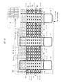
【解決手段】メモリ用電源部13は、複数のトランジスタ、および誤差増幅器からなる。トランジスタのソースパッドS、およびドレインパッドDは、それぞれ交互に一列となるように半導体チップの任意の一辺の周辺部に沿って配列されている。また、トランジスタのゲートは、それぞれ交互に配列されたソースパッドS、およびドレインパッドDと平行するように(ソースパッドS、およびドレインパッドDの配列方向とゲートの長辺方向とが平行となる)形成されている。これにより、ドレイン、ソースと接続される配線の配線距離を短くすることが可能となり、シート抵抗を削減することができる。
【選択図】図2
Description
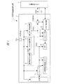
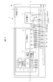
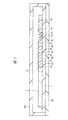
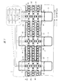
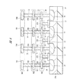
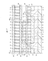
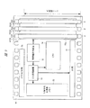
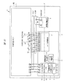
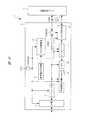
図1は、本発明の実施の形態1による半導体集積回路装置の構成例を示すブロック図、図2は、図1の半導体集積回路装置における実装レイアウトの一例を示す説明図、図3は、図2のA−A’断面図、図4は、図1の半導体集積回路装置に設けられたメモリ用電源部におけるソースパッドとドレインパッドとの配列パターン、および接続構成の一例を示す説明図、図5は、図4のメモリ用電源部におけるトランジスタのレイアウトパターンの一例を示す説明図、図6は、図5のA−A’断面図、図7は、図5のB−B’断面図、図8は、図4のメモリ用電源部におけるドレイン配線とソース配線とのレイアウト例を示す説明図、図9は、本発明者が検討したメモリ用電源部におけるドレイン配線とソース配線とのレイアウト例を示す説明図である。
図10は、本発明の実施の形態2による半導体集積回路装置における実装レイアウトの一例を示す説明図、図11は、図10のA−A’断面図である。
図12は、本実施の形態3によるメモリ用電源部におけるソースパッド、およびドレインパッドの配列パターン、および接続構成の一例を示す説明図、図13は、図12のメモリ用電源部におけるトランジスタのレイアウトパターンの一例を示す説明図、図14は、図13のA−A’断面図、図15は、図13のB−B’断面図である。
図16は、本発明の実施の形態4によるメモリ用電源部におけるトランジスタのレイアウトパターンの一例を示す説明図、図17は、図16のA−A’断面図、図18は、図16のB−B’断面図である。
2 マイクロコンピュータ
3 不揮発性メモリ
4 静電容量素子
5 I/O部
6,7 レベルシフタ
8 基準電圧生成部
9 不揮発性半導体メモリ
10 CPU
11 CPU用電源部
12 メモリ用I/O部
13 メモリ用電源部
14 半導体基板
14a N−WELL
15 P−WELL
16 P−WELL
17 ゲート
18 コンタクト
19 ビア
20 コンタクト
21 ビア
22 コンタクト
PK パッケージ基板
VCCPAD 電源パッド
VDDPAD 電源パッド
VDDP 電源配線
VCCP 電源配線
S ソースパッド
D ドレインパッド
B1〜B4 ボンディングワイヤ
T トランジスタ
OP 誤差増幅器
M1〜M3 配線層
SH ソース配線
GH ゲート配線
DH ドレイン配線
50 マイクロコンピュータ
51 I/O部
52 基準電圧生成部
53 不揮発性半導体メモリ
54 CPU
55 CPU用電源部
56 メモリ用I/O部
S10 ソースパッド
D10 ドレインパッド
Claims (8)
- 直流の電源電圧を任意の直流電圧に変換するレギュレータを備えた半導体集積回路装置であって、
前記レギュレータは、
複数のトランジスタからなる出力ドライバと、
前記トランジスタのソースに電源電圧を供給する入力電圧パッドと、
前記トランジスタのドレインに接続され、任意の直流電圧を出力する出力電圧パッドとを備え、
前記入力電圧パッド、および前記出力電圧パッドは、
前記レギュレータが形成された半導体チップの任意の一辺に沿って、直線状に配列されて形成され、
前記トランジスタのゲートは、
前記入力電圧パッド、および前記出力電圧パッドの配列と平行するように形成されていることを特徴とする半導体集積回路装置。 - 請求項1記載の半導体集積回路装置において、
前記入力電圧パッドに接続された第1の幹線と、
前記第1の幹線から延在し、前記トランジスタの第1の拡散層に電圧を供給する第1の支線と、
前記出力電圧パッドに接続された第2の幹線と、
前記第2の幹線から延在し、前記トランジスタの第2の拡散層から前記出力電圧パッドに電圧を供給する第2の支線とを備え、
前記第1、および前記第2の支線は、
前記入力電圧パッド、および前記出力電圧パッドの配列と平行するように形成されていることを特徴とする半導体集積回路装置。 - 請求項1または2記載の半導体集積回路装置において、
前記入力電圧パッドと前記出力電圧パッドとは、交互にレイアウトされて配列されていることを特徴とする半導体集積回路装置。 - 請求項1または2記載の半導体集積回路装置において、
複数の前記入力電圧パッドは、第1のグループとして直線状に配列され、
複数の前記出力電圧パッドは、第2のグループとして直線状に配列され、
前記第1のグループ、および前記第2のグループが直線状に配列されてレイアウトされていることを特徴とする半導体集積回路装置。 - 請求項1〜4のいずれか1項に記載の半導体集積回路装置において、
複数の前記トランジスタは、
ソース、ドレイン、およびゲートがそれぞれ共通に接続された並列接続された構成よりなることを特徴とする半導体集積回路装置。 - 請求項1〜5のいずれか1項に記載の半導体集積回路装置において、
前記半導体集積回路装置は、
少なくとも2つの半導体チップを搭載したシステムインパッケージからなり、
前記レギュレータは、
前記レギュレータが備えられていない他の前記半導体チップ、または前記半導体集積回路装置に外部接続された他の半導体チップに対して、変換した任意の直流電圧を供給することを特徴とする半導体集積回路装置。 - 請求項1〜5のいずれか1項に記載の半導体集積回路装置において、
前記レギュレータは、
前記半導体集積回路装置に外部接続された他の半導体チップに対して、変換した任意の直流電圧を供給することを特徴とする半導体集積回路装置。 - 請求項1〜7のいずれか1項に記載の半導体集積回路装置において、
前記半導体集積回路装置は、
CPUを有したコントローラであることを特徴とする半導体集積回路装置。
Priority Applications (5)
| Application Number | Priority Date | Filing Date | Title |
|---|---|---|---|
| JP2008188144A JP5363044B2 (ja) | 2008-07-22 | 2008-07-22 | 半導体集積回路装置 |
| US12/475,867 US7872520B2 (en) | 2008-07-22 | 2009-06-01 | Semiconductor integrated circuit device |
| TW098121504A TW201017867A (en) | 2008-07-22 | 2009-06-26 | Semiconductor integrated circuit device |
| CN200910149191.7A CN101635506B (zh) | 2008-07-22 | 2009-06-26 | 半导体集成电路器件 |
| US12/980,140 US8063695B2 (en) | 2008-07-22 | 2010-12-28 | Semiconductor integrated circuit device |
Applications Claiming Priority (1)
| Application Number | Priority Date | Filing Date | Title |
|---|---|---|---|
| JP2008188144A JP5363044B2 (ja) | 2008-07-22 | 2008-07-22 | 半導体集積回路装置 |
Publications (2)
| Publication Number | Publication Date |
|---|---|
| JP2010027883A true JP2010027883A (ja) | 2010-02-04 |
| JP5363044B2 JP5363044B2 (ja) | 2013-12-11 |
Family
ID=41568095
Family Applications (1)
| Application Number | Title | Priority Date | Filing Date |
|---|---|---|---|
| JP2008188144A Expired - Fee Related JP5363044B2 (ja) | 2008-07-22 | 2008-07-22 | 半導体集積回路装置 |
Country Status (4)
| Country | Link |
|---|---|
| US (2) | US7872520B2 (ja) |
| JP (1) | JP5363044B2 (ja) |
| CN (1) | CN101635506B (ja) |
| TW (1) | TW201017867A (ja) |
Families Citing this family (8)
| Publication number | Priority date | Publication date | Assignee | Title |
|---|---|---|---|---|
| CA2674038C (en) | 2006-12-28 | 2015-12-01 | Argentumcidalelectrics, Inc. | Ex vivo antimicrobial devices and methods |
| KR20130092110A (ko) * | 2012-02-10 | 2013-08-20 | 삼성전자주식회사 | 임베디드 솔리드 스테이트 디스크 및 솔리드 스테이트 디스크 |
| JP2015170658A (ja) * | 2014-03-05 | 2015-09-28 | マイクロン テクノロジー, インク. | 半導体装置 |
| JP2018133503A (ja) * | 2017-02-16 | 2018-08-23 | 東芝メモリ株式会社 | 半導体記憶装置 |
| WO2018180010A1 (ja) * | 2017-03-29 | 2018-10-04 | 株式会社ソシオネクスト | 半導体集積回路装置 |
| CN110047813B (zh) * | 2018-01-15 | 2021-04-06 | 联华电子股份有限公司 | 半导体元件 |
| KR20210128681A (ko) * | 2020-04-17 | 2021-10-27 | 에스케이하이닉스 주식회사 | 저항 소자를 구비하는 반도체 장치 |
| CN112088406B (zh) * | 2020-08-06 | 2023-10-03 | 长江存储科技有限责任公司 | 用于三维存储器的多管芯峰值功率管理 |
Citations (3)
| Publication number | Priority date | Publication date | Assignee | Title |
|---|---|---|---|---|
| JPS60152038A (ja) * | 1984-01-20 | 1985-08-10 | Toshiba Corp | GaAsゲ−トアレイ集積回路 |
| JP2004193475A (ja) * | 2002-12-13 | 2004-07-08 | Ricoh Co Ltd | 電源用ic及びその電源用icを使用した通信装置 |
| JP2007149885A (ja) * | 2005-11-25 | 2007-06-14 | Sanyo Electric Co Ltd | 化合物半導体スイッチ回路装置およびその製造方法 |
Family Cites Families (5)
| Publication number | Priority date | Publication date | Assignee | Title |
|---|---|---|---|---|
| JP2002008374A (ja) * | 2000-06-22 | 2002-01-11 | Mitsubishi Electric Corp | 電圧降圧回路 |
| US7138698B2 (en) * | 2003-12-18 | 2006-11-21 | Kabushiki Kaisha Toshiba | Semiconductor device including power MOS field-effect transistor and driver circuit driving thereof |
| US7112855B2 (en) * | 2004-05-07 | 2006-09-26 | Broadcom Corporation | Low ohmic layout technique for MOS transistors |
| JP5143413B2 (ja) * | 2006-12-20 | 2013-02-13 | オンセミコンダクター・トレーディング・リミテッド | 半導体集積回路 |
| US7728565B2 (en) * | 2007-11-12 | 2010-06-01 | Itt Manufacturing Enterprises, Inc. | Non-invasive load current sensing in low dropout (LDO) regulators |
-
2008
- 2008-07-22 JP JP2008188144A patent/JP5363044B2/ja not_active Expired - Fee Related
-
2009
- 2009-06-01 US US12/475,867 patent/US7872520B2/en active Active
- 2009-06-26 CN CN200910149191.7A patent/CN101635506B/zh not_active Expired - Fee Related
- 2009-06-26 TW TW098121504A patent/TW201017867A/zh unknown
-
2010
- 2010-12-28 US US12/980,140 patent/US8063695B2/en active Active
Patent Citations (3)
| Publication number | Priority date | Publication date | Assignee | Title |
|---|---|---|---|---|
| JPS60152038A (ja) * | 1984-01-20 | 1985-08-10 | Toshiba Corp | GaAsゲ−トアレイ集積回路 |
| JP2004193475A (ja) * | 2002-12-13 | 2004-07-08 | Ricoh Co Ltd | 電源用ic及びその電源用icを使用した通信装置 |
| JP2007149885A (ja) * | 2005-11-25 | 2007-06-14 | Sanyo Electric Co Ltd | 化合物半導体スイッチ回路装置およびその製造方法 |
Also Published As
| Publication number | Publication date |
|---|---|
| TW201017867A (en) | 2010-05-01 |
| US7872520B2 (en) | 2011-01-18 |
| CN101635506B (zh) | 2016-08-17 |
| US20110090001A1 (en) | 2011-04-21 |
| JP5363044B2 (ja) | 2013-12-11 |
| US8063695B2 (en) | 2011-11-22 |
| CN101635506A (zh) | 2010-01-27 |
| US20100019835A1 (en) | 2010-01-28 |
Similar Documents
| Publication | Publication Date | Title |
|---|---|---|
| JP5363044B2 (ja) | 半導体集積回路装置 | |
| JP4969934B2 (ja) | 半導体装置 | |
| JP4841204B2 (ja) | 半導体装置 | |
| US8878351B2 (en) | Semiconductor device | |
| JP3433731B2 (ja) | I/oセル配置方法及び半導体装置 | |
| JP2010147282A (ja) | 半導体集積回路装置 | |
| JP2012114241A (ja) | 半導体チップおよび半導体装置 | |
| JP2007066922A (ja) | 半導体集積回路装置 | |
| KR101016463B1 (ko) | 반도체 집적 회로 | |
| US20060001131A1 (en) | Memory device power distribution in memory assemblies | |
| CN112771655A (zh) | 半导体集成电路装置以及半导体封装件构造 | |
| JP4577690B2 (ja) | 半導体装置 | |
| JP5264135B2 (ja) | 半導体集積回路及びマルチチップモジュール | |
| JP2012235048A (ja) | 半導体装置 | |
| US8507994B2 (en) | Semiconductor device | |
| JP2003243538A (ja) | 半導体集積回路装置 | |
| JP2010161158A (ja) | 半導体集積回路装置 | |
| CN112567507A (zh) | 半导体集成电路装置 | |
| JP4921724B2 (ja) | 半導体装置におけるパッド部の配線構造 | |
| JP5168872B2 (ja) | 半導体集積回路 | |
| JP5604602B2 (ja) | 半導体集積回路装置 | |
| JP4175155B2 (ja) | 半導体装置 | |
| US10833011B2 (en) | Semiconductor device | |
| JP2012243810A (ja) | 半導体集積回路装置 | |
| JP2008218751A (ja) | 半導体装置及びi/oセル |
Legal Events
| Date | Code | Title | Description |
|---|---|---|---|
| A711 | Notification of change in applicant |
Free format text: JAPANESE INTERMEDIATE CODE: A712 Effective date: 20100528 |
|
| A621 | Written request for application examination |
Free format text: JAPANESE INTERMEDIATE CODE: A621 Effective date: 20110712 |
|
| A977 | Report on retrieval |
Free format text: JAPANESE INTERMEDIATE CODE: A971007 Effective date: 20130502 |
|
| A131 | Notification of reasons for refusal |
Free format text: JAPANESE INTERMEDIATE CODE: A131 Effective date: 20130528 |
|
| A521 | Request for written amendment filed |
Free format text: JAPANESE INTERMEDIATE CODE: A523 Effective date: 20130725 |
|
| TRDD | Decision of grant or rejection written | ||
| A01 | Written decision to grant a patent or to grant a registration (utility model) |
Free format text: JAPANESE INTERMEDIATE CODE: A01 Effective date: 20130813 |
|
| A61 | First payment of annual fees (during grant procedure) |
Free format text: JAPANESE INTERMEDIATE CODE: A61 Effective date: 20130905 |
|
| R150 | Certificate of patent or registration of utility model |
Ref document number: 5363044 Country of ref document: JP Free format text: JAPANESE INTERMEDIATE CODE: R150 Free format text: JAPANESE INTERMEDIATE CODE: R150 |
|
| S531 | Written request for registration of change of domicile |
Free format text: JAPANESE INTERMEDIATE CODE: R313531 |
|
| R350 | Written notification of registration of transfer |
Free format text: JAPANESE INTERMEDIATE CODE: R350 |
|
| LAPS | Cancellation because of no payment of annual fees |