JP2010021585A - 半導体発光装置の製造方法 - Google Patents
半導体発光装置の製造方法 Download PDFInfo
- Publication number
- JP2010021585A JP2010021585A JP2009245841A JP2009245841A JP2010021585A JP 2010021585 A JP2010021585 A JP 2010021585A JP 2009245841 A JP2009245841 A JP 2009245841A JP 2009245841 A JP2009245841 A JP 2009245841A JP 2010021585 A JP2010021585 A JP 2010021585A
- Authority
- JP
- Japan
- Prior art keywords
- light emitting
- layer
- substrate
- laser
- cladding layer
- Prior art date
- Legal status (The legal status is an assumption and is not a legal conclusion. Google has not performed a legal analysis and makes no representation as to the accuracy of the status listed.)
- Granted
Links
Images


Classifications
-
- G—PHYSICS
- G11—INFORMATION STORAGE
- G11B—INFORMATION STORAGE BASED ON RELATIVE MOVEMENT BETWEEN RECORD CARRIER AND TRANSDUCER
- G11B7/00—Recording or reproducing by optical means, e.g. recording using a thermal beam of optical radiation by modifying optical properties or the physical structure, reproducing using an optical beam at lower power by sensing optical properties; Record carriers therefor
- G11B7/12—Heads, e.g. forming of the optical beam spot or modulation of the optical beam
- G11B7/125—Optical beam sources therefor, e.g. laser control circuitry specially adapted for optical storage devices; Modulators, e.g. means for controlling the size or intensity of optical spots or optical traces
- G11B7/126—Circuits, methods or arrangements for laser control or stabilisation
-
- B—PERFORMING OPERATIONS; TRANSPORTING
- B82—NANOTECHNOLOGY
- B82Y—SPECIFIC USES OR APPLICATIONS OF NANOSTRUCTURES; MEASUREMENT OR ANALYSIS OF NANOSTRUCTURES; MANUFACTURE OR TREATMENT OF NANOSTRUCTURES
- B82Y20/00—Nanooptics, e.g. quantum optics or photonic crystals
-
- G—PHYSICS
- G11—INFORMATION STORAGE
- G11B—INFORMATION STORAGE BASED ON RELATIVE MOVEMENT BETWEEN RECORD CARRIER AND TRANSDUCER
- G11B7/00—Recording or reproducing by optical means, e.g. recording using a thermal beam of optical radiation by modifying optical properties or the physical structure, reproducing using an optical beam at lower power by sensing optical properties; Record carriers therefor
- G11B7/12—Heads, e.g. forming of the optical beam spot or modulation of the optical beam
- G11B7/125—Optical beam sources therefor, e.g. laser control circuitry specially adapted for optical storage devices; Modulators, e.g. means for controlling the size or intensity of optical spots or optical traces
- G11B7/127—Lasers; Multiple laser arrays
- G11B7/1275—Two or more lasers having different wavelengths
-
- H—ELECTRICITY
- H01—ELECTRIC ELEMENTS
- H01S—DEVICES USING THE PROCESS OF LIGHT AMPLIFICATION BY STIMULATED EMISSION OF RADIATION [LASER] TO AMPLIFY OR GENERATE LIGHT; DEVICES USING STIMULATED EMISSION OF ELECTROMAGNETIC RADIATION IN WAVE RANGES OTHER THAN OPTICAL
- H01S5/00—Semiconductor lasers
- H01S5/02—Structural details or components not essential to laser action
- H01S5/026—Monolithically integrated components, e.g. waveguides, monitoring photo-detectors, drivers
-
- H—ELECTRICITY
- H01—ELECTRIC ELEMENTS
- H01S—DEVICES USING THE PROCESS OF LIGHT AMPLIFICATION BY STIMULATED EMISSION OF RADIATION [LASER] TO AMPLIFY OR GENERATE LIGHT; DEVICES USING STIMULATED EMISSION OF ELECTROMAGNETIC RADIATION IN WAVE RANGES OTHER THAN OPTICAL
- H01S5/00—Semiconductor lasers
- H01S5/20—Structure or shape of the semiconductor body to guide the optical wave ; Confining structures perpendicular to the optical axis, e.g. index or gain guiding, stripe geometry, broad area lasers, gain tailoring, transverse or lateral reflectors, special cladding structures, MQW barrier reflection layers
- H01S5/22—Structure or shape of the semiconductor body to guide the optical wave ; Confining structures perpendicular to the optical axis, e.g. index or gain guiding, stripe geometry, broad area lasers, gain tailoring, transverse or lateral reflectors, special cladding structures, MQW barrier reflection layers having a ridge or stripe structure
-
- H—ELECTRICITY
- H01—ELECTRIC ELEMENTS
- H01S—DEVICES USING THE PROCESS OF LIGHT AMPLIFICATION BY STIMULATED EMISSION OF RADIATION [LASER] TO AMPLIFY OR GENERATE LIGHT; DEVICES USING STIMULATED EMISSION OF ELECTROMAGNETIC RADIATION IN WAVE RANGES OTHER THAN OPTICAL
- H01S5/00—Semiconductor lasers
- H01S5/30—Structure or shape of the active region; Materials used for the active region
- H01S5/32—Structure or shape of the active region; Materials used for the active region comprising PN junctions, e.g. hetero- or double- heterostructures
- H01S5/323—Structure or shape of the active region; Materials used for the active region comprising PN junctions, e.g. hetero- or double- heterostructures in AIIIBV compounds, e.g. AlGaAs-laser, InP-based laser
-
- H—ELECTRICITY
- H01—ELECTRIC ELEMENTS
- H01S—DEVICES USING THE PROCESS OF LIGHT AMPLIFICATION BY STIMULATED EMISSION OF RADIATION [LASER] TO AMPLIFY OR GENERATE LIGHT; DEVICES USING STIMULATED EMISSION OF ELECTROMAGNETIC RADIATION IN WAVE RANGES OTHER THAN OPTICAL
- H01S5/00—Semiconductor lasers
- H01S5/20—Structure or shape of the semiconductor body to guide the optical wave ; Confining structures perpendicular to the optical axis, e.g. index or gain guiding, stripe geometry, broad area lasers, gain tailoring, transverse or lateral reflectors, special cladding structures, MQW barrier reflection layers
- H01S5/22—Structure or shape of the semiconductor body to guide the optical wave ; Confining structures perpendicular to the optical axis, e.g. index or gain guiding, stripe geometry, broad area lasers, gain tailoring, transverse or lateral reflectors, special cladding structures, MQW barrier reflection layers having a ridge or stripe structure
- H01S5/2201—Structure or shape of the semiconductor body to guide the optical wave ; Confining structures perpendicular to the optical axis, e.g. index or gain guiding, stripe geometry, broad area lasers, gain tailoring, transverse or lateral reflectors, special cladding structures, MQW barrier reflection layers having a ridge or stripe structure in a specific crystallographic orientation
-
- H—ELECTRICITY
- H01—ELECTRIC ELEMENTS
- H01S—DEVICES USING THE PROCESS OF LIGHT AMPLIFICATION BY STIMULATED EMISSION OF RADIATION [LASER] TO AMPLIFY OR GENERATE LIGHT; DEVICES USING STIMULATED EMISSION OF ELECTROMAGNETIC RADIATION IN WAVE RANGES OTHER THAN OPTICAL
- H01S5/00—Semiconductor lasers
- H01S5/30—Structure or shape of the active region; Materials used for the active region
- H01S5/34—Structure or shape of the active region; Materials used for the active region comprising quantum well or superlattice structures, e.g. single quantum well [SQW] lasers, multiple quantum well [MQW] lasers or graded index separate confinement heterostructure [GRINSCH] lasers
- H01S5/343—Structure or shape of the active region; Materials used for the active region comprising quantum well or superlattice structures, e.g. single quantum well [SQW] lasers, multiple quantum well [MQW] lasers or graded index separate confinement heterostructure [GRINSCH] lasers in AIIIBV compounds, e.g. AlGaAs-laser, InP-based laser
- H01S5/34313—Structure or shape of the active region; Materials used for the active region comprising quantum well or superlattice structures, e.g. single quantum well [SQW] lasers, multiple quantum well [MQW] lasers or graded index separate confinement heterostructure [GRINSCH] lasers in AIIIBV compounds, e.g. AlGaAs-laser, InP-based laser with a well layer having only As as V-compound, e.g. AlGaAs, InGaAs
-
- H—ELECTRICITY
- H01—ELECTRIC ELEMENTS
- H01S—DEVICES USING THE PROCESS OF LIGHT AMPLIFICATION BY STIMULATED EMISSION OF RADIATION [LASER] TO AMPLIFY OR GENERATE LIGHT; DEVICES USING STIMULATED EMISSION OF ELECTROMAGNETIC RADIATION IN WAVE RANGES OTHER THAN OPTICAL
- H01S5/00—Semiconductor lasers
- H01S5/30—Structure or shape of the active region; Materials used for the active region
- H01S5/34—Structure or shape of the active region; Materials used for the active region comprising quantum well or superlattice structures, e.g. single quantum well [SQW] lasers, multiple quantum well [MQW] lasers or graded index separate confinement heterostructure [GRINSCH] lasers
- H01S5/343—Structure or shape of the active region; Materials used for the active region comprising quantum well or superlattice structures, e.g. single quantum well [SQW] lasers, multiple quantum well [MQW] lasers or graded index separate confinement heterostructure [GRINSCH] lasers in AIIIBV compounds, e.g. AlGaAs-laser, InP-based laser
- H01S5/34326—Structure or shape of the active region; Materials used for the active region comprising quantum well or superlattice structures, e.g. single quantum well [SQW] lasers, multiple quantum well [MQW] lasers or graded index separate confinement heterostructure [GRINSCH] lasers in AIIIBV compounds, e.g. AlGaAs-laser, InP-based laser with a well layer based on InGa(Al)P, e.g. red laser
-
- H—ELECTRICITY
- H01—ELECTRIC ELEMENTS
- H01S—DEVICES USING THE PROCESS OF LIGHT AMPLIFICATION BY STIMULATED EMISSION OF RADIATION [LASER] TO AMPLIFY OR GENERATE LIGHT; DEVICES USING STIMULATED EMISSION OF ELECTROMAGNETIC RADIATION IN WAVE RANGES OTHER THAN OPTICAL
- H01S5/00—Semiconductor lasers
- H01S5/40—Arrangement of two or more semiconductor lasers, not provided for in groups H01S5/02 - H01S5/30
- H01S5/4025—Array arrangements, e.g. constituted by discrete laser diodes or laser bar
- H01S5/4031—Edge-emitting structures
- H01S5/4056—Edge-emitting structures emitting light in more than one direction
-
- H—ELECTRICITY
- H01—ELECTRIC ELEMENTS
- H01S—DEVICES USING THE PROCESS OF LIGHT AMPLIFICATION BY STIMULATED EMISSION OF RADIATION [LASER] TO AMPLIFY OR GENERATE LIGHT; DEVICES USING STIMULATED EMISSION OF ELECTROMAGNETIC RADIATION IN WAVE RANGES OTHER THAN OPTICAL
- H01S5/00—Semiconductor lasers
- H01S5/40—Arrangement of two or more semiconductor lasers, not provided for in groups H01S5/02 - H01S5/30
- H01S5/4025—Array arrangements, e.g. constituted by discrete laser diodes or laser bar
- H01S5/4087—Array arrangements, e.g. constituted by discrete laser diodes or laser bar emitting more than one wavelength
Landscapes
- Physics & Mathematics (AREA)
- Optics & Photonics (AREA)
- Condensed Matter Physics & Semiconductors (AREA)
- Electromagnetism (AREA)
- General Physics & Mathematics (AREA)
- Chemical & Material Sciences (AREA)
- Engineering & Computer Science (AREA)
- Nanotechnology (AREA)
- Biophysics (AREA)
- Crystallography & Structural Chemistry (AREA)
- Life Sciences & Earth Sciences (AREA)
- Geometry (AREA)
- Semiconductor Lasers (AREA)
- Optical Head (AREA)
Abstract
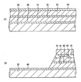
【解決手段】基板22に、n型クラッド層41ないしp型コンタクト層44を順次成長させ、p型コンタクト層44およびp型クラッド層43の上層部を選択的にエッチングして細い帯状の非対称なリッジ部を形成する。p型コンタクト層44ないしn型クラッド層41を選択的に除去することにより、基板22の(011)面側にAlGaInP系レーザ素子24を形成する。基板22に、n型クラッド層52ないしp型コンタクト層55を順次成長させたのち、これらを選択的に除去し、p型コンタクト層55およびp型クラッド層54の上層部に電流ブロック領域56を形成することにより、基板22の(0−1−1)面側にAlGaAsレーザ素子26を形成する。
【選択図】図3
Description
Claims (6)
- 共通基板の主面の隣接する位置に、主出射面が同一方向の少なくとも1組の発光素子を有する半導体発光装置の製造方法であって、
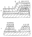
主出射面(01−1)側から見たその両側面が、結晶軸(100)方向に対して(0−1−1)面から(011)面に向かう方向に所定の角度(オフ角)で傾斜してなる共通基板に、第1のn型クラッド層,第1の活性層,第1のp型クラッド層および第1のp型コンタクト層を順次成長させる工程と、
前記第1のp型コンタクト層および前記第1のp型クラッド層の上層部を選択的にエッチングして細い帯状のリッジ部を形成すると共に、前記リッジ部を、主出射面側から見て、対向する2つの側面のうち左側が右側よりもなだらかな台形状の断面を有する非対称なリッジ部とする工程と、
前記第1のp型コンタクト層および前記第1のp型クラッド層の側面を覆う絶縁層を形成する工程と、
前記第1のp型コンタクト層,前記第1のp型クラッド層,前記第1の活性層および前記第1のn型クラッド層を選択的に除去することにより、前記共通基板の(011)面側に、主出射面側から見て、対向する2つの側面のうち左側が右側よりもなだらかな台形状の断面を有する第1の発光素子を形成する工程と、
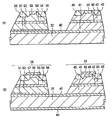
前記共通基板に、第2のn型クラッド層,第2の活性層,第2のp型クラッド層および第2のp型コンタクト層を順次成長させる工程と、
前記第2のp型コンタクト層,前記第2のp型クラッド層,前記第2の活性層および前記第2のn型クラッド層を選択的に除去する工程と、
前記第2のp型コンタクト層および前記第2のp型クラッド層の上層部に電流ブロック領域を形成することにより、前記共通基板の(0−1−1)面側に、前記第1の発光素子と対をなす第2の発光素子を形成する工程と
を含む半導体発光装置の製造方法。 - 前記第1の発光素子のリッジ部を、結晶方位に依存してエッチングレートに選択性のあるエッチャントを用いたウェットエッチングにより形成する
請求項1記載の半導体発光装置の製造方法。 - 前記第2の発光素子の電流ブロック領域を、イオン注入法により形成する
請求項2記載の半導体発光装置の製造方法。 - 前記基板のオフ角度は2度以上15度以下である
請求項1記載の半導体発光装置の製造方法。 - 前記基板はGaAs系の基板であり、前記第1の発光素子はAlGaInP系のレーザ素子、第2の発光素子はAlGaAs系のレーザ素子である
請求項1記載の半導体発光装置の製造方法。 - 前記第1の発光素子は650nm帯、前記第2の発光素子は750nm帯の波長のレーザ光をそれぞれ出射する
請求項5記載の半導体発光装置の製造方法。
Priority Applications (1)
| Application Number | Priority Date | Filing Date | Title |
|---|---|---|---|
| JP2009245841A JP5240156B2 (ja) | 2002-02-21 | 2009-10-26 | 半導体発光装置の製造方法 |
Applications Claiming Priority (3)
| Application Number | Priority Date | Filing Date | Title |
|---|---|---|---|
| JP2002044651 | 2002-02-21 | ||
| JP2002044651 | 2002-02-21 | ||
| JP2009245841A JP5240156B2 (ja) | 2002-02-21 | 2009-10-26 | 半導体発光装置の製造方法 |
Related Parent Applications (1)
| Application Number | Title | Priority Date | Filing Date |
|---|---|---|---|
| JP2003570434A Division JPWO2003071642A1 (ja) | 2002-02-21 | 2003-02-20 | 半導体発光装置およびそれを用いた光ディスク装置 |
Publications (2)
| Publication Number | Publication Date |
|---|---|
| JP2010021585A true JP2010021585A (ja) | 2010-01-28 |
| JP5240156B2 JP5240156B2 (ja) | 2013-07-17 |
Family
ID=27750560
Family Applications (2)
| Application Number | Title | Priority Date | Filing Date |
|---|---|---|---|
| JP2003570434A Pending JPWO2003071642A1 (ja) | 2002-02-21 | 2003-02-20 | 半導体発光装置およびそれを用いた光ディスク装置 |
| JP2009245841A Expired - Fee Related JP5240156B2 (ja) | 2002-02-21 | 2009-10-26 | 半導体発光装置の製造方法 |
Family Applications Before (1)
| Application Number | Title | Priority Date | Filing Date |
|---|---|---|---|
| JP2003570434A Pending JPWO2003071642A1 (ja) | 2002-02-21 | 2003-02-20 | 半導体発光装置およびそれを用いた光ディスク装置 |
Country Status (6)
| Country | Link |
|---|---|
| US (2) | US6995399B2 (ja) |
| JP (2) | JPWO2003071642A1 (ja) |
| KR (1) | KR100918328B1 (ja) |
| CN (1) | CN1264259C (ja) |
| TW (1) | TWI228338B (ja) |
| WO (1) | WO2003071642A1 (ja) |
Cited By (2)
| Publication number | Priority date | Publication date | Assignee | Title |
|---|---|---|---|---|
| JPWO2019021802A1 (ja) * | 2017-07-26 | 2020-05-28 | パナソニック株式会社 | 半導体レーザ素子及び半導体レーザ装置 |
| JPWO2019216364A1 (ja) * | 2018-05-09 | 2021-05-20 | 国立研究開発法人理化学研究所 | 光学装置及び光音響顕微鏡 |
Families Citing this family (12)
| Publication number | Priority date | Publication date | Assignee | Title |
|---|---|---|---|---|
| KR100918328B1 (ko) * | 2002-02-21 | 2009-09-22 | 소니 가부시끼 가이샤 | 반도체 발광 장치 및 그를 이용한 광디스크 장치 |
| JP2006120668A (ja) * | 2004-10-19 | 2006-05-11 | Mitsubishi Electric Corp | 半導体レーザ |
| JP2006313875A (ja) * | 2005-04-08 | 2006-11-16 | Mitsubishi Electric Corp | 半導体レーザ装置 |
| KR100848759B1 (ko) * | 2007-08-07 | 2008-07-25 | 김정수 | 복수개의 도파관이 형성된 반도체 레이저 다이오드 칩 |
| JP5347541B2 (ja) * | 2009-01-30 | 2013-11-20 | 三洋電機株式会社 | 半導体レーザ素子およびそれを備えた半導体レーザ装置 |
| JP2011049295A (ja) * | 2009-08-26 | 2011-03-10 | Toshiba Corp | 半導体レーザ装置 |
| JP5493624B2 (ja) * | 2009-09-15 | 2014-05-14 | ソニー株式会社 | 画像表示装置及び電子機器 |
| KR20140006485A (ko) * | 2012-07-05 | 2014-01-16 | 삼성전자주식회사 | 멀티셀 어레이를 갖는 반도체 발광장치 및 그 제조 방법 |
| KR20150101783A (ko) * | 2014-02-27 | 2015-09-04 | 서울바이오시스 주식회사 | 발광 다이오드 및 그 제조 방법 |
| JP6289640B2 (ja) * | 2014-07-25 | 2018-03-07 | 三菱電機株式会社 | 半導体レーザ装置 |
| US11398715B2 (en) * | 2018-02-26 | 2022-07-26 | Panasonic Holdings Corporation | Semiconductor light emitting device |
| KR102601950B1 (ko) * | 2018-11-16 | 2023-11-14 | 삼성전자주식회사 | Led 소자, led 소자의 제조 방법 및 led 소자를 포함하는 디스플레이 장치 |
Citations (2)
| Publication number | Priority date | Publication date | Assignee | Title |
|---|---|---|---|---|
| JP2000349387A (ja) * | 1999-06-02 | 2000-12-15 | Sony Corp | 半導体レーザ装置及びその作製方法 |
| JP2001144373A (ja) * | 1999-11-16 | 2001-05-25 | Matsushita Electronics Industry Corp | 半導体レーザ装置の製造方法 |
Family Cites Families (8)
| Publication number | Priority date | Publication date | Assignee | Title |
|---|---|---|---|---|
| JP3281805B2 (ja) * | 1996-06-28 | 2002-05-13 | 三洋電機株式会社 | 半導体レーザ装置 |
| JPH11186651A (ja) | 1997-12-19 | 1999-07-09 | Sony Corp | 集積型半導体発光装置 |
| JP4147602B2 (ja) * | 1998-02-02 | 2008-09-10 | ソニー株式会社 | 自励発振型半導体レーザ |
| JP2000244060A (ja) * | 1998-12-22 | 2000-09-08 | Sony Corp | 半導体発光装置およびその製造方法 |
| JP2000195827A (ja) * | 1998-12-25 | 2000-07-14 | Oki Electric Ind Co Ltd | Ledアレイチップおよびその製造方法ならびにダイシング装置 |
| US6813290B1 (en) * | 1999-11-25 | 2004-11-02 | Matsushita Electric Industrial Co., Ltd. | Semiconductor laser device and method for fabricating the same |
| JP2001244574A (ja) * | 1999-12-22 | 2001-09-07 | Asahi Glass Co Ltd | 2波長光源装置および光ヘッド装置 |
| KR100918328B1 (ko) * | 2002-02-21 | 2009-09-22 | 소니 가부시끼 가이샤 | 반도체 발광 장치 및 그를 이용한 광디스크 장치 |
-
2003
- 2003-02-20 KR KR1020037013697A patent/KR100918328B1/ko not_active IP Right Cessation
- 2003-02-20 WO PCT/JP2003/001833 patent/WO2003071642A1/ja active Application Filing
- 2003-02-20 US US10/473,688 patent/US6995399B2/en not_active Expired - Fee Related
- 2003-02-20 CN CNB038001373A patent/CN1264259C/zh not_active Expired - Fee Related
- 2003-02-20 JP JP2003570434A patent/JPWO2003071642A1/ja active Pending
- 2003-02-21 TW TW092103651A patent/TWI228338B/zh not_active IP Right Cessation
-
2005
- 2005-06-23 US US11/165,014 patent/US7141827B2/en not_active Expired - Fee Related
-
2009
- 2009-10-26 JP JP2009245841A patent/JP5240156B2/ja not_active Expired - Fee Related
Patent Citations (2)
| Publication number | Priority date | Publication date | Assignee | Title |
|---|---|---|---|---|
| JP2000349387A (ja) * | 1999-06-02 | 2000-12-15 | Sony Corp | 半導体レーザ装置及びその作製方法 |
| JP2001144373A (ja) * | 1999-11-16 | 2001-05-25 | Matsushita Electronics Industry Corp | 半導体レーザ装置の製造方法 |
Cited By (4)
| Publication number | Priority date | Publication date | Assignee | Title |
|---|---|---|---|---|
| JPWO2019021802A1 (ja) * | 2017-07-26 | 2020-05-28 | パナソニック株式会社 | 半導体レーザ素子及び半導体レーザ装置 |
| JPWO2019216364A1 (ja) * | 2018-05-09 | 2021-05-20 | 国立研究開発法人理化学研究所 | 光学装置及び光音響顕微鏡 |
| JP7291959B2 (ja) | 2018-05-09 | 2023-06-16 | 国立研究開発法人理化学研究所 | 光学装置及び光音響顕微鏡 |
| US11959882B2 (en) | 2018-05-09 | 2024-04-16 | Riken | Optical device and photoacoustic microscope |
Also Published As
| Publication number | Publication date |
|---|---|
| JP5240156B2 (ja) | 2013-07-17 |
| TW200405631A (en) | 2004-04-01 |
| KR100918328B1 (ko) | 2009-09-22 |
| US20040113157A1 (en) | 2004-06-17 |
| US6995399B2 (en) | 2006-02-07 |
| JPWO2003071642A1 (ja) | 2005-06-16 |
| WO2003071642A1 (en) | 2003-08-28 |
| KR20040078172A (ko) | 2004-09-09 |
| CN1498447A (zh) | 2004-05-19 |
| US7141827B2 (en) | 2006-11-28 |
| US20050258434A1 (en) | 2005-11-24 |
| CN1264259C (zh) | 2006-07-12 |
| TWI228338B (en) | 2005-02-21 |
Similar Documents
| Publication | Publication Date | Title |
|---|---|---|
| JP5240156B2 (ja) | 半導体発光装置の製造方法 | |
| JP3486900B2 (ja) | 発光装置およびそれを用いた光装置 | |
| JPH1146039A (ja) | 二波長単一構造集積縦型キャビティ表面放射レーザおよびその製造方法 | |
| JP2004193330A (ja) | モノリシック多波長レーザ素子とその製法 | |
| JP2000244060A (ja) | 半導体発光装置およびその製造方法 | |
| KR100782285B1 (ko) | 반도체 레이저 장치, 레이저 결합기, 데이터 재생 장치,데이터 기록 장치 및 반도체 레이저 장치의 제조 방법 | |
| US6930024B2 (en) | Semiconductor laser device and method for fabricating the same | |
| US6781944B1 (en) | Optical information processor with monolithically integrated light emitting device, light receiving devices and optics | |
| JP2002217499A (ja) | 半導体レーザ素子、その製造方法、およびそれを用いた光ピックアップ | |
| JP2003298193A (ja) | 発光装置およびそれを用いた光装置並びに発光装置の製造方法 | |
| JP2006080307A (ja) | 半導体レーザアレイ及びその製造方法、多波長半導体レーザ装置 | |
| JP3818815B2 (ja) | 半導体レーザ素子及びその製造方法 | |
| JP3493276B2 (ja) | 半導体レーザ装置及びその製造方法 | |
| KR100360143B1 (ko) | 반도체 레이저 소자 및 그의 제조방법 | |
| JP2000196203A (ja) | 半導体レ―ザ及びその製造方法 | |
| JP2000036639A (ja) | 半導体レーザ装置およびその製造方法、並びに、ピックアップ装置 | |
| JP2001250255A (ja) | 光学装置及び光ディスク装置 | |
| JP4821829B2 (ja) | 半導体発光装置の製造方法 | |
| JP4595929B2 (ja) | 発光装置の製造方法 | |
| JP2001244573A (ja) | 半導体発光装置の製造方法 | |
| JP2004047096A (ja) | 光学的記録再生装置用光学ヘッド | |
| JP2000187876A (ja) | 光学装置および光ディスク装置 | |
| WO2005015701A1 (ja) | 多ビームレーザを用いた光源 | |
| JP2004079168A (ja) | 光学的記録再生装置用光学ヘッド | |
| JP2005166817A (ja) | 半導体レーザ装置及びその製造方法 |
Legal Events
| Date | Code | Title | Description |
|---|---|---|---|
| A521 | Request for written amendment filed |
Free format text: JAPANESE INTERMEDIATE CODE: A523 Effective date: 20091027 |
|
| A621 | Written request for application examination |
Free format text: JAPANESE INTERMEDIATE CODE: A621 Effective date: 20091027 |
|
| A131 | Notification of reasons for refusal |
Free format text: JAPANESE INTERMEDIATE CODE: A131 Effective date: 20120905 |
|
| A521 | Request for written amendment filed |
Free format text: JAPANESE INTERMEDIATE CODE: A523 Effective date: 20121029 |
|
| TRDD | Decision of grant or rejection written | ||
| A01 | Written decision to grant a patent or to grant a registration (utility model) |
Free format text: JAPANESE INTERMEDIATE CODE: A01 Effective date: 20130305 |
|
| A61 | First payment of annual fees (during grant procedure) |
Free format text: JAPANESE INTERMEDIATE CODE: A61 Effective date: 20130318 |
|
| FPAY | Renewal fee payment (event date is renewal date of database) |
Free format text: PAYMENT UNTIL: 20160412 Year of fee payment: 3 |
|
| FPAY | Renewal fee payment (event date is renewal date of database) |
Free format text: PAYMENT UNTIL: 20160412 Year of fee payment: 3 |
|
| LAPS | Cancellation because of no payment of annual fees |