JP2010021585A - Method of manufacturing semiconductor light emitting device - Google Patents
Method of manufacturing semiconductor light emitting device Download PDFInfo
- Publication number
- JP2010021585A JP2010021585A JP2009245841A JP2009245841A JP2010021585A JP 2010021585 A JP2010021585 A JP 2010021585A JP 2009245841 A JP2009245841 A JP 2009245841A JP 2009245841 A JP2009245841 A JP 2009245841A JP 2010021585 A JP2010021585 A JP 2010021585A
- Authority
- JP
- Japan
- Prior art keywords
- light emitting
- layer
- substrate
- laser
- cladding layer
- Prior art date
- Legal status (The legal status is an assumption and is not a legal conclusion. Google has not performed a legal analysis and makes no representation as to the accuracy of the status listed.)
- Granted
Links
Images


Classifications
-
- G—PHYSICS
- G11—INFORMATION STORAGE
- G11B—INFORMATION STORAGE BASED ON RELATIVE MOVEMENT BETWEEN RECORD CARRIER AND TRANSDUCER
- G11B7/00—Recording or reproducing by optical means, e.g. recording using a thermal beam of optical radiation by modifying optical properties or the physical structure, reproducing using an optical beam at lower power by sensing optical properties; Record carriers therefor
- G11B7/12—Heads, e.g. forming of the optical beam spot or modulation of the optical beam
- G11B7/125—Optical beam sources therefor, e.g. laser control circuitry specially adapted for optical storage devices; Modulators, e.g. means for controlling the size or intensity of optical spots or optical traces
- G11B7/126—Circuits, methods or arrangements for laser control or stabilisation
-
- B—PERFORMING OPERATIONS; TRANSPORTING
- B82—NANOTECHNOLOGY
- B82Y—SPECIFIC USES OR APPLICATIONS OF NANOSTRUCTURES; MEASUREMENT OR ANALYSIS OF NANOSTRUCTURES; MANUFACTURE OR TREATMENT OF NANOSTRUCTURES
- B82Y20/00—Nanooptics, e.g. quantum optics or photonic crystals
-
- G—PHYSICS
- G11—INFORMATION STORAGE
- G11B—INFORMATION STORAGE BASED ON RELATIVE MOVEMENT BETWEEN RECORD CARRIER AND TRANSDUCER
- G11B7/00—Recording or reproducing by optical means, e.g. recording using a thermal beam of optical radiation by modifying optical properties or the physical structure, reproducing using an optical beam at lower power by sensing optical properties; Record carriers therefor
- G11B7/12—Heads, e.g. forming of the optical beam spot or modulation of the optical beam
- G11B7/125—Optical beam sources therefor, e.g. laser control circuitry specially adapted for optical storage devices; Modulators, e.g. means for controlling the size or intensity of optical spots or optical traces
- G11B7/127—Lasers; Multiple laser arrays
- G11B7/1275—Two or more lasers having different wavelengths
-
- H—ELECTRICITY
- H01—ELECTRIC ELEMENTS
- H01S—DEVICES USING THE PROCESS OF LIGHT AMPLIFICATION BY STIMULATED EMISSION OF RADIATION [LASER] TO AMPLIFY OR GENERATE LIGHT; DEVICES USING STIMULATED EMISSION OF ELECTROMAGNETIC RADIATION IN WAVE RANGES OTHER THAN OPTICAL
- H01S5/00—Semiconductor lasers
- H01S5/02—Structural details or components not essential to laser action
- H01S5/026—Monolithically integrated components, e.g. waveguides, monitoring photo-detectors, drivers
-
- H—ELECTRICITY
- H01—ELECTRIC ELEMENTS
- H01S—DEVICES USING THE PROCESS OF LIGHT AMPLIFICATION BY STIMULATED EMISSION OF RADIATION [LASER] TO AMPLIFY OR GENERATE LIGHT; DEVICES USING STIMULATED EMISSION OF ELECTROMAGNETIC RADIATION IN WAVE RANGES OTHER THAN OPTICAL
- H01S5/00—Semiconductor lasers
- H01S5/20—Structure or shape of the semiconductor body to guide the optical wave ; Confining structures perpendicular to the optical axis, e.g. index or gain guiding, stripe geometry, broad area lasers, gain tailoring, transverse or lateral reflectors, special cladding structures, MQW barrier reflection layers
- H01S5/22—Structure or shape of the semiconductor body to guide the optical wave ; Confining structures perpendicular to the optical axis, e.g. index or gain guiding, stripe geometry, broad area lasers, gain tailoring, transverse or lateral reflectors, special cladding structures, MQW barrier reflection layers having a ridge or stripe structure
-
- H—ELECTRICITY
- H01—ELECTRIC ELEMENTS
- H01S—DEVICES USING THE PROCESS OF LIGHT AMPLIFICATION BY STIMULATED EMISSION OF RADIATION [LASER] TO AMPLIFY OR GENERATE LIGHT; DEVICES USING STIMULATED EMISSION OF ELECTROMAGNETIC RADIATION IN WAVE RANGES OTHER THAN OPTICAL
- H01S5/00—Semiconductor lasers
- H01S5/30—Structure or shape of the active region; Materials used for the active region
- H01S5/32—Structure or shape of the active region; Materials used for the active region comprising PN junctions, e.g. hetero- or double- heterostructures
- H01S5/323—Structure or shape of the active region; Materials used for the active region comprising PN junctions, e.g. hetero- or double- heterostructures in AIIIBV compounds, e.g. AlGaAs-laser, InP-based laser
-
- H—ELECTRICITY
- H01—ELECTRIC ELEMENTS
- H01S—DEVICES USING THE PROCESS OF LIGHT AMPLIFICATION BY STIMULATED EMISSION OF RADIATION [LASER] TO AMPLIFY OR GENERATE LIGHT; DEVICES USING STIMULATED EMISSION OF ELECTROMAGNETIC RADIATION IN WAVE RANGES OTHER THAN OPTICAL
- H01S5/00—Semiconductor lasers
- H01S5/20—Structure or shape of the semiconductor body to guide the optical wave ; Confining structures perpendicular to the optical axis, e.g. index or gain guiding, stripe geometry, broad area lasers, gain tailoring, transverse or lateral reflectors, special cladding structures, MQW barrier reflection layers
- H01S5/22—Structure or shape of the semiconductor body to guide the optical wave ; Confining structures perpendicular to the optical axis, e.g. index or gain guiding, stripe geometry, broad area lasers, gain tailoring, transverse or lateral reflectors, special cladding structures, MQW barrier reflection layers having a ridge or stripe structure
- H01S5/2201—Structure or shape of the semiconductor body to guide the optical wave ; Confining structures perpendicular to the optical axis, e.g. index or gain guiding, stripe geometry, broad area lasers, gain tailoring, transverse or lateral reflectors, special cladding structures, MQW barrier reflection layers having a ridge or stripe structure in a specific crystallographic orientation
-
- H—ELECTRICITY
- H01—ELECTRIC ELEMENTS
- H01S—DEVICES USING THE PROCESS OF LIGHT AMPLIFICATION BY STIMULATED EMISSION OF RADIATION [LASER] TO AMPLIFY OR GENERATE LIGHT; DEVICES USING STIMULATED EMISSION OF ELECTROMAGNETIC RADIATION IN WAVE RANGES OTHER THAN OPTICAL
- H01S5/00—Semiconductor lasers
- H01S5/30—Structure or shape of the active region; Materials used for the active region
- H01S5/34—Structure or shape of the active region; Materials used for the active region comprising quantum well or superlattice structures, e.g. single quantum well [SQW] lasers, multiple quantum well [MQW] lasers or graded index separate confinement heterostructure [GRINSCH] lasers
- H01S5/343—Structure or shape of the active region; Materials used for the active region comprising quantum well or superlattice structures, e.g. single quantum well [SQW] lasers, multiple quantum well [MQW] lasers or graded index separate confinement heterostructure [GRINSCH] lasers in AIIIBV compounds, e.g. AlGaAs-laser, InP-based laser
- H01S5/34313—Structure or shape of the active region; Materials used for the active region comprising quantum well or superlattice structures, e.g. single quantum well [SQW] lasers, multiple quantum well [MQW] lasers or graded index separate confinement heterostructure [GRINSCH] lasers in AIIIBV compounds, e.g. AlGaAs-laser, InP-based laser with a well layer having only As as V-compound, e.g. AlGaAs, InGaAs
-
- H—ELECTRICITY
- H01—ELECTRIC ELEMENTS
- H01S—DEVICES USING THE PROCESS OF LIGHT AMPLIFICATION BY STIMULATED EMISSION OF RADIATION [LASER] TO AMPLIFY OR GENERATE LIGHT; DEVICES USING STIMULATED EMISSION OF ELECTROMAGNETIC RADIATION IN WAVE RANGES OTHER THAN OPTICAL
- H01S5/00—Semiconductor lasers
- H01S5/30—Structure or shape of the active region; Materials used for the active region
- H01S5/34—Structure or shape of the active region; Materials used for the active region comprising quantum well or superlattice structures, e.g. single quantum well [SQW] lasers, multiple quantum well [MQW] lasers or graded index separate confinement heterostructure [GRINSCH] lasers
- H01S5/343—Structure or shape of the active region; Materials used for the active region comprising quantum well or superlattice structures, e.g. single quantum well [SQW] lasers, multiple quantum well [MQW] lasers or graded index separate confinement heterostructure [GRINSCH] lasers in AIIIBV compounds, e.g. AlGaAs-laser, InP-based laser
- H01S5/34326—Structure or shape of the active region; Materials used for the active region comprising quantum well or superlattice structures, e.g. single quantum well [SQW] lasers, multiple quantum well [MQW] lasers or graded index separate confinement heterostructure [GRINSCH] lasers in AIIIBV compounds, e.g. AlGaAs-laser, InP-based laser with a well layer based on InGa(Al)P, e.g. red laser
-
- H—ELECTRICITY
- H01—ELECTRIC ELEMENTS
- H01S—DEVICES USING THE PROCESS OF LIGHT AMPLIFICATION BY STIMULATED EMISSION OF RADIATION [LASER] TO AMPLIFY OR GENERATE LIGHT; DEVICES USING STIMULATED EMISSION OF ELECTROMAGNETIC RADIATION IN WAVE RANGES OTHER THAN OPTICAL
- H01S5/00—Semiconductor lasers
- H01S5/40—Arrangement of two or more semiconductor lasers, not provided for in groups H01S5/02 - H01S5/30
- H01S5/4025—Array arrangements, e.g. constituted by discrete laser diodes or laser bar
- H01S5/4031—Edge-emitting structures
- H01S5/4056—Edge-emitting structures emitting light in more than one direction
-
- H—ELECTRICITY
- H01—ELECTRIC ELEMENTS
- H01S—DEVICES USING THE PROCESS OF LIGHT AMPLIFICATION BY STIMULATED EMISSION OF RADIATION [LASER] TO AMPLIFY OR GENERATE LIGHT; DEVICES USING STIMULATED EMISSION OF ELECTROMAGNETIC RADIATION IN WAVE RANGES OTHER THAN OPTICAL
- H01S5/00—Semiconductor lasers
- H01S5/40—Arrangement of two or more semiconductor lasers, not provided for in groups H01S5/02 - H01S5/30
- H01S5/4025—Array arrangements, e.g. constituted by discrete laser diodes or laser bar
- H01S5/4087—Array arrangements, e.g. constituted by discrete laser diodes or laser bar emitting more than one wavelength
Abstract
Description
本発明は、1チップに発光波長の異なる複数の発光素子が作り込まれた所謂モノシリック型の半導体発光装置およびこれを用いた光ディスク装置に係り、特に、発光素子としてAlGaInP系およびAlGaAs系の素子を共通基板上に有する半導体発光装置および光ディスク装置に関する。 The present invention relates to a so-called monolithic semiconductor light-emitting device in which a plurality of light-emitting elements having different emission wavelengths are formed in one chip and an optical disk device using the same, and in particular, AlGaInP-based and AlGaAs-based devices are used as the light-emitting elements. The present invention relates to a semiconductor light emitting device and an optical disk device which are provided on a common substrate.
近年、半導体発光装置の分野においては、共通基板上に発光波長が異なる複数の発光素子を有する半導体レーザ(LD;laser diode )(多波長レーザという。)の開発が活発になされている。 In recent years, in the field of semiconductor light emitting devices, development of semiconductor lasers (LD; laser diode) (referred to as multi-wavelength lasers) having a plurality of light emitting elements having different emission wavelengths on a common substrate has been actively conducted.
これらの多波長レーザは、例えば光ディスク装置の光源として用いられる。現在、一般に光ディスク装置では、780nm帯の半導体レーザ光がCD(Compact Disk)の再生に用いられると共に、CD−R(CD recordable ),CD−RW(CD Rewritable )あるいはMD(Mini Disk )などの記録可能な光ディスクの記録・再生に用いられている。また、650nm帯の半導体レーザ光がDVD(Digital Versatile Disk)の記録・再生に用いられている。従って、上述したような多波長レーザを光ディスク装置に搭載することにより、既存の複数種類の光ディスクのいずれに関しても、記録または再生が可能となる。 These multi-wavelength lasers are used, for example, as a light source of an optical disc apparatus. Currently, in an optical disk apparatus, a semiconductor laser beam of 780 nm band is generally used for reproducing a CD (Compact Disk) and recording such as a CD-R (CD recordable), a CD-RW (CD Rewritable), or an MD (Mini Disk). It is used for recording and playback of possible optical discs. Further, a semiconductor laser beam of 650 nm band is used for recording / reproducing of a DVD (Digital Versatile Disk). Accordingly, by mounting the multi-wavelength laser as described above on the optical disc apparatus, it is possible to record or reproduce any of a plurality of existing types of optical discs.
このような多波長レーザの一例として、1チップに発光波長の異なる2つの半導体レーザが作り込まれた所謂モノシリック2波長半導体レーザが提案されている。このモノシリックレーザをDVDおよびCDの再生/記録処理の共通光源として用いることにより、光学ピックアップの小型化と光学系の調整の簡略化を図ることが可能になる。 As an example of such a multi-wavelength laser, a so-called monolithic two-wavelength semiconductor laser in which two semiconductor lasers having different emission wavelengths are formed in one chip has been proposed. By using this monolithic laser as a common light source for DVD / CD reproduction / recording processing, it is possible to reduce the size of the optical pickup and simplify the adjustment of the optical system.
この種の2波長半導体レーザとしては、DVD用の光源としてのAlGaInP系の赤色半導体レーザ素子(以下、AlGaInP系レーザ素子という)と、CD用の光源としてのAlGaAsの赤色半導体レーザ素子(以下、AlGaAs系レーザ素子という)とを備えたものが挙げられる。 As this type of two-wavelength semiconductor laser, an AlGaInP-based red semiconductor laser element (hereinafter referred to as an AlGaInP-based laser element) as a light source for DVD and an AlGaAs red semiconductor laser element (hereinafter referred to as AlGaAs as a light source for CD). System laser element).
図7(A),図7(B)は、この2波長半導体レーザの具体的な構成の一例を表すもので、図7(A)は平面構成、図7(B)は図7(A)の矢視II−II線に沿った断面構成であり、レーザ光の主出射面側から見た図である。2波長半導体レーザ10は、GaAsからなる共通の基板11上にAlGaInP系レーザ素子12とAlGaAs系レーザ素子13とを備えている。基板11は所定の角度(オフ角)で傾斜した所謂オフ基板(off 基板)であり、ここでは主出射面(011)11cから見て、結晶面(100)に対して反時計廻り方向、すなわち(011)面11aから(011)面11bに向かって傾斜している。
FIGS. 7A and 7B show an example of a specific configuration of the two-wavelength semiconductor laser. FIG. 7A is a plan configuration, and FIG. 7B is FIG. It is the cross-sectional structure along arrow II-II line | wire, and is the figure seen from the main output surface side of the laser beam. The two-
このようにオフ基板を用いるのは、基板から成長するレーザ素子12,13に対して自然超格子が形成されるのを抑制し、発振波長の短波長化を図るためである。
The reason why the off-substrate is used is to suppress the formation of a natural superlattice for the
AlGaInP系レーザ素子12は、発振波長650nm帯の赤色発光素子であり、基板11上に順次成膜された、AlGaInP下部クラッド層、活性層、AlGaInP上部クラッド層、GaInP層およびGaAsコンタクト層等により構成され、その上部部分は、両側に絶縁層からなる電流ブロック領域17が形成されたエアエッジ型レーザストライプ14となっている。一方、AlGaAs系レーザ素子13は、発振波長780nm帯の赤色発光素子であり、基板11上に順次成膜された、AlGaAs下部クラッド層、活性層、AlGaAs上部クラッド層、GaAsコンタクト層等を備え、その上部部分は、両側にB+ イオンのイオン注入層からなる電流ブロック領域16が形成された埋め込み型のレーザストライプ15となっている。
The AlGaInP-based
AlGaInP系レーザ素子12およびAlGaAs系レーザ素子13は、各々のレーザストライプ14,15が互に平行になるように配置されると共に、レーザ光の主出射面(011)11c側から見て、AlGaInP系レーザ素子12は基板中心線より(011)面11a側に、AlGaAs系レーザ素子13は基板中心線より(011)面11b側に配置されており、レーザストライプ14,15の中心線間隔Sは120μmとなっている。
The AlGaInP
上述の2波長半導体レーザでは、図8からも明らかなように、AlGaInP系レーザ素子12の光軸L1 と、AlGaAs系レーザ素子13の光軸L2 とは主出射面側から見て間隔S分だけずれている。
The two-wavelength semiconductor laser described above, as is apparent from FIG. 8, the optical axis L 1 of the AlGaInP-based
したがって、この2波長半導体レーザを、DVDおよびCDの再生/記録装置の共通光源として用いる場合には、DVDまたはCDの読み出しまたは書き換えに際し、AlGaInP系レーザ素子とAlGaAs系レーザ素子との間で共通光学系の切り換え、すなわち各々の光軸を共通光学系に対して整合させることが必要になる。 Therefore, when this two-wavelength semiconductor laser is used as a common light source for a DVD / CD reproducing / recording device, a common optical element is used between the AlGaInP laser element and the AlGaAs laser element when reading or rewriting the DVD or CD. It is necessary to switch the system, that is, to align each optical axis with the common optical system.
このようにAlGaInP系レーザ素子またはAlGaAs系レーザ素子の光軸を共通光学系に対して整合させるためには、共通光学系のレンズを相対的に移動させる必要があるが、その移動量は、装置全体の小型化のためには最小限にすることが望ましい。このようなことから従来の2波長半導体レーザでは、AlGaInP系レーザ素子12およびAlGaAs系レーザ素子13の互いのレーザ光の主出射位置が近接するようにレーザストライプ14,15が配置されている。
Thus, in order to align the optical axis of the AlGaInP laser element or AlGaAs laser element with the common optical system, it is necessary to relatively move the lens of the common optical system. It is desirable to minimize it for the entire size reduction. For this reason, in the conventional two-wavelength semiconductor laser, the
しかしながら、従来の2波長半導体レーザでは、レーザストライプ14,15が近接するように2つの素子を配置しているものの、ある程度の分離領域が必要であり、2つの素子間の間隔Sを短くするには限界があった。
However, in the conventional two-wavelength semiconductor laser, although two elements are arranged so that the
また、理由は後述するが、2つの素子を極力近接させたとしても、図8にも示したようにAlGaInP系レーザ素子12の光軸L1 がレーザストライプ14の中心軸14aから外側にずれ、光軸L1 と光軸L2 との間が離れてしまい、その結果、共通光学系のレンズシフト量が素子間の距離Sよりも大きくなるという問題があった。
Although the reason will be described later, even if the two elements are made as close as possible, the optical axis L 1 of the AlGaInP-based
本発明はかかる問題点に鑑みてなされたもので、第1の目的は、2つの発光素子の光軸間の間隔をより短くし、光ディスク装置に適用した場合の共通光学系のレンズシフト量を最小限にすることができ、光ディスク装置の小型化を図ることができる半導体発光装置を提供することにある。 The present invention has been made in view of such problems, and a first object is to reduce the distance between the optical axes of the two light emitting elements and to reduce the lens shift amount of the common optical system when applied to an optical disc apparatus. It is an object of the present invention to provide a semiconductor light emitting device that can be minimized and can reduce the size of an optical disk device.
本発明の第2の目的は、本発明の半導体発光装置を用いて、共通光学系のレンズシフト量を最小限にすることができ、それによって小型化を図ることができる光ディスク装置を提供することにある。 A second object of the present invention is to provide an optical disc apparatus that can minimize the lens shift amount of the common optical system by using the semiconductor light emitting device of the present invention, and thereby can be miniaturized. It is in.
本発明による半導体発光装置は、共通基板の主面の隣接する位置に、主出射面が同一方向の少なくとも1組の発光素子を有するものであって、主出射面側から見て、側面が結晶軸方向に対して時計廻り方向に所定の角度(オフ角)で傾斜してなる基板と、主出射面側から見て、対向する2つの側面のうち左側が右側よりもなだらかな台形状の断面を有する第1の発光素子と、この第1の発光素子と対をなすと共に、主出射面側からみて、前記第1の発光素子の左側に形成された第2の発光素子とを備えたものである。 The semiconductor light emitting device according to the present invention has at least one set of light emitting elements whose main emission surfaces are in the same direction at positions adjacent to the main surface of the common substrate, and the side surfaces are crystallized when viewed from the main emission surface side. A substrate that is inclined at a predetermined angle (off angle) in the clockwise direction with respect to the axial direction, and a trapezoidal cross section in which the left side of the two opposing side surfaces is gentler than the right side when viewed from the main emission surface side. A first light emitting element having a first light emitting element, and a second light emitting element formed on the left side of the first light emitting element as viewed from the main emission surface side It is.
このような構成を有すると、第1の発光素子および第2の発光素子をともに互いに平行な帯状形状とした場合、素子材料の選択によって、第2の発光素子は帯状形状の中心軸と光軸方向が一致するのに対し、第1の発光素子は、その光軸が帯状形状の中心軸と一致若しくは第2の発光素子の光軸側に接近する。 With such a configuration, when both the first light-emitting element and the second light-emitting element have a strip shape parallel to each other, the second light-emitting element has a central axis and an optical axis depending on the selection of the element material. Whereas the directions coincide, the optical axis of the first light emitting element coincides with the central axis of the band shape or approaches the optical axis side of the second light emitting element.
具体的には以下の構成とすることが望ましい。 Specifically, the following configuration is desirable.
すなわち、第1の発光素子および第2の発光素子の主出射面は(011)面であると共に、基板は、主出射面側から見たその両側面が、結晶軸(100)に対して(011)面から(011)面に向かう方向に傾斜してなり、第1の発光素子は(011)面側、第2の発光素子は(011)面側にそれぞれ配置されている。また、基板はGaAs系でそのオフ角度は2度以上15度以下であり、第1の発光素子はAlGaInP系のレーザ素子、第2の発光素子はAlGaAs系のレーザ素子であることが好ましい。 That is, the main emission surface of the first light-emitting element and the second light-emitting element is the (011) plane, and the substrate has both side surfaces viewed from the main emission surface side with respect to the crystal axis (100) ( The first light emitting element is disposed on the (011) plane side, and the second light emitting element is disposed on the (011) plane side. Further, it is preferable that the substrate is a GaAs type and the off angle is 2 degrees or more and 15 degrees or less, the first light emitting element is an AlGaInP type laser element, and the second light emitting element is an AlGaAs type laser element.
本発明による光ディスク装置は、本発明の半導体発光装置を光源とし、複数種類の光ディスクに対して情報の記録または再生のうちの少なくとも一方を行うものであり、光ディスクに対する情報の読み出しまたは書き込みを行う際に、第1の発光素子と第2の発光素子の光軸同士が平行若しくは接近しているため、従来に比べて、少ないレンズシフト量をもって、例えばDVDからCD、あるいはCDからDVDへの切り換えが行われる。 An optical disc apparatus according to the present invention uses the semiconductor light emitting device of the present invention as a light source, and performs at least one of recording and reproduction of information with respect to a plurality of types of optical discs. In addition, since the optical axes of the first light-emitting element and the second light-emitting element are parallel or close to each other, switching from, for example, a DVD to a CD or a CD to a DVD can be performed with a small lens shift amount as compared with the prior art. Done.
以上説明したように本発明の半導体発光装置によれば、主出射面側から見て、側面が時計廻り方向に所定の角度(オフ角)で傾斜してなる基板の主面に、断面が台形(リッジ)状の第1の発光素子を、主出射面側から見て、対向する2つの側面のうち左側が右側よりもなだらかになるように形成すると共に、第2の発光素子を主出射面側から見て、第1の発光素子の左側に形成するようにしたので、従来のものに比べて第1の発光素子の光軸が第2の発光素子の光軸側に接近する。 As described above, according to the semiconductor light emitting device of the present invention, the cross section is trapezoidal on the main surface of the substrate whose side surface is inclined at a predetermined angle (off angle) in the clockwise direction when viewed from the main emission surface side. The (ridge) -shaped first light emitting element is formed so that the left side of the two opposing side surfaces becomes gentler than the right side when viewed from the main emitting surface side, and the second light emitting element is formed on the main emitting surface. Since it is formed on the left side of the first light emitting element when viewed from the side, the optical axis of the first light emitting element is closer to the optical axis side of the second light emitting element than the conventional one.
したがって、この半導体発光装置を光ディスク装置の光源とすることにより、光ディスクに対する情報の読み出しまたは書き込みを行う際に、わずかなレンズシフト量をもって、例えばDVDからCD、あるいはCDからDVDへの切り換えを行うことができる。よって、レンズシフト量が従来のモノシリック2波長半導体レーザに比べて著しく小さくなり、これにより光学ピックアップの光学系の調整が容易になり、製造歩留りが向上する。また、レンズシフト量を小さくできることからレンズシフトに伴う光学収差を低減でき、DVD,CD等のディスクDからの信号のSN比(ジッター)を高く確保でき、安定した性能で光学ピックアップによる読み取りおよび書き込みを行うことが可能になる。 Therefore, by using this semiconductor light-emitting device as a light source of an optical disk device, when reading or writing information on the optical disk, for example, switching from DVD to CD or from CD to DVD is performed with a slight lens shift amount. Can do. Therefore, the lens shift amount is remarkably small as compared with the conventional monolithic two-wavelength semiconductor laser, which facilitates the adjustment of the optical system of the optical pickup and improves the manufacturing yield. In addition, since the lens shift amount can be reduced, optical aberrations associated with the lens shift can be reduced, a high signal-to-noise ratio (jitter) of the signal from the disk D such as a DVD or CD can be secured, and reading and writing with an optical pickup with stable performance. It becomes possible to do.
以下、本発明の実施の形態について、図面を参照して詳細に説明する。 Hereinafter, embodiments of the present invention will be described in detail with reference to the drawings.
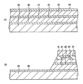
図1(A)および図1(B)は、本発明の一実施の形態に係る2波長半導体レーザ20の構成を表すもので、図1(A)は平面状態、図1(B)は図1(A)の矢視I−I線に沿った断面構成であり、レーザ光の主出射面側から見た図である。
1A and 1B illustrate a configuration of a two-
この2波長半導体レーザ20は、GaAsからなる共通の基板22の主面に、AlGaInP系レーザ素子24およびAlGaAs系レーザ素子26を備えている。基板22は両側面が結晶軸方向に対して所定の角度(オフ角θoff )で傾斜したオフ基板(off 基板)であり、ここでは、紙面手前側から見て時計廻り方向、すなわち(011)面22aから(011)面22bに向かって(100)面に対して2度以上15度以下の範囲の角度(θoff )をもって傾斜している。2つのレーザ光の主出射面は、紙面の手前側、すなわち(011)面22cである。
The two-
この基板22上に後述の成長法により形成されるAlGaInP系レーザ素子24は断面が非対称のリッジ(台形)形状となり、主出射面側から見て、対向する2つの側面のうち左側の面24aは右側の面24bよりもなだらかになる。AlGaAs系レーザ素子26も同様に、主出射面側から見て、対向する2つの側面のうち左側の面26aが右側の面26bよりもなだらかになる。
An AlGaInP-based
AlGaInP系レーザ素子24は、例えば発振波長650nm帯の赤色発光素子であり、基板22上に順次成膜された、GaInPバッファ層、AlGaInP下部クラッド層、活性層、AlGaInP上部クラッド層、GaInP層およびGaAsコンタクト層等により構成され、その上部部分は両側に電流ブロック領域45が形成されたエアエッジ型のレーザストライプ28となっている。
The AlGaInP-based
一方、AlGaAs系レーザ素子26は、例えば発振波長780nm帯の赤色発光素子であり、基板22上に順次成膜された、GaAsバッファ層、AlGaAs下部クラッド層、活性層、AlGaAs上部クラッド層およびGaAsコンタクト層等により構成され、その上部部分は両側にB+ イオンのイオン注入層からなる電流ブロック領域56が形成された埋め込み型のレーザストライプ30となっている。
On the other hand, the
AlGaInP系レーザ素子24およびAlGaAs系レーザ素子26は、各々のストライプ28,30が互に平行になるように配置されると共に、レーザ光の主出射面(011)面22c側から見て、AlGaInP系レーザ素子24は基板中心線より(011)面22b側に、AlGaAs系レーザ素子26は基板中心線より(011)面22a側に配置されており、ストライプ28,30の中心線間隔Sは120μmとなっている。
The AlGaInP-based
図7(B)でも説明したように、従来の2波長半導体レーザ10においては、レーザ光の主出射面(011)11c側から見て、基板11の傾斜方向は半時計廻り方向であり、かつ、AlGaInP系レーザ素子12は基板中心線より(011)面11a側に、AlGaAs系レーザ素子13は基板中心線より(011)面11b側に配置されている。
7B, in the conventional two-
これに対して、本実施の形態の2波長半導体レーザ20は、基板22の傾斜の向きが逆であり、レーザ光の主出射面(011)面22c側から見て、AlGaInP系レーザ素子24を基板中心線より(011)面22b側(右側)に、また、AlGaAs系レーザ素子26を基板中心線より(011)面22a側(左側)に配置するようにしたものである。ここで、レーザ光の主出射面から見た、AlGaInP系レーザ素子24のAlGaAs系レーザ素子26側、すなわち左側の傾斜面24aは右側の傾斜面24bよりもなだらかになっている。
On the other hand, in the two-
本発明者らは、DVDからCD、あるいはCDからDVDに切り換える際のレンズシフト量を小さくする研究の過程で、従来のモノシリック2波長半導体レーザでは、図8にも示したように、AlGaInP系レーザ素子12の光軸L1 がレーザ光の主出射方向に向かって、AlGaAs系レーザ素子13の光軸L2 から離間するように、つまり離れ目になっているために、レンズ移動量が大きくなっていることを見いだした。そして、広がりの角度θが大きい場合には、レンズシフト量による調整範囲を超えるために、光ピックアップの性能不良を生ずることもあることが判明した。
In the course of research to reduce the lens shift amount when switching from DVD to CD or from CD to DVD, the present inventors have used an AlGaInP laser as shown in FIG. Since the optical axis L 1 of the
AlGaInP系レーザ素子12の光軸L1 が離れ目になる理由は以下のように考えられる。すなわち、前述のように発振波長の短波長化を図るためにオフ基板を使用したとき、ウェットエッチングによりリッジ部を形成すると、リッジ部が非対称になる。これはエッチングを、結晶方位に依存してエッチングレートに選択性のあるエッチャントを用いるためである。このようにリッジ部の側壁の傾斜角度が非対称になることによって、傾斜のなだらかな方(図7(B)では右側)で光の閉じ込め効果が弱くなり光分布が非対称になる結果、2つのレーザの光軸が離れ目になる。
The reason why the optical axis L 1 of the AlGaInP-based
そこで、本発明者らは、上記オフ基板とは逆方向に傾斜したオフ基板(逆オフ基板)を用いると、リッジ部の側壁の傾斜具合が従来と左右が逆になり光閉じ込めの非対称性も逆になって2つの光軸が接近すると考え、種々の実験を行った。実験の結果、2度以上15度以下の範囲の傾斜角度(オフ角度)を有するオフ基板上に、上述のような特定の位置関係をもって2つレーザ素子を配置することにより、2つのレーザ素子の光軸同士を互いに平行にし、更には接近させることができることを見いだした。 Therefore, the present inventors use an off-substrate (reverse off-substrate) inclined in the opposite direction to the above-mentioned off-substrate, and the inclination of the side wall of the ridge portion is reversed from the left and right, and the asymmetry of light confinement is also achieved. On the contrary, it was considered that the two optical axes approached, and various experiments were conducted. As a result of the experiment, two laser elements are disposed on an off-substrate having an inclination angle (off angle) in the range of 2 degrees to 15 degrees with the specific positional relationship as described above. It has been found that the optical axes can be made parallel to each other and even closer.
オフ角度(θoff )が2度未満になると自然超格子発生の抑制効果がでないために、発振波長が所望の波長よりも大きくなってしまい、また、15度よりも大きくなると、以下の2つの問題が発生する。第1に、オフ角度が15度よりも大きくなると、リッジ形状の非対称性が強まり、逆オフ基板を用いた場合の2つのレーザの光軸の接近度合いが強まり過ぎる。 When the off-angle (θoff) is less than 2 degrees, the effect of suppressing the generation of natural superlattice is not achieved, so that the oscillation wavelength becomes larger than the desired wavelength, and when it exceeds 15 degrees, the following two problems Will occur. First, when the off angle is larger than 15 degrees, the asymmetry of the ridge shape is strengthened, and the degree of approach between the optical axes of the two lasers when the reverse off substrate is used becomes too strong.
第2に、オフ角度が15度よりも大きくなると、チップ化する際に劈開させたときに、チップの断面形状が平行四辺形となる度合が強まり、チップマウントやワイヤボンドの組立工程において支障をきたすことになる。また、オフ角度が15度よりも大きくなっても、短波長化の効果は変わらず、10度の場合と同程度である。 Second, if the off-angle is larger than 15 degrees, when the chip is cleaved, the degree of cross-sectional shape of the chip becomes a parallelogram is increased, which hinders the assembly process of chip mount and wire bond. Will come. Also, even if the off-angle is larger than 15 degrees, the effect of shortening the wavelength is not changed, which is about the same as the case of 10 degrees.
本実施の形態の2波長半導体レーザ20では、上述の構成によって、図2に示したように、AlGaInP系レーザ素子24の光軸L1 を、AlGaAs系レーザ素子26の光軸L2 に対して平行、更には0.5度(=θ)程度の角度で接近させることができる。ここで、θは、AlGaInP系レーザ素子24におけるレーザストライプ28の中心軸28aと光軸L1 との間のなす角度である。なお、AlGaAs系レーザ素子26の光軸L2 はレーザストライプ30の中心軸30aとほぼ一致する。
2 the
このようにAlGaInP系レーザ素子24およびAlGaAs系レーザ素子26の光軸L1 ,L2 同士が平行になる若しくは接近することから、後述のように、読み出しまたは書き込みを行う際に、DVDからCD、あるいはCDからDVDに切り換えるときのレンズシフト量を従来のモノシリック2波長半導体レーザ10に比べて著しく小さくすることができる。
As described above, since the optical axes L 1 and L 2 of the
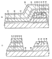
次に、上記2波長半導体レーザ20の製造方法について説明する。
Next, a method for manufacturing the two-
まず、図3(A)に示したように、例えば、厚さ350μm程度のn型GaAsよりなる基板22(オフ基板)を用意し、この基板22の表面にMOCVD法により、n型InGaP混晶よりなるバッファ層40,n型AlGaInP混晶よりなるn型クラッド層41,Alx Gay In1-x-y P(但し、x≧0かつy≧0)混晶よりなる活性層42,p型AlGaInP混晶よりなるp型クラッド層43およびp型GaAsよりなるp型コンタクト層44を順次成長させる。
First, as shown in FIG. 3A, for example, a substrate 22 (off substrate) made of n-type GaAs having a thickness of about 350 μm is prepared, and an n-type InGaP mixed crystal is formed on the surface of the
次いで、図3(B)に示したように、p側コンタクト層44の上に図示しないマスクを形成し、p側コンタクト層44およびp型クラッド層43の上層部を選択的にエッチングしてこれらを細い帯状とし、p型クラッド層43を表面に露出させる。続いて、p側コンタクト層44上の図示しないマスクを利用して、p型クラッド層43およびp側コンタクト層44の側面を覆うように絶縁層(電流ブロック領域)45を形成する。
Next, as shown in FIG. 3B, a mask (not shown) is formed on the p-
次いで、p型コンタクト層44の上にAlGaInP系レーザ素子24の形成予定領域に対応して選択的にレジスト膜R1 を形成する。そののち、このレジスト膜R1 をマスクとして、例えば硫酸系のエッチング液を用いてp型コンタクト層44,リン酸系または塩酸系のエッチング液を用いてp型クラッド層43,活性層42およびn型クラッド層41のレジスト膜R1 に覆われていない部分をそれぞれ選択的に除去する。そののち、レジスト膜R1 を除去する。
Next, a resist film R 1 is selectively formed on the p-
これにより、前述の理由から、基板22上に、断面が台形状で、かつ紙面に向かって左側の側面が右側の側面よりもなだらかなAlGaInP系レーザ素子24が得られる。
As a result, the AlGaInP-based
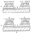
続いて、図4(A)に示したように、例えばMOCVD法により、n型GaAsよりなるバッファ層51,n型AlGaAs混晶よりなるn型クラッド層52,Alx Ga1-x As(但し、x≧0)混晶よりなる活性層53,p型AlGaAs混晶よりなるp型クラッド層54およびp型GaAsよりなるp型コンタクト層55を順次成長させる。
Subsequently, as shown in FIG. 4A, the
そののち、図4(B)に示したように、p型コンタクト層55の上にAlGaInP系レーザ素子24の形成予定領域に対応してレジスト膜R2 を形成する。続いて、このレジスト膜R2 をマスクとして、例えば、硫酸系のエッチング液を用いてp型コンタクト層55を選択的に除去し、フッ酸系のエッチング液を用いてp型クラッド層54,活性層53およびn型クラッド層52をそれぞれ選択的に除去し、塩酸系のエッチング液を用いてバッファ層51を選択的に除去する。そののち、レジスト膜R2 を除去する。
After that, as shown in FIG. 4B, a resist film R 2 is formed on the p-
レジスト膜R2 を除去したのち、図5(A)に示したように、例えば図示しない細い帯状のマスクを用いて、p型コンタクト層55およびp型クラッド層54の上層部にイオン注入法によりケイ素などのn型不純物を導入する。これにより、不純物が導入された領域は絶縁化され、電流ブロック領域56となる。
After removing the resist film R 2 , as shown in FIG. 5A, for example, by using a thin band-shaped mask (not shown), an ion implantation method is performed on the p-
電流ブロック領域56を形成したのち、図5(B)に示したように、p型コンタクト層44,55の表面およびその近傍に、例えば、ニッケル,白金および金を順次蒸着し、p側電極46,57をそれぞれ形成する。更に、基板22の裏面側を例えばラッピングおよびポリッシングすることにより、基板22の厚さを例えば100μm程度とする。
After forming the
続いて、この基板22の裏面側に、例えば、金とゲルマニウムとの合金,ニッケルおよび金を順次蒸着し、2つのレーザ素子24,26に共通のn側電極60を形成する。そののち、加熱処理を行い、p側電極46,57およびn側電極60をそれぞれ合金化する。更に、基板22を例えばp側電極46,57の長さ方向に対して垂直に所定の幅で劈開し、その劈開面に一対の反射鏡膜を形成する。これにより本実施の形態の2波長半導体レーザ20が作製される。
Subsequently, for example, an alloy of gold and germanium, nickel and gold are sequentially deposited on the back surface side of the
なお、この2波長半導体レーザ20は、例えば光ディスク装置(光ピックアップ)に用いられる。
The two-
図6は、その光ディスク装置の構成を模式的に表すものである。この光ディスク装置は、波長の異なる光を用いて光ディスクに記録されている情報をそれぞれ読み出し(再生)し、また光ディスクに情報を書き込む(記録)ためのものである。 FIG. 6 schematically shows the configuration of the optical disc apparatus. This optical disc apparatus is for reading (reproducing) information recorded on an optical disc using light having different wavelengths and writing (recording) information on the optical disc.
この光ディスク装置は、制御部111の制御に基づいて、2波長半導体レーザ20内のレーザ素子24,26のいずれか一方の出射光Lout を光ディスクDへ導くと共に、光ディスクDからの信号光(反射光Lref )読み取るための光学系、すなわち、ビームスプリッタ112,コリメータレンズ113,ミラー114,開口制限アパーチャ115,対物レンズ116,信号光検出用レンズ117,信号光検出用受光素子118および信号光再生回路119を備えている。信号光検出用受光素子118には、一方のAlGaInP系レーザ素子24から出射された650nm帯の赤色レーザ光を受光するための第1フォトダイオード118Aと、一方のAlGaAs系レーザ素子26から出射された780nm帯の赤色レーザ光を受光するための第2フォトダイオード118Bとが含まれている。
This optical disc apparatus guides the outgoing light L out of either one of the
この光ディスク装置では、2波長半導体レーザ20のAlGaInP系レーザ素子24またはAlGaAs系レーザ素子26から例えば強度の大きい出射光Lout が出射されると、この出射光Lout はビームスプリッタ112で反射し、コリメータレンズ113で平行光にされ、ミラー114で反射される。ミラー114で反射した出射光Lout は、開口制限アパーチャ115を通過したのち、対物レンズ116により集光されて光ディスクDに入射する。これにより、光ディスクDに情報が書き込まれる。また、2波長半導体レーザ20から微弱な出射光Lout が出射されると、この出射光Lout は、上述したように各光学系を経て光ディスクDに入射したのち、光ディスクDで反射する。この反射光Lref は、対物レンズ116,開口制限アパーチャ115,ミラー114,コリメータレンズ113およびビームスプリッタ112を経て、信号光検出用レンズ117を通過し、信号光検出用受光素子118に入射し、ここで電気信号に変換された後、信号光再生回路119において光ディスクDに書き込まれた情報の再生が行われる。
In this optical disc apparatus, when the emitted light L out having a large intensity is emitted from the
ここで、出射光Lout が、AlGaInP系レーザ素子24からの650nm帯の赤色レーザ光である場合には、信号光検出用受光素子118において第1フォトダイオード118A、また、AlGaAs系レーザ素子26から出射された780nm帯の赤色レーザ光である場合には、第2フォトダイオード118Bにそれぞれ受光される点を除いて、2つのレーザ素子24,26のレーザ光の経路は同じである。
Here, when the emitted light L out is 650 nm band red laser light from the AlGaInP-based
前述のようにAlGaInP系レーザ素子24およびAlGaAs系レーザ素子26の光軸同士が接近することから、読み出しまたは書き込みを行う際に、光ディスクDをDVDからCD、あるいはCDからDVDに切り換えるときのレンズシフト量が従来のモノシリック2波長半導体レーザに比べて著しく小さくなっているので、光学ピックアップの光学系の調整が容易になり、光学ピックアップの歩留りが向上する。また、レンズシフト量を小さくできることからレンズシフトに伴う光学収差を低減でき、DVD,CD等のディスクDからの信号のSN比(ジッター)を高く確保でき、安定した性能で光学ピックアップによる読み取りおよび書き込みを行うことができる。
As described above, since the optical axes of the
なお、記録媒体としては、CD,DVDに限らず、その他、CD−ROM(Read Onry Memory),CD−R,CD−RW,MD,DVD−ROMなどの既存の各種光ディスクは勿論のこと、DVD−RAM(Random Access Memory),DVD+RWあるいはDVD−R/RWなどのほか、更に高い面記録密度(例えば20Gバイト以上)を有する記録可能な光ディスク(例えば、次世代の光ディスク装置として提唱されているDVR(Digital Video Recorder)またはVDR(Video Disk Recorder )が挙げられるが、これらについても、本実施の形態の2波長半導体レーザ20を用いて記録・再生を行うことが可能となる。このような次世代の記録可能な大容量ディスクを利用することができれば、映像データを録画することができると共に、録画したデータ(画像)を良好な画質で操作性よく再生することができる。
Note that the recording medium is not limited to CD and DVD, but other various optical disks such as CD-ROM (Read Onry Memory), CD-R, CD-RW, MD, and DVD-ROM as well as DVD. -RAM (Random Access Memory), DVD + RW, DVD-R / RW, etc., as well as recordable optical discs having higher surface recording density (for example, 20 Gbytes or more) (for example, DVR proposed as the next generation optical disc apparatus) (Digital Video Recorder) or VDR (Video Disk Recorder) can be used, and these can also be recorded / reproduced by using the two-
なお、ここでは、2波長半導体レーザ20を光ディスク記録再生装置に適用した例について説明したが、光ディスク再生装置,光ディスク記録装置,光磁気ディスク(MO;Magneto-optical disk)などの記録・再生を行うための光磁気ディスク装置あるいは光通信装置などの光装置全般に適用できることは勿論、高温で動作する必要のある車載用の半導体レーザ装置を備えた機器などにも適用可能である。
Here, an example in which the two-
上記実施の形態では、AlGaAs系およびAlGaInP系の化合物よりなる各層をMOCVD法により形成する場合について説明したが、MBE(Molecular Beam Epitaxy)法やハイドライド気相成長法などの他の気相成長法により形成するようにしてもよい。 In the above embodiment, the case where each layer made of an AlGaAs-based compound and an AlGaInP-based compound is formed by the MOCVD method has been described. However, by other vapor phase growth methods such as MBE (Molecular Beam Epitaxy) method and hydride vapor phase growth method. You may make it form.
また、第1の発光素子としてのAlGaInP系レーザ素子24および第2の発光素子としてのAlGaAs系レーザ素子26の組成は、GaAs基板に格子整合する限り特に制約されるものではない。
Further, the composition of the AlGaInP-based
更に、素子としてはAlGaInP系/AlGaAs系の組み合わせに限られるものではなく、要は、主出射方向から見て、オフ基板の側面が結晶軸方向に対して時計廻り方向に所定の範囲(2〜15度)の角度で傾斜し、主出射面側から見て、一方(右側)の発光素子が、対向する2つの側面のうち左側が右側よりもなだらかな台形状の断面を有するものであればよい。 Further, the element is not limited to the combination of AlGaInP system / AlGaAs system. In short, when viewed from the main emission direction, the side surface of the off-substrate has a predetermined range (2 to 2) in the clockwise direction with respect to the crystal axis direction. If the light emitting element on one side (right side) has a gentler trapezoidal cross section than the right side, the left side of the two opposing side surfaces is inclined at an angle of 15 degrees) Good.
Claims (6)
主出射面(01−1)側から見たその両側面が、結晶軸(100)方向に対して(0−1−1)面から(011)面に向かう方向に所定の角度(オフ角)で傾斜してなる共通基板に、第1のn型クラッド層,第1の活性層,第1のp型クラッド層および第1のp型コンタクト層を順次成長させる工程と、
前記第1のp型コンタクト層および前記第1のp型クラッド層の上層部を選択的にエッチングして細い帯状のリッジ部を形成すると共に、前記リッジ部を、主出射面側から見て、対向する2つの側面のうち左側が右側よりもなだらかな台形状の断面を有する非対称なリッジ部とする工程と、
前記第1のp型コンタクト層および前記第1のp型クラッド層の側面を覆う絶縁層を形成する工程と、
前記第1のp型コンタクト層,前記第1のp型クラッド層,前記第1の活性層および前記第1のn型クラッド層を選択的に除去することにより、前記共通基板の(011)面側に、主出射面側から見て、対向する2つの側面のうち左側が右側よりもなだらかな台形状の断面を有する第1の発光素子を形成する工程と、
前記共通基板に、第2のn型クラッド層,第2の活性層,第2のp型クラッド層および第2のp型コンタクト層を順次成長させる工程と、
前記第2のp型コンタクト層,前記第2のp型クラッド層,前記第2の活性層および前記第2のn型クラッド層を選択的に除去する工程と、
前記第2のp型コンタクト層および前記第2のp型クラッド層の上層部に電流ブロック領域を形成することにより、前記共通基板の(0−1−1)面側に、前記第1の発光素子と対をなす第2の発光素子を形成する工程と
を含む半導体発光装置の製造方法。 A method for manufacturing a semiconductor light-emitting device having at least one set of light-emitting elements whose main emission surfaces are in the same direction at positions adjacent to the main surface of a common substrate,
The both side surfaces seen from the main emission surface (01-1) side have a predetermined angle (off angle) in the direction from the (0-1-1) plane to the (011) plane with respect to the crystal axis (100) direction. Sequentially growing a first n-type cladding layer, a first active layer, a first p-type cladding layer, and a first p-type contact layer on a common substrate inclined at
The upper layer portion of the first p-type contact layer and the first p-type cladding layer is selectively etched to form a thin band-shaped ridge portion, and the ridge portion is viewed from the main emission surface side, A step of forming an asymmetric ridge portion having a gentler trapezoidal cross section on the left side of the two opposing side surfaces than the right side;
Forming an insulating layer covering side surfaces of the first p-type contact layer and the first p-type cladding layer;
By selectively removing the first p-type contact layer, the first p-type cladding layer, the first active layer, and the first n-type cladding layer, the (011) plane of the common substrate Forming a first light emitting element having a trapezoidal cross-section with a gentler left side than the right side, as viewed from the main emission surface side, on the side;
Sequentially growing a second n-type cladding layer, a second active layer, a second p-type cladding layer, and a second p-type contact layer on the common substrate;
Selectively removing the second p-type contact layer, the second p-type cladding layer, the second active layer, and the second n-type cladding layer;
By forming a current block region in an upper layer portion of the second p-type contact layer and the second p-type cladding layer, the first light emission is formed on the (0-1-1) plane side of the common substrate. Forming a second light emitting element that forms a pair with the element.
請求項1記載の半導体発光装置の製造方法。 The method for manufacturing a semiconductor light emitting device according to claim 1, wherein the ridge portion of the first light emitting element is formed by wet etching using an etchant having an etching rate that is selective depending on a crystal orientation.
請求項2記載の半導体発光装置の製造方法。 The method for manufacturing a semiconductor light emitting device according to claim 2, wherein the current block region of the second light emitting element is formed by an ion implantation method.
請求項1記載の半導体発光装置の製造方法。 The method for manufacturing a semiconductor light emitting device according to claim 1, wherein an off angle of the substrate is not less than 2 degrees and not more than 15 degrees.
請求項1記載の半導体発光装置の製造方法。 The method of manufacturing a semiconductor light emitting device according to claim 1, wherein the substrate is a GaAs substrate, the first light emitting element is an AlGaInP laser element, and the second light emitting element is an AlGaAs laser element.
請求項5記載の半導体発光装置の製造方法。 The method for manufacturing a semiconductor light emitting device according to claim 5, wherein the first light emitting element emits laser light having a wavelength of 650 nm band and the second light emitting element emits laser light having a wavelength of 750 nm band.
Priority Applications (1)
| Application Number | Priority Date | Filing Date | Title |
|---|---|---|---|
| JP2009245841A JP5240156B2 (en) | 2002-02-21 | 2009-10-26 | Manufacturing method of semiconductor light emitting device |
Applications Claiming Priority (3)
| Application Number | Priority Date | Filing Date | Title |
|---|---|---|---|
| JP2002044651 | 2002-02-21 | ||
| JP2002044651 | 2002-02-21 | ||
| JP2009245841A JP5240156B2 (en) | 2002-02-21 | 2009-10-26 | Manufacturing method of semiconductor light emitting device |
Related Parent Applications (1)
| Application Number | Title | Priority Date | Filing Date |
|---|---|---|---|
| JP2003570434A Division JPWO2003071642A1 (en) | 2002-02-21 | 2003-02-20 | Semiconductor light emitting device and optical disk device using the same |
Publications (2)
| Publication Number | Publication Date |
|---|---|
| JP2010021585A true JP2010021585A (en) | 2010-01-28 |
| JP5240156B2 JP5240156B2 (en) | 2013-07-17 |
Family
ID=27750560
Family Applications (2)
| Application Number | Title | Priority Date | Filing Date |
|---|---|---|---|
| JP2003570434A Pending JPWO2003071642A1 (en) | 2002-02-21 | 2003-02-20 | Semiconductor light emitting device and optical disk device using the same |
| JP2009245841A Expired - Fee Related JP5240156B2 (en) | 2002-02-21 | 2009-10-26 | Manufacturing method of semiconductor light emitting device |
Family Applications Before (1)
| Application Number | Title | Priority Date | Filing Date |
|---|---|---|---|
| JP2003570434A Pending JPWO2003071642A1 (en) | 2002-02-21 | 2003-02-20 | Semiconductor light emitting device and optical disk device using the same |
Country Status (6)
| Country | Link |
|---|---|
| US (2) | US6995399B2 (en) |
| JP (2) | JPWO2003071642A1 (en) |
| KR (1) | KR100918328B1 (en) |
| CN (1) | CN1264259C (en) |
| TW (1) | TWI228338B (en) |
| WO (1) | WO2003071642A1 (en) |
Cited By (2)
| Publication number | Priority date | Publication date | Assignee | Title |
|---|---|---|---|---|
| JPWO2019021802A1 (en) * | 2017-07-26 | 2020-05-28 | パナソニック株式会社 | Semiconductor laser device and semiconductor laser device |
| JPWO2019216364A1 (en) * | 2018-05-09 | 2021-05-20 | 国立研究開発法人理化学研究所 | Optical equipment and photoacoustic microscope |
Families Citing this family (12)
| Publication number | Priority date | Publication date | Assignee | Title |
|---|---|---|---|---|
| CN1264259C (en) * | 2002-02-21 | 2006-07-12 | 索尼公司 | Semiconductor light emitting device and optical disk unit using it |
| JP2006120668A (en) * | 2004-10-19 | 2006-05-11 | Mitsubishi Electric Corp | Semiconductor laser |
| JP2006313875A (en) * | 2005-04-08 | 2006-11-16 | Mitsubishi Electric Corp | Semiconductor laser device |
| KR100848759B1 (en) * | 2007-08-07 | 2008-07-25 | 김정수 | Semiconductor laser diode chip having a plurality of waveguide |
| JP5347541B2 (en) * | 2009-01-30 | 2013-11-20 | 三洋電機株式会社 | Semiconductor laser device and semiconductor laser device including the same |
| JP2011049295A (en) * | 2009-08-26 | 2011-03-10 | Toshiba Corp | Semiconductor laser device |
| JP5493624B2 (en) * | 2009-09-15 | 2014-05-14 | ソニー株式会社 | Image display device and electronic device |
| KR20140006485A (en) * | 2012-07-05 | 2014-01-16 | 삼성전자주식회사 | Semiconductor light emitting device having a multi-cell array and method for manufacturing the same |
| KR20150101783A (en) * | 2014-02-27 | 2015-09-04 | 서울바이오시스 주식회사 | Light emitting diode and method of fabricating the same |
| JP6289640B2 (en) * | 2014-07-25 | 2018-03-07 | 三菱電機株式会社 | Semiconductor laser device |
| US11398715B2 (en) * | 2018-02-26 | 2022-07-26 | Panasonic Holdings Corporation | Semiconductor light emitting device |
| KR102601950B1 (en) * | 2018-11-16 | 2023-11-14 | 삼성전자주식회사 | Light emitting diode, manufacturing method of light emitting diode and display device including light emitting diode |
Citations (2)
| Publication number | Priority date | Publication date | Assignee | Title |
|---|---|---|---|---|
| JP2000349387A (en) * | 1999-06-02 | 2000-12-15 | Sony Corp | Semiconductor laser and its manufacture |
| JP2001144373A (en) * | 1999-11-16 | 2001-05-25 | Matsushita Electronics Industry Corp | Method of manufacturing semiconductor laser |
Family Cites Families (8)
| Publication number | Priority date | Publication date | Assignee | Title |
|---|---|---|---|---|
| JP3281805B2 (en) * | 1996-06-28 | 2002-05-13 | 三洋電機株式会社 | Semiconductor laser device |
| JPH11186651A (en) * | 1997-12-19 | 1999-07-09 | Sony Corp | Integrated semiconductor light-emitting device |
| JP4147602B2 (en) * | 1998-02-02 | 2008-09-10 | ソニー株式会社 | Self-oscillation type semiconductor laser |
| JP2000244060A (en) * | 1998-12-22 | 2000-09-08 | Sony Corp | Semiconductor light emitting device and its manufacture |
| JP2000195827A (en) * | 1998-12-25 | 2000-07-14 | Oki Electric Ind Co Ltd | Led array chip and its manufacture, and dicing device |
| US6813290B1 (en) * | 1999-11-25 | 2004-11-02 | Matsushita Electric Industrial Co., Ltd. | Semiconductor laser device and method for fabricating the same |
| JP2001244574A (en) * | 1999-12-22 | 2001-09-07 | Asahi Glass Co Ltd | Two-wavelength light source device and optical head device |
| CN1264259C (en) * | 2002-02-21 | 2006-07-12 | 索尼公司 | Semiconductor light emitting device and optical disk unit using it |
-
2003
- 2003-02-20 CN CNB038001373A patent/CN1264259C/en not_active Expired - Fee Related
- 2003-02-20 WO PCT/JP2003/001833 patent/WO2003071642A1/en active Application Filing
- 2003-02-20 KR KR1020037013697A patent/KR100918328B1/en not_active IP Right Cessation
- 2003-02-20 US US10/473,688 patent/US6995399B2/en not_active Expired - Fee Related
- 2003-02-20 JP JP2003570434A patent/JPWO2003071642A1/en active Pending
- 2003-02-21 TW TW092103651A patent/TWI228338B/en not_active IP Right Cessation
-
2005
- 2005-06-23 US US11/165,014 patent/US7141827B2/en not_active Expired - Fee Related
-
2009
- 2009-10-26 JP JP2009245841A patent/JP5240156B2/en not_active Expired - Fee Related
Patent Citations (2)
| Publication number | Priority date | Publication date | Assignee | Title |
|---|---|---|---|---|
| JP2000349387A (en) * | 1999-06-02 | 2000-12-15 | Sony Corp | Semiconductor laser and its manufacture |
| JP2001144373A (en) * | 1999-11-16 | 2001-05-25 | Matsushita Electronics Industry Corp | Method of manufacturing semiconductor laser |
Cited By (4)
| Publication number | Priority date | Publication date | Assignee | Title |
|---|---|---|---|---|
| JPWO2019021802A1 (en) * | 2017-07-26 | 2020-05-28 | パナソニック株式会社 | Semiconductor laser device and semiconductor laser device |
| JPWO2019216364A1 (en) * | 2018-05-09 | 2021-05-20 | 国立研究開発法人理化学研究所 | Optical equipment and photoacoustic microscope |
| JP7291959B2 (en) | 2018-05-09 | 2023-06-16 | 国立研究開発法人理化学研究所 | Optical device and photoacoustic microscope |
| US11959882B2 (en) | 2018-05-09 | 2024-04-16 | Riken | Optical device and photoacoustic microscope |
Also Published As
| Publication number | Publication date |
|---|---|
| US20050258434A1 (en) | 2005-11-24 |
| CN1498447A (en) | 2004-05-19 |
| US6995399B2 (en) | 2006-02-07 |
| TW200405631A (en) | 2004-04-01 |
| US20040113157A1 (en) | 2004-06-17 |
| CN1264259C (en) | 2006-07-12 |
| WO2003071642A1 (en) | 2003-08-28 |
| JP5240156B2 (en) | 2013-07-17 |
| US7141827B2 (en) | 2006-11-28 |
| JPWO2003071642A1 (en) | 2005-06-16 |
| TWI228338B (en) | 2005-02-21 |
| KR100918328B1 (en) | 2009-09-22 |
| KR20040078172A (en) | 2004-09-09 |
Similar Documents
| Publication | Publication Date | Title |
|---|---|---|
| JP5240156B2 (en) | Manufacturing method of semiconductor light emitting device | |
| JP3486900B2 (en) | Light emitting device and optical device using the same | |
| JPH1146039A (en) | Dual wavelength monolithically integrated vertical cavity surface-exiting lasers(vcsel) and method of fabrication | |
| JP2004193330A (en) | Monolithic multiwavelength laser element and its manufacturing method | |
| JP2000244060A (en) | Semiconductor light emitting device and its manufacture | |
| KR100782285B1 (en) | Semiconductor laser apparatus, laser coupler, data reproduction apparatus, data recording apparatus and production method of semiconductor laser apparatus | |
| US6930024B2 (en) | Semiconductor laser device and method for fabricating the same | |
| US6781944B1 (en) | Optical information processor with monolithically integrated light emitting device, light receiving devices and optics | |
| JP2002217499A (en) | Semiconductor laser element and its manufacturing method, and optical pickup using the same | |
| JP2003298193A (en) | Light emitting device, optical device employing it and method for fabricating light emitting device | |
| JP2006080307A (en) | Semiconductor laser array, its manufacturing method and multiwavelength semiconductor laser device | |
| JP3818815B2 (en) | Semiconductor laser device and manufacturing method thereof | |
| JP3493276B2 (en) | Semiconductor laser device and method of manufacturing the same | |
| KR100360143B1 (en) | Semiconductor laser device and process for manufacturing the same | |
| JP2000196203A (en) | Semiconductor laser and its manufacture | |
| JP2000036639A (en) | Semiconductor laser device, its manufacture, and pickup device | |
| JP2001250255A (en) | Optical apparatus and optical disk device | |
| JP4821829B2 (en) | Manufacturing method of semiconductor light emitting device | |
| JP4595929B2 (en) | Method for manufacturing light emitting device | |
| JP2001244573A (en) | Method of manufacturing semiconductor light emitting device | |
| JP2004047096A (en) | Optical head for optical recording and reproducing device | |
| JP2000187876A (en) | Optical device and optical disk drive | |
| WO2005015701A1 (en) | Light source using multiple beam laser | |
| JP2004079168A (en) | Optical head for optical recording and reproducing device | |
| JP2005166817A (en) | Semiconductor laser device and manufacturing method thereof |
Legal Events
| Date | Code | Title | Description |
|---|---|---|---|
| A521 | Request for written amendment filed |
Free format text: JAPANESE INTERMEDIATE CODE: A523 Effective date: 20091027 |
|
| A621 | Written request for application examination |
Free format text: JAPANESE INTERMEDIATE CODE: A621 Effective date: 20091027 |
|
| A131 | Notification of reasons for refusal |
Free format text: JAPANESE INTERMEDIATE CODE: A131 Effective date: 20120905 |
|
| A521 | Request for written amendment filed |
Free format text: JAPANESE INTERMEDIATE CODE: A523 Effective date: 20121029 |
|
| TRDD | Decision of grant or rejection written | ||
| A01 | Written decision to grant a patent or to grant a registration (utility model) |
Free format text: JAPANESE INTERMEDIATE CODE: A01 Effective date: 20130305 |
|
| A61 | First payment of annual fees (during grant procedure) |
Free format text: JAPANESE INTERMEDIATE CODE: A61 Effective date: 20130318 |
|
| FPAY | Renewal fee payment (event date is renewal date of database) |
Free format text: PAYMENT UNTIL: 20160412 Year of fee payment: 3 |
|
| FPAY | Renewal fee payment (event date is renewal date of database) |
Free format text: PAYMENT UNTIL: 20160412 Year of fee payment: 3 |
|
| LAPS | Cancellation because of no payment of annual fees |