JP2010020863A - 三次元メモリデバイス - Google Patents
三次元メモリデバイス Download PDFInfo
- Publication number
- JP2010020863A JP2010020863A JP2008182410A JP2008182410A JP2010020863A JP 2010020863 A JP2010020863 A JP 2010020863A JP 2008182410 A JP2008182410 A JP 2008182410A JP 2008182410 A JP2008182410 A JP 2008182410A JP 2010020863 A JP2010020863 A JP 2010020863A
- Authority
- JP
- Japan
- Prior art keywords
- word line
- groups
- mat
- cell
- bit
- Prior art date
- Legal status (The legal status is an assumption and is not a legal conclusion. Google has not performed a legal analysis and makes no representation as to the accuracy of the status listed.)
- Granted
Links
Images


Classifications
-
- G—PHYSICS
- G11—INFORMATION STORAGE
- G11C—STATIC STORES
- G11C5/00—Details of stores covered by group G11C11/00
- G11C5/02—Disposition of storage elements, e.g. in the form of a matrix array
-
- G—PHYSICS
- G11—INFORMATION STORAGE
- G11C—STATIC STORES
- G11C29/00—Checking stores for correct operation ; Subsequent repair; Testing stores during standby or offline operation
- G11C29/04—Detection or location of defective memory elements, e.g. cell constructio details, timing of test signals
- G11C29/50—Marginal testing, e.g. race, voltage or current testing
-
- G—PHYSICS
- G11—INFORMATION STORAGE
- G11C—STATIC STORES
- G11C29/00—Checking stores for correct operation ; Subsequent repair; Testing stores during standby or offline operation
- G11C29/70—Masking faults in memories by using spares or by reconfiguring
- G11C29/78—Masking faults in memories by using spares or by reconfiguring using programmable devices
- G11C29/83—Masking faults in memories by using spares or by reconfiguring using programmable devices with reduced power consumption
- G11C29/832—Masking faults in memories by using spares or by reconfiguring using programmable devices with reduced power consumption with disconnection of faulty elements
-
- G—PHYSICS
- G11—INFORMATION STORAGE
- G11C—STATIC STORES
- G11C5/00—Details of stores covered by group G11C11/00
- G11C5/02—Disposition of storage elements, e.g. in the form of a matrix array
- G11C5/025—Geometric lay-out considerations of storage- and peripheral-blocks in a semiconductor storage device
-
- G—PHYSICS
- G11—INFORMATION STORAGE
- G11C—STATIC STORES
- G11C5/00—Details of stores covered by group G11C11/00
- G11C5/06—Arrangements for interconnecting storage elements electrically, e.g. by wiring
- G11C5/066—Means for reducing external access-lines for a semiconductor memory clip, e.g. by multiplexing at least address and data signals
-
- G—PHYSICS
- G11—INFORMATION STORAGE
- G11C—STATIC STORES
- G11C8/00—Arrangements for selecting an address in a digital store
- G11C8/12—Group selection circuits, e.g. for memory block selection, chip selection, array selection
-
- G—PHYSICS
- G11—INFORMATION STORAGE
- G11C—STATIC STORES
- G11C8/00—Arrangements for selecting an address in a digital store
- G11C8/14—Word line organisation; Word line lay-out
-
- G—PHYSICS
- G11—INFORMATION STORAGE
- G11C—STATIC STORES
- G11C29/00—Checking stores for correct operation ; Subsequent repair; Testing stores during standby or offline operation
- G11C29/04—Detection or location of defective memory elements, e.g. cell constructio details, timing of test signals
- G11C2029/0409—Online test
-
- G—PHYSICS
- G11—INFORMATION STORAGE
- G11C—STATIC STORES
- G11C29/00—Checking stores for correct operation ; Subsequent repair; Testing stores during standby or offline operation
- G11C29/04—Detection or location of defective memory elements, e.g. cell constructio details, timing of test signals
- G11C29/50—Marginal testing, e.g. race, voltage or current testing
- G11C2029/5006—Current
Landscapes
- Engineering & Computer Science (AREA)
- Microelectronics & Electronic Packaging (AREA)
- Semiconductor Memories (AREA)
Abstract
【解決手段】メモリセルが二次元マトリクス状に配列されたマットを複数層積層して構成され、各マット内でメモリセル選択を行うアクセス信号線とデータ線とがそれぞれ隣接マット間で共有された三次元メモリデバイスであって、積層されたマットが3つ以上の複数グループに分けられ、その複数グループの一つが選択されるときに、残りのグループの一部においてメモリセルがリーク電流の流れる状態にバイアスされ、残部においてメモリセルがリーク電流の流れない状態にバイアスされる。
【選択図】図17
Description
Y. Hosoi et al, "High Speed Unipolar Switching Resistance RAM(RRAM) Technology" IEEE International Electron Devices Meeting 2006 Technical Digest p.793-796
積層されたマットが3つ以上の複数グループに分けられ、その複数グループの一つが選択されるときに、残りのグループの一部においてメモリセルがリーク電流の流れる状態にバイアスされ、残部においてメモリセルがリーク電流の流れない状態にバイアスされることを特徴とする。
半導体基板と、
前記半導体基板上にメモリセルが二次元マトリクス状に配列されたマットを複数層積層して構成され、各マット内でメモリセル選択を行うアクセス信号線とデータ線とがそれぞれ隣接マット間で共有された三次元セルアレイと、
前記半導体基板の前記三次元セルアレイ下に形成されて、前記三次元セルアレイの読み出し及び書き込み制御を行う制御回路とを備え、
前記制御回路は、前記三次元セルアレイのマットを3つ以上の複数グループに分けて、その複数グループの一つを選択するときに、残りのグループの一部を同時に選択し、残部を非選択とするグループ選択回路を有する
ことを特徴とする。
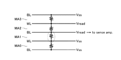
図1は、実施の形態による三次元(3D)セルアレイ構造のReRAMについて、その3Dセルアレイブロック1と下地制御回路2の構成概要を示している。ここでは、セルアレイブロック1は、説明を簡単にするため、4層のセルアレイMA0〜MA3が積層された例を示している。
実施の形態の技術的要素をまとめると、次の通りである。
具体的な実施の形態の説明に先立って、先ず図4を参照して、ビット線BLとワード線WLをそれぞれ隣接セルアレイ間で共有する方式とした3D−ReRAMにおけるリーク電流の影響、具体的に選択セルについて、どれだけ離れたマットの不良セルの影響が現れるかを検討する。
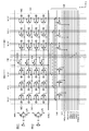
図6は、16層マット構成で、上に説明した2グループ分けの場合(binaryの場合)である。左側に異なるワード線とビット線に属するセルをイメージして16層のマットを二つのメモリセルの柱として示す。下線を付した番号が、下から数えたマット番号である。グループ番号は、バイナリの場合は0と1がワード線ごとに交互に繰り返される。
図7は、同様の16マット構成で3グループ分けの場合(ternary の場合)である。即ちワード線群WL0,WL3,WL6をグループ0、ワード線群WL1,WL4,WL7をグループ1、ワード線群WL2,WL5,WL8をグループ2と設定している。
図8は、同様の16マット構成で4グループ分けの場合(quadrupleの場合)である。即ちワード線群WL0,WL4,WL8をグループ0、ワード線群WL1,WL5をグループ1、ワード線群WL2,WL6をグループ2、ワード線群WL3,WL7をグループ3、と設定している。
上述のように、ワード線の選択グループを、binary, ternary, quadruple と増やすと、リーク電流の選択ワード線グループへの影響を小さく出来ることが分かった。この場合、ワード線はマット間で共用されるため、グループ間の選択ロジックに工夫がいる。次にこのワード線選択ロジックを説明する。
以上、ワード線グループの分割とマット選択の規則についてまとめたが、これらを実際に3Dセルアレイに適用する際の具体的な方法について説明する。まずワード線を3以上のグループに分けた場合について、セルアレイのリークの影響を具体的に見てみる。
図12は、ワード線及びビット線選択回路部の詳細構成を示している。3Dセルアレイは、センスアンプ(SA)106を共有するビット線群の範囲をひとつのセルアレイユニット(以下、スタンバイユニットという)100として、それらのビット線群の一つがビット線選択回路103により選択されて、ローカルバスLB_mに接続される。ビット線選択回路103としてここでは簡略に選択トランジスタであるNMOSトランジスタQN2のみ示している。
図13は、メモリチップの構成と活性化の選択のひとつの方式を説明するための図である。ここでは、一つのセルアレイブロックが32マットで、1マットが1k本のワード線を有し、一つのメインワード線を選択することにより複数の部分ワード線ドライバに選択信号が送られて、複数のワード線が選択される、ダブルワード線スキーム方式の場合を想定している。
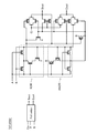
ternaryの場合(i=3)について具体的なワード線選択信号発生回路を検討する。
・(m−1)br:5ビット加算回路(5 bit adder)201にmのアドレスビットと、1の5ビットの補数11111を入力して加算結果のm−1を求める。この結果をmod 6の剰余を求める剰余回路(5 bit residue(6))202に入力して、剰余の2進数表現(m−1)br(r=0〜4)を得る。
・(m)br:5ビットのmのアドレスビットをmod 6の剰余を求める剰余回路(5 bit residue(6))203に入力して剰余の2進数表現(m)br(r=0〜4) を得る。
・(m+1)br:5ビット加算回路(5 bit adder)204にmのアドレスビットと、1の5ビット表現00001を入力して加算結果のm+1を求める。この結果を、mod 6の剰余を求める剰余回路(5 bit residue(6))205に入力して剰余の2進数表現(m+1)br(r=0〜4)を得る。
・(m+2)br:5ビット加算回路(5 bit adder)206にmのアドレスビットと、2の5ビット表現00010を入力して加算結果のm+2を求める。この結果をmod 6の剰余を求める剰余回路(5 bit residue(6))207に入力して剰余の2進数表現(m+2)br(r=0〜4)を得る。
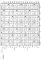
次に、quadrupleの場合(i=4)の具体的なワード線グループ選択信号発生回路を検討する。マットの総数を32としマット番号がA10〜A14の5ビットで2進表示されるものとする。各アドレスビットとmの関係は、図26の上側の表に示した通りである。選択信号WGcの0,1,2,3とmとmod 8の関係は下の表に示した通りである。
・(m−1)bm:5ビット加算回路(5 bit adder)301にmのアドレスビットと、1の5ビットの補数11111を入力して加算結果のm−1を求める。この結果をmod 8の剰余を求める剰余回路(5 bit residue(8))302に入力して、剰余の2進数表現(m−1)bm(m=0〜4)を得る。
・(m)bm:5ビットのmのアドレスビットをmod 8の剰余を求める剰余回路(5 bit residue(8))303に入力して剰余の2進数表現(m)bm(m=0〜4) を得る。
・(m+1)bm:5ビット加算回路(5 bit adder)304にmのアドレスビットと、1の5ビット表現00001を入力して加算結果のm+1を求める。この結果を、mod 8の剰余を求める剰余回路(5 bit residue(8))305に入力して剰余の2進数表現(m+1)bm(m=0〜4)を得る。
・(m+2)bm:5ビット加算回路(5 bit adder)306にmのアドレスビットと、2の5ビット表現00010を入力して加算結果のm+2を求める。この結果をmod 8の剰余を求める剰余回路(5 bit residue(8))307に入力して剰余の2進数表現(m+2)bm(m=0〜4)を得る。
Claims (5)
- メモリセルが二次元マトリクス状に配列されたマットを複数層積層して構成され、各マット内でメモリセル選択を行うアクセス信号線とデータ線とがそれぞれ隣接マット間で共有された三次元メモリデバイスにおいて、
積層されたマットが3つ以上の複数グループに分けられ、その複数グループの一つが選択されるときに、残りのグループの一部においてメモリセルがリーク電流の流れる状態にバイアスされ、残部においてメモリセルがリーク電流の流れない状態にバイアスされる
ことを特徴とする三次元メモリデバイス。 - 前記各マットは、前記アクセス信号線とデータ線のクロスポイントに、電圧印加により抵抗値を可逆的に設定できる可変抵抗素子とダイオードの直列接続により構成されたメモリセルを配置して構成され、
前記残りグループの一部において、アクセス信号線とデータ線の間がダイオードが逆バイアスの状態に設定され、前記残部において、アクセス信号線とデータ線の間がダイオードが略ゼロバイアスの状態に設定される
ことを特徴とする請求項1記載の三次元メモリデバイス。 - 半導体基板と、
前記半導体基板上にメモリセルが二次元マトリクス状に配列されたマットを複数層積層して構成され、各マット内でメモリセル選択を行うアクセス信号線とデータ線とがそれぞれ隣接マット間で共有された三次元セルアレイと、
前記半導体基板の前記三次元セルアレイ下に形成されて、前記三次元セルアレイの読み出し及び書き込み制御を行う制御回路とを備え、
前記制御回路は、前記三次元セルアレイのマットを3つ以上の複数グループに分けて、その複数グループの一つを選択するときに、残りのグループの一部を同時に選択し、残部を非選択とするグループ選択回路を有する
ことを特徴とする三次元メモリデバイス。 - 前記グループ選択回路は、
入力されるアドレスビットに基づいて選択メモリセルを含む選択グループに属する複数のマット番号を、2i(iは、グループ数)を法とする既約剰余として計算する計算回路と、
前記計算回路の結果に基づいて、前記複数グループの一つを選択する第1の選択信号及び、前記残りのグループの一部を同時に選択する第2の選択信号をデコードするグループ選択信号デコード回路とを有する
ことを特徴とする請求項3記載の三次元メモリデバイス。 - 前記三次元セルアレイの各マットは、前記アクセス信号線とデータ線のクロスポイントに、電圧印加により抵抗値を可逆的に設定できる可変抵抗素子とダイオードの直列接続により構成されたメモリセルを配置して構成され、
前記三次元セルアレイ内で前記複数グループの一つが選択されるときに、残りのグループの一部においてアクセス信号線とデータ線の間がダイオードが逆バイアスの状態に設定され、残部においてメモリセルがリークのない非活性状態に設定される
ことを特徴とする請求項3記載の三次元メモリデバイス。
Priority Applications (2)
| Application Number | Priority Date | Filing Date | Title |
|---|---|---|---|
| JP2008182410A JP5085446B2 (ja) | 2008-07-14 | 2008-07-14 | 三次元メモリデバイス |
| US12/501,116 US7889538B2 (en) | 2008-07-14 | 2009-07-10 | Three-dimensional memory device |
Applications Claiming Priority (1)
| Application Number | Priority Date | Filing Date | Title |
|---|---|---|---|
| JP2008182410A JP5085446B2 (ja) | 2008-07-14 | 2008-07-14 | 三次元メモリデバイス |
Publications (2)
| Publication Number | Publication Date |
|---|---|
| JP2010020863A true JP2010020863A (ja) | 2010-01-28 |
| JP5085446B2 JP5085446B2 (ja) | 2012-11-28 |
Family
ID=41505009
Family Applications (1)
| Application Number | Title | Priority Date | Filing Date |
|---|---|---|---|
| JP2008182410A Expired - Fee Related JP5085446B2 (ja) | 2008-07-14 | 2008-07-14 | 三次元メモリデバイス |
Country Status (2)
| Country | Link |
|---|---|
| US (1) | US7889538B2 (ja) |
| JP (1) | JP5085446B2 (ja) |
Cited By (12)
| Publication number | Priority date | Publication date | Assignee | Title |
|---|---|---|---|---|
| JP2011165240A (ja) * | 2010-02-05 | 2011-08-25 | Toshiba Corp | 半導体記憶装置 |
| KR101080801B1 (ko) | 2011-07-29 | 2011-11-07 | 아카데미정보통신 (주) | 입체적 매트릭스 회로를 통한 음향 및 영상 제어 시스템 |
| JP2012256847A (ja) * | 2011-03-10 | 2012-12-27 | Semiconductor Energy Lab Co Ltd | メモリ装置、及びメモリ装置の作製方法 |
| JP2012256837A (ja) * | 2011-01-26 | 2012-12-27 | Semiconductor Energy Lab Co Ltd | 記憶装置、及び半導体装置 |
| JP5283805B1 (ja) * | 2011-11-22 | 2013-09-04 | パナソニック株式会社 | 抵抗変化型不揮発性記憶装置、および抵抗変化型不揮発性記憶装置のアクセス方法 |
| US8675388B2 (en) | 2010-09-21 | 2014-03-18 | Kabushiki Kaisha Toshiba | Nonvolatile semiconductor memory device |
| US8687406B2 (en) | 2012-03-26 | 2014-04-01 | Kabushiki Kaisha Toshiba | Semiconductor memory device and method of controlling the same |
| US9190146B2 (en) | 2013-02-28 | 2015-11-17 | Kabushiki Kaisha Toshiba | Variable resistance memory system with redundancy lines and shielded bit lines |
| US9214226B2 (en) | 2011-03-24 | 2015-12-15 | Kabushiki Kaisha Toshiba | Semiconductor memory device |
| JP2016213493A (ja) * | 2010-09-14 | 2016-12-15 | 株式会社半導体エネルギー研究所 | 半導体装置 |
| JP2020511778A (ja) * | 2017-02-16 | 2020-04-16 | マイクロン テクノロジー,インク. | 活性化境界キルトアーキテクチャのメモリ |
| US11170850B2 (en) | 2017-02-16 | 2021-11-09 | Micron Technology, Inc. | Efficient utilization of memory die area |
Families Citing this family (20)
| Publication number | Priority date | Publication date | Assignee | Title |
|---|---|---|---|---|
| JP2012069217A (ja) | 2010-09-24 | 2012-04-05 | Toshiba Corp | 不揮発性半導体記憶装置 |
| JP5542742B2 (ja) | 2011-05-26 | 2014-07-09 | 株式会社東芝 | 半導体記憶装置 |
| US8913443B2 (en) | 2011-09-19 | 2014-12-16 | Conversant Intellectual Property Management Inc. | Voltage regulation for 3D packages and method of manufacturing same |
| US9110778B2 (en) * | 2012-11-08 | 2015-08-18 | International Business Machines Corporation | Address generation in an active memory device |
| US9129674B2 (en) * | 2013-06-27 | 2015-09-08 | Intel Corporation | Hybrid memory device |
| KR102187485B1 (ko) | 2014-02-21 | 2020-12-08 | 삼성전자주식회사 | 불휘발성 메모리 장치 및 그것의 센싱 방법 |
| KR102161748B1 (ko) | 2014-08-05 | 2020-10-05 | 삼성전자 주식회사 | 저항성 메모리 장치 및 저항성 메모리 장치의 동작 방법 |
| US9947682B2 (en) * | 2014-11-18 | 2018-04-17 | Sandisk Technologies Llc | Three dimensional non-volatile memory with separate source lines |
| KR102259943B1 (ko) | 2014-12-08 | 2021-06-04 | 삼성전자주식회사 | 멀티 플래인을 포함하는 불 휘발성 메모리 장치 |
| KR20170106343A (ko) | 2015-01-23 | 2017-09-20 | 휴렛 팩커드 엔터프라이즈 디벨롭먼트 엘피 | 크로스바 어레이 내의 출력 신호 감지 |
| JP6901831B2 (ja) | 2015-05-26 | 2021-07-14 | 株式会社半導体エネルギー研究所 | メモリシステム、及び情報処理システム |
| JP6773453B2 (ja) | 2015-05-26 | 2020-10-21 | 株式会社半導体エネルギー研究所 | 記憶装置及び電子機器 |
| KR102398666B1 (ko) | 2015-08-19 | 2022-05-16 | 삼성전자주식회사 | 비휘발성 메모리 장치 및 이를 포함하는 비휘발성 메모리 시스템 |
| US9715924B2 (en) | 2015-10-22 | 2017-07-25 | Sandisk Technologies Llc | Three dimensional non-volatile memory with current sensing programming status |
| US20170117036A1 (en) | 2015-10-22 | 2017-04-27 | Sandisk Technologies Llc | Source line driver for three dimensional non-volatile memory |
| KR102403733B1 (ko) | 2017-12-01 | 2022-05-30 | 삼성전자주식회사 | 메모리 소자 |
| US11144228B2 (en) * | 2019-07-11 | 2021-10-12 | Micron Technology, Inc. | Circuit partitioning for a memory device |
| US10957681B1 (en) | 2019-08-28 | 2021-03-23 | Micron Technology, Inc. | Integrated assemblies comprising sense-amplifier-circuitry and wordline-driver-circuitry under memory cells of a memory array |
| US11487454B2 (en) * | 2019-12-05 | 2022-11-01 | Sandisk Technologies Llc | Systems and methods for defining memory sub-blocks |
| US12087350B2 (en) * | 2020-09-25 | 2024-09-10 | Intel Corporation | Multi-deck non-volatile memory architecture with improved wordline bus and bitline bus configuration |
Citations (5)
| Publication number | Priority date | Publication date | Assignee | Title |
|---|---|---|---|---|
| JP2001168294A (ja) * | 1999-12-09 | 2001-06-22 | Seiko Epson Corp | メモリデバイス及びその製造方法、並びに電子機器 |
| JP2005522045A (ja) * | 2002-04-04 | 2005-07-21 | 株式会社東芝 | 相変化メモリ装置 |
| JP2006514440A (ja) * | 2003-04-03 | 2006-04-27 | 株式会社東芝 | 相変化メモリ装置 |
| JP2007536680A (ja) * | 2004-05-03 | 2007-12-13 | ユニティ・セミコンダクター・コーポレーション | 不揮発性プログラマブルメモリ |
| JP2008123595A (ja) * | 2006-11-10 | 2008-05-29 | Matsushita Electric Ind Co Ltd | 半導体記憶装置 |
Family Cites Families (11)
| Publication number | Priority date | Publication date | Assignee | Title |
|---|---|---|---|---|
| US6856572B2 (en) * | 2000-04-28 | 2005-02-15 | Matrix Semiconductor, Inc. | Multi-headed decoder structure utilizing memory array line driver with dual purpose driver device |
| US6618295B2 (en) * | 2001-03-21 | 2003-09-09 | Matrix Semiconductor, Inc. | Method and apparatus for biasing selected and unselected array lines when writing a memory array |
| US6504753B1 (en) * | 2001-03-21 | 2003-01-07 | Matrix Semiconductor, Inc. | Method and apparatus for discharging memory array lines |
| US6545898B1 (en) * | 2001-03-21 | 2003-04-08 | Silicon Valley Bank | Method and apparatus for writing memory arrays using external source of high programming voltage |
| US7623370B2 (en) * | 2002-04-04 | 2009-11-24 | Kabushiki Kaisha Toshiba | Resistance change memory device |
| US7081377B2 (en) * | 2002-06-27 | 2006-07-25 | Sandisk 3D Llc | Three-dimensional memory |
| US6917539B2 (en) * | 2002-08-02 | 2005-07-12 | Unity Semiconductor Corporation | High-density NVRAM |
| US7061037B2 (en) * | 2004-07-06 | 2006-06-13 | Maglabs, Inc. | Magnetic random access memory with multiple memory layers and improved memory cell selectivity |
| US7570523B2 (en) * | 2006-07-31 | 2009-08-04 | Sandisk 3D Llc | Method for using two data busses for memory array block selection |
| KR100827697B1 (ko) * | 2006-11-10 | 2008-05-07 | 삼성전자주식회사 | 3차원 구조를 가지는 반도체 메모리 장치 및 셀 어레이구조 |
| CN101548336B (zh) * | 2007-06-22 | 2012-07-11 | 松下电器产业株式会社 | 电阻变化型非易失性存储装置 |
-
2008
- 2008-07-14 JP JP2008182410A patent/JP5085446B2/ja not_active Expired - Fee Related
-
2009
- 2009-07-10 US US12/501,116 patent/US7889538B2/en active Active
Patent Citations (5)
| Publication number | Priority date | Publication date | Assignee | Title |
|---|---|---|---|---|
| JP2001168294A (ja) * | 1999-12-09 | 2001-06-22 | Seiko Epson Corp | メモリデバイス及びその製造方法、並びに電子機器 |
| JP2005522045A (ja) * | 2002-04-04 | 2005-07-21 | 株式会社東芝 | 相変化メモリ装置 |
| JP2006514440A (ja) * | 2003-04-03 | 2006-04-27 | 株式会社東芝 | 相変化メモリ装置 |
| JP2007536680A (ja) * | 2004-05-03 | 2007-12-13 | ユニティ・セミコンダクター・コーポレーション | 不揮発性プログラマブルメモリ |
| JP2008123595A (ja) * | 2006-11-10 | 2008-05-29 | Matsushita Electric Ind Co Ltd | 半導体記憶装置 |
Cited By (23)
| Publication number | Priority date | Publication date | Assignee | Title |
|---|---|---|---|---|
| JP2011165240A (ja) * | 2010-02-05 | 2011-08-25 | Toshiba Corp | 半導体記憶装置 |
| US12040042B2 (en) | 2010-09-14 | 2024-07-16 | Semiconductor Energy Laboratory Co., Ltd. | Semiconductor device including transistor |
| US11568902B2 (en) | 2010-09-14 | 2023-01-31 | Semiconductor Energy Laboratory Co., Ltd. | Semiconductor device including transistors with different channel-formation materials |
| US10665270B2 (en) | 2010-09-14 | 2020-05-26 | Semiconductor Energy Laboratory Co., Ltd. | Memory device comprising stacked memory cell |
| US10236033B2 (en) | 2010-09-14 | 2019-03-19 | Semiconductor Energy Laboratory Co., Ltd. | Memory device and semiconductor device |
| JP2016213493A (ja) * | 2010-09-14 | 2016-12-15 | 株式会社半導体エネルギー研究所 | 半導体装置 |
| US8675388B2 (en) | 2010-09-21 | 2014-03-18 | Kabushiki Kaisha Toshiba | Nonvolatile semiconductor memory device |
| JP2012256837A (ja) * | 2011-01-26 | 2012-12-27 | Semiconductor Energy Lab Co Ltd | 記憶装置、及び半導体装置 |
| US9601178B2 (en) | 2011-01-26 | 2017-03-21 | Semiconductor Energy Laboratory Co., Ltd. | Memory device and semiconductor device |
| US9425107B2 (en) | 2011-03-10 | 2016-08-23 | Semiconductor Energy Laboratory Co., Ltd. | Memory device and method for manufacturing the same |
| US9812458B2 (en) | 2011-03-10 | 2017-11-07 | Semiconductor Energy Laboratory Co., Ltd. | Memory device and method for manufacturing the same |
| US10079238B2 (en) | 2011-03-10 | 2018-09-18 | Semiconductor Energy Laboratory Co., Ltd. | Memory device and method for manufacturing the same |
| JP2012256847A (ja) * | 2011-03-10 | 2012-12-27 | Semiconductor Energy Lab Co Ltd | メモリ装置、及びメモリ装置の作製方法 |
| US9520188B2 (en) | 2011-03-24 | 2016-12-13 | Kabushiki Kaisha Toshiba | Semiconductor memory device |
| US9214226B2 (en) | 2011-03-24 | 2015-12-15 | Kabushiki Kaisha Toshiba | Semiconductor memory device |
| KR101080801B1 (ko) | 2011-07-29 | 2011-11-07 | 아카데미정보통신 (주) | 입체적 매트릭스 회로를 통한 음향 및 영상 제어 시스템 |
| JP5283805B1 (ja) * | 2011-11-22 | 2013-09-04 | パナソニック株式会社 | 抵抗変化型不揮発性記憶装置、および抵抗変化型不揮発性記憶装置のアクセス方法 |
| US8848424B2 (en) | 2011-11-22 | 2014-09-30 | Panasonic Corporation | Variable resistance nonvolatile memory device, and accessing method for variable resistance nonvolatile memory device |
| US8687406B2 (en) | 2012-03-26 | 2014-04-01 | Kabushiki Kaisha Toshiba | Semiconductor memory device and method of controlling the same |
| US9190146B2 (en) | 2013-02-28 | 2015-11-17 | Kabushiki Kaisha Toshiba | Variable resistance memory system with redundancy lines and shielded bit lines |
| US11170850B2 (en) | 2017-02-16 | 2021-11-09 | Micron Technology, Inc. | Efficient utilization of memory die area |
| US11355162B2 (en) | 2017-02-16 | 2022-06-07 | Micron Technology, Inc. | Active boundary quilt architecture memory |
| JP2020511778A (ja) * | 2017-02-16 | 2020-04-16 | マイクロン テクノロジー,インク. | 活性化境界キルトアーキテクチャのメモリ |
Also Published As
| Publication number | Publication date |
|---|---|
| US20100008126A1 (en) | 2010-01-14 |
| JP5085446B2 (ja) | 2012-11-28 |
| US7889538B2 (en) | 2011-02-15 |
Similar Documents
| Publication | Publication Date | Title |
|---|---|---|
| JP5085446B2 (ja) | 三次元メモリデバイス | |
| US20100054019A1 (en) | Resistance change memory device | |
| US8400816B2 (en) | Resistance change memory device | |
| JP4468414B2 (ja) | 抵抗変化メモリ装置 | |
| JP5015135B2 (ja) | メモリアレイにブロック冗長性を組込むための方法および装置 | |
| US8004873B2 (en) | Resistance change memory device | |
| US7656733B2 (en) | Semiconductor memory device | |
| JPWO2010067768A1 (ja) | 半導体装置 | |
| JP2013200937A (ja) | 半導体記憶装置及びその制御方法 | |
| JP2010040123A (ja) | 半導体装置 | |
| JP4993540B2 (ja) | 半導体集積回路装置 | |
| JP2012064258A (ja) | 半導体記憶装置 | |
| JP3884976B2 (ja) | 半導体記憶装置およびテスト方法 | |
| TWI546804B (zh) | 基於電阻比之記憶體胞元 | |
| US10832743B2 (en) | Semiconductor storage device having a driver that applies voltage to memory cells based on location of memory cells and method for controlling the same | |
| US9374095B2 (en) | Counter circuit and semiconductor device including the same | |
| JP2020087493A (ja) | 半導体記憶装置 | |
| JP5870634B2 (ja) | 不揮発性メモリ | |
| JP2013200936A (ja) | 半導体記憶装置及びその制御方法 | |
| JP5137390B2 (ja) | 不揮発性記憶装置 | |
| JP5311431B2 (ja) | 半導体記憶装置 | |
| KR20090125969A (ko) | 적층 구조를 가지는 반도체 메모리 장치 | |
| JP2011134405A (ja) | 不揮発性メモリ | |
| TW202524487A (zh) | 記憶體裝置及其操作方法 | |
| KR20120087718A (ko) | 반도체 장치 |
Legal Events
| Date | Code | Title | Description |
|---|---|---|---|
| A621 | Written request for application examination |
Free format text: JAPANESE INTERMEDIATE CODE: A621 Effective date: 20100802 |
|
| A131 | Notification of reasons for refusal |
Free format text: JAPANESE INTERMEDIATE CODE: A131 Effective date: 20120515 |
|
| A521 | Request for written amendment filed |
Free format text: JAPANESE INTERMEDIATE CODE: A523 Effective date: 20120713 |
|
| TRDD | Decision of grant or rejection written | ||
| A01 | Written decision to grant a patent or to grant a registration (utility model) |
Free format text: JAPANESE INTERMEDIATE CODE: A01 Effective date: 20120807 |
|
| A01 | Written decision to grant a patent or to grant a registration (utility model) |
Free format text: JAPANESE INTERMEDIATE CODE: A01 |
|
| A61 | First payment of annual fees (during grant procedure) |
Free format text: JAPANESE INTERMEDIATE CODE: A61 Effective date: 20120905 |
|
| FPAY | Renewal fee payment (event date is renewal date of database) |
Free format text: PAYMENT UNTIL: 20150914 Year of fee payment: 3 |
|
| LAPS | Cancellation because of no payment of annual fees |