US7656733B2 - Semiconductor memory device - Google Patents
Semiconductor memory device Download PDFInfo
- Publication number
- US7656733B2 US7656733B2 US12/059,220 US5922008A US7656733B2 US 7656733 B2 US7656733 B2 US 7656733B2 US 5922008 A US5922008 A US 5922008A US 7656733 B2 US7656733 B2 US 7656733B2
- Authority
- US
- United States
- Prior art keywords
- dummy
- memory
- cells
- line
- write
- Prior art date
- Legal status (The legal status is an assumption and is not a legal conclusion. Google has not performed a legal analysis and makes no representation as to the accuracy of the status listed.)
- Active, expires
Links
Images


Classifications
-
- G—PHYSICS
- G11—INFORMATION STORAGE
- G11C—STATIC STORES
- G11C7/00—Arrangements for writing information into, or reading information out from, a digital store
- G11C7/22—Read-write [R-W] timing or clocking circuits; Read-write [R-W] control signal generators or management
-
- G—PHYSICS
- G11—INFORMATION STORAGE
- G11C—STATIC STORES
- G11C11/00—Digital stores characterised by the use of particular electric or magnetic storage elements; Storage elements therefor
- G11C11/21—Digital stores characterised by the use of particular electric or magnetic storage elements; Storage elements therefor using electric elements
- G11C11/34—Digital stores characterised by the use of particular electric or magnetic storage elements; Storage elements therefor using electric elements using semiconductor devices
- G11C11/40—Digital stores characterised by the use of particular electric or magnetic storage elements; Storage elements therefor using electric elements using semiconductor devices using transistors
- G11C11/41—Digital stores characterised by the use of particular electric or magnetic storage elements; Storage elements therefor using electric elements using semiconductor devices using transistors forming static cells with positive feedback, i.e. cells not needing refreshing or charge regeneration, e.g. bistable multivibrator or Schmitt trigger
- G11C11/412—Digital stores characterised by the use of particular electric or magnetic storage elements; Storage elements therefor using electric elements using semiconductor devices using transistors forming static cells with positive feedback, i.e. cells not needing refreshing or charge regeneration, e.g. bistable multivibrator or Schmitt trigger using field-effect transistors only
-
- G—PHYSICS
- G11—INFORMATION STORAGE
- G11C—STATIC STORES
- G11C11/00—Digital stores characterised by the use of particular electric or magnetic storage elements; Storage elements therefor
- G11C11/21—Digital stores characterised by the use of particular electric or magnetic storage elements; Storage elements therefor using electric elements
- G11C11/34—Digital stores characterised by the use of particular electric or magnetic storage elements; Storage elements therefor using electric elements using semiconductor devices
- G11C11/40—Digital stores characterised by the use of particular electric or magnetic storage elements; Storage elements therefor using electric elements using semiconductor devices using transistors
- G11C11/41—Digital stores characterised by the use of particular electric or magnetic storage elements; Storage elements therefor using electric elements using semiconductor devices using transistors forming static cells with positive feedback, i.e. cells not needing refreshing or charge regeneration, e.g. bistable multivibrator or Schmitt trigger
- G11C11/413—Auxiliary circuits, e.g. for addressing, decoding, driving, writing, sensing, timing or power reduction
- G11C11/417—Auxiliary circuits, e.g. for addressing, decoding, driving, writing, sensing, timing or power reduction for memory cells of the field-effect type
- G11C11/419—Read-write [R-W] circuits
-
- G—PHYSICS
- G11—INFORMATION STORAGE
- G11C—STATIC STORES
- G11C7/00—Arrangements for writing information into, or reading information out from, a digital store
- G11C7/22—Read-write [R-W] timing or clocking circuits; Read-write [R-W] control signal generators or management
- G11C7/227—Timing of memory operations based on dummy memory elements or replica circuits
-
- G—PHYSICS
- G11—INFORMATION STORAGE
- G11C—STATIC STORES
- G11C2207/00—Indexing scheme relating to arrangements for writing information into, or reading information out from, a digital store
- G11C2207/22—Control and timing of internal memory operations
- G11C2207/229—Timing of a write operation
Definitions
- This invention relates to a semiconductor memory device and relates to a technique that is effectively used for static RAMs in which high speed write and read operations are primarily performed.
- Japanese Patent Application Laid-Open No. 2006-004463 relates to a static RAM arranged to detect a write delay by using write dummy cells and/or detect a read delay by using read dummy cells and terminate a write operation and/or a read operation.
- a transmission delay of a write enable signal is substituted by a delay involved in driving a dummy word line and a delay involved in writing to a memory cell by a write circuit is executed by a timing adjustment circuit.
- the timing adjustment circuit is comprised of dummy cells (MOSFETs 6) in which the ability to drive dummy bit lines corresponding to bit lines is equal to the ability to drive the bit lines of the write circuit.
- MOSFETs 6 dummy cells
- memory cells equivalent to memory cells coupled to a word line are coupled for substituting the transmission delay.
- a dummy cell cluster is coupled to a dummy bit line so that the dummy bit line has the same load capacity as the bit line.
- timing adjustment with regard to the ability of driving the dummy cells 6 functions to compensate characteristic variation of the memory cells.
- the timing adjustment in which a delay corresponding to the lowest ability of driving the dummy cells is selected is not effective for memory access in sync with an externally input clock cycle. That is, even if timing to terminate selecting a word line is delayed by the above timing adjustment in the RAM internal circuit, an address signal, a write signal and others for next memory cycle are input in sync with the above clock regardless of such delay. In consequence, delayed timing to terminate the current memory cycle by the timing adjustment as above overlaps the next memory cycle and an error occurs in the next memory cycle.
- a plurality of static memory cells are provided at the intersections of a plurality of word lines and a plurality of complementary bit lines.
- a write dummy bit section is provided that includes a first dummy line and a second dummy line corresponding to the complementary bit lines and a plurality of first dummy cells.
- one voltage level is input to the first dummy line through MOSFETs which have a driving ability equivalent to a write circuit that conveys a write signal to the complementary bit lines in relation to write signal inputs to the static memory cells, and the second dummy line precharged at the other voltage level through a write current path senses and outputs a signal change in accordance with the one voltage level of the first dummy line.
- a timing control circuit deselects a word line selected by an output signal from the write dummy bit section.
- a plurality of static memory cells are provided at the intersections of a plurality of word lines and a plurality of complementary bit lines.
- a read dummy bit section is provided that includes a third dummy line and a fourth dummy line corresponding to the complementary bit lines and a plurality of second dummy cells formed to be similar in shape to the static memory cells.
- the second dummy cells are selected via the first dummy line in response to a word line selection operation and a low level read current path of the second dummy cells is coupled to the fourth dummy line and senses and outputs change to low level of the fourth dummy line precharged at high level.
- the timing control circuit generates a timing signal to deselect a word line selected by an output signal from the read dummy bit section.
- a further embodiment which is disclosed in the present application is as follows.
- a read dummy bit section and a write dummy bit section are provided and the timing control circuit deselects word lines selected, respectively, by output signals from the read dummy bit section and the write dummy bit section.
- Dummy cells having characteristics reflecting characteristic variation of memory cells can be achieved, as a plurality of read current paths and write current paths are formed, using elements formed to be similar in shape to the memory cells. Circuit simplification can be achieved, as only the signal lines corresponding to the complementary bit lines are coupled to the dummy cells. Because a plurality of dummy cells are coupled in parallel, average characteristics of the memory cells are simulated. In advance of reading and writing of the memory cells, a signal change is introduced in the dummy bit line and detected. Thus, consistency between the detection output signal and the operation of reading and writing of the memory cells can be improved.
- FIG. 1 is a circuit diagram showing an embodiment of dummy bit sections and a control circuit according to this invention.
- FIG. 2 is a waveform chart to explain the operations of the dummy bit sections and the control circuit in FIG. 1 .
- FIG. 3 is a whole block diagram showing an embodiment of an SRAM according to this invention.
- FIG. 4 is a detailed block diagram of one array from FIG. 3 .
- FIG. 5 is a diagram depicting an arrangement of memory mats to explain one module from FIG. 4 .
- FIG. 6 is a diagram depicting an arrangement of memory mats to explain one module from FIG. 4 in greater detail.
- FIG. 7 is a block diagram to explain a relationship between two memory mats and a control circuit from FIG. 6 .
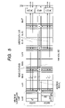
- FIG. 8 is a circuit diagram to explain a reading path from a memory mat.
- FIG. 9 is a circuit diagram to explain a writing path from a memory mat.
- FIGS. 10A and 10B are circuit diagrams to explain memory cell operations in a read cycle and a write cycle.
- FIG. 11 is a circuit diagram showing an embodiment of a read dummy bit section and an associated memory mat.
- FIG. 12 is a circuit diagram showing an embodiment of a write dummy bit section and an associated memory mat.
- FIG. 13 is a diagram depicting a layout of elements of a memory cell.
- FIG. 14 is a diagram depicting a layout of elements of one embodiment corresponding to the circuit diagram of FIG. 11 .
- FIG. 15 is a diagram depicting a layout of elements of one embodiment corresponding to the circuit diagram of FIG. 12 .
- FIG. 16 is a circuit diagram showing another embodiment of a write dummy bit section according to this invention.
- FIG. 17 is a circuit diagram showing yet another embodiment of a write dummy bit section according to this invention.
- FIGS. 18A and 18B are timing charts to explain a general operation of SRAM memory cells.
- FIGS. 19A and 19B are illustrative diagrams of an embodiment of a regular memory cell.
- FIGS. 20A and 20B are illustrative diagrams of an embodiment of a read dummy cell according to this invention.
- FIGS. 21A and 21B are illustrative diagrams of an embodiment of a write dummy cell according to this invention.
- FIG. 22 is a conceptual diagram of an example of application of SRAMs according to the present invention.
- FIG. 3 shows a whole block diagram of an embodiment of an SRAM according to this invention.
- a layout of blocks is shown corresponding to their actual geometrical arrangement on a semiconductor chip.
- the semiconductor chip is divided into four areas, as indicated by dotted lines in the figure, the division being made by an address input circuit region extending lengthwise in the horizontal center and an indirect logic region extending crosswise in the vertical center. Although not restrictive, these four areas each have identical memory arrays and address/data logic regions.
- One area is divided into two arrays (9M arrays) in right and left positions.
- One array has a storage capacity of about 9 Mbits and, therefore, the whole chip has a storage capacity of 72 Mbits (9 Mbits ⁇ 8).
- FIG. 4 shows a detailed block diagram of one array from FIG. 3 .
- One array (9M array) is divided into nine modules (1M modules) arranged in a lengthwise direction of FIG. 4 (also true for FIG. 2 ).
- Each module (1M module) is assigned two bit data input/output (I/O( 0 ), I/O( 1 ) through I/O( 16 ), I/O( 17 )).
- I/O( 0 ), I/O( 1 ) through I/O( 16 ), I/O( 17 ) To one of the four areas shown in FIG. 3 , two arrays (9M arrays) are allocated at both sides of an address/data bus logic region extending lengthwise in the horizontal center of the area. The address/data bus logic region selects one of the two arrays (9M arrays) at both sides thereof.
- the SRAM of this embodiment allows writing and reading of data of 2 ⁇ 9 bits in parallel to/from each array. If an operating mode in which four arrays are selected simultaneously is set or such setting is done with a memory select circuit, input and output of 72 bits of data can be performed. If an operating mode in which only one of the four arrays is selected is set or such setting is done with the memory select circuit, input and output of 18 bits of data can be performed.
- FIG. 5 shows a diagram depicting an arrangement of memory mats to explain one module (1M module) from FIG. 4 .
- the vertical and horizontal directions in FIG. 5 are opposite to those in FIG. 3 .
- a module (1M module) shown in FIG. 5 corresponds to one module in FIG. 4 rotated by 90 degrees.
- the module (1M module) is divided into two parts horizontally (vertically in FIG. 4 ).
- the module is further divided into memory blocks of BLK 0 to BLK 7 vertically (horizontally in FIG. 4 ).
- a memory block BLK 0 which is shown as exemplary one is divided, as mentioned above, into two memory mats MAT 00 , MAT 01 which are minimum controlled units.
- the above address/data bus logic region exists adjacently to a memory block BLK 7 and this region includes an address register AREG and data registers DREG 0 , 1 .
- AREG address register
- a write data bus carrying write signals and a read data bus carrying read signals extend, piercing through these mats.
- One memory mat e.g., MAT 00 is comprised of 264 word lines and 260 pairs of complementary bit lines.
- regular word lines are 256 lines and regular complementary bit lines are 256 pairs.
- the remaining word lines and complementary bit lines are intended for redundancy purposes and used for relief in case a fault occurred in the regular word lines and complementary bit lines.
- a write dummy bit section and a read dummy bit section are formed, utilizing a pair of complementary bit lines provided in each memory mat.
- FIG. 6 shows a diagram depicting an arrangement of memory mats to explain one module (1M module) from FIG. 4 in greater detail.
- the memory mats MAT 00 and MAT 01 which are shown as representative exemplary ones have word line select circuits SWD for selecting word lines WL. These word line select circuits SWD are installed such that they are adjacent to each other.
- a signal bus 9 including address signal lines extends between the memory mats MAT 00 and MAT 01 .
- a word line select circuit is comprised of: a decoding circuit that receives an address signal from the above address signal line through a control circuit which will be described later, decodes the address signal, and generates a signal for selecting one word line; and a word line driving circuit that amplifies that signal and drives the word line WL.
- a write dummy bit section is provided, utilizing a pair of complementary bit lines adjacent to the above address select circuit.
- a read dummy bit section is provided, utilizing a pair of complementary bit lines adjacent to the above address select circuit.
- the memory mats MAT 00 , MAT 01 and their adjacent memory mats MAT 10 , MAT 1 in the above memory block BLK 0 are combined in a set.
- column select circuits YSW, sense amplifiers SA, and write amplifiers WA are installed, which are responsible for the memory mats MAT 00 and MAT 10 , respectively.
- reference numeral 1 the memory mat MAT 00 and others are denoted by reference numeral 1 for consistency with further description.
- Reference numeral 3 denotes a timing control circuit CONT.
- Reference numeral 4 denotes each set of column select circuits YSW, sense amplifiers SA, and write amplifiers WA which are responsible for the memory mats, respectively.
- Reference numeral 5 denotes a write dummy bit section.
- Reference numeral 6 denotes a read dummy bit section.
- Reference numeral 7 denotes a memory cell (MC).
- Reference numeral 8 denotes a section including the above registers and drivers in the above address/data bus logic region.
- Reference numeral 9 denotes a signal bus including address signal lines.
- one memory mat per module is selected and conducted to the above registers and the like in the above address/data bus logic region. For this reason, it does not happen that select both memory mats such as MAT 00 , MAT 01 at the right and left sides of the address select circuit 2 are selected at the same time. Hence, allocating a write dummy bit section to one memory mat MAT 00 and allocating a read dummy bit section to the other memory mat MAT 01 will cause no problem. Accordingly, when the memory mat MAT 00 has been selected, the write dummy bit section in the memory mat MAT 00 and the read dummy bit section in the memory mat MAT 01 not selected can be used.
- the write dummy bit section and the read dummy bit section are placed adjacently to the address select circuit between adjacent mats and the timing control circuit is provided in the above mat circuit. Accordingly, the timing control circuit that controls the operations of the write dummy bit section and read dummy bit section can be formed to provide a common control of these sections and, moreover, wiring for connection is easy.
- the write dummy bit section or read dummy bit section of a memory mat not selected is used and, consequently, there are no dummy word lines which are used in the SRAM known from Patent Document 1.
- the read dummy bit section 6 one of a pair of complementary bit lines as mentioned above is used as a dummy bit line and the other is used as a dummy cell select line.
- the write dummy bit section one of a pair of the complementary bit lines as mentioned above is used as a dummy bit output line and the other is used as a dummy bit input line.
- dummy word lines are dispensed with and, therefore, e.g., dummy cells and select circuits coupled to these lines are dispensed with.
- This enables circuit simplification to a great extent in comparison with the configuration known from Patent Document 1 as mentioned before.
- the advantages of the invention of the present application i.e., the dummy word lines are dispensed with and only a dummy circuit using one complementary bit line is needed in one memory mat, produce a great difference in circuit scale of the whole memory chip.
- FIG. 7 shows a block diagram to explain a relationship between two memory mats and a control circuit from FIG. 6 .
- memory mats 1 MAT 00 and MAT 01
- a control circuit 3 CONT
- a word line of the memory mat 1 is selected by the address select circuit 2 .
- the address select circuit 2 (SWD+RDEC) is supplied with an X-coordinate address signal SXADDR via the control circuit 3 (CONT), decodes the address signal with an X-coordinate decoder RDEC, and generates a signal for selecting the word line WL in a word line driving circuit.
- Complementary bit lines BT, BB of the memory mat 1 (MAT 00 ) are selected by the column select circuit YSW included in the above circuit 4 (YSW/SA/WA).
- the column select circuit YSW is selected by a column decoder CDEC and makes the complementary bit lines BT, BB of the memory mat 1 (MAT 00 ) couple to an output terminal of the write amplifier WA or an input terminal of the sense amplifier SA.
- the column decoder CDEC is supplied with a Y-coordinate address signal SYADDR via the control circuit 3 (CONT), decodes the address signal, and generates a signal for selecting the above column select circuit YSW.
- the write amplifier WA is operated by a control signal DICMR and the sense amplifier SA is operated by a control signal RENMR.
- a data multiplexer DMAX selects and outputs a read signal amplified by the sense amplifier SA.
- the same circuits as described above are provided in the memory mat 1 (MAT 01 ) as well.
- the control circuit 3 receives an X-coordinate address signal AX which is used for selecting the above word line, a Y-coordinate address signal AY which is used for selecting the complementary bit lines, a mat select signal Mat, a block select signal BLK, a write control signal DIC, and a read control signal REN, and supplies the address signals as mentioned above to the above memory mat 1 (MAT 00 , MAT 01 ) and others and generates control signals for the write amplifier WA and the sense amplifier SA, an input signal WDMB to the write dummy bit section 5 , and a select signal TE to the read dummy bit section 6 .
- control circuit 3 When the above control circuit 3 (CONT) receives an output signal WDM in response to the above input signal WDMB from the write dummy bit section 5 , it terminates the write operation.
- a read operation when the above control circuit 3 (CONT) receives an output signal RDM in response to the above select signal TE from the read dummy bit section 6 , it terminates the read operation.
- the control unit deselects the selected word line of the above memory mat 1 (MAT 00 , MAT 01 ) and performs equalization of the complementary bit lines.
- FIG. 8 shows a circuit diagram to explain a reading path from the memory mat. This figure depicts a state where a word line WL 255 as a representative is selected and complementary bit lines BB 0 , BT 0 are selected by a column switch.
- a driver MOSFET QD 1 for one bit line BB is on and a driver MOSFET QD 2 for the other bit line BT is off.
- a p-channel load MOSFET QL 1 is off and a p-channel load MOSFET QL 2 is on.
- address selector MOSFETS QT 1 , QT 2 are turned on.
- a current path for discharging the precharged voltage of the bit line BB 0 is formed via the address selector MOSFET QT 1 made on by the above word line WL 255 , shown in FIG. 10A , and the above driver MOSFET QD 1 which is on.
- the bit line BT a current path for discharge is not formed, because the driver MOSFET QD 2 for the bit line BT is off, even though the address selector MOSFET QT 2 is on due to the voltage level of the selected word line WL 255 . Consequently, the complementary bit line BT remains at a high level of precharged voltage. Because the complementary bit line BB 0 is at a low level and BT 0 at a high level, as noted above, a voltage level difference appears at the input terminal of the sense amplifier SA via the column switch and it is amplified by the sense amplifier SA.
- FIG. 9 shows a circuit diagram to explain a writing path from the memory mat. This figure depicts a state where a word line WL 255 as a representative is selected and complementary bit lines BB 0 , BT 0 are selected by a column switch.
- the driver MOSFET QD 1 for one bit line BB is off and the driver MOSFET QD 2 for the other bit line BT is on.
- the p-channel load MOSFET QL 1 is on and the p-channel load MOSFET QL 2 is off.
- address selector MOSFETS QT 1 , QT 2 are turned on.
- FIG. 9 represents an example where writing is performed to invert the memory state of such a memory cell.
- the voltage level of the selected word line WL 255 makes the address selector MOSFET QT 1 shown in FIG. 10B on.
- column switch MOSFETs Q 5 , Q 6 are turned on by a column select signal YS 0 .
- a MOSFET Q 1 of the write amplifier WA When a MOSFET Q 1 of the write amplifier WA is turned on, a current path is formed for discharging a memory node formed by the drain of MOSFETs QD 1 , QL 1 coupled in common via the above column switch MOSFET Q 5 , the bit line BB, and the address selector MOSFET QT 1 in the memory cell and the gate of the driver MOSFET QD 2 .
- the driver MOSFET QD 1 for the bit line BB is off and the p-channel load MOSFET QL 1 is on in the memory cell shown in FIG. 10B . Due to this, a current flows from the above p-channel load MOSFET QL 1 to counteract the current for discharging the above node by a write current supplied by the above write amplifier WA. That is, the current acting to keep the memory state flows from the p-channel load MOSFET.
- the current flowing from the above p-channel MOSFET QL 1 is smaller than the current flowing through the MOSFET Q 1 of the above write amplifier WA, or causes the discharge of the voltage of the above memory node to a low level.
- This discharge triggers decreasing the gate voltage of the driver MOSFET QD 2 being on and increasing the gate voltage of the load MOSFET QL 2 accordingly.
- a positive feedback loop is produced in which the voltage of the driver MOSFET QD 1 being off increases to act to facilitate the voltage fall of the above memory node, which in turn decreases the current flowing through the above driver MOSFET QD 2 , and the gate voltage of the above driver MOSFET QD 1 is increased by the current flowing from the above load MOSFET QL 2 .
- the current from the bit line BT through the address selector MOSFET QT 2 acts to increase the gate voltage of the above driver MOSFET QD 1 in reverse proportion to a decrease in the current through the above driver MOSFET QD 2 .
- inversion occurs such that the driver MOSFET QD 1 becomes on and the load MOSFET QL 1 off, whereas the driver MOSFET QD 2 becomes off and the load MOSFET QL 2 on.
- FIG. 1 shows a circuit diagram of an embodiment of dummy bit sections and a control circuit according to this invention. Reference numerals used in this figure correspond to those in FIG. 7 .
- An input line for an input signal WDMB is formed by using wiring equivalent to one of the complementary bit lines of the memory mat MAT 00 , e.g., an inverting bit line BB.
- An output line for an output signal WDM is formed by using wiring equivalent to the other complementary bit line, a noninverting bit line BT.
- a source-drain path of a MOSFET equivalent to an n-channel address selector MOSFET QT 1 included in the memory cell shown in FIG. 10 is connected.
- the gate of this MOSFET QT 1 is constantly coupled to a supply voltage so that the MOSFET remains on.
- a MOSFET equivalent to a p-channel load MOSFET QL 1 included in the above memory cell is installed.
- MOSFETS QD 1 , QD 2 , QL 1 , QL 2 , QT 1 , and QT 2 included in the memory cell those equivalent to the above two MOSFETS QT 1 and QL 1 are selected and coupled to the above input line and output line.
- a feature of the invention disclosed in the present application is that the above MOSFETs as many as those used in a plurality of memory cells are coupled in the same way as described above. That is, MOSFETs equivalent to the above MOSFETs QT 1 , QL 1 as many as those used in the memory cells are, in parallel, coupled to the above input line and output line.
- a select line carrying a select signal TE is formed by using wiring equivalent to one of the complementary bit lines of the memory mat MAT 00 , e.g., an inverting bit line BB.
- An output line for an output signal RDM is formed by using wiring equivalent to the other complementary bit line, a noninverting bit line BT.
- MOSFETs equivalent to the above two MOSFETS QT 1 and QD 1 are selected and coupled to the above select line and output line.
- a feature of the invention disclosed in the present application is that the above MOSFETs as many as those used in the memory cells are coupled in the same way as described above. That is, the above MOSFETs as many as those used in the memory cells are, in parallel, coupled to the above select line and output line.
- An ordinary memory cell includes a plurality of cell transistors which are used for storing data and reading and writing.
- the cell transistors are coupled to another transistor among them, a supply voltage line, a ground line, a bit line, and a word line. Data cannot be written to the read and write dummy cells.
- These cells include the cell transistors used in an ordinary memory cell. How the transistors within a dummy cell are coupled each other differs from that in an ordinary memory cell.
- the shape of a dummy cell is similar to that of an ordinary cell. In most cases, the size of a dummy cell is usually the same as that of an ordinary cell. The same size is not always required, because the size may vary depending on cell boundary definition or the like. Because how the transistors in a dummy cell are coupled each other differs from that in an ordinary cell, different wiring and different shapes of connections and the like are often used in a dummy cell.
- p-channel precharge MOSFETs QP 1 , QP 2 for precharging the input line and output line of the above write dummy bit section 5 and a p-channel precharge MOSFET QP 3 for precharging the output line of the above read dummy bit section 6 are provided.
- the select line of the above read dummy bit section 6 is connected to a logic gate circuit G 2 that receives a read control signal REN and a block select signal BLK.
- This signal TE 0 is conveyed via a gate circuit G 5 onto the above select line TE.
- the gate circuit G 5 sets the above select signal TE in a selected state in relation to a test signal TEST also.
- a change in the output signal RDM through the above output line is detected by a detecting circuit comprised of two inverters chained and a detection signal RDM 0 is generated.
- This signal RDM 0 is conveyed to a gate circuit G 6 and a read word reset signal RPLS is generated.
- This signal RPLS becomes a reset signal RWPLS for the word line via a gate circuit G 9 .
- This signal RWPLS controls gate circuits G 12 , G 13 to stop the output of address signals SXADD[20:0], SYADD[15:0). Due to this, the selected word line is deselected.
- the input line of the above write dummy bit section 5 is connected to a logic gate circuit G 1 that receives a write control signal DIC and a block select signal BLK.
- a delay time in which a delay time in selecting a regular word line is taken into account is generated by an inverter chain DL 1 .
- a pulse RPLS corresponding to a write pulse is generated and an input signal WDMB is generated by driving a MOSFET N 1 analogous to the MOSFET in the write amplifier WA.
- reading is performed in the first half of one cycle of clock and writing is performed in the second half of the same cycle, as will be described later.
- the above read control signal REN is at a low level and the signal TE 0 is at a high level accordingly.
- RDM is turned to a high level through the read dummy bit section 6 and it is determined that reading has terminated by gate circuits G 6 , G 7 .
- an n-channel MOSFET QN 1 in relation to the write amplifier WA is turned on and the input line WDMB is turned to a low level.
- the low level of the input line WDMB is conveyed via MOSFETs in the above dummy bit section to the output line WMD. That is, current flows through the same current path as in writing to the memory cell as shown in FIG. 10B , a change to a low level on the output line WDM 0 in relation to the above memory node is detected by a detecting circuit comprised of two inverters chained, and a detection signal WDM 0 is generated.
- a gate circuit G 8 By taking this signal WDM 0 , a gate circuit G 8 generates a reset signal RWPLS for the write word line. This signal RWPLS becomes low level, after passing through a gate circuit G 9 . Again, the RWPLS signal controls the gate circuits G 12 , G 13 to stop the output of address signals SXADD[20:0], SYADD[15:0]. Due to this, the selected word line is deselected.
- Latch circuits FF 1 , FF 2 take in address signals AX, AY, responsive to the above RPLS. That is, upon detection of that the memory mat has been selected by the above MAT and BLK, the take-in of the address signals AX, AY is performed. Responsive to the above signal WPLS, a signal DICMR (see FIG. 7 ) that activates the write amplifier WA is generated by a gate circuit G 10 . Responsive to the above signal RPLS, a signal RENR (see FIG. 7 ) that activates the sense amplifier SA is generated by a gate circuit G 11 .
- FIG. 2 shows a waveform chart to explain the operations of the dummy bit sections and the control circuit in FIG. 1 .
- a read mode corresponds to a first half cycle in which clock RCC is low level and a write mode corresponds to a second half cycle in which clock RCC is high level.
- the read signal REN is turned to high level.
- the PRLS signal is turned to high level, the address signal AX/AY in relation to the selected memory mat is taken in, and AXL/AYL is generated.
- the RWPLS signal is turned to high level and the word line WL related to the taken-in address signal is selected.
- a read signal Bit Line appears in the complementary bit lines (BT, BB).
- the select signal TE (not shown) is conveyed to the read dummy bit section 6 .
- the RDM signal is output through the output line, RDM 0 is turned to low level, which turns the PRLS signal to low level.
- RWPLS is turned to low level, which resets the word line WL for reading to low level.
- equalization of the complementary bit lines is performed.
- the termination of reading is determined from the change to high level of the write signal DIC and the change to low level of the PRLS signal, and the WPLS signal is turned to high level.
- an address signal for writing is taken in and the word line WL for writing is selected.
- a write signal Bit Line is conveyed onto the complementary bit lines (BT, BB).
- the write signal is conveyed onto the input line of the write dummy bit section 5 and, in response to a write detection signal WDM 0 not shown, the WRLS signal is turned to low level. This turns RWPLS to low level and resets the word line WL for writing to low level.
- equalization of the complementary bit lines is performed. There is a cycle margin between the end of equalizing the complementary bit lines and the start of the next read cycle.
- each memory block includes the read dummy bit section and the write dummy bit section and the control circuit includes the latch circuits FF 1 , FF 2 for holding the read address signal longer, if the read pulse RPLS is longer than the low level period of the clock RCC.
- the pulse signal RPLS output from the read dummy bit section is input to the write dummy bit section to ensure that the write pulse WPLS just follows the read pulse RPLS, when reading and writing are continuously performed in the same memory array. According to this configuration, when reading and writing are performed continuously in the same memory array, it is possible to elongate the period of the read pulse RPLS, regardless of the duty of the external clock RCC, and read/write cycles at a higher rate can be achieved.
- the select signal TE for the read dummy bit section is input to the dummy bit section. Because the dummy bit section is configured in the same form of a memory cell and a path corresponding to the read current path is used, the RDM signal with a pulse width depending on the performance of the memory cell transistors is returned to the control circuit 3 .
- an address signal is converted to a pulse width RPLS returned from the read dummy bit section and input to the row decoder RDEC and the column decoder CDEC explained with FIG. 7 .
- the RDEC and CDEC decode each address signal into a word line select signal and a column select signal.
- the resulting word line select signal and column select signal can have the pulse width depending on the performance of the memory cell transistors, determined by the read dummy bit section.
- the output line RDM is pulled down to low level through the MOSFETs equivalent to access MOSFETs (QT) and driver MOSFETs (QD), included in the dummy bit section.
- a delay time from the change to high level of the signal TE until the change to low level of the output line RDM depends on the performance of the access MOSFETs (QT) and driver MOSFETs (QD).
- QT access MOSFETs
- QD driver MOSFETs
- the select signal PRLS for the read dummy bit section is input to the write dummy bit section.
- a signal WMD with a pulse width depending on the performance of the memory cell transistors is returned to the control circuit 3 and a write pulse WPLS is generated.
- the word line select signal and column select signal can have the pulse width WPLS depending on the performance of the memory cell transistors, determined by the write dummy bit section.
- the output line WDM is pulled down to low level through the access MOSFETs (QT) included in the write dummy bit section.
- a delay time until the change to low level of the output line WDM is determined by the percentage of load MOSFETs (QL) and access MOSFETs (QT) being on and this reflects the performance of the internal node in a regular bit memory cell in terms of time taken for inversion.
- the write dummy bit section employs the access MOSFETs and load MOSFETs as many as those used in a plurality of memory cells and the read dummy bit section employs the access MOSFETs and driver MOSFETs as many as those used in the memory cells.
- the detection signal is generated using such multiplied current. This produces an advantageous effect that a write pulse WPLS and a read pulse RPLS are generated from the above detection signal and, by using these pulses, it is possible to compensate a time delay until the word lines of regular memory cells are actually reset. That is, in advance of the operation of each memory cell, the detection signal reflecting the performance of the memory cell is generated and the word line of the memory cell is reset at nearly the same timing of the termination of the memory cell reading or writing.
- a write pulse WPLS and a read pulse RPLS are generated using the same current that flows in memory cells, the word line remains selected longer until the word line is reset using either of these pulses and this results in a bottleneck in high-speed access.
- Producing the multiplex current into which all currents flowing in the memory cells are combined has an advantageous effect that characteristic variations of the memory cells are absorbed. Even if, among the memory cells, there are some cells in which a large current flows and other cells in which only a small current flows, combining all currents flowing the memory cells into the multiplex current as above provides a possibility of obtaining an average memory cell current. That is, it is possible to generate a write pulse WPLS and a read pulse RPLS corresponding to an average performance of memory cells. A cell in which writing and reading cannot be performed by using such pulses WPLS and RPLS is rejected as a defective. If there is a cell in which writing or reading is impossible through a particular word line or bit line, such a defective memory cell should be replaced by a redundant circuit.
- timing adjustment only depends on the characteristic of one dummy element which may deviate from the average. Consequently, if timing adjustment is performed based on extremely short timing determined by the characteristic of the dummy element, most memory cells may be judged as errors even though they have no problem in their characteristics. Conversely, timing adjustment is performed based on extremely long timing determined by the characteristic of the dummy element, a problem that an error occurs when memory cells are operated in sync with an external clock with a short period may be encountered, even though they are normal as internal memory circuits.
- FIG. 11 shows a circuit diagram of an embodiment of a read dummy bit section and an associated memory mat.
- the number of dummy cells coupled to the output line RDM can be selected by select signals RDC 0 , RDC 1 , RDC 2 .
- This embodiment exemplifies that the number of dummy cells may be varied by the above select signals RDC 0 , RDC 1 , RDC 2 . This does not means that one dummy cell may only be used by selecting only one of the select signals RDC 0 , RDC 1 , RDC 2 .
- elements such as one related to the word line 255 , which are not used for generating the above read pulse RPLS, are coupled t the output line RDM so that the parasitic capacity of the output line RDM becomes equal to the parasitic capacity of the bit line BT or the like.
- MOSFETs provided to add a parasitic capacity, the gate of an n-channel MOSFET is coupled to the ground potential point, so that these MOSFETs remain off constantly.
- pattern dummies PD are provided near the word line select circuit SWD so that the elements included in the read dummy bit section 6 have the same pattern dependency as the elements included in regular memory cells MC.
- FIG. 12 shows a circuit diagram of an embodiment of a write dummy bit section and an associated memory mat.
- the number of dummy cells coupled to the output line WDM can be selected by select signals WDC 0 , WDC 1 , WDC 2 .
- This embodiment exemplifies that the number of dummy cells may be varied by the above select signals WDC 0 , WDC 1 , WDC 2 . This does not means that one dummy cell may only be used by selecting only one of the select signals WDC 0 , WDC 1 , WDC 2 .
- elements such as one related to the word line 255 , which are not used for generating the above write pulse WPLS, are coupled to the output line WDM so that the parasitic capacity of the output line WDM becomes equal to the parasitic capacity of the bit line BT or the like.
- MOSFETs provided to add a parasitic capacity, the gate of an n-channel MOSFET is coupled to the ground potential point, so that these MOSFETs remain off constantly.
- pattern dummies PD are provided near the word line select circuit SWD so that the elements included in the write dummy bit section 5 have the same pattern dependency as the elements included in regular memory cells MC
- a MOSFET QN 1 in FIG. 1 is comprised of a serial circuit of MOSFETs QN 1 ′ and QN 1 ′′.
- the MOSFET QN 1 ′ corresponds to the MOSFET Q 1 in the write amplifier in FIG. 9 and the MOSFET QN 1 ′′ corresponds to the MOSFET Q 5 in the column switch in FIG. 9 .
- the control circuit shown in FIG. 1 and others may include two MOSFETs QN 1 ′ and QN 1 ′′.
- FIG. 13 shows a diagram depicting a layout of elements of a memory cell. Zones surrounded by dotted lines are diffusion layers. On both sides of an area in which two P-channel MOSFETs (PMOS) are formed, there are areas in which two n-channel MOSFETs (NMOS) are formed.
- the driver MOSFET QD 1 and the load MOSFET QL 1 (QN 2 and QL 2 also) have a common gate electrode G.
- the driver MOSFET QD 1 and the address selector MOSFET QT 1 (QD 2 and QT 2 also) have a common source S diffusion layer and a common drain D. These common gate and diffusion layer are coupled by first layer wiring M 1 and a memory cell MC is formed.
- the other source and drain of the address selector MOSFET are coupled to the bit lines BB and BT not shown via the above wring layer M 1 and the gate thereof is coupled to the word line WL not shown via the above M 1 .
- the CON label in FIG. 13 denotes a contact coupling the diffusion layer and the wiring layer M 1 and a contact coupling the gate electrode layer and the wiring layer M 1 .
- the contacts are holes provided in an interlayer insulation film isolating upper layer wiring from lower layer wiring. The holes are filled with an electrically conductive material such as a metal and the like to couple the upper and lower layers.
- FIG. 14 is a diagram depicting a layout of elements of one embodiment corresponding to the circuit diagram of FIG. 11 .
- Memory cells like those shown in FIG. 13 are arranged vertically in FIG. 14 .
- This figure exemplifies the memory mats associated with word lines WL 0 to WL 2 .
- Dummy cells have diffusion layers and gate layers corresponding to those of the memory cells shown in FIG. 13 , wherein the first wiring M 1 pattern is changed such that a node coupling to the select line TE and a node coupling to the output line RDM are formed.
- These nodes are coupled to a wiring layer including complementary bit lines BB, BT extending crosswise in the figure and the select line TE and the output line RDM are formed.
- pattern dummies PD the diffusion layer, gate electrode, and wiring layer M 1 are formed in a pattern that is symmetrical to the pattern in regular memory cells.
- FIG. 15 is a diagram depicting a layout of elements of one embodiment corresponding to the circuit diagram of FIG. 12 .
- Memory cells like those shown in FIG. 13 are arranged vertically in FIG. 14 .
- This figure exemplifies the memory mats associated with word lines WL 0 to WL 2 .
- Dummy cells have diffusion layers and gate layers corresponding to those of the memory cells shown in FIG. 13 , wherein the first wiring M 1 pattern is changed such that a node coupling to the input line WDMB and a node coupling to the output line WDM are formed.
- These nodes are coupled to a wiring layer including complementary bit lines BB, BT extending crosswise in the figure and the input line WDMB and the output line WDM are formed.
- pattern dummies PD the diffusion layer, gate electrode, and wiring layer M 1 are formed in a pattern that is symmetrical to the pattern in regular memory cells.
- FIG. 16 shows a circuit diagram of another embodiment of a write dummy bit section according to this invention.
- the MOSFETs QT in relation to 18 memory cells are coupled to the input line WDMB.
- the MOSFETs QT in relation to the 18 memory cells and the MOSFETs QL are coupled to the output line WDM.
- the MOSFETs QT in relation to six memory cells can be added by a select signal WDMC 0 .
- Supply voltage VDD is applied to the gate of each p-channel MOSFET QL to make the MOSFET off constantly.
- the MOSFETs QT in relation to 16 memory cells can be added by a select signal WDMC 1 .
- the MOSFETs QT in relation to 24 memory cells can be added by a select signal WDMC 2 .
- the MOSFETs QT in relation to a maximum of 64 memory cells can be coupled to the input line WDMB and the output line WDM. That is, the select signals WDMC 2 to WDMC 0 and any combination thereof allows selection of any of the following: 18 (min.), 24, 34, 40, 42, 48, 58, and 64 (max.) MOSFETs QT.
- the elements in relation to remaining 200 memory cells coupled to the complementary bit lines are made off and coupled to the input line WDMB. Consequently, the input line WDMB is adopted to have the same parasitic capacity as that of the complementary bit line BB.
- FIG. 17 shows a circuit diagram of yet another embodiment of a write dummy bit section according to this embodiment.
- the MOSFETs QT in relation to 18 memory cells are coupled to the input line WDMB.
- the ground potential VSS of the circuit is supplied to the gates of these MOSFETs QL to make the MOSFETs off.
- Other parts of this embodiment are the same as illustrated in FIG. 15 . That is, the eight p-channel MOSFETs QL are made off for approximation to the inversion write conditions. In actual memory cells, the p-channel MOSFETs QL switch from on to off with the transition to the write state. However, in this embodiment, for simulation purposes, e.g., 10 MOSFETs are set off and 8 MOSFETs are set on for approximation to the inversion write conditions.
- the select signals WDMC 2 to WDMC 0 in FIGS. 16 and 17 are generated by, for example, selective fuse disconnection. Operation timing may be determined, once a memory chip has been formed on a wafer, and optimum pulses WPLS, RPLS for an individual chip may be selected by selectively disconnecting a fuse using a laser beam or the like. If a fuse can be disconnected electrically, the above pulse width can be set before the shipment of the SRAM. Alternately, an electrically programmable ROM may be adopted and the select signals WDMC 2 to WDMC 0 may be generated by electrical programming. The above description is also true for the read dummy bit section 6 .
- FIGS. 18A and 18B show timing charts to explain a general operation of SRAM memory cells.
- FIG. 18A represents read cycles.
- a word pulse width T 1 for read cycles should have a sufficient period in which the bit line signal reaches an amplitude that can be amplified by the sense amplifier properly. Because the amplitude of the bit line signal is small, the equalization time T 2 can be set short.
- FIG. 18B represents write cycles.
- the period in which the internal node of the memory cell is inverted is generally shorter than the period T 1 in which the bit line signal reaches an amplitude that can be amplified by the sense amplifier properly, and, hence, T 3 can be set shorter than T 1 .
- the bit line signal reaches its full amplitude.
- the bit line equalization time T 4 for write cycles should be longer than the bit line equalization time T 2 for read cycles.
- the time required for a read cycle T 1 +T 2 is longer than the time required for a write cycle T 3 +T 4 .
- memory cycle time can be set in the read dummy bit section, posing no problem with write cycles.
- memory cycle time should be set equivalent to the time required for a write operation. In this case, it will be expedient to set memory cycle time, using the write dummy bit section.
- a short write time as in the above example means that the data holding ability of memory cells is not high.
- memory cycle time may be determined by write dummy cells.
- FIGS. 19A and 19B show illustrative diagrams of an embodiment of a regular memory cell.
- FIG. 19A shows a circuit pattern and FIG. 19B shows interconnections of elements. Contacts C 1 to C 12 in FIG. 19A correspond to contacts C 1 to C 12 in FIG. 19B . Since FIG. 19A is the same as FIG. 13 , no further explanation is given.
- bold lines denote first layer metal wiring M 1 such as aluminum.
- FIGS. 20A and 20B show illustrative diagrams of an embodiment of a read dummy cell.
- FIG. 20A shows a circuit pattern and FIG. 20B shows interconnections of elements.
- connections by wiring M 1 differ from the connections in the regular memory cell in FIGS. 19A and 19B in the following respects.
- Contacts C 2 and C 3 are coupled by the wiring M 1 and the drain and source of the MOSFET QT 1 are coupled.
- Contacts C 3 and C 5 are not coupled, whereas contacts C 5 and C 6 are coupled and the drain and source of the MOSFET QL 1 are coupled.
- contacts C 8 and C 10 are not coupled, whereas contacts C 7 , C 8 , and C 9 are coupled and the source and drain of the MOSFET QL 2 are coupled to the ground line VSS, wherein the contact C 7 is not coupled to VDD in the upper layer.
- the contact C 10 is dispensed with. In this way, one read dummy cell as described above can be formed.
- FIGS. 21A and 21B show illustrative diagrams of an embodiment of a write dummy cell.
- FIG. 21A shows a circuit pattern and FIG. 21B shows interconnections of elements.
- the undercoat diffusion layer and gate electrode are the same as for the regular memory cell in FIGS. 19A and 19B , connections by wiring M 1 differ from the connections in the regular memory cell in FIGS. 19A and 19B in the following respects.
- Contacts C 3 and C 4 are coupled by the wiring M 1 and the source of the drain of the MOSFET QD 1 are coupled.
- contacts C 8 and C 10 are not coupled, contacts C 7 , C 8 , and C 9 are coupled and the source and drain of the MOSFET QL 2 are coupled to the ground line VSS, wherein the contact C 7 is not coupled to VDD in the upper layer.
- Contacts C 10 and C 11 are coupled by the wiring M 1 and the source and drain of the MOSFET QT 2 are coupled. In this way, one write dummy cell as described above can be formed.
- FIG. 22 shows a conceptual diagram of an example of application of SRAMs according to this invention.
- PCs which are personal computers in a branch office A are interconnected by LAN within each department A, B.
- LANs per department in the branch office A are interconnected via a router.
- Routers provided at branch offices A to C are interconnected via the Internet.
- SRAMs of the present embodiment are mounted in place in the above routers and used as relay memories for data transfer between the personal computers PCs.
- dummy cells are similar in shape to regular cells.
- regular cells usually have the same cell size as regular cells, it is not always required that dummy and regular cells have exactly the same dimensions and manufacturing error and the like are deservingly acceptable.
- a regular cell includes a plurality of cell transistors and a dummy cell includes several ones (all or part) of the cell transistors, wherein the interconnections of the transistors in the dummy cell differ from those in the regular cell.
- the arrangement of memory mats may be embodied in various forms.
- logic components that access the read dummy bit section and the write dummy bit section and generate a memory cell selection timing signal based on output signals from the above sections may be embodied in various forms.
- This invention can widely be used for semiconductor memory devices with static memory cells.
Landscapes
- Engineering & Computer Science (AREA)
- Microelectronics & Electronic Packaging (AREA)
- Computer Hardware Design (AREA)
- Static Random-Access Memory (AREA)
Abstract
Description
Claims (16)
Applications Claiming Priority (2)
| Application Number | Priority Date | Filing Date | Title |
|---|---|---|---|
| JP2007116379A JP5093885B2 (en) | 2007-04-26 | 2007-04-26 | Semiconductor memory device |
| JP2007-116379 | 2007-04-26 |
Publications (2)
| Publication Number | Publication Date |
|---|---|
| US20080266928A1 US20080266928A1 (en) | 2008-10-30 |
| US7656733B2 true US7656733B2 (en) | 2010-02-02 |
Family
ID=39886767
Family Applications (1)
| Application Number | Title | Priority Date | Filing Date |
|---|---|---|---|
| US12/059,220 Active 2028-07-23 US7656733B2 (en) | 2007-04-26 | 2008-03-31 | Semiconductor memory device |
Country Status (2)
| Country | Link |
|---|---|
| US (1) | US7656733B2 (en) |
| JP (1) | JP5093885B2 (en) |
Cited By (1)
| Publication number | Priority date | Publication date | Assignee | Title |
|---|---|---|---|---|
| US20090273994A1 (en) * | 2008-05-05 | 2009-11-05 | Meng-Fan Chang | Dual mode accessing signal control apparatus and dual mode timing signal generating apparatus |
Families Citing this family (10)
| Publication number | Priority date | Publication date | Assignee | Title |
|---|---|---|---|---|
| US9263384B2 (en) * | 2008-05-13 | 2016-02-16 | Infineon Technologies Ag | Programmable devices and methods of manufacture thereof |
| US7898875B2 (en) * | 2008-05-14 | 2011-03-01 | Taiwan Semiconductor Manufacturing Company, Ltd. | Write assist circuit for improving write margins of SRAM cells |
| TWI421880B (en) * | 2010-03-25 | 2014-01-01 | Faraday Tech Corp | Sram writing system and related apparatus |
| KR101080209B1 (en) * | 2010-09-30 | 2011-11-07 | 주식회사 하이닉스반도체 | Semiconductor devices |
| US9064561B2 (en) * | 2012-04-02 | 2015-06-23 | Arm Limited | Handling of write operations within a memory device |
| KR20150064950A (en) * | 2013-12-04 | 2015-06-12 | 에스케이하이닉스 주식회사 | Semiconductor memory device |
| JP6309258B2 (en) * | 2013-12-09 | 2018-04-11 | エイブリック株式会社 | Data reading device and semiconductor device |
| US10528515B2 (en) * | 2017-06-27 | 2020-01-07 | Intel Corporation | Memory channel driver with echo cancellation |
| US10867681B2 (en) * | 2018-03-23 | 2020-12-15 | Taiwan Semiconductor Manufacturing Company, Ltd. | SRAM memory having subarrays with common IO block |
| KR102366973B1 (en) | 2018-03-26 | 2022-02-24 | 삼성전자주식회사 | Memory device |
Citations (3)
| Publication number | Priority date | Publication date | Assignee | Title |
|---|---|---|---|---|
| JP2006004463A (en) | 2004-06-15 | 2006-01-05 | Matsushita Electric Ind Co Ltd | Semiconductor memory device |
| US20070280022A1 (en) * | 2006-06-01 | 2007-12-06 | Lam Van Nguyen | Method and Apparatus for a Dummy SRAM Cell |
| US20080112245A1 (en) * | 2006-10-25 | 2008-05-15 | Martin Ostermayr | Bit line dummy core-cell and method for producing a bit line dummy core-cell |
Family Cites Families (5)
| Publication number | Priority date | Publication date | Assignee | Title |
|---|---|---|---|---|
| JPH0660663A (en) * | 1992-08-07 | 1994-03-04 | Ricoh Co Ltd | Semiconductor memory device |
| JP3586856B2 (en) * | 1998-05-29 | 2004-11-10 | 株式会社ルネサステクノロジ | Semiconductor storage device |
| JP4031206B2 (en) * | 2001-02-19 | 2008-01-09 | 株式会社リコー | Semiconductor memory device |
| JP4408610B2 (en) * | 2002-08-09 | 2010-02-03 | 株式会社ルネサステクノロジ | Static semiconductor memory device |
| JP4405215B2 (en) * | 2002-09-12 | 2010-01-27 | パナソニック株式会社 | Memory device |
-
2007
- 2007-04-26 JP JP2007116379A patent/JP5093885B2/en active Active
-
2008
- 2008-03-31 US US12/059,220 patent/US7656733B2/en active Active
Patent Citations (3)
| Publication number | Priority date | Publication date | Assignee | Title |
|---|---|---|---|---|
| JP2006004463A (en) | 2004-06-15 | 2006-01-05 | Matsushita Electric Ind Co Ltd | Semiconductor memory device |
| US20070280022A1 (en) * | 2006-06-01 | 2007-12-06 | Lam Van Nguyen | Method and Apparatus for a Dummy SRAM Cell |
| US20080112245A1 (en) * | 2006-10-25 | 2008-05-15 | Martin Ostermayr | Bit line dummy core-cell and method for producing a bit line dummy core-cell |
Cited By (2)
| Publication number | Priority date | Publication date | Assignee | Title |
|---|---|---|---|---|
| US20090273994A1 (en) * | 2008-05-05 | 2009-11-05 | Meng-Fan Chang | Dual mode accessing signal control apparatus and dual mode timing signal generating apparatus |
| US7839706B2 (en) * | 2008-05-05 | 2010-11-23 | National Tsing Hua University | Dual mode accessing signal control apparatus and dual mode timing signal generating apparatus |
Also Published As
| Publication number | Publication date |
|---|---|
| JP2008276822A (en) | 2008-11-13 |
| JP5093885B2 (en) | 2012-12-12 |
| US20080266928A1 (en) | 2008-10-30 |
Similar Documents
| Publication | Publication Date | Title |
|---|---|---|
| US7656733B2 (en) | Semiconductor memory device | |
| KR101573509B1 (en) | Memory system with sectional data lines | |
| US6084818A (en) | Semiconductor memory device capable of efficient memory cell select operation with reduced element count | |
| US8023313B2 (en) | Resistance change memory device | |
| KR930003814B1 (en) | Semiconductor memory device | |
| US6954394B2 (en) | Integrated circuit and method for selecting a set of memory-cell-layer-dependent or temperature-dependent operating conditions | |
| US20080279033A1 (en) | Semiconductor integrated circuit device | |
| US7733734B2 (en) | Semiconductor memory device with control block sharing row decoders | |
| US9830996B2 (en) | Efuse bit cell, and read/write method thereof, and efuse array | |
| JP2010092580A (en) | Stacked memory device | |
| US6490210B2 (en) | Semiconductor memory integrated circuit employing a redundant circuit system for compensating for defectiveness | |
| US6366526B2 (en) | Static random access memory (SRAM) array central global decoder system and method | |
| KR102212814B1 (en) | Variable delay word line enable | |
| JP2010244615A (en) | Semiconductor device and write control method for semiconductor device | |
| US7457182B2 (en) | Semiconductor memory including self-timing circuit | |
| US5828622A (en) | Clocked sense amplifier with wordline tracking | |
| US9047936B2 (en) | Memory device having control circuitry for write tracking using feedback-based controller | |
| JP4007823B2 (en) | Semiconductor memory device | |
| KR102391131B1 (en) | Memory device with global and local latches | |
| US8824229B2 (en) | Semiconductor memory apparatus having a pre-discharging function, semiconductor integrated circuit having the same, and method for driving the same | |
| JP5311431B2 (en) | Semiconductor memory device | |
| US7502272B2 (en) | Self-timing read architecture for semiconductor memory and method for providing the same | |
| JP2000040395A (en) | Semiconductor storage device |
Legal Events
| Date | Code | Title | Description |
|---|---|---|---|
| AS | Assignment |
Owner name: RENESAS TECHNOLOGY CORP., JAPAN Free format text: ASSIGNMENT OF ASSIGNORS INTEREST;ASSIGNORS:SHINOZAKI, MASAO;SATO, HAJIME;REEL/FRAME:020747/0652 Effective date: 20080218 Owner name: RENESAS TECHNOLOGY CORP.,JAPAN Free format text: ASSIGNMENT OF ASSIGNORS INTEREST;ASSIGNORS:SHINOZAKI, MASAO;SATO, HAJIME;REEL/FRAME:020747/0652 Effective date: 20080218 |
|
| FEPP | Fee payment procedure |
Free format text: PAYOR NUMBER ASSIGNED (ORIGINAL EVENT CODE: ASPN); ENTITY STATUS OF PATENT OWNER: LARGE ENTITY |
|
| STCF | Information on status: patent grant |
Free format text: PATENTED CASE |
|
| AS | Assignment |
Owner name: NEC ELECTRONICS CORPORATION, JAPAN Free format text: MERGER;ASSIGNOR:RENESAS TECHNOLOGY CORP.;REEL/FRAME:024879/0190 Effective date: 20100401 Owner name: RENESAS ELECTRONICS CORPORATION, JAPAN Free format text: CHANGE OF NAME;ASSIGNOR:NEC ELECTRONICS CORPORATION;REEL/FRAME:024864/0635 Effective date: 20100401 |
|
| FPAY | Fee payment |
Year of fee payment: 4 |
|
| FPAY | Fee payment |
Year of fee payment: 8 |
|
| AS | Assignment |
Owner name: RENESAS ELECTRONICS CORPORATION, JAPAN Free format text: CHANGE OF ADDRESS;ASSIGNOR:RENESAS ELECTRONICS CORPORATION;REEL/FRAME:044928/0001 Effective date: 20150806 |
|
| MAFP | Maintenance fee payment |
Free format text: PAYMENT OF MAINTENANCE FEE, 12TH YEAR, LARGE ENTITY (ORIGINAL EVENT CODE: M1553); ENTITY STATUS OF PATENT OWNER: LARGE ENTITY Year of fee payment: 12 |