JP2010020863A - Three dimensional memory device - Google Patents
Three dimensional memory device Download PDFInfo
- Publication number
- JP2010020863A JP2010020863A JP2008182410A JP2008182410A JP2010020863A JP 2010020863 A JP2010020863 A JP 2010020863A JP 2008182410 A JP2008182410 A JP 2008182410A JP 2008182410 A JP2008182410 A JP 2008182410A JP 2010020863 A JP2010020863 A JP 2010020863A
- Authority
- JP
- Japan
- Prior art keywords
- word line
- groups
- mat
- cell
- bit
- Prior art date
- Legal status (The legal status is an assumption and is not a legal conclusion. Google has not performed a legal analysis and makes no representation as to the accuracy of the status listed.)
- Granted
Links
- 239000011159 matrix material Substances 0.000 claims abstract description 7
- 239000000758 substrate Substances 0.000 claims description 12
- 239000004065 semiconductor Substances 0.000 claims description 6
- 239000010410 layer Substances 0.000 description 50
- 230000002950 deficient Effects 0.000 description 37
- 238000003491 array Methods 0.000 description 13
- 238000000034 method Methods 0.000 description 13
- 230000015556 catabolic process Effects 0.000 description 9
- 238000007667 floating Methods 0.000 description 9
- 101001070329 Geobacillus stearothermophilus 50S ribosomal protein L18 Proteins 0.000 description 8
- 230000000694 effects Effects 0.000 description 8
- 230000007274 generation of a signal involved in cell-cell signaling Effects 0.000 description 6
- 230000004913 activation Effects 0.000 description 5
- 230000000295 complement effect Effects 0.000 description 5
- 230000008859 change Effects 0.000 description 4
- 230000007547 defect Effects 0.000 description 4
- 238000001514 detection method Methods 0.000 description 4
- 230000007257 malfunction Effects 0.000 description 3
- 238000010586 diagram Methods 0.000 description 2
- 230000006870 function Effects 0.000 description 2
- 230000008569 process Effects 0.000 description 2
- 238000010187 selection method Methods 0.000 description 2
- 230000006641 stabilisation Effects 0.000 description 2
- 238000011105 stabilization Methods 0.000 description 2
- 230000007704 transition Effects 0.000 description 2
- 101000575029 Bacillus subtilis (strain 168) 50S ribosomal protein L11 Proteins 0.000 description 1
- 101000592939 Bacillus subtilis (strain 168) 50S ribosomal protein L24 Proteins 0.000 description 1
- 102100035793 CD83 antigen Human genes 0.000 description 1
- 101150110971 CIN7 gene Proteins 0.000 description 1
- 101100286980 Daucus carota INV2 gene Proteins 0.000 description 1
- 101000946856 Homo sapiens CD83 antigen Proteins 0.000 description 1
- 101150110298 INV1 gene Proteins 0.000 description 1
- 101100397044 Xenopus laevis invs-a gene Proteins 0.000 description 1
- 101100397045 Xenopus laevis invs-b gene Proteins 0.000 description 1
- 230000003213 activating effect Effects 0.000 description 1
- 239000012141 concentrate Substances 0.000 description 1
- 238000006880 cross-coupling reaction Methods 0.000 description 1
- 230000003292 diminished effect Effects 0.000 description 1
- 238000005516 engineering process Methods 0.000 description 1
- 239000011229 interlayer Substances 0.000 description 1
- 238000012544 monitoring process Methods 0.000 description 1
- 230000004044 response Effects 0.000 description 1
- 239000000126 substance Substances 0.000 description 1
Images


Classifications
-
- G—PHYSICS
- G11—INFORMATION STORAGE
- G11C—STATIC STORES
- G11C5/00—Details of stores covered by group G11C11/00
- G11C5/02—Disposition of storage elements, e.g. in the form of a matrix array
-
- G—PHYSICS
- G11—INFORMATION STORAGE
- G11C—STATIC STORES
- G11C29/00—Checking stores for correct operation ; Subsequent repair; Testing stores during standby or offline operation
- G11C29/04—Detection or location of defective memory elements, e.g. cell constructio details, timing of test signals
- G11C29/50—Marginal testing, e.g. race, voltage or current testing
-
- G—PHYSICS
- G11—INFORMATION STORAGE
- G11C—STATIC STORES
- G11C29/00—Checking stores for correct operation ; Subsequent repair; Testing stores during standby or offline operation
- G11C29/70—Masking faults in memories by using spares or by reconfiguring
- G11C29/78—Masking faults in memories by using spares or by reconfiguring using programmable devices
- G11C29/83—Masking faults in memories by using spares or by reconfiguring using programmable devices with reduced power consumption
- G11C29/832—Masking faults in memories by using spares or by reconfiguring using programmable devices with reduced power consumption with disconnection of faulty elements
-
- G—PHYSICS
- G11—INFORMATION STORAGE
- G11C—STATIC STORES
- G11C5/00—Details of stores covered by group G11C11/00
- G11C5/02—Disposition of storage elements, e.g. in the form of a matrix array
- G11C5/025—Geometric lay-out considerations of storage- and peripheral-blocks in a semiconductor storage device
-
- G—PHYSICS
- G11—INFORMATION STORAGE
- G11C—STATIC STORES
- G11C5/00—Details of stores covered by group G11C11/00
- G11C5/06—Arrangements for interconnecting storage elements electrically, e.g. by wiring
- G11C5/066—Means for reducing external access-lines for a semiconductor memory clip, e.g. by multiplexing at least address and data signals
-
- G—PHYSICS
- G11—INFORMATION STORAGE
- G11C—STATIC STORES
- G11C8/00—Arrangements for selecting an address in a digital store
- G11C8/12—Group selection circuits, e.g. for memory block selection, chip selection, array selection
-
- G—PHYSICS
- G11—INFORMATION STORAGE
- G11C—STATIC STORES
- G11C8/00—Arrangements for selecting an address in a digital store
- G11C8/14—Word line organisation; Word line lay-out
-
- G—PHYSICS
- G11—INFORMATION STORAGE
- G11C—STATIC STORES
- G11C29/00—Checking stores for correct operation ; Subsequent repair; Testing stores during standby or offline operation
- G11C29/04—Detection or location of defective memory elements, e.g. cell constructio details, timing of test signals
- G11C2029/0409—Online test
-
- G—PHYSICS
- G11—INFORMATION STORAGE
- G11C—STATIC STORES
- G11C29/00—Checking stores for correct operation ; Subsequent repair; Testing stores during standby or offline operation
- G11C29/04—Detection or location of defective memory elements, e.g. cell constructio details, timing of test signals
- G11C29/50—Marginal testing, e.g. race, voltage or current testing
- G11C2029/5006—Current
Landscapes
- Engineering & Computer Science (AREA)
- Microelectronics & Electronic Packaging (AREA)
- Semiconductor Memories (AREA)
Abstract
Description
この発明は、セルアレイが三次元的に配列されたメモリデバイスに係り、特に不良セルの影響を低減するセルアレイ層の選択法に関する。 The present invention relates to a memory device in which cell arrays are arranged three-dimensionally, and more particularly to a method of selecting a cell array layer that reduces the influence of defective cells.
最近、電圧、電流や熱などで物質の抵抗状態を変えて、その抵抗状態をデータとして利用する抵抗変化メモリ(Resistance RAM;ReRAM)がNAND型フラッシュメモリの後続候補として注目されている(例えば、非特許文献1参照)。抵抗変化メモリは微細化に向いていると同時に、クロスポイントセルを構成できる上に積層化が容易であり、大容量ファイルメモリとして利用価値が高いと考えられる。 Recently, a resistance change memory (Resistance RAM; ReRAM) that changes the resistance state of a substance by voltage, current, heat, or the like and uses the resistance state as data has attracted attention as a subsequent candidate of a NAND flash memory (for example, Non-patent document 1). The resistance change memory is suitable for miniaturization, and at the same time, can form a cross-point cell and can be easily stacked, and is considered to be highly useful as a large capacity file memory.
しかし、多数のセルアレイの積層化を可能にするためには、選択されるメモリセルが属する層の選択方式が重要となる。その理由は、セルアレイがクロスポイントセルアレイとして構成されて、層間でセルを選択する信号配線(クセス信号線やデータ線)が共有されることが多く、不良セルのリーク電流の影響が各層にまたがって生じる可能性があるからである。リーク電流の影響が広範囲にわたると、誤動作やパワーの増大を招き、多層構成での折角の大容量化もその効果が減殺されるおそれがある。 However, in order to enable a large number of cell arrays to be stacked, a method for selecting a layer to which a selected memory cell belongs is important. The reason for this is that the cell array is configured as a cross-point cell array, and signal wiring (access signal lines and data lines) for selecting cells is often shared between layers, and the influence of the leakage current of defective cells spans each layer. This is because it may occur. If the influence of the leakage current is wide, a malfunction and an increase in power are caused, and the effect of increasing the folding capacity in the multilayer structure may be diminished.
また積層されたセルアレイ層からの配線を下地基板の回路部に接続する部分の構成を簡単にするためには、層間の信号配線の共有化が重要となるが、不良セルの影響範囲の限定を、この信号配線の共有化との関係で最適化することが必要となる。
この発明は、不良セルの影響を低減できる層選択方式を適用した三次元メモリデバイスを提供することを目的とする。 It is an object of the present invention to provide a three-dimensional memory device to which a layer selection method that can reduce the influence of defective cells is applied.
この発明の一態様による三次元メモリデバイスは、メモリセルが二次元マトリクス状に配列されたマットを複数層積層して構成され、各マット内でメモリセル選択を行うアクセス信号線とデータ線とがそれぞれ隣接マット間で共有された三次元メモリデバイスであって、
積層されたマットが3つ以上の複数グループに分けられ、その複数グループの一つが選択されるときに、残りのグループの一部においてメモリセルがリーク電流の流れる状態にバイアスされ、残部においてメモリセルがリーク電流の流れない状態にバイアスされることを特徴とする。
A three-dimensional memory device according to an aspect of the present invention is configured by stacking a plurality of mats in which memory cells are arranged in a two-dimensional matrix, and an access signal line and a data line for selecting a memory cell in each mat. Each of which is a 3D memory device shared between adjacent mats,
When the stacked mats are divided into three or more groups and one of the groups is selected, the memory cells are biased in a state where a leakage current flows in a part of the remaining groups, and the memory cells in the remaining part Is biased to a state where no leakage current flows.
この発明の他の態様による三次元メモリデバイスは、
半導体基板と、
前記半導体基板上にメモリセルが二次元マトリクス状に配列されたマットを複数層積層して構成され、各マット内でメモリセル選択を行うアクセス信号線とデータ線とがそれぞれ隣接マット間で共有された三次元セルアレイと、
前記半導体基板の前記三次元セルアレイ下に形成されて、前記三次元セルアレイの読み出し及び書き込み制御を行う制御回路とを備え、
前記制御回路は、前記三次元セルアレイのマットを3つ以上の複数グループに分けて、その複数グループの一つを選択するときに、残りのグループの一部を同時に選択し、残部を非選択とするグループ選択回路を有する
ことを特徴とする。
A three-dimensional memory device according to another aspect of the present invention provides:
A semiconductor substrate;
A plurality of mats in which memory cells are arranged in a two-dimensional matrix are stacked on the semiconductor substrate, and access signal lines and data lines for selecting memory cells in each mat are shared between adjacent mats. A three-dimensional cell array,
A control circuit that is formed under the three-dimensional cell array of the semiconductor substrate and controls reading and writing of the three-dimensional cell array;
The control circuit divides the mat of the three-dimensional cell array into three or more groups, and when selecting one of the groups, selects a part of the remaining groups at the same time, and selects the rest as unselected. And a group selection circuit.
この発明によれば、不良セルの影響を低減できる層選択方式を適用した三次元メモリデバイスを提供することができる。 According to the present invention, it is possible to provide a three-dimensional memory device to which a layer selection method that can reduce the influence of defective cells is applied.
以下、この発明の実施の形態を説明する。 Embodiments of the present invention will be described below.
[ReRAM構成概要]
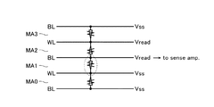
図1は、実施の形態による三次元(3D)セルアレイ構造のReRAMについて、その3Dセルアレイブロック1と下地制御回路2の構成概要を示している。ここでは、セルアレイブロック1は、説明を簡単にするため、4層のセルアレイMA0〜MA3が積層された例を示している。
[ReRAM configuration overview]
FIG. 1 shows a schematic configuration of a 3D
ワード線WL及びビット線BLは、隣接セルアレイ間で共有する方式とする。 各セルアレイ層のワード線WLは、そのワード線方向(y方向)の両端で、交互に垂直配線31により、下地の制御回路2に接続される。ビット線BLは、ビット線方向(x方向)の両側から交互に出て、3Dセルアレイ層の下から数えて偶数番目層と奇数番目層がそれぞれ層間では共通接続されて、下地制御回路2に接続される。即ちセルアレイブロック1の4辺を全てワード線WLとビット線BLの垂直配線31,32の領域としている。なおビット線について偶奇の各層間を共通接続しない方法もあり、以下の実施の形態ではこの共通接続のない場合を説明する。
The word line WL and the bit line BL are shared between adjacent cell arrays. The word lines WL in each cell array layer are connected to the
制御回路2は、主な回路配置例を図に示した。セルアレイのビット線方向両端で垂直配線32により基板上に降りたビット線は、マルチプレクサ(MUX)24a,24bで選択されて、アレイバス23a,23b上の信号が得られる。このバス上の信号はセンスアンプ回路22a,22bに入力される。センスアンプ回路22a,22bと外部とのデータのやり取りはデータバス21a,21bを介して行なわれる。
The
ワード線方向ではセルアレイの両端で垂直配線31により基板上に降りたワード線はワード線デコーダ/マルチプレクサ25a,25bに入る。外部とのデータやり取りを考慮したバス領域の設定として、この例ではワード線デコーダ/マルチプレクサ25a,25bとセルアレイブロック1の間に隙間を空けて一部のデータバス21bをこの隙間に配置する。
In the word line direction, the word lines descending on the substrate by the
セルアレイブロック1の直下のデータバス21aの領域は、その配線領域に直交する、セルアレイブロック1のワード線端の両辺に沿ってのデータバス21bに2分されセルアレイブロック1の直下領域から外部に出ていく。
The area of the
図2は、各層セルアレイの等価回路を示している。ワード線WLとビット線BLの各クロスポイントに、可変抵抗素子VRとダイオードDiを直列接続したメモリセルMCが配置される。図3は、各層セルアレイMA0−MA3の隣接するセルアレイ間で、メモリセルのダイオード極性を逆極性にすることを示している。 FIG. 2 shows an equivalent circuit of each layer cell array. At each cross point of the word line WL and the bit line BL, a memory cell MC in which a variable resistance element VR and a diode Di are connected in series is arranged. FIG. 3 shows that the diode polarity of the memory cell is reversed between adjacent cell arrays of each of the layer cell arrays MA0 to MA3.
例えばデータ読み出し時は、選択ワード線をVssとして、選択ビット線にVreadを与え、非選択ワード線をVread、非選択ビット線をVssとして、選択されたセルアレイの選択セルのデータをセンスアンプで読むことができる。 For example, when data is read, the selected word line is set to Vss, Vread is applied to the selected bit line, the unselected word line is set to Vread, and the unselected bit line is set to Vss, and the data of the selected cell of the selected cell array is read by the sense amplifier. be able to.
選択セルを高抵抗状態(リセット状態)から低抵抗状態(セット状態)に設定するには、選択ワード線をVss、選択ビット線をVpとし、選択セルに書き込みに必要な電圧Vp−Vssを所定のパルス幅で与える。これにより、選択セルの可変抵抗素子を電圧過程により低抵抗状態にすることができる(セット動作)。 To set the selected cell from the high resistance state (reset state) to the low resistance state (set state), the selected word line is set to Vss, the selected bit line is set to Vp, and the voltage Vp−Vss required for writing to the selected cell is predetermined. Is given by the pulse width. Thus, the variable resistance element of the selected cell can be brought into a low resistance state by a voltage process (set operation).
選択セルを低抵抗状態から高抵抗状態に設定するには、セット時とは異なる電圧(或いは同じ電圧)、異なるパルス幅で選択セルにリセット用電圧を与えて、素子が発生するジュール熱による熱過程を利用する(リセット動作)。 To set the selected cell from the low resistance state to the high resistance state, a reset voltage is applied to the selected cell with a voltage (or the same voltage) different from that at the time of setting and a different pulse width, and the heat generated by the Joule heat generated by the element. Use the process (reset operation).
なおここでのワード線WLとビット線BLの役割は便宜的なもので、いずれをワード線と呼ぶかはシステムの状況による。 Note that the roles of the word line WL and the bit line BL here are convenient, and which one is called a word line depends on the situation of the system.
以上のような3DセルアレイのReRAMにおいて、この実施の形態では、3Dセルアレイを3つ以上の複数グループに分けて、選択的にその一部のグループを非活性にしておくことにより、不良セルのリーク電流の影響を軽減する。 In the ReRAM having the 3D cell array as described above, in this embodiment, the 3D cell array is divided into three or more groups, and some of the groups are selectively deactivated, thereby causing a leak of defective cells. Reduce the effect of current.
[実施の形態の技術要素概要]
実施の形態の技術的要素をまとめると、次の通りである。
[Technical element overview of the embodiment]
The technical elements of the embodiment are summarized as follows.
(1)メモリセルが二次元マトリクス状に配列されたセルアレイ(以下、これをマットと称することがある)を複数層積層した3Dメモリデバイスにおいて、各層間で共有される、メモリセル選択のためのアクセス信号/データ線を3つ以上の複数グループに分け、その複数グループのうちの一部のグループにおいて、アクセス信号/データ線の多くが、アクセス信号線とデータ線間のメモリセルのセル電流を発生させる電位差より小さな電位差の範囲に設定されるようにする。 (1) In a 3D memory device in which a plurality of cell arrays in which memory cells are arranged in a two-dimensional matrix (hereinafter sometimes referred to as a mat) are stacked, a memory cell selection shared between the layers is used. The access signal / data line is divided into three or more groups, and in some of the groups, many of the access signal / data lines have a cell current of the memory cell between the access signal line and the data line. The potential difference is set to be smaller than the potential difference to be generated.
(2)同様の3Dメモリデバイスにおいて、アクセス信号線/データ線を3つ以上の複数グループに分け、その複数グループ内の一部グループのみにおいて、アクセス信号線とデータ線間のメモリセルにセル電流を発生させる電位差以上の電位差が与えられるようにする。 (2) In the same 3D memory device, the access signal line / data line is divided into three or more groups, and only in some of the groups, the cell current is supplied to the memory cell between the access signal line and the data line. A potential difference equal to or greater than the potential difference for generating the voltage is given.
(3)メモリセルは、一定以上の電圧または電流を印加して抵抗値を変化させる可変抵抗素子とダイオードとの直列接続として構成され、単位セルアレイはアクセス信号線(ワード線WL)とデータ線(ビット線BL)との間にメモリセルが配置されるクロスポイントセルアレイとして構成される。アクセス信号線とデータ線をそれぞれセルアレイ間で共有して、複数セルアレイが積層され、データ線のセル電流をモニタしてセル状態を判定するように、3DセルアレイのReRAMが構成される。 (3) The memory cell is configured as a series connection of a variable resistance element that changes a resistance value by applying a voltage or current of a certain level or more and a diode, and the unit cell array has an access signal line (word line WL) and a data line ( Bit line BL) is configured as a cross-point cell array in which memory cells are arranged. The access signal line and the data line are shared between the cell arrays, a plurality of cell arrays are stacked, and the ReRAM of the 3D cell array is configured to determine the cell state by monitoring the cell current of the data line.
このようなReRAMにおいて、アクセス信号線を層選択に関して3つ以上の複数グループに分けて層間でグループごとにアクセス信号線を共用し、選択メモリセルを含むセルアレイのアクセス信号線とデータ線以外のアクセス信号線とデータ線の電位が、メモリセルのダイオードが逆バイアスになるように設定される。 In such a ReRAM, the access signal lines are divided into a plurality of groups of three or more for layer selection, and the access signal lines are shared for each group between the layers, and access other than the access signal lines and data lines of the cell array including the selected memory cell is accessed. The potential of the signal line and the data line is set so that the diode of the memory cell is reverse biased.
(4)メモリセルが二次元マトリクス状に配列されたマットを複数積層した3Dメモリデバイスにおいて、メモリセル選択のためのアクセス信号線/データ線を3つ以上の複数グループに分け、非選択アクセス信号線に同じ電位を与えるグループを選択するために、選択メモリセルが属するマットを識別するアドレスビットから同じ電位を与えるグループを選択する信号を発生する回路が、アドレスビットに対する加算回路を用いて構成される。 (4) In a 3D memory device in which a plurality of mats in which memory cells are arranged in a two-dimensional matrix are stacked, access signal lines / data lines for selecting memory cells are divided into three or more groups and non-selected access signals In order to select a group that applies the same potential to the line, a circuit that generates a signal that selects a group that applies the same potential from the address bits that identify the mat to which the selected memory cell belongs is configured using an adder circuit for the address bits. The
(5)メインワード線を選択し、メインワード線によって選ばれた複数の部分ワード線ドライバ回路に選択信号を選択的に供給してアクセス信号線の電位が設定されるダブルワード線スキームの3Dメモリデバイスにおいて、アクセス信号線のグループごとに部分ワード線ドライバ回路を持ち、グループを選択する信号の活性化状態の組合せによってアクセス信号線の電流パスを切り替える回路を備える。 (5) A 3D memory having a double word line scheme in which a main word line is selected and a selection signal is selectively supplied to a plurality of partial word line driver circuits selected by the main word line to set an access signal line potential. The device includes a partial word line driver circuit for each group of access signal lines, and a circuit that switches a current path of the access signal line depending on a combination of activation states of signals for selecting the group.
(6)メインワード線を選択し、メインワード線によって選ばれた複数の部分ワード線ドライバ回路に選択信号を選択的に供給してアクセス信号線の電位が設定されるダブルワード線スキームの3Dメモリデバイスにおいて、アクセス信号線のグループごとに部分ワード線ドライバ回路を持ち、グループ分けされた層のアクセス信号線が、グループ層ごとに層間で共通接続されて、基板上の部分ワード線ドライバ回路の出力部へと接続される。 (6) 3D memory of a double word line scheme in which a main word line is selected and a selection signal is selectively supplied to a plurality of partial word line driver circuits selected by the main word line to set the potential of the access signal line The device has a partial word line driver circuit for each group of access signal lines, and the access signal lines of the grouped layers are commonly connected between the layers for each group layer, and the output of the partial word line driver circuit on the substrate Connected to the department.
[リーク電流の影響]
具体的な実施の形態の説明に先立って、先ず図4を参照して、ビット線BLとワード線WLをそれぞれ隣接セルアレイ間で共有する方式とした3D−ReRAMにおけるリーク電流の影響、具体的に選択セルについて、どれだけ離れたマットの不良セルの影響が現れるかを検討する。
[Effect of leakage current]
Prior to the description of a specific embodiment, first, referring to FIG. 4, the influence of leakage current in a 3D-ReRAM in which a bit line BL and a word line WL are shared between adjacent cell arrays, specifically, Consider how far away the defective cell of the mat appears for the selected cell.
図4には、7層のセルアレイMA0−MA6の範囲について、太線で示すワード線WL32とビット線BL22によりセルSCが選択されたときの不良セルDC1〜DC6のリークの影響を示している。 FIG. 4 shows the influence of leakage of defective cells DC1 to DC6 when the cell SC is selected by the word line WL32 and the bit line BL22 indicated by bold lines in the range of the seven-layer cell arrays MA0 to MA6.
セル選択はそのセルをクロスポイントとするワード線WLを接地電圧Vssに設定し、ビット線BLに動作モードに応じた電圧を与えて、ビット線BLに流れ込む電流を制御することによって行なう。図4の例は読み出し動作時であり、選択ビット線BL22は、電源電圧Vddより低い読み出し用電圧とする。 Cell selection is performed by setting the word line WL having the cell as a cross point to the ground voltage Vss, applying a voltage according to the operation mode to the bit line BL, and controlling the current flowing into the bit line BL. The example of FIG. 4 is during a read operation, and the selected bit line BL22 is set to a read voltage lower than the power supply voltage Vdd.
非選択ワード線WLは高い電圧例えばVd*(ビット線BLにかける最高電圧Vddよりダイオードの順方向電圧降下分Vf程度低い電圧)を印加し、非選択ビット線BLにはVs*(ビット線BLにかける最低電圧VssよりダイオードのVf 程度高い電圧)を設定してダイオードに順方向電流が流れないようにする。 A non-selected word line WL is applied with a high voltage, for example, Vd * (a voltage lower by about the diode forward voltage drop Vf than the maximum voltage Vdd applied to the bit line BL), and Vs * (bit line BL) is applied to the unselected bit line BL. Is set to prevent the forward current from flowing through the diode.
なお、非選択ビット線はフローティングでも動作期間に実質的にVs*となる電位であればよい。また、ダイオードの逆耐圧特性が悪いため不良と見なされるリーク電流の大きな不良セルが属するビット線BLは予め検出されて、フローティングに設定されるものとする。 It should be noted that the non-selected bit line may be a floating potential as long as it is substantially at Vs * during the operation period. In addition, it is assumed that the bit line BL to which a defective cell having a large leakage current that is regarded as defective because the reverse breakdown voltage characteristic of the diode is poor is detected in advance and set to be floating.
図4の例は、7層マットからなる真中の層MA3でセルSCを選択して読み出す場合であり、その2層目MA1から6層目MA6にそれぞれ逆バイアスリークの大きな不良セルDC1(MA1),DC2(MA2),DC3(MA3),DC4(MA4),DC5(MA5),DC6(MA6)がある例を示している。 The example of FIG. 4 shows a case where the cell SC is selected and read in the middle layer MA3 composed of a seven-layer mat, and the defective cell DC1 (MA1) having a large reverse bias leak from the second layer MA1 to the sixth layer MA6. , DC2 (MA2), DC3 (MA3), DC4 (MA4), DC5 (MA5), and DC6 (MA6) are shown.
真中の層マットMA3で選択されるセルSCは、不良セルとはビット線とワード線を共有しないものとして、選択ワード線WL32にはVss、選択ビット線BL22はVddよりかなり低い電位レベルがかけられる。 The cell SC selected by the middle layer mat MA3 is applied with a potential level considerably lower than Vdd on the selected word line WL32 and the selected bit line BL22 on the assumption that the defective cell does not share the bit line and the word line. .
不良セルにつながるビット線(不良ビット線)はフローティングにされる。従って、図のように不良セルDC2,DC4,DC3,DC5を流れるリーク電流Idが流れて、選択ワード線にまで流れ込むパスがあるビット線BL21,BL23,BL31,BL33は、Vd*より少し低いVd*−αとなる。 Bit lines (defective bit lines) connected to defective cells are floated. Accordingly, the bit lines BL21, BL23, BL31, and BL33 having paths that flow to the selected word line through the leakage current Id that flows through the defective cells DC2, DC4, DC3, and DC5 as shown in the figure are slightly lower than Vd *. * -Α.
最上層マットの不良ビット線BL43は、不良セルDC6のリーク電流の流れる先がないので、Vd*となる。2層目マットの不良ビット線BL11も、不良セルDC1のリーク電流の流れる先はなく、同様にVd*となる。 The defective bit line BL43 of the uppermost mat has Vd * because there is no destination for the leakage current of the defective cell DC6. The defective bit line BL11 of the second-layer mat also has Vd * in the same manner, since there is no leakage current of the defective cell DC1.
選択ビット線BL22から非選択ワード線への経路は、Vddよりかなり低いレベルからVd*への逆バイアス経路となり、セルダイオードがオフ状態を維持する。選択セルへは電圧と電流のディスターブは生じない。 The path from the selected bit line BL22 to the unselected word line becomes a reverse bias path from a level considerably lower than Vdd to Vd * , and the cell diode maintains the off state. Voltage and current disturbances do not occur in the selected cell.
なお、図から分かるように選択ワード線WL32には選択セルに流すセル電流Icに加えて選択ワード線WL32から2マット分上下のクロスフェールからのリーク電流のまとまりId’が流れ込む。従ってここに選択セルの電流値を検出するような回路や素子を入れると誤動作を起こす可能性がある。選択ビット線BL22には読み出しでは微小セル電流Icが流され、この電流量がセンスされるがクロスファールからの流入電流のディスターブはないので問題は生じない。 As can be seen from the drawing, in addition to the cell current Ic that flows to the selected cell, the selected word line WL32 flows from the selected word line WL32 with a collection of leak currents Id 'from the cross fail up and down by two mats. Accordingly, if a circuit or element for detecting the current value of the selected cell is inserted here, a malfunction may occur. A small cell current Ic flows through the selected bit line BL22 during reading, and this amount of current is sensed, but no problem arises because there is no disturbance of the inflow current from the crossfale.
不良ビット線からのリークはVd*−Vss間で生じ、選択ワード線の上下の2層マットの不良数に比例して選択ワード線に流れ込むリーク電流が増大する。従って選択ワード線のVssへのドライブを特に強力にすることが、誤動作防止のためには必要である。 Leakage from the defective bit line occurs between Vd * and Vss, and the leakage current flowing into the selected word line increases in proportion to the number of defects in the two-layer mat above and below the selected word line. Therefore, it is necessary to make the drive of the selected word line to Vss particularly strong in order to prevent malfunction.
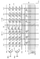
図5は、多層マットのセルアレイにおいて、ワード線とビット線を層間で共有する場合のこれらの配線の引き出し方法の一例を示す。ここでは、8層のセルMC0−MC7の柱を示している。ビット線は層ごとに個別に制御したいので、各層のビット線BL0−BL3は別々に下地制御回路に配線する。一方ワード線は下地回路へのコンタクト領域の面積を削減するために、できる限り共通化してグループを少なくしたい。セルの多重アクセスを生じない最小のグループ数は2であり、これらのグループをevenとoddと命名し、WLe(又はWL(0))とWLo(又はWL(1))で表すと図の接続関係となる。 FIG. 5 shows an example of a method for drawing out these wirings when a word line and a bit line are shared between layers in a multilayer mat cell array. Here, the pillars of the eight-layer cells MC0 to MC7 are shown. Since the bit lines are to be controlled individually for each layer, the bit lines BL0 to BL3 of each layer are wired separately to the base control circuit. On the other hand, in order to reduce the area of the contact region to the underlying circuit, the word lines should be shared as much as possible to reduce the number of groups. The minimum number of groups that do not cause multiple access of cells is 2, and these groups are named even and odd, and are represented by WLe (or WL (0)) and WLo (or WL (1)). It becomes a relationship.
このようなワード線のグループ分けの場合、例えばセルMC3が選択セルSCである場合、クロスフェールのリーク電流は、選択層の上下2層(MC4,5及びMC2,3)の分が選択ワード線WLoに集中する。従って、全ての層でのクロスフェールリークが選択ワード線WLoが属するグループを駆動するドライバに集中してしまうことが予想される。これは、3Dセルアレイの特徴である多層化に限界をもたらす。 In the case of such word line grouping, for example, when the cell MC3 is the selected cell SC, the leakage current of the cross-fail is the selected word line corresponding to the upper and lower layers (MC4, 5 and MC2, 3) of the selected layer. Concentrate on WLo. Therefore, it is expected that cross-fail leaks in all layers are concentrated on the driver that drives the group to which the selected word line WLo belongs. This brings a limit to the multi-layering characteristic of the 3D cell array.
このようなリーク電流の集中の様子を、以下いくつかのグループ分けについて具体的に検討する。 The state of concentration of such leakage current will be specifically examined below for several groupings.
[binaryグループ化の場合のリークの影響]
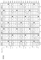
図6は、16層マット構成で、上に説明した2グループ分けの場合(binaryの場合)である。左側に異なるワード線とビット線に属するセルをイメージして16層のマットを二つのメモリセルの柱として示す。下線を付した番号が、下から数えたマット番号である。グループ番号は、バイナリの場合は0と1がワード線ごとに交互に繰り返される。
[Effect of leak in case of binary grouping]
FIG. 6 shows a 16-layer mat structure in the case of the two groups described above (binary case). On the left side, 16-layer mats are shown as two memory cell pillars, imagining cells belonging to different word lines and bit lines. The underlined number is the mat number counted from the bottom. In the case of a binary group number, 0 and 1 are alternately repeated for each word line.
右側の表は、16層マット内でのセルを選択する際のワード線とビット線のレベルと、それらの間のセルを介して流れる電流とその方向とを、マット番号0〜4を選択した場合について示している。表の中の各欄が、マット選択時の交互に重ねられるワード線群とビット線群のレベルを示している。即ち最下層の欄が、マット番号0対応のワード線群WL0の欄、次が同じマット番号0対応のビット線群BL0であり、以下同様に、WL1,BL1,WL2,BL2,…,WL7,BL7,WL8が重ねられる様子を示している。
In the table on the right side, the
そして表の各欄には、マット内で選択されたセルと非選択セルのレベルを並列して示している。即ちワード線は選択/非選択レベル関係を太文字のL/Hで表し、ビット線は選択/非選択レベル関係を小文字のh/lで示している。 In each column of the table, the levels of the cells selected in the mat and the non-selected cells are shown in parallel. That is, the word line indicates the selection / non-selection level relationship by bold L / H, and the bit line indicates the selection / non-selection level relationship by lowercase h / l.
マット0でセルが選択されると、最左端の表に示すように、ビット線群BL0内で選択ビット線がh(=〜Vdd)になり、非選択ビット線はl(=Vs*)となり、またワード線群WL0内で選択ワード線がL(=Vss)、非選択ワード線がH(=Vd*)を保つ。残りのマットのビット線は、全て非選択レベルlである。白丸で示すワード線グループ0の他のマット3,7,11,15対応のワード線群WL2,WL4,WL6,WL8では、選択セルを含むマットにおけると同様に選択/非選択=L/Hが設定される。黒丸で示すグループ1のマットでは、ワード線は非選択状態Hである。
When a cell is selected with
従って、マット0でセルが選択されたとき、実線矢印で示す選択セル電流Icが選択ビット線から選択ワード線に向かって流れる。破線矢印のように、ダイオードの逆耐圧特性またはクロス不良によりワード線からビット線へのリーク電流Ilがあり、バイナリの場合全てのマットでこのリーク電流Ilが流れうる。
Therefore, when a cell is selected with
マット1,2,3,4のセルが選択される場合についても同様に示してある。
The same applies to the case where cells of
これらの表からも分かるように、binary の場合は選択セル以外の全てのセルが逆バイアス状態になるので全てのマットからのリーク電流がワード線グループから流れ出る。マットの数が多い場合(すなわち積層されるメモリセルの層が多い場合)は全てのセルの影響を考慮する必要があり、考慮しなければならない電流量はとても大きくなる。 As can be seen from these tables, in the case of binary, all cells other than the selected cell are in a reverse bias state, so that leakage current from all mats flows out from the word line group. When the number of mats is large (that is, when there are many layers of stacked memory cells), it is necessary to consider the influence of all the cells, and the amount of current that must be taken into consideration becomes very large.
[ternaryグループ化の場合のリークの影響]
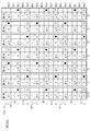
図7は、同様の16マット構成で3グループ分けの場合(ternary の場合)である。即ちワード線群WL0,WL3,WL6をグループ0、ワード線群WL1,WL4,WL7をグループ1、ワード線群WL2,WL5,WL8をグループ2と設定している。
[Effect of leak in case of ternary grouping]
FIG. 7 shows a case of three groups with the same 16 mat configuration (in the case of ternary). That is, the word line groups WL0, WL3, WL6 are set as
表はそれぞれマット0,1,2,3,4,5,6のセルを選択する際のワード線とビット線のレベルと、セルを介して流れる電流の種別と方向を、図6の場合と同様の関係で示している。
The table shows the levels of word lines and bit lines when selecting cells of
マット0のワード線が選択されたとき、白丸で示すように、グループ0の他のマット6,12で、マット0におけると同様に、ワード線群WL3,WL6の選択/非選択=L/Hが設定される。黒丸で示すグループ1のマット2,8,14では、ワード線は非選択状態Hである。
When the word line of the
しるしのつけていないワード線群WL2,WL5,WL8は、マット選択には関係がなくLレベルのままでよいワード線グループ2である。
The word line groups WL2, WL5, and WL8 that are not marked are the
マット0選択のときの選択セル電流Icは、選択ビット線から選択ワード線に向かって流れる。このとき、ビット線群BL0,BL3,BL6にはその上下のワード線から、またビット線群BL2,BL5には上のワード線のみから流れ込む破線のリーク電流Il1は、ダイオードの逆耐圧特性またはクロス不良によるリーク電流である。グループ1のワード線(ワード線群WL1,WL4,WL7)から上のビット線に向かって流れる破線で示すリーク電流Il2は、選択ワード線グループに対して影響がないリーク電流である。グループ2のワード線(ワード線群WL2,WL5,WL8)は、マット選択に関係なく、“L”レベルのまま、即ちセルダイオードが略ゼロバイアスの非活性状態に保持される。
When the
マット1,2,3,4,5,6のセルが選択される場合についても同様に示してある。
The same applies to the case where cells of
これらの表から、ternary の場合は選択セル以外の全てのセルの3分の2が逆耐圧特性になり、逆耐圧リークの影響は3分の2になる。クロス不良の影響は全セルの2分の1について現れ、リーク電流がワード線から流れる出ることが分かる。従ってbinary の場合と比べると、リーク電流の選択ワード線グループへの影響をかなり軽減できる。 From these tables, in the case of ternary, two-thirds of all cells other than the selected cell have reverse breakdown voltage characteristics, and the influence of reverse breakdown voltage leakage is two-thirds. It can be seen that the influence of the cross failure appears for one half of all the cells, and a leak current flows out from the word line. Therefore, compared with the binary case, the influence of the leakage current on the selected word line group can be considerably reduced.
[quadrupleグループ化の場合のリークの影響]
図8は、同様の16マット構成で4グループ分けの場合(quadrupleの場合)である。即ちワード線群WL0,WL4,WL8をグループ0、ワード線群WL1,WL5をグループ1、ワード線群WL2,WL6をグループ2、ワード線群WL3,WL7をグループ3、と設定している。
[Effect of leak in case of quadruple grouping]
FIG. 8 shows a case where four groups are divided in the same 16 mat configuration (in the case of quadruple). That is, the word line groups WL0, WL4, WL8 are set as
表はそれぞれマット0〜8のセルを選択する際のワード線とビット線のレベルと、セルを介して流れる電流の種別と方向を、図6の場合と同様の関係で示している。
The table shows the levels of word lines and bit lines when selecting cells of
マット0のワード線が選択されたとき、白丸で示すように、グループ0の他のマット7,15で、マット0におけると同様に、ワード線群WL4,WL8の選択/非選択=L/Hが設定される。黒丸で示すグループ1のマット2,10では、ワード線は非選択状態Hである。
When the word line of the
しるしのつけていないワード線群WL2,WL3,WL6,WL7は、マット選択には関係がなくLレベルのままでよいワード線グループ2,3である。
The word line groups WL2, WL3, WL6, and WL7 that are not marked are the
マット0選択のときの選択セル電流Icは、選択ビット線から選択ワード線に向かって流れる。このとき、ビット線群BL0,BL4にはその上下のワード線から、またビット線群BL3,BL7に上のワード線のみから流れ込む破線のリーク電流Il1は、ダイオードの逆耐圧特性またはクロス不良によるリーク電流である。ワード線群WL1,WL5から上のビット線に向かって流れる破線で示すリーク電流Il2は、選択ワード線グループに対して影響がないリーク電流である。
When the
マット1〜8のセルが選択される場合についても同様に示してある。
The same applies to the case where cells of
これらの表から、quadruple の場合は選択セル以外の全てのセルの2分の1が逆耐圧特性になり、逆耐圧リークの影響は2分の1になり、クロス不良の影響はリーク電流Il2の部分であり、全セルの8分の3に対して影響する。従って、ternary の場合と比べて更に、リーク電流の選択ワード線グループへの影響を軽減できることになる。 From these tables, in the case of quadruple, one half of all cells other than the selected cell have reverse breakdown voltage characteristics, the influence of reverse breakdown voltage is one half, and the influence of cross failure is the leakage current Il2. It is a part and affects 3/8 of all cells. Therefore, the influence of the leakage current on the selected word line group can be further reduced as compared with the ternary case.
[グループ選択ロジック]
上述のように、ワード線の選択グループを、binary, ternary, quadruple と増やすと、リーク電流の選択ワード線グループへの影響を小さく出来ることが分かった。この場合、ワード線はマット間で共用されるため、グループ間の選択ロジックに工夫がいる。次にこのワード線選択ロジックを説明する。
[Group selection logic]
As described above, it has been found that the influence of the leakage current on the selected word line group can be reduced by increasing the number of selected word line groups to binary, ternary, and quadruple. In this case, since the word line is shared between mats, the selection logic between groups is devised. Next, the word line selection logic will be described.
図9は、16層マットの例でのセルの柱の図に、3種のワード線グループをまとめて示している。 FIG. 9 collectively shows three types of word line groups in the column of cells in the 16-layer mat example.
図10は、図9に示すそれぞれのワード線グループ化の場合について、グループ選択に属するマット番号をグループ毎にまとめて示している。前述のようにワード線は隣接マットで共有されるので、binaryの場合には、どのグループのセルが選択されても、全てのグループ(即ち全てのマット)を活性化する必要がある。この場合マット番号は、4を法とする(0,1,2,3)の合同数としてまとめることができ、これをmod 4の欄に示した。
FIG. 10 collectively shows mat numbers belonging to group selection for each group for each word line grouping shown in FIG. As described above, since word lines are shared by adjacent mats, in the case of binary, it is necessary to activate all groups (that is, all mats) regardless of which group of cells is selected. In this case, the mat numbers can be summarized as a congruent number of (0, 1, 2, 3) modulo 4 and this is shown in the column of
ternaryの場合は、ワード線グループは0,1,2であり、これらのワード線選択に属するマット番号は、mod 6で整理できる。選択されるセルの属するマット番号のmod 6の剰余は二つのワード線グループに属するので、ワード線グループのうちのひとつは活性化する必要がない。
In the case of “ternary”, the word line groups are 0, 1, and 2, and the mat numbers belonging to these word line selections can be arranged by
quadrupleの場合は、ワード線グループは0,1,2,3であり、これらの選択に属するマット番号はmod 8で整理できる。選択されるセルの属するマット番号のmod 8の剰余は二つのワード線グループに属するので、ワード線グループのうちの二つは活性化する必要がない。
In the case of quadruple, the word line groups are 0, 1, 2, 3 and the mat numbers belonging to these selections can be organized by
以上を一般化すると、図10の最下欄に示すように、ワード線グループの分け方を“i-ary”として、ワード線グループをi−k(k=1〜i)、即ち0,1,2,…,i−2,i−1で表すことができ、選択されるセルの属するマット番号がmであれば、活性化するワード線グループ番号は、mのmod 2iの剰余が−2k−2,−2k−1,−2k,−2k+1に相当するkから計算したi−kとなる。
When the above is generalized, as shown in the bottom column of FIG. 10, the word line group is divided into “i-ary” and the word line group is set to ik (k = 1 to i), that is, 0, 1 , 2,..., I-2, i-1 and if the mat number to which the selected cell belongs is m, the word line group number to be activated is the remainder of
[具体的なリークの影響]
以上、ワード線グループの分割とマット選択の規則についてまとめたが、これらを実際に3Dセルアレイに適用する際の具体的な方法について説明する。まずワード線を3以上のグループに分けた場合について、セルアレイのリークの影響を具体的に見てみる。
[Specific leak effects]
The rule of word line group division and mat selection has been summarized above, and a specific method for actually applying these to a 3D cell array will be described. First, the effect of cell array leakage will be specifically examined when the word lines are divided into three or more groups.
図11は、図4と同様にセルアレイMA0〜MA6の7層分のマット構成について、ちょうど真中のマットのセルSCがアクセスされた場合に各種電流の流れる様子を、ワード線グループ分けが3以上の場合(具体的にはternaryの場合)について示したものである。選択セルSCは、太線で示すワード線WL32と同じく太線で示すビット線BL22によって選択される。ここでは、セット状態への書き込みの場合(セット動作)を示しており、選択ビット線BL22にはほぼVddが印加され、選択ワード線WL22はVssにドライブされる。 FIG. 11 shows a state in which various currents flow when the cell SC of the middle mat is accessed in the mat structure for seven layers of the cell arrays MA0 to MA6 as in FIG. The case (specifically, the case of tertiary) is shown. The selected cell SC is selected by the bit line BL22 indicated by the bold line as well as the word line WL32 indicated by the bold line. Here, a case of writing to a set state (set operation) is shown, and Vdd is substantially applied to the selected bit line BL22, and the selected word line WL22 is driven to Vss.
選択セルSCの属するマットのワード線グループ2の中の選択ワード線WL32以外の非選択ワード線(WL31,WL33)は、Vd*(VddよりダイオードのVf程度低い電位)に設定する。ワード線グループ0のワード線(WL11−WL13,WL41−WL43)は全てVs*(VssよりダイオードのVf程度高い電位)、ワード線グループ1のワード線WL21−WL23は全て、Vd*とする。
The unselected word lines (WL31, WL33) other than the selected word line WL32 in the mat
非選択ビット線は全てフローティングのVs*となる。 All the non-selected bit lines become floating Vs * .
不良セルは、図4の場合と同様、セルアレイMA1内のセルDC1、セルアレイMA2内のセルDC2、セルアレイMA3内のセルDC3、セルアレイMA4内のセルDC4、セルアレイMA5内のセルDC5、セルアレイMA6内のセルDC6である。これらのうち、選択セルへ影響の大きな不良セルは、DC2,DC3,DC4である。 As in the case of FIG. 4, the defective cells are the cells DC1 in the cell array MA1, the cell DC2 in the cell array MA2, the cell DC3 in the cell array MA3, the cell DC4 in the cell array MA4, the cell DC5 in the cell array MA5, and the cell array MA6. This is the cell DC6. Among these, DC2, DC3, and DC4 are defective cells having a great influence on the selected cell.
不良セルの属するビット線(不良ビット線)は常にフローティングであり、その他の非選択ビット線はVs*に設定されアクセスの短い期間だけフローティングに設定されるで、アクセス期間中は不良ビット線のレベルは不良セル経由のワード線レベルVd*からのリークによってVd*−αとなる。 The bit line to which the defective cell belongs (defective bit line) is always floating, and the other non-selected bit lines are set to Vs * and set to floating only for a short access period. Becomes Vd * −α due to leakage from the word line level Vd * via the defective cell.
このアクセス状態でのリーク電流は図のような状況となる。Vssに設定された選択ワード線WL32には選択セルSCの属するマットとその上下のマットの不良セルのリーク電流が本来のセル電流Icに加えて流れ込む。即ち不良セルDC2,DC3,DC4のリーク電流Idが、隣接ビット線を通り、選択ワード線WL32に流れ込んで、セル電流Icに加算される。 The leakage current in this access state is as shown in the figure. In addition to the original cell current Ic, the leakage current of the defective cell of the mat to which the selected cell SC belongs and the mat above and below it flows into the selected word line WL32 set to Vss. That is, the leakage current Id of the defective cells DC2, DC3, DC4 flows through the adjacent bit line and flows into the selected word line WL32, and is added to the cell current Ic.
それ以外のマットの例えば不良セルDC1のリーク電流Ipは、非選択ワード線としてVs*に設定されたワード線WL11,WL12,WL13に分散して流れ込む。また選択ビット線BL22は、セット状態への書込みではVdd程度の電位に設定されるので、選択ワード線グループの非選択ワード線のレベルVd*よりダイオードのVf程度電位が高く、これに接続されるセルにわずかながらオン電流が流れる可能性がある。このオン電流リークIqは個々の非選択ワード線に分散して流れ込む。 For example, the leakage current Ip of the defective cell DC1 of other mats flows in a distributed manner to the word lines WL11, WL12, WL13 set to Vs * as the unselected word lines. Since the selected bit line BL22 is set to a potential of about Vdd in writing to the set state, the potential is about Vf of the diode higher than the level Vd * of the unselected word line of the selected word line group, and is connected to this. A small amount of on-current may flow through the cell. This on-current leakage Iq flows in a distributed manner into the individual unselected word lines.
但し、上述の選択ビット線からのリーク電流Iqは、セット状態への書き込みの場合だけであり、このときはセルが高抵抗状態でこれら電流の総和もリセット状態への書き込みの場合に比べてオーダーが十分小さいから、選択ビット線のレベルを変えるほどではなく、セット状態への書き込み動作に対す影響は無視できる。 However, the leakage current Iq from the selected bit line described above is only in the case of writing to the set state, and in this case, the sum of these currents is higher than that in the case of writing to the reset state when the cell is in the high resistance state. Is sufficiently small, the influence on the write operation to the set state is negligible, not enough to change the level of the selected bit line.
以上から、選択ワード線のVssへのドライブはそのドライブ電流に選択マットとその上下の1層内の不良セルのリークが加算されるので、十分に低インピーダンスにして電流シンクとしての役割を十分働かせる必要がある。非選択ワード線の設定電位Vs*やVd*へのドライブについては、弱い順方向電流が分散して流れ込むのでインピーダンスをむしろ高くしてこれらの電流を抑えることが良い。 From the above, when the selected word line is driven to Vss, the leakage of the selected mat and the defective cells in the upper and lower layers is added to the drive current. There is a need. For driving the unselected word lines to the set potentials Vs * and Vd * , weak forward currents flow in a distributed manner, so it is preferable to suppress these currents by rather increasing the impedance.
[WL及びBL選択回路]
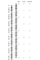
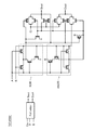
図12は、ワード線及びビット線選択回路部の詳細構成を示している。3Dセルアレイは、センスアンプ(SA)106を共有するビット線群の範囲をひとつのセルアレイユニット(以下、スタンバイユニットという)100として、それらのビット線群の一つがビット線選択回路103により選択されて、ローカルバスLB_mに接続される。ビット線選択回路103としてここでは簡略に選択トランジスタであるNMOSトランジスタQN2のみ示している。
[WL and BL selection circuit]
FIG. 12 shows a detailed configuration of the word line and bit line selection circuit unit. In the 3D cell array, a range of bit lines sharing the sense amplifier (SA) 106 is defined as one cell array unit (hereinafter referred to as a standby unit) 100, and one of those bit line groups is selected by the bit
ワード線ドライバ101は、選択ワード線をVssに設定するためのNMOSトランジスタQN1と、非選択ワード線にVd*を与えるためのPMOSトランジスタQP1からなるCMOSドライバである。これらは、出力インピーダンスを出来る限り小さくして、クロスフェールに対しても、選択,非選択共に十分なレベルが保持できるようにする。
The
状態遷移安定化回路104は、ローカルバスLB_mを介して選択ビット線に接続されるNMOSトランジスタMN及びPMOSトランジスタMPの部分である。
The state
ビット線リセット回路105は、非選択ビット線をVs*に設定するための回路であり、NMOSトランジスタQN4を用いて構成される。このNMOSトランジスタQN4のソース側には、不良セル検出用NMOSトランジスタMが挿入されている。
The bit
ワード線及びビット線の電位設定のためには、接地レベルVssよりダイオードの順方向降下電圧Vf分高い電位Vs*を生成し、セット電圧より高い電源電位VddよりVfだけ低い電位Vd*を生成するようにしている。 In order to set the potential of the word line and the bit line, a potential Vs * that is higher than the ground level Vss by the diode forward drop voltage Vf is generated, and a potential Vd * that is lower than the power supply potential Vdd higher than the set voltage by Vf is generated. I am doing so.
ワード線ドライバ101は、制御信号wlsel_x(x=k,k+1,…)により制御されて、選択されたひとつのワード線(選択ワード線)をVssに、残りの非選択ワード線をVd*に設定する。ワード線選択信号wlsel_xはセルデータを保持しておくホールド状態では“H”、セルのアクセスがいつでも可能なスタンバイ状態以降では、非選択で“L”、選択で“H”となる信号である。
The
ビット線デコードに関しては、スタンバイユニット100の共通のデータバスであるローカルバスLB_mに各々のビット線が選択的に接続されるが、この選択を行なうのがビット線選択信号blsel_yである。この信号はビット線に十分なレベルを伝達するためにNMOSトランジスタQN2を用いるときは、“H”レベルとしてVdd+Vtより高いレベルをもつ信号である。即ちビット線選択信号blsel_y(y=i,i+1,…)は、非選択時はすべてVddレベルの“H”であり、選択されたスタンバイユニット属するビット線対応の信号は、Vdd+Vtより高いレベルの“H”になり、非選択ビット線対応の信号はVssレベルの“L”となる。
Regarding bit line decoding, each bit line is selectively connected to the local bus LB_m, which is a common data bus of the
不良セルを検出して、不良セルにつながるビット線(即ち不良ビット線)をフローティングにする手法を次に説明する。 A method for detecting a defective cell and floating a bit line (that is, a defective bit line) connected to the defective cell will be described next.
スタンバイ時には、全てのビット線選択信号blsel_y(y=i,i+1,…)が“H”であり、ローカルバスLB_mは、フラグ信号flag_mが“H”に設定されてセンスアンプ106からも切り離されるので、ローカルバスのレベルが全てのビット線に設定される。具体的に言えば、ローカルバスLB_mのレベルは、ローカルバス選択信号/lcbsel_mが“H”で、信号/flag_mも“H”に設定されてNMOSトランジスタQN4及びMが共にオンであるので、Vs*である。
At the time of standby, all the bit line selection signals blsel_y (y = i, i + 1,...) Are “H”, and the local bus LB_m is disconnected from the
スタンバイユニット100にリークの大きな不良セルがある場合、ワード線WLのVd*レベルから電流がビット線BLを介してローカルバスLB_mに流れてくる。この電流はVs*に流れ込むが、ゲートレベルが“H”であるセンス用NMOSトランジスタMを通る際に、そのドレインノード(ビット線電流モニターノード)IM_mのレベルを引き上げる。このモニターノードIM_mのレベル変化を検出して不良セルの有無の判定を行う。
When there is a defective cell having a large leak in the
フリップフロップ回路107は、上述した不良セルの有無判定回路である。この判定回路107は、CMOSインバータ108,109の入出力をクロスカップルして構成されている。CMOSインバータ109の入力ノードが、NMOSトランジスタQN10を介してモニターノードIM_mに接続され、その出力ノードがフラグ信号/flag_mの出力ノードとなる。CMOSインバータ109の入力ノードには、リセット用NMOSトランジスタQN11が接続されている。
The flip-
この判定回路107は、ホールド状態ではHS=“H”により、/flag_m=“H”なる初期状態に設定される。スタンバイ状態になると信号“stdby”が“H”になり、HSが“L”になるので、モニターノードIM_mのレベルを受けて状態を変化することが出来る。ある定められた不良があれば、IM_mのレベル上昇によりフリップフロップの状態が反転し、/flag_mが“L”になる。
The
ここで判定回路107のフリップフロップ構成は、CMOSインバータ108の寸法をCMOSインバータ109のそれより小さくしして、モニターノードIM_mから電流を多く引き込まないようにする。また、入力側のインバータ109のしきい値を最適設定することにより、リークの許容値を設定する。
Here, in the flip-flop configuration of the
信号/flag_mが“L”になると、flag_mの“H”でローカルバスが選択されて、lcbsel_mが“H”になっても“H”のままであり、センスアンプ系が切り離された状態を維持する。またこのときトランジスタMもオフとなるので、ローカルバスLB_mはフローティングになり、ビット線は選択されてもフローティング状態となる。 When the signal / flag_m becomes “L”, the local bus is selected by “H” of the flag_m, and even if lcbsel_m becomes “H”, it remains “H” and the sense amplifier system is kept disconnected. To do. At this time, since the transistor M is also turned off, the local bus LB_m is in a floating state, and even if the bit line is selected, it is in a floating state.
不良がないときには信号/flag_mが“H”であるので信号stdbyが“L”になりローカルバス選択信号lcbsel_mが“H”になると、flag_mが“L”となり、ローカルバスLB_mとセンスアンプ系がつながる。この際ローカルバスは、信号/lcbsel_mが“L”になるので、Vs*とは切り離される。 When there is no defect, the signal / flag_m is “H”, so when the signal stdby becomes “L” and the local bus selection signal lcbsel_m becomes “H”, the flag_m becomes “L”, and the local bus LB_m and the sense amplifier system are connected. . At this time, since the signal / lcbsel_m becomes “L”, the local bus is disconnected from Vs * .
その後アクセスサイクルに入り、選択ビット線の選択信号blsel_yのみがVdd+Vt以上の“H”レベルになり、他の非選択ビット線はローカルバスLB_mから切り離されてフローティングとなる。 Thereafter, an access cycle is entered, and only the selection signal blsel_y of the selected bit line becomes “H” level equal to or higher than Vdd + Vt, and the other unselected bit lines are disconnected from the local bus LB_m and become floating.
[メモリチップの構成と活性化方式]
図13は、メモリチップの構成と活性化の選択のひとつの方式を説明するための図である。ここでは、一つのセルアレイブロックが32マットで、1マットが1k本のワード線を有し、一つのメインワード線を選択することにより複数の部分ワード線ドライバに選択信号が送られて、複数のワード線が選択される、ダブルワード線スキーム方式の場合を想定している。
[Memory chip configuration and activation method]
FIG. 13 is a diagram for explaining one method of selecting a memory chip configuration and activation. Here, one cell array block has 32 mats, one mat has 1k word lines, and by selecting one main word line, a selection signal is sent to a plurality of partial word line drivers, The case of the double word line scheme method in which the word line is selected is assumed.
8個のセルアレイブロックMB0−7が、×8I/O構成で同時選択される一つのアレイグループを構成するものとして、ここでは二つのアレイグループAG0,AG1が配置された例を示している。 Here, an example is shown in which two array groups AG0 and AG1 are arranged, assuming that eight cell array blocks MB0-7 constitute one array group simultaneously selected in the × 8 I / O configuration.
まずアドレスビットの割付であるが、A0〜A6をメインワード線(MWL)選択に、A7〜A9を部分ロウデコーダ(PRDC)の選択に適用する。すなわちA0からA9を1k本のワード線選択に関わるビットとする。 First, regarding address bit allocation, A0 to A6 are applied to the main word line (MWL) selection, and A7 to A9 are applied to the selection of the partial row decoder (PRDC). That is, A0 to A9 are bits related to 1k word line selection.
セルアレイの層である32マットの選択にはA10〜A14を用いる。A15はアレイグループAG0,1の選択に関わる部分とする。 A10 to A14 are used to select 32 mats which are the cell array layers. A15 is a part related to selection of the array groups AG0, AG1.
メモリチップはセルアレイブロック16個により構成され、1バイト(=8ビット)のデータを同時に扱う×8I/O構成のメモリとし、アクセスはセルアレイあたり1セルのみにアクセスできるとする。従って×8においては、いずれかのグループAG0,AG1で同時に8セルアレイブロックMB0〜MB7にアクセスすることになる。 The memory chip is composed of 16 cell array blocks. The memory chip has a × 8 I / O configuration that simultaneously handles 1 byte (= 8 bits) of data, and only one cell can be accessed per cell array. Therefore, in x8, one of the groups AG0 and AG1 accesses the 8 cell array blocks MB0 to MB7 at the same time.
4セルアレイブロックにまたがるメインワード線MWLの一端側にメインワード線デコーダ(MWLdec)131が配置される。また同時選択アレイグループのセルアレイブロックMB0,MB4の間、同様にMB1,MB5の間、MB2,MB6の間、MB3,MB7の間にそれぞれ、部分ロウデコーダPRDCとこれに信号を転送する転送ゲート回路132が配置される。 A main word line decoder (MWLdec) 131 is arranged on one end side of the main word line MWL across four cell array blocks. Also, a partial row decoder PRDC and a transfer gate circuit for transferring signals to the cell array blocks MB0 and MB4 of the simultaneously selected array group, similarly between MB1 and MB5, between MB2 and MB6, and between MB3 and MB7, respectively. 132 is arranged.
転送ゲート回路132に供給される信号は、PRDCを選択的に駆動する信号PRDCi(=PRDC0〜PRDC7)と、マットのワード線グループを選択されたマットに従って活性化するための選択信号WGi(=WG0〜WG2)である。これらはそれぞれアドレスビットA7〜A9とA10〜A14からデコードされる。
The signal supplied to the
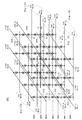
図14は、これらの信号WGi,PRDCiを更にデコードしてワード線選択を行う部分、即ち図13の転送ゲート回路132の部分と、ワード線ドライバ141及び部分ロウデコーダ142の構成を示す。これはセルアレイブロック間の回路であるので出来るだけ簡単な構成で必要最小限の機能を満たすように構成することが重要となる。ここに示す回路はternaryのワード線を選択する場合を想定して構成したものである。
FIG. 14 shows a configuration for further decoding these signals WGi and PRDCi to select a word line, that is, a portion of the
y方向に走る信号PRDCi,WGi,/WGiが全てのセルアレイで使用される共通の信号であり、これらの信号を更にデコードして選択セルアレイで固有のワード線選択信号とする各デコーダ回路が示されている。図中、WCは、3Dセルアレイブロックのワード線グループ毎に共通の垂直配線が基板回路部に落ちてくるワード線コンタクトを示しており、ここに出力を与えるドライバ群がワード線ドライバ141を構成している。
Signals PRDCi, WGi, / WGi running in the y direction are common signals used in all cell arrays, and each decoder circuit is further decoded to generate a unique word line selection signal in the selected cell array. ing. In the figure, WC indicates a word line contact in which a common vertical wiring falls to the substrate circuit portion for each word line group of the 3D cell array block, and a driver group that provides an output forms a
今の場合、ternaryであるので、セルアレイブロック毎にワード線グループは、W.G.0〜W.G.2の3系列ある。図14では、左右に隣接する二つのセルアレイブロック例えば、MB0とMB1に共通のデコーダ回路部を示しているので、それぞれのセルアレイブロックに対応した3つずつのワード線グループのワード線コンタクトWCを持つ。 In this case, since it is ternary, the word line group for each cell array block is W.W. G. 0-W. G. There are two three series. FIG. 14 shows a decoder circuit unit common to two cell array blocks adjacent to the left and right, for example, MB0 and MB1, and therefore has word line contacts WC of three word line groups corresponding to each cell array block. .
信号のインバータとして働く回路は2種類ありこれをシンボル化している。即ち、NMOSトランジスタのソースがVssに接続され、PMOSトランジスタのソースに信号が入力されるインバータINV1を、インバータ記号の上側に下向き矢印を加えて示し、NMOSトランジスタ、PMOSトランジスタともソースに信号入力されるインバータINV2を、インバータ記号の上下に内向きの矢印を付して示した。いずれにおいても、NMOSトランジスタのゲート幅wは大きくしてオンインピーダンスを減らしている。 There are two types of circuits that function as signal inverters, which are symbolized. That is, the inverter INV1 in which the source of the NMOS transistor is connected to Vss and a signal is input to the source of the PMOS transistor is indicated by adding a downward arrow above the inverter symbol, and both the NMOS transistor and the PMOS transistor are input to the source. The inverter INV2 is shown with inward arrows above and below the inverter symbol. In any case, the gate width w of the NMOS transistor is increased to reduce the on-impedance.
転送ゲート回路132において、信号WGi,/WGiがワード線グループ選択信号としてワード線ドライバ141の各ドライバに送られる、また信号PRDC0〜3がセルアレイブロックMB0,MB1間の部分ロウデコーダ142に送られる。
In
点線で囲ったワード線ドライバ141はメインワード線信号/MWLの数だけ繰り返される。なお、セルアレイブロックのワード線WLは、図1で説明したように、各セルアレイで左右の辺から交互に配線されるので、図の部分デコーダ回路142を挟む左右のセルアレイブロックはレイアウト的には一般的に左右反転した形になる。この図の隣の部分ロウデコーダ回路(セルアレイブロックMB2,MB3の間の部分ロウデコード回路)には、信号PRDC0〜3の代わりに信号PRDC4〜7が接続されていて、メインワード線信号/MWLあたりひとつのセルアレイブロックで8本のワード線WLを選択駆動する。
以下に信号(線)の簡単な説明をまとめる。 A brief description of signals (lines) is summarized below.
/MWLx:選択される全ての(8個の)セルアレイブロックに共通のメインワード線(信号)で、メインワード線デコーダ(MWLdec)131で発生されて各セルアレイブロック間に配置される部分ロウデコーダ142を選択する。
/ MWLx: Main word line (signal) common to all (eight) cell array blocks to be selected.
Vd*:電源電位Vddよりダイオードの順方向電圧降下Vf程度低いレベルの電源線。 Vd * : a power supply line at a level lower than the power supply potential Vdd by about a forward voltage drop Vf of the diode.
Vs*:接地電位VssよりダイオードのVf程度高いレベルの電源線。 Vs * : A power supply line having a level higher than the ground potential Vss by about Vf of the diode.
/WGc0〜2:選択されたセルのワード線グループとそれに随伴して選択されるワード線グループを合わせて選択する信号WGc0〜2の反転信号。 / WGc0-2: Inversion signals of signals WGc0-2 that select the word line group of the selected cell and the word line group selected accordingly.
WG0〜2:選択されたセルのワード線グループの選択信号。 WG0-2: Selection signals for the word line group of the selected cell.
PRDC0〜3:セルアレイブロックの一方のワード線端部側の部分ワード線ドライバ回路に選択的に供給される駆動信号。 PRDC0 to PRDC3: Drive signals selectively supplied to the partial word line driver circuit on one word line end side of the cell array block.
PRDC4〜7:セルアレイブロックの他方のワード線端部側の部分ワード線ドライバ回路に選択的に供給される駆動信号。 PRDC4 to 7: Drive signals selectively supplied to the partial word line driver circuit on the other word line end side of the cell array block.
図15は、図14のデコード回路に従ったワード線のレベルの設定値をまとめたものである。表記について、電源信号へのワード線接続のインピーダンス状態をH,H’及びLで表す。 FIG. 15 summarizes the set values of the word line levels according to the decoding circuit of FIG. Regarding the notation, the impedance state of the word line connection to the power supply signal is represented by H, H ′ and L.
Hは、Vd*がNMOSトランジスタを介して、またはVs*がPMOSトランジスタを介してワード線に供給される部分を含むことを示し、電源へといたるパスがハイインピーダンスであることを表す。H’は、Vd*がPMOSトランジスタを介して供給されるが、トランジスタのゲートレベルがVth分だけロスがあり、トランジスタのコンダクタンスが少し小さく、その分だけハイインピーダンスであることを表す。Lは、電源信号が、トランジスタにおけるロスがなく本来のインピーダンスで供給される場合である。 H indicates that Vd * includes a portion supplied to the word line via the NMOS transistor or Vs * via the PMOS transistor, and indicates that the path to the power supply is high impedance. H ′ represents that Vd * is supplied via the PMOS transistor, but the gate level of the transistor has a loss by Vth, the conductance of the transistor is slightly small, and the impedance is high by that amount. L is a case where the power signal is supplied with the original impedance without any loss in the transistor.
デコーダの選択信号の状態によってワード線のインピーダンス状態とレベルがどうなるかを表に従って見てみる。先ず、表の各欄の意味を説明すると、欄WG/WGcは、WGcが選択と非選択に別れ、選択の場合は、ワード線グループがセルアクセスとして選択された場合(WG=“H”)と、そのペアして選択された場合(WG=“L”)に分かれる。 Let's see how the impedance state and level of the word line changes according to the state of the selection signal of the decoder according to the table. First, the meaning of each column of the table will be described. In the column WG / WGc, WGc is divided into selected and unselected, and in the case of selection, the word line group is selected as cell access (WG = “H”). And when the pair is selected (WG = “L”).
そのいずれの場合も、メインワード線選択信号MWLが選択か非選択かの場合に分かれる。MWLが選択の場合は、部分ワード線ドラバを選択するので、PRDCが選択と非選択に分かれ、個別のワード線レベルが設定される。 In either case, the main word line selection signal MWL is selected or not selected. When MWL is selected, a partial word line driver is selected, so PRDC is divided into selected and unselected, and individual word line levels are set.
個々のワード線の状態を簡単に見てみると、次の通りである。ワード線インピーダンス−レベルの欄の一番上から順に説明する。 A brief look at the status of individual word lines is as follows. Description will be made in order from the top of the column of word line impedance-level.
・1は選択されたワード線でインピーダンスがLでVssに接続される。 1 is the selected word line, the impedance is L and it is connected to Vss.
・2は選択されたワード線と同じ部分ワード線ドライバに属してPRDC信号によって選択されないワード線であり、PMOSトランジスタのVthロスを介してPMOSトランジスタのゲートレベルを作るので、インピーダンスがH’でVd*に接続される。 2 is a word line that belongs to the same partial word line driver as the selected word line and is not selected by the PRDC signal, and creates the gate level of the PMOS transistor through the Vth loss of the PMOS transistor, so that the impedance is H ′ and Vd Connected to * .
・3は1、2と同じワード線グループに属しているが、MWLで選択されない部分ワード線ドライバに属しているワード線で、PMOSトランジスタのゲートはしっかりVssになるので、インピーダンスがLでVd*に接続される。 3 is a word line belonging to the same word line group as 1 and 2 but belonging to a partial word line driver not selected by MWL. Since the gate of the PMOS transistor is firmly Vss, the impedance is L and Vd * Connected to.
・4は選択ワード線グループの対をなすワード線グループとして選択されるもので、選択セルと同じMWL信号で選択される部分ワード線ドライバに属するワード線であり、PRDC信号によって選択されるワード線であって、Vd*がNMOSトランジスタ側からワード線に接続されるので、インピーダンスがHとなる。 4 is selected as a word line group that forms a pair of selected word line groups, and is a word line belonging to the partial word line driver selected by the same MWL signal as the selected cell, and is selected by the PRDC signal Since Vd * is connected to the word line from the NMOS transistor side, the impedance becomes H.
・5は選択ワード線グループの対をなすワード線グループとして選択されるもので、選択セルと同じMWL信号で選択される部分ワード線ドライバに属するワード線であり、PRDC信号によって選択されないワード線であって、PMOSトランジスタのVthロスを介してPMOSトランジスタのゲートレベルを作るので、インピーダンスがH’でVd*に接続される。 5 is selected as a word line group forming a pair of selected word line groups, and is a word line belonging to a partial word line driver selected by the same MWL signal as the selected cell, and is a word line not selected by the PRDC signal. Since the gate level of the PMOS transistor is created via the Vth loss of the PMOS transistor, the impedance is H ′ and the impedance is connected to Vd * .
・6は4、5と同じワード線グループに属しているが、MWLで選択されない部分ワード線ドライバに属しているワード線で、PMOSトランジスタのゲートはしっかりVssになるので、インピーダンスがLでVd*に接続される。 6 is a word line belonging to the same word line group as 4 and 5 but belonging to a partial word line driver not selected by MWL. Since the gate of the PMOS transistor is firmly Vss, the impedance is L and Vd * Connected to.
・7は非選択のワード線グループに属しているがMWLで選択された部分ワード線ドライバからPRDC信号で選択されるワード線で、 Vd*がNMOSトランジスタ側からワード線に接続されるので、インピーダンスがHとなる。 7 is a word line that belongs to an unselected word line group but is selected by a PRDC signal from the partial word line driver selected by MWL. Since Vd * is connected to the word line from the NMOS transistor side, impedance is Becomes H.
・8は非選択のワード線グループに属しているがMWLで選択された部分ワード線ドライバからPRDC信号で非選択となるワード線で、 PMOSトランジスタ のVthロスを介してPMOSトランジスタのゲートレベルを作るので、インピーダンスがH’であり、Vs*がPMOSトランジスタ側からワード線に接続されるので、インピーダンスはHでもある。 8 is a word line that belongs to a non-selected word line group but is not selected by the PRDC signal from the partial word line driver selected by MWL, and creates the gate level of the PMOS transistor via the Vth loss of the PMOS transistor Therefore, since the impedance is H ′ and Vs * is connected to the word line from the PMOS transistor side, the impedance is also H.
・9は7、8と同じワード線グループに属しているがMWLで選択されない部分ワード線ドライバに属しているワード線で、PMOSトランジスタのゲートはしっかりVssになるが、Vs*がPMOSトランジスタ側からワード線に接続されるのでインピーダンスはHである。 9 is a word line belonging to the same word line group as 7 and 8 but is not selected by MWL, and belongs to a partial word line driver. The gate of the PMOS transistor is firmly Vss, but Vs * is from the PMOS transistor side. The impedance is H because it is connected to the word line.
選択WGc内のワード線はインピーダンスの違いはあるものの非選択セルのワード線はVd*、 選択セルのワード線はインピーダンスLのVssとなり、非選択WG内のワード線は選択セルのワード線に対応するものを除いてインピーダンスHのVs*、選択セル対応ワード線もインピーダンスHのVd*になり、クロスフェールへの影響ほとんどない。 Although the word lines in the selected WGc have different impedances, the word lines of the non-selected cells are Vd * , the word lines of the selected cells are Vss of impedance L, and the word lines in the non-selected WG correspond to the word lines of the selected cells. Except for the above, Vs * of impedance H and the word line corresponding to the selected cell are also Vd * of impedance H, and there is almost no influence on cross failure.
なお、7は本来Vs*へと接続されるのが望ましいが、回路の簡単化からVd*への接続となっている。 Note that 7 is originally preferably connected to Vs * , but is connected to Vd * because of the simplification of the circuit.
この様なワード線のレベル設定でのリーク電流の流れる様子を次に具体的に見ると、図7に対して、図16のようになる。 The state of leakage current flowing with such a word line level setting will be specifically shown in FIG. 16 as opposed to FIG.
ワード線グループは、図7の場合と同様、ternaryであるから、16マットに対して、グループ番号0,1,2で示す3グループに分けられる。図7と対応させて、各マットのワード線選択/非選択状態、ビット線選択/非選択状態、リーク電流の状態を示している。
Since the word line groups are tertiary as in the case of FIG. 7, they are divided into three groups indicated by
マット0でセルが選択されると、最左端の表に示すように、ワード線群WL0の中で選択ワード線がL、非選択ワード線がHとなり、ビット線群BL0の中で選択ビット線がh、非選択ビット線がlとなり、マット0の選択セルにセル電流Icが流れる。
When a cell is selected with
同時に、白丸で示した選択ワード線グループ0と同じグループ0のワード線群WL3,WL6内で選択マットと同様に選択/非選択が設定される。黒丸で示したワード線群WL1,WL4,WL7は、アクセスされたマットに関係したその他のワード線群であり、Hに設定される。何もしるしのないワード線群はマット選択には全く関係がなく、Lレベルのままでよい。
At the same time, selection / non-selection is set similarly to the selection mat in the word line groups WL3 and WL6 of the
図7と同様に、ダイオードの逆耐圧特性またはクロス不良によるリーク電流Il1が流れ、またワード線群WL1,WL4,WL7からそれらの上方のビット線に選択ワード線グループには影響がないリーク電流Il2が流れる。 As in FIG. 7, a leakage current Il1 flows due to the reverse breakdown voltage characteristics or cross failure of the diode, and the selected word line group is not affected from the word line groups WL1, WL4, WL7 to the bit lines above them. Flows.
図7で説明したリーク電流に加えて、選択ワード線と同じ部分ワード線ドライブを受けるワード線群WL2,WL5,WL8において、ワード線のH/Lが設定され、これらから隣接するlレベルのビット線に対して、リーク電流Il3が流れる。従って選択ワード線グループに流れ込む電流は増えるが、非選択ワード線グループ中で図15の“7”の状態になるのは選択ワード線に対応する各マットで1本ずつであるので、実質的なリーク電流の増加はない。 In addition to the leakage current described with reference to FIG. 7, in the word line groups WL2, WL5, WL8 that receive the same partial word line drive as the selected word line, the H / L of the word line is set and the adjacent l-level bit A leakage current Il3 flows through the line. Therefore, the current flowing into the selected word line group increases, but the state of “7” in FIG. 15 in the unselected word line group is one for each mat corresponding to the selected word line. There is no increase in leakage current.
他のマットが選択された場合も同様である。 The same applies when another mat is selected.
以上のリーク電流の状態を、実際に3Dアレイの状況として見たのが、図17であり、これは先の図11に対応する。先の図11と異なる点は、太線で示す選択ワード線WL32に対応する他のマットの非選択ワード線WL12,WL22,WL42が全て、H−Vd*となる点である。図では3系統のワード線群が示されているが、各マット3本ずつ示されたワード線の奥から2本が、メインワード線信号MWLによって同時選択され、手前の1本のワード線がMWLで非選択となったことを示している。 FIG. 17 shows the state of the above leakage current as the state of the 3D array, which corresponds to FIG. The difference from the previous FIG. 11 is that the unselected word lines WL12, WL22, WL42 of other mats corresponding to the selected word line WL32 indicated by the bold line are all H-Vd * . Although three word line groups are shown in the figure, two word lines from the back of the three word lines indicated by each mat are simultaneously selected by the main word line signal MWL, and one word line in front is selected. It shows that it was not selected by MWL.
図ではこれらのワード線に属する不良セルを想定していないのでリーク電流の流れの様子は先の図11の場合と変わらない。逆バイアスとなるセルも新たにワード線グループ0で加わった1本のワード線に属する分である。
In the figure, since the defective cells belonging to these word lines are not assumed, the flow of leakage current is the same as in the case of FIG. The reverse bias cell also belongs to one word line newly added in the
以上、ワード線を3つ以上のグループに分けると、ワード線とビット線をそれぞれ層間で共有化した場合のクロスフェールなどのリーク電流を大幅に削減できることが分かった。次に、図10で示したようなマット選択とワード線グループの選択の関連付けを具体的に回路システムで実現する方法を説明する。 As described above, when the word lines are divided into three or more groups, it has been found that leakage current such as cross-fail when the word line and the bit line are shared between layers can be significantly reduced. Next, a method for realizing the association between mat selection and word line group selection as shown in FIG. 10 in a circuit system will be described.
選択セルの属するマット番号から決まる選択ワード線グループ番号をWG、ペアとして同時に選択される相補的な選択ワード線グループ番号をWGcとする。ワード線グループ数をiとしてWGc=i−k(k=i,i−1,i−2,…,2,1)とする。また、選択セルが属するマットの番号をmとする。mが与えられた時に選ぶワード線グループ番号は、図10で確立していて、2WGc≡−2k≡m−1,m,m+1,m+2(mod 2i)として、kを計算することにより得られる。
The selected word line group number determined from the mat number to which the selected cell belongs is WG, and the complementary selected word line group number selected simultaneously as a pair is WGc. It is assumed that the number of word line groups is i and WGc = i−k (k = i, i−1, i−2,..., 2, 1). Also, let m be the number of the mat to which the selected cell belongs. The word line group number selected when m is given is established in FIG. 10, and is obtained by calculating k as 2WGc≡−2k≡m−1, m, m + 1, m + 2 (
図18はそのようなワード線グループ番号を計算するためのブロック概念を示している。これは、ワード線グループ選択回路でもある。マット番号mが決まるとこれからまず、m−1,m,m+1,m+2を求める。これらの結果を、2iを法としての合同数である既約剰余を求める回路ブロック,residue (mod 2i),に入力して剰余を求める。次に各剰余をワード線グループ番号WGcに対応するデコーダ回路、すなわち2進数で表された剰余の各ビットのANDから2WGcの2進数表現に一致するものを検索し、どれかが一致すれば選択信号としてWGcを立てる。またmの剰余から一致検索を行なった結果を選択信号WGとして、これが選択ワード線グループ番号となる。この一致検索の回路は、WGcが0からi−1のi個必要である。
FIG. 18 shows a block concept for calculating such a word line group number. This is also a word line group selection circuit. When the mat number m is determined, m-1, m, m + 1, m + 2 are first obtained. These results are input to a residue (
[ワード線選択信号発生回路−ternaryの場合]
ternaryの場合(i=3)について具体的なワード線選択信号発生回路を検討する。
[In the case of word line selection signal generation circuit-ternary]
A specific word line selection signal generation circuit will be examined for the ternary case (i = 3).
図19に示すように、マットの総数を32としマット番号がA10〜A14の5ビットで2進表示されるものとする。各アドレスビットとマット番号mの関係は図19の上側の表に示した通りであり、WGcの0,1,2とmとmod 6の関係は下の表に示した通りである。
As shown in FIG. 19, it is assumed that the total number of mats is 32 and the mat numbers are binary-displayed with 5 bits of A10 to A14. The relationship between each address bit and mat number m is as shown in the upper table of FIG. 19, and the relationship between
図20には、マット番号mを表すアドレスビットからm−1,m,m+1,m+2のmod 6による既約剰余(m−1)br,(m)br,(m+1)br,(m+2)brを求めるマット番号計算回路200を示す。左側の回路ブロック から順番に説明する。
・(m−1)br:5ビット加算回路(5 bit adder)201にmのアドレスビットと、1の5ビットの補数11111を入力して加算結果のm−1を求める。この結果をmod 6の剰余を求める剰余回路(5 bit residue(6))202に入力して、剰余の2進数表現(m−1)br(r=0〜4)を得る。
・(m)br:5ビットのmのアドレスビットをmod 6の剰余を求める剰余回路(5 bit residue(6))203に入力して剰余の2進数表現(m)br(r=0〜4) を得る。
・(m+1)br:5ビット加算回路(5 bit adder)204にmのアドレスビットと、1の5ビット表現00001を入力して加算結果のm+1を求める。この結果を、mod 6の剰余を求める剰余回路(5 bit residue(6))205に入力して剰余の2進数表現(m+1)br(r=0〜4)を得る。
・(m+2)br:5ビット加算回路(5 bit adder)206にmのアドレスビットと、2の5ビット表現00010を入力して加算結果のm+2を求める。この結果をmod 6の剰余を求める剰余回路(5 bit residue(6))207に入力して剰余の2進数表現(m+2)br(r=0〜4)を得る。
FIG. 20 shows irreducible residues (m−1) br, (m) br, (m + 1) br, and (m + 2) br according to
(M-1) br: The address bit of m and the 5-bit complement of 11111 are input to the 5-bit adder (5 bit adder) 201, and m-1 of the addition result is obtained. This result is input to a remainder circuit (5 bit residue (6)) 202 for obtaining a remainder of
(M) br: m address bits of 5 bits are input to a remainder circuit (5 bit residue (6)) 203 for obtaining a remainder of
(M + 1) br: Inputs m address bits and 5-
(M + 2) br: Inputs m address bits and 5-bit representation 0010 of 2 to a 5-bit adder (5 bit adder) 206 to obtain m + 2 of the addition result. This result is input to a remainder circuit (5 bit residue (6)) 207 for obtaining a remainder of
図21は、上述の5ビット加算回路201,204,206の構成例である。この例は、数AとBを2進数で表した各桁の和をフルアダー及びハーフアダーで求めて表す加算器である。クロックなどの同期が必要でない入力が確定すれば出力も確定するようにして、システムのタイミング制御の負担を減らす構成としている。
FIG. 21 is a configuration example of the above-described 5-
図22は、5ビットのmod 6の剰余を求める剰余回路202,203,205,207の構成例である。これは、数Aを2進数で表した数が6以上になったことを検出する検出部221と、その検出結果に基づいて5ビットに対する6の補数26(=32−6)(即ち2進数表示で11010)を加える加算部222とから構成される。
FIG. 22 is a configuration example of the
この回路も、クロックなどの同期が必要でなく、入力が確定すれば出力も確定するようにして、システムのタイミング制御の負担を減らす構成としている。 This circuit also does not require synchronization of a clock or the like, and is configured to reduce the burden of system timing control by determining the output when the input is determined.
図23と図24は、2進数の足し算を行なう基本的な単位であるフルアダーとハーフアダーを示している。フルアダーは加えるビットAとBをXORとXNOR回路でロジック演算を行い、桁上げ信号Cinとのロジックを更に取って、出力としてA,B,Cinの和Soutと桁上げ信号Coutを出力する。ハーフアダーは一般的なロジックゲートで構成できる。 23 and 24 show a full adder and a half adder, which are basic units for adding binary numbers. The full adder performs logic operation on the bits A and B to be added by an XOR and XNOR circuit, further takes the logic of the carry signal Cin, and outputs the sum Sout of A, B and Cin and the carry signal Cout as outputs. The half adder can be configured with a general logic gate.
図25は、選択したマット番号mから最終的にワード線グループを選択する選択信号WGと/WGcを発生する、グループ選択信号デコード回路210をternaryの場合(i=3)について示す。これは、mからmod 6の剰余として計算された(m−1)br(r=0〜4),(m)br(r=0〜4),(m+1)br(r=0〜4),(m+2)br(r=0〜4)が、2WGcがそれぞれ0,2,4に一致するものを検索する回路である。 FIG. 25 shows the case where the group selection signal decoding circuit 210 that generates the selection signals WG and / WGc for finally selecting the word line group from the selected mat number m is ternary (i = 3). This is calculated as a remainder of m to mod 6 (m−1) br (r = 0 to 4), (m) br (r = 0 to 4), (m + 1) br (r = 0 to 4) , (M + 2) br (r = 0 to 4) is a circuit that searches for 2WGc that matches 0, 2, and 4, respectively.
即ち一致検索は、それぞれの剰余ビットの一致/不一致を検出するAND回路群G0〜G2で行い、4つの剰余のうちのいずれかが一致したら信号/WGcを立ち下げ、(m)br(r=0〜4)が一致したら信号WGを立ち上げるという論理による。2WGc=0の検索結果が信号WG0と/WGc0であり、2WGc=2の検索結果が信号WG1と/WGc1であり、2WGc=4の検索結果が信号WG2と/WGc2となる。 That is, the coincidence search is performed by the AND circuit groups G0 to G2 that detect the coincidence / mismatch of the respective surplus bits, and when any of the four remainders coincides, the signal / WGc is lowered, and (m) br (r = This is based on the logic of raising the signal WG when 0 to 4) match. Search results of 2WGc = 0 are signals WG0 and / WGc0, search results of 2WGc = 2 are signals WG1 and / WGc1, and search results of 2WGc = 4 are signals WG2 and / WGc2.
[ワード線グループ選択信号発生回路−quadrupleの場合]
次に、quadrupleの場合(i=4)の具体的なワード線グループ選択信号発生回路を検討する。マットの総数を32としマット番号がA10〜A14の5ビットで2進表示されるものとする。各アドレスビットとmの関係は、図26の上側の表に示した通りである。選択信号WGcの0,1,2,3とmとmod 8の関係は下の表に示した通りである。
[In the case of word line group selection signal generation circuit-quadruple]
Next, a specific word line group selection signal generation circuit in the case of quadruple (i = 4) will be considered. Assume that the total number of mats is 32, and the mat numbers are binary displayed with 5 bits of A10 to A14. The relationship between each address bit and m is as shown in the upper table of FIG. The relationship between 0, 1, 2, 3 of the selection signal WGc and m and
図27には、マット番号mを表すアドレスビットからm−1,m,m+1,m+2のmod 8による既約剰余(m−1)bm,(m)bm,(m+1)bm,(m+2)bmを求めるマット番号計算回路300を示す。左側の回路ブロックから順番に説明する。
・(m−1)bm:5ビット加算回路(5 bit adder)301にmのアドレスビットと、1の5ビットの補数11111を入力して加算結果のm−1を求める。この結果をmod 8の剰余を求める剰余回路(5 bit residue(8))302に入力して、剰余の2進数表現(m−1)bm(m=0〜4)を得る。
・(m)bm:5ビットのmのアドレスビットをmod 8の剰余を求める剰余回路(5 bit residue(8))303に入力して剰余の2進数表現(m)bm(m=0〜4) を得る。
・(m+1)bm:5ビット加算回路(5 bit adder)304にmのアドレスビットと、1の5ビット表現00001を入力して加算結果のm+1を求める。この結果を、mod 8の剰余を求める剰余回路(5 bit residue(8))305に入力して剰余の2進数表現(m+1)bm(m=0〜4)を得る。
・(m+2)bm:5ビット加算回路(5 bit adder)306にmのアドレスビットと、2の5ビット表現00010を入力して加算結果のm+2を求める。この結果をmod 8の剰余を求める剰余回路(5 bit residue(8))307に入力して剰余の2進数表現(m+2)bm(m=0〜4)を得る。
FIG. 27 shows irreducible residues (m−1) bm, (m) bm, (m + 1) bm, and (m + 2) bm by
(M−1) bm: Inputs m address bits and one 5-
(M) bm: m address bits of 5 bits are inputted to a remainder circuit (5 bit residue (8)) 303 for obtaining a remainder of
(M + 1) bm: A 5-bit adder (5 bit adder) 304 receives m address bits and 1 5-
(M + 2) bm: Inputs m address bits and 5-bit expression 0210 of 2 to a 5-bit adder (5 bit adder) 306 to obtain m + 2 of the addition result. This result is input to a remainder circuit (5 bit residue (8)) 307 for obtaining a remainder of
図28は、5ビットのmod 8の剰余を求める剰余回路(5 bit residue(8))302,303,305,307の構成例である。これは、数Aを2進数で表した数が8以上になったことを検出する検出部321と、その検出結果に基づいて5ビットに対する8の補数24(=32−8=24)(即ち2進数表示で11000)を加える加算部322とから構成される。
FIG. 28 shows an example of the configuration of residue circuits (5 bit residue (8)) 302, 303, 305, and 307 for obtaining a 5-
図29は、選択したマットの番号mから最終的にワード線グループを選択する選択信号WGと/WGcを発生するグループ選択信号デコード回路310をquadrupleの場合(i=4)について示す。これは、mからmod 8の剰余として計算された(m−1)bm(m=0〜4),(m)bm(m=0〜4),(m+1)bm(m=0〜4),(m+2)bm(m=0〜4)が、2WGcがそれぞれ0,2,4,6に一致するものを検索する回路である。 FIG. 29 shows the group selection signal decoding circuit 310 for generating the selection signals WG and / WGc for finally selecting the word line group from the selected mat number m in the case of quadruple (i = 4). This is calculated as a remainder from m to mod 8 (m−1) bm (m = 0 to 4), (m) bm (m = 0 to 4), (m + 1) bm (m = 0 to 4) , (M + 2) bm (m = 0 to 4) is a circuit that searches for 2WGc that matches 0, 2, 4 and 6, respectively.
即ち一致検索は、それぞれの剰余ビットの一致/不一致を検出するAND回路群G0〜G3で行い、4つの剰余のうちのいずれかが一致したら信号/WGcを立ち下げ、(m)bm(m=0〜4)が一致したら信号WGを立ち上げるという論理による。2WGc=0の検索結果が信号WG0と/WGc0であり、2WGc=2の検索結果が信号WG1と/WGc1であり、2WGc=4の検索結果が信号WG2と/WGc2であり、2WGc=6の検索結果が信号WG3と/WGc3となる。 That is, the match search is performed by the AND circuit groups G0 to G3 that detect the match / mismatch of each remainder bit, and when any of the four remainders matches, the signal / WGc is lowered, and (m) bm (m = This is based on the logic of raising the signal WG when 0 to 4) match. Search results of 2WGc = 0 are signals WG0 and / WGc0, search results of 2WGc = 2 are signals WG1 and / WGc1, search results of 2WGc = 4 are signals WG2 and / WGc2, and search of 2WGc = 6 The result is signals WG3 and / WGc3.
以上説明したようにこの実施の形態によれば、クロスポイントセルによって構成された3Dメモリデバイスにおいて、積層されたメモリマットの活性化を3以上の層のグループに分けて選択的に行うことによって、クロスフェールのリーク電流の影響を抑制しつつ、セルアレイ下の基板上のデコーダ回路への垂直配線の接続部レイアウト面積を小さくすることができる。 As described above, according to this embodiment, in the 3D memory device constituted by the cross-point cells, activation of the stacked memory mats is selectively performed in groups of three or more layers. The layout area of the connection portion of the vertical wiring to the decoder circuit on the substrate under the cell array can be reduced while suppressing the influence of the leakage current of the cross failure.
1…セルアレイブロック、2…制御回路、31,32…垂直配線、MA(MA0,MA1,…)…セルアレイ(マット)、BL(BL0,BL12,BL3)…ビット線、WL(WL01,WL23)…ワード線、21a,21b…データバス、22a,22b…センスアンプアレイ、23a,23b…アレイバス、24a,24b…ビット線マルチプレクサ、25a,25b…ワード線デコーダ/マルチプレクサ、100…スタンバイユニット、101…ワード線ドライバ、103…ビット線選択回路、104…状態遷移安定化回路、105…ビット線リセット回路、106…センスアンプ回路、107…不良セル有無判定回路、131…メインワード線デコーダ、132…転送ゲート回路、141…ワード線ドライバ、142…部分ロウデコーダ、201,204,206…5ビットアダー、202,203,205,207…5ビット剰余回路、301,304,306…5ビットアダー、302,303,305,307…5ビット剰余回路、200,300…マット番号計算回路、210,310…グループ選択信号デコード回路。
DESCRIPTION OF
Claims (5)
積層されたマットが3つ以上の複数グループに分けられ、その複数グループの一つが選択されるときに、残りのグループの一部においてメモリセルがリーク電流の流れる状態にバイアスされ、残部においてメモリセルがリーク電流の流れない状態にバイアスされる
ことを特徴とする三次元メモリデバイス。 A three-dimensional memory device in which a plurality of mats in which memory cells are arranged in a two-dimensional matrix are stacked, and access signal lines and data lines for selecting memory cells in each mat are shared between adjacent mats. In
When the stacked mats are divided into three or more groups and one of the groups is selected, the memory cells are biased in a state where a leakage current flows in a part of the remaining groups, and the memory cells in the remaining part Is biased to a state in which no leakage current flows, a three-dimensional memory device.
前記残りグループの一部において、アクセス信号線とデータ線の間がダイオードが逆バイアスの状態に設定され、前記残部において、アクセス信号線とデータ線の間がダイオードが略ゼロバイアスの状態に設定される
ことを特徴とする請求項1記載の三次元メモリデバイス。 Each of the mats is configured by arranging a memory cell constituted by a series connection of a variable resistance element and a diode capable of reversibly setting a resistance value by applying a voltage at a cross point of the access signal line and the data line,
In a part of the remaining group, the diode is set in a reverse bias state between the access signal line and the data line, and in the remaining part, the diode is set in a substantially zero bias state between the access signal line and the data line. The three-dimensional memory device according to claim 1.
前記半導体基板上にメモリセルが二次元マトリクス状に配列されたマットを複数層積層して構成され、各マット内でメモリセル選択を行うアクセス信号線とデータ線とがそれぞれ隣接マット間で共有された三次元セルアレイと、
前記半導体基板の前記三次元セルアレイ下に形成されて、前記三次元セルアレイの読み出し及び書き込み制御を行う制御回路とを備え、
前記制御回路は、前記三次元セルアレイのマットを3つ以上の複数グループに分けて、その複数グループの一つを選択するときに、残りのグループの一部を同時に選択し、残部を非選択とするグループ選択回路を有する
ことを特徴とする三次元メモリデバイス。 A semiconductor substrate;
A plurality of mats in which memory cells are arranged in a two-dimensional matrix are stacked on the semiconductor substrate, and access signal lines and data lines for selecting memory cells in each mat are shared between adjacent mats. A three-dimensional cell array,
A control circuit that is formed under the three-dimensional cell array of the semiconductor substrate and controls reading and writing of the three-dimensional cell array;
The control circuit divides the mat of the three-dimensional cell array into three or more groups, and when selecting one of the groups, selects a part of the remaining groups at the same time, and selects the rest as unselected. A three-dimensional memory device comprising a group selection circuit that performs the same.
入力されるアドレスビットに基づいて選択メモリセルを含む選択グループに属する複数のマット番号を、2i(iは、グループ数)を法とする既約剰余として計算する計算回路と、
前記計算回路の結果に基づいて、前記複数グループの一つを選択する第1の選択信号及び、前記残りのグループの一部を同時に選択する第2の選択信号をデコードするグループ選択信号デコード回路とを有する
ことを特徴とする請求項3記載の三次元メモリデバイス。 The group selection circuit includes:
A calculation circuit that calculates a plurality of mat numbers belonging to a selected group including a selected memory cell based on an input address bit as an irreducible residue modulo 2i (i is the number of groups);
A group selection signal decoding circuit for decoding a first selection signal for selecting one of the plurality of groups and a second selection signal for simultaneously selecting a part of the remaining groups based on a result of the calculation circuit; The three-dimensional memory device according to claim 3, comprising:
前記三次元セルアレイ内で前記複数グループの一つが選択されるときに、残りのグループの一部においてアクセス信号線とデータ線の間がダイオードが逆バイアスの状態に設定され、残部においてメモリセルがリークのない非活性状態に設定される
ことを特徴とする請求項3記載の三次元メモリデバイス。 Each mat of the three-dimensional cell array includes memory cells configured by series connection of variable resistance elements and diodes capable of reversibly setting a resistance value by applying a voltage at a cross point between the access signal line and the data line. Configured,
When one of the plurality of groups is selected in the three-dimensional cell array, a diode is set in a reverse bias state between the access signal line and the data line in a part of the remaining group, and a memory cell leaks in the remaining part. The three-dimensional memory device according to claim 3, wherein the three-dimensional memory device is set in an inactive state without any interference.
Priority Applications (2)
| Application Number | Priority Date | Filing Date | Title |
|---|---|---|---|
| JP2008182410A JP5085446B2 (en) | 2008-07-14 | 2008-07-14 | 3D memory device |
| US12/501,116 US7889538B2 (en) | 2008-07-14 | 2009-07-10 | Three-dimensional memory device |
Applications Claiming Priority (1)
| Application Number | Priority Date | Filing Date | Title |
|---|---|---|---|
| JP2008182410A JP5085446B2 (en) | 2008-07-14 | 2008-07-14 | 3D memory device |
Publications (2)
| Publication Number | Publication Date |
|---|---|
| JP2010020863A true JP2010020863A (en) | 2010-01-28 |
| JP5085446B2 JP5085446B2 (en) | 2012-11-28 |
Family
ID=41505009
Family Applications (1)
| Application Number | Title | Priority Date | Filing Date |
|---|---|---|---|
| JP2008182410A Expired - Fee Related JP5085446B2 (en) | 2008-07-14 | 2008-07-14 | 3D memory device |
Country Status (2)
| Country | Link |
|---|---|
| US (1) | US7889538B2 (en) |
| JP (1) | JP5085446B2 (en) |
Cited By (12)
| Publication number | Priority date | Publication date | Assignee | Title |
|---|---|---|---|---|
| JP2011165240A (en) * | 2010-02-05 | 2011-08-25 | Toshiba Corp | Semiconductor storage device |
| KR101080801B1 (en) | 2011-07-29 | 2011-11-07 | 아카데미정보통신 (주) | Sound and visual control system through three-dimensional matrix circuit |
| JP2012256847A (en) * | 2011-03-10 | 2012-12-27 | Semiconductor Energy Lab Co Ltd | Memory device and method for manufacturing memory device |
| JP2012256837A (en) * | 2011-01-26 | 2012-12-27 | Semiconductor Energy Lab Co Ltd | Storage device and semiconductor device |
| JP5283805B1 (en) * | 2011-11-22 | 2013-09-04 | パナソニック株式会社 | Resistance variable nonvolatile memory device and method of accessing variable resistance nonvolatile memory device |
| US8675388B2 (en) | 2010-09-21 | 2014-03-18 | Kabushiki Kaisha Toshiba | Nonvolatile semiconductor memory device |
| US8687406B2 (en) | 2012-03-26 | 2014-04-01 | Kabushiki Kaisha Toshiba | Semiconductor memory device and method of controlling the same |
| US9190146B2 (en) | 2013-02-28 | 2015-11-17 | Kabushiki Kaisha Toshiba | Variable resistance memory system with redundancy lines and shielded bit lines |
| US9214226B2 (en) | 2011-03-24 | 2015-12-15 | Kabushiki Kaisha Toshiba | Semiconductor memory device |
| JP2016213493A (en) * | 2010-09-14 | 2016-12-15 | 株式会社半導体エネルギー研究所 | Semiconductor device |
| JP2020511778A (en) * | 2017-02-16 | 2020-04-16 | マイクロン テクノロジー,インク. | Activated boundary quilt architecture memory |
| US11170850B2 (en) | 2017-02-16 | 2021-11-09 | Micron Technology, Inc. | Efficient utilization of memory die area |
Families Citing this family (20)
| Publication number | Priority date | Publication date | Assignee | Title |
|---|---|---|---|---|
| JP2012069217A (en) | 2010-09-24 | 2012-04-05 | Toshiba Corp | Nonvolatile semiconductor memory device |
| JP5542742B2 (en) | 2011-05-26 | 2014-07-09 | 株式会社東芝 | Semiconductor memory device |
| US8913443B2 (en) | 2011-09-19 | 2014-12-16 | Conversant Intellectual Property Management Inc. | Voltage regulation for 3D packages and method of manufacturing same |
| US9110778B2 (en) * | 2012-11-08 | 2015-08-18 | International Business Machines Corporation | Address generation in an active memory device |
| US9129674B2 (en) * | 2013-06-27 | 2015-09-08 | Intel Corporation | Hybrid memory device |
| KR102187485B1 (en) | 2014-02-21 | 2020-12-08 | 삼성전자주식회사 | Nonvolatile memory device and sensing method thereof |
| KR102161748B1 (en) | 2014-08-05 | 2020-10-05 | 삼성전자 주식회사 | Resistive Memory Device and Operating Method thereof |
| US9947682B2 (en) * | 2014-11-18 | 2018-04-17 | Sandisk Technologies Llc | Three dimensional non-volatile memory with separate source lines |
| KR102259943B1 (en) | 2014-12-08 | 2021-06-04 | 삼성전자주식회사 | Nonvolatile memory device including multi-plane |
| US9934852B2 (en) | 2015-01-23 | 2018-04-03 | Hewlett Packard Enterprise Development Lp | Sensing an output signal in a crossbar array based on a time delay between arrival of a target output and a sneak output |
| JP6901831B2 (en) | 2015-05-26 | 2021-07-14 | 株式会社半導体エネルギー研究所 | Memory system and information processing system |
| JP6773453B2 (en) | 2015-05-26 | 2020-10-21 | 株式会社半導体エネルギー研究所 | Storage devices and electronic devices |
| KR102398666B1 (en) | 2015-08-19 | 2022-05-16 | 삼성전자주식회사 | Non volatile memory devices and non volatile memory system comprising thereof |
| US9911488B2 (en) | 2015-10-22 | 2018-03-06 | Sandisk Technologies Llc | Three dimensional non-volatile memory with shorting source line/bit line pairs |
| US9715924B2 (en) | 2015-10-22 | 2017-07-25 | Sandisk Technologies Llc | Three dimensional non-volatile memory with current sensing programming status |
| KR102403733B1 (en) | 2017-12-01 | 2022-05-30 | 삼성전자주식회사 | Memory devices |
| US11144228B2 (en) * | 2019-07-11 | 2021-10-12 | Micron Technology, Inc. | Circuit partitioning for a memory device |
| US10957681B1 (en) | 2019-08-28 | 2021-03-23 | Micron Technology, Inc. | Integrated assemblies comprising sense-amplifier-circuitry and wordline-driver-circuitry under memory cells of a memory array |
| US11487454B2 (en) * | 2019-12-05 | 2022-11-01 | Sandisk Technologies Llc | Systems and methods for defining memory sub-blocks |
| US12087350B2 (en) * | 2020-09-25 | 2024-09-10 | Intel Corporation | Multi-deck non-volatile memory architecture with improved wordline bus and bitline bus configuration |
Citations (5)
| Publication number | Priority date | Publication date | Assignee | Title |
|---|---|---|---|---|
| JP2001168294A (en) * | 1999-12-09 | 2001-06-22 | Seiko Epson Corp | Memory device, manufacturing method thereof, and electronic apparatus |
| JP2005522045A (en) * | 2002-04-04 | 2005-07-21 | 株式会社東芝 | Phase change memory device |
| JP2006514440A (en) * | 2003-04-03 | 2006-04-27 | 株式会社東芝 | Phase change memory device |
| JP2007536680A (en) * | 2004-05-03 | 2007-12-13 | ユニティ・セミコンダクター・コーポレーション | Nonvolatile programmable memory |
| JP2008123595A (en) * | 2006-11-10 | 2008-05-29 | Matsushita Electric Ind Co Ltd | Semiconductor memory device |
Family Cites Families (11)
| Publication number | Priority date | Publication date | Assignee | Title |
|---|---|---|---|---|
| US6856572B2 (en) * | 2000-04-28 | 2005-02-15 | Matrix Semiconductor, Inc. | Multi-headed decoder structure utilizing memory array line driver with dual purpose driver device |
| US6504753B1 (en) * | 2001-03-21 | 2003-01-07 | Matrix Semiconductor, Inc. | Method and apparatus for discharging memory array lines |
| US6545898B1 (en) * | 2001-03-21 | 2003-04-08 | Silicon Valley Bank | Method and apparatus for writing memory arrays using external source of high programming voltage |
| US6618295B2 (en) * | 2001-03-21 | 2003-09-09 | Matrix Semiconductor, Inc. | Method and apparatus for biasing selected and unselected array lines when writing a memory array |
| US7623370B2 (en) * | 2002-04-04 | 2009-11-24 | Kabushiki Kaisha Toshiba | Resistance change memory device |
| US7081377B2 (en) * | 2002-06-27 | 2006-07-25 | Sandisk 3D Llc | Three-dimensional memory |
| US6917539B2 (en) * | 2002-08-02 | 2005-07-12 | Unity Semiconductor Corporation | High-density NVRAM |
| US7061037B2 (en) * | 2004-07-06 | 2006-06-13 | Maglabs, Inc. | Magnetic random access memory with multiple memory layers and improved memory cell selectivity |
| US7570523B2 (en) * | 2006-07-31 | 2009-08-04 | Sandisk 3D Llc | Method for using two data busses for memory array block selection |
| KR100827697B1 (en) * | 2006-11-10 | 2008-05-07 | 삼성전자주식회사 | Semiconductor memory device and cell array structure with three-dimensional structure |
| JP4280302B2 (en) * | 2007-06-22 | 2009-06-17 | パナソニック株式会社 | Variable resistance nonvolatile memory device |
-
2008
- 2008-07-14 JP JP2008182410A patent/JP5085446B2/en not_active Expired - Fee Related
-
2009
- 2009-07-10 US US12/501,116 patent/US7889538B2/en active Active
Patent Citations (5)
| Publication number | Priority date | Publication date | Assignee | Title |
|---|---|---|---|---|
| JP2001168294A (en) * | 1999-12-09 | 2001-06-22 | Seiko Epson Corp | Memory device, manufacturing method thereof, and electronic apparatus |
| JP2005522045A (en) * | 2002-04-04 | 2005-07-21 | 株式会社東芝 | Phase change memory device |
| JP2006514440A (en) * | 2003-04-03 | 2006-04-27 | 株式会社東芝 | Phase change memory device |
| JP2007536680A (en) * | 2004-05-03 | 2007-12-13 | ユニティ・セミコンダクター・コーポレーション | Nonvolatile programmable memory |
| JP2008123595A (en) * | 2006-11-10 | 2008-05-29 | Matsushita Electric Ind Co Ltd | Semiconductor memory device |
Cited By (23)
| Publication number | Priority date | Publication date | Assignee | Title |
|---|---|---|---|---|
| JP2011165240A (en) * | 2010-02-05 | 2011-08-25 | Toshiba Corp | Semiconductor storage device |
| US12040042B2 (en) | 2010-09-14 | 2024-07-16 | Semiconductor Energy Laboratory Co., Ltd. | Semiconductor device including transistor |
| US11568902B2 (en) | 2010-09-14 | 2023-01-31 | Semiconductor Energy Laboratory Co., Ltd. | Semiconductor device including transistors with different channel-formation materials |
| US10665270B2 (en) | 2010-09-14 | 2020-05-26 | Semiconductor Energy Laboratory Co., Ltd. | Memory device comprising stacked memory cell |
| US10236033B2 (en) | 2010-09-14 | 2019-03-19 | Semiconductor Energy Laboratory Co., Ltd. | Memory device and semiconductor device |
| JP2016213493A (en) * | 2010-09-14 | 2016-12-15 | 株式会社半導体エネルギー研究所 | Semiconductor device |
| US8675388B2 (en) | 2010-09-21 | 2014-03-18 | Kabushiki Kaisha Toshiba | Nonvolatile semiconductor memory device |
| JP2012256837A (en) * | 2011-01-26 | 2012-12-27 | Semiconductor Energy Lab Co Ltd | Storage device and semiconductor device |
| US9601178B2 (en) | 2011-01-26 | 2017-03-21 | Semiconductor Energy Laboratory Co., Ltd. | Memory device and semiconductor device |
| US9425107B2 (en) | 2011-03-10 | 2016-08-23 | Semiconductor Energy Laboratory Co., Ltd. | Memory device and method for manufacturing the same |
| US9812458B2 (en) | 2011-03-10 | 2017-11-07 | Semiconductor Energy Laboratory Co., Ltd. | Memory device and method for manufacturing the same |
| US10079238B2 (en) | 2011-03-10 | 2018-09-18 | Semiconductor Energy Laboratory Co., Ltd. | Memory device and method for manufacturing the same |
| JP2012256847A (en) * | 2011-03-10 | 2012-12-27 | Semiconductor Energy Lab Co Ltd | Memory device and method for manufacturing memory device |
| US9520188B2 (en) | 2011-03-24 | 2016-12-13 | Kabushiki Kaisha Toshiba | Semiconductor memory device |
| US9214226B2 (en) | 2011-03-24 | 2015-12-15 | Kabushiki Kaisha Toshiba | Semiconductor memory device |
| KR101080801B1 (en) | 2011-07-29 | 2011-11-07 | 아카데미정보통신 (주) | Sound and visual control system through three-dimensional matrix circuit |
| JP5283805B1 (en) * | 2011-11-22 | 2013-09-04 | パナソニック株式会社 | Resistance variable nonvolatile memory device and method of accessing variable resistance nonvolatile memory device |
| US8848424B2 (en) | 2011-11-22 | 2014-09-30 | Panasonic Corporation | Variable resistance nonvolatile memory device, and accessing method for variable resistance nonvolatile memory device |
| US8687406B2 (en) | 2012-03-26 | 2014-04-01 | Kabushiki Kaisha Toshiba | Semiconductor memory device and method of controlling the same |
| US9190146B2 (en) | 2013-02-28 | 2015-11-17 | Kabushiki Kaisha Toshiba | Variable resistance memory system with redundancy lines and shielded bit lines |
| US11170850B2 (en) | 2017-02-16 | 2021-11-09 | Micron Technology, Inc. | Efficient utilization of memory die area |
| US11355162B2 (en) | 2017-02-16 | 2022-06-07 | Micron Technology, Inc. | Active boundary quilt architecture memory |
| JP2020511778A (en) * | 2017-02-16 | 2020-04-16 | マイクロン テクノロジー,インク. | Activated boundary quilt architecture memory |
Also Published As
| Publication number | Publication date |
|---|---|
| US20100008126A1 (en) | 2010-01-14 |
| US7889538B2 (en) | 2011-02-15 |
| JP5085446B2 (en) | 2012-11-28 |
Similar Documents
| Publication | Publication Date | Title |
|---|---|---|
| JP5085446B2 (en) | 3D memory device | |
| JP2010055719A (en) | Resistance change memory device | |
| US8031508B2 (en) | Resistance change memory device | |
| JP5015135B2 (en) | Method and apparatus for incorporating block redundancy into a memory array | |
| US8004873B2 (en) | Resistance change memory device | |
| JP4468414B2 (en) | Resistance change memory device | |
| JP5161981B2 (en) | Semiconductor device | |
| JP2012501038A (en) | Memory system having segmented data lines | |
| US8705266B2 (en) | Semiconductor device and method for controlling the same | |
| JP5093885B2 (en) | Semiconductor memory device | |
| JP2010123198A (en) | Semiconductor memory device | |
| JP2010092580A (en) | Stacked memory device | |
| JP2010040123A (en) | Semiconductor device | |
| JP2012064258A (en) | Semiconductor memory device | |
| JP4993540B2 (en) | Semiconductor integrated circuit device | |
| TWI546804B (en) | Resistive ratio-based memory cell | |
| US10832743B2 (en) | Semiconductor storage device having a driver that applies voltage to memory cells based on location of memory cells and method for controlling the same | |
| JP2020087493A (en) | Semiconductor storage device | |
| US9374095B2 (en) | Counter circuit and semiconductor device including the same | |
| JP5870634B2 (en) | Non-volatile memory | |
| JP2013200936A (en) | Semiconductor memory device and method for controlling the same | |
| KR101406277B1 (en) | Nonvolatile memory device, reading method thereof and memory system including the same | |
| KR101051943B1 (en) | Semiconductor memory device | |
| KR20090125969A (en) | Semiconductor Memory Device with Stacked Structure | |
| JP5137390B2 (en) | Nonvolatile memory device |
Legal Events
| Date | Code | Title | Description |
|---|---|---|---|
| A621 | Written request for application examination |
Free format text: JAPANESE INTERMEDIATE CODE: A621 Effective date: 20100802 |
|
| A131 | Notification of reasons for refusal |
Free format text: JAPANESE INTERMEDIATE CODE: A131 Effective date: 20120515 |
|
| A521 | Request for written amendment filed |
Free format text: JAPANESE INTERMEDIATE CODE: A523 Effective date: 20120713 |
|
| TRDD | Decision of grant or rejection written | ||
| A01 | Written decision to grant a patent or to grant a registration (utility model) |
Free format text: JAPANESE INTERMEDIATE CODE: A01 Effective date: 20120807 |
|
| A01 | Written decision to grant a patent or to grant a registration (utility model) |
Free format text: JAPANESE INTERMEDIATE CODE: A01 |
|
| A61 | First payment of annual fees (during grant procedure) |
Free format text: JAPANESE INTERMEDIATE CODE: A61 Effective date: 20120905 |
|
| FPAY | Renewal fee payment (event date is renewal date of database) |
Free format text: PAYMENT UNTIL: 20150914 Year of fee payment: 3 |
|
| LAPS | Cancellation because of no payment of annual fees |