JP2009260216A - 配線基板の製造方法 - Google Patents
配線基板の製造方法 Download PDFInfo
- Publication number
- JP2009260216A JP2009260216A JP2008223635A JP2008223635A JP2009260216A JP 2009260216 A JP2009260216 A JP 2009260216A JP 2008223635 A JP2008223635 A JP 2008223635A JP 2008223635 A JP2008223635 A JP 2008223635A JP 2009260216 A JP2009260216 A JP 2009260216A
- Authority
- JP
- Japan
- Prior art keywords
- seed layer
- wiring
- layer
- resist film
- plating
- Prior art date
- Legal status (The legal status is an assumption and is not a legal conclusion. Google has not performed a legal analysis and makes no representation as to the accuracy of the status listed.)
- Pending
Links
Images


Classifications
-
- H—ELECTRICITY
- H05—ELECTRIC TECHNIQUES NOT OTHERWISE PROVIDED FOR
- H05K—PRINTED CIRCUITS; CASINGS OR CONSTRUCTIONAL DETAILS OF ELECTRIC APPARATUS; MANUFACTURE OF ASSEMBLAGES OF ELECTRICAL COMPONENTS
- H05K3/00—Apparatus or processes for manufacturing printed circuits
- H05K3/10—Apparatus or processes for manufacturing printed circuits in which conductive material is applied to the insulating support in such a manner as to form the desired conductive pattern
- H05K3/108—Apparatus or processes for manufacturing printed circuits in which conductive material is applied to the insulating support in such a manner as to form the desired conductive pattern by semi-additive methods; masks therefor
-
- H—ELECTRICITY
- H05—ELECTRIC TECHNIQUES NOT OTHERWISE PROVIDED FOR
- H05K—PRINTED CIRCUITS; CASINGS OR CONSTRUCTIONAL DETAILS OF ELECTRIC APPARATUS; MANUFACTURE OF ASSEMBLAGES OF ELECTRICAL COMPONENTS
- H05K2201/00—Indexing scheme relating to printed circuits covered by H05K1/00
- H05K2201/03—Conductive materials
- H05K2201/0332—Structure of the conductor
- H05K2201/0335—Layered conductors or foils
- H05K2201/0344—Electroless sublayer, e.g. Ni, Co, Cd or Ag; Transferred electroless sublayer
-
- H—ELECTRICITY
- H05—ELECTRIC TECHNIQUES NOT OTHERWISE PROVIDED FOR
- H05K—PRINTED CIRCUITS; CASINGS OR CONSTRUCTIONAL DETAILS OF ELECTRIC APPARATUS; MANUFACTURE OF ASSEMBLAGES OF ELECTRICAL COMPONENTS
- H05K3/00—Apparatus or processes for manufacturing printed circuits
- H05K3/10—Apparatus or processes for manufacturing printed circuits in which conductive material is applied to the insulating support in such a manner as to form the desired conductive pattern
- H05K3/18—Apparatus or processes for manufacturing printed circuits in which conductive material is applied to the insulating support in such a manner as to form the desired conductive pattern using precipitation techniques to apply the conductive material
- H05K3/181—Apparatus or processes for manufacturing printed circuits in which conductive material is applied to the insulating support in such a manner as to form the desired conductive pattern using precipitation techniques to apply the conductive material by electroless plating
-
- H—ELECTRICITY
- H05—ELECTRIC TECHNIQUES NOT OTHERWISE PROVIDED FOR
- H05K—PRINTED CIRCUITS; CASINGS OR CONSTRUCTIONAL DETAILS OF ELECTRIC APPARATUS; MANUFACTURE OF ASSEMBLAGES OF ELECTRICAL COMPONENTS
- H05K3/00—Apparatus or processes for manufacturing printed circuits
- H05K3/38—Improvement of the adhesion between the insulating substrate and the metal
- H05K3/382—Improvement of the adhesion between the insulating substrate and the metal by special treatment of the metal
- H05K3/383—Improvement of the adhesion between the insulating substrate and the metal by special treatment of the metal by microetching
-
- H—ELECTRICITY
- H05—ELECTRIC TECHNIQUES NOT OTHERWISE PROVIDED FOR
- H05K—PRINTED CIRCUITS; CASINGS OR CONSTRUCTIONAL DETAILS OF ELECTRIC APPARATUS; MANUFACTURE OF ASSEMBLAGES OF ELECTRICAL COMPONENTS
- H05K3/00—Apparatus or processes for manufacturing printed circuits
- H05K3/38—Improvement of the adhesion between the insulating substrate and the metal
- H05K3/382—Improvement of the adhesion between the insulating substrate and the metal by special treatment of the metal
- H05K3/384—Improvement of the adhesion between the insulating substrate and the metal by special treatment of the metal by plating
Abstract
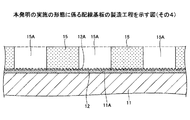
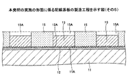
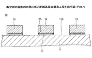
【解決手段】絶縁層11の平滑な上面11Aを覆うようにシード層12を形成し、次いで、シード層12の上面12Aを粗化し、その後、配線13の形成領域に対応する部分のシード層12の上面12Aを露出する開口部15Aを有しためっき用レジスト膜15を形成し、次いで、シード層12を給電層とする電解めっき法によりシード層12の上面12Aに配線13を形成し、次いで、めっき用レジスト膜15を除去し、その後、配線13が形成されていない部分の不要なシード層12を除去する。
【選択図】図9
Description
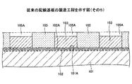
図9は、本発明の実施の形態に係る配線基板の断面図である。
続いて、粗化処理の有無とエッチング速度との関係について調査した結果を示す。始めに表1に示す4種類のサンプル(サンプル1〜4)を準備した。サンプル1〜4は、結果の再現性を確認するため、各2個ずつ作製した。

11 絶縁層
11A,12A 上面
12 シード層
13 配線
15 めっき用レジスト膜
15A 開口部
Claims (4)
- 平滑な上面を有する絶縁層と、前記絶縁層の前記平滑な上面に形成されたシード層と、前記シード層上に形成された配線と、を備えた配線基板の製造方法であって、
前記絶縁層の前記平滑な上面を覆うように、前記シード層を形成するシード層形成工程と、
前記シード層の上面を粗化するシード層粗化工程と、
前記シード層粗化工程後、前記配線の形成領域に対応する部分の前記シード層の上面を露出する開口部を有しためっき用レジスト膜を前記シード層の上面に形成するめっき用レジスト膜形成工程と、
前記シード層を給電層とする電解めっき法により、前記シード層の上面に前記配線を形成する配線形成工程と、
前記配線形成工程後に、前記めっき用レジスト膜を除去するめっき用レジスト膜除去工程と、
前記配線が形成されていない部分の不要な前記シード層を除去するシード層除去工程と、を含むことを特徴とする配線基板の製造方法。 - 前記シード層形成工程と前記シード層粗化工程とに代えて、前記絶縁層の前記平滑な上面を覆うように、前記シード層となる、上面に微細な針状の凹凸を有したCu−Ni−P合金からなる無電解めっき層を形成するCu−Ni−P合金層形成工程を有することを特徴とする請求項1記載の配線基板の製造方法。
- 前記シード層粗化工程では、前記シード層の上面の算術平均粗さRaが0.10μm≦Ra≦0.5μmとなるように粗化処理を行うことを特徴とする請求項1記載の配線基板の製造方法。
- 前記Cu−Ni−P合金層形成工程では、前記Cu−Ni−P合金層の上面の算術平均粗さRaが0.10μm≦Ra≦0.5μmとなるように無電解めっきを行うことを特徴とする請求項2記載の配線基板の製造方法。
Priority Applications (2)
| Application Number | Priority Date | Filing Date | Title |
|---|---|---|---|
| JP2008223635A JP2009260216A (ja) | 2008-03-19 | 2008-09-01 | 配線基板の製造方法 |
| US12/406,161 US20090238956A1 (en) | 2008-03-19 | 2009-03-18 | Manufacturing method of a wiring board containing a seed layer having a roughened surface |
Applications Claiming Priority (2)
| Application Number | Priority Date | Filing Date | Title |
|---|---|---|---|
| JP2008071583 | 2008-03-19 | ||
| JP2008223635A JP2009260216A (ja) | 2008-03-19 | 2008-09-01 | 配線基板の製造方法 |
Publications (2)
| Publication Number | Publication Date |
|---|---|
| JP2009260216A true JP2009260216A (ja) | 2009-11-05 |
| JP2009260216A5 JP2009260216A5 (ja) | 2011-09-15 |
Family
ID=41089180
Family Applications (1)
| Application Number | Title | Priority Date | Filing Date |
|---|---|---|---|
| JP2008223635A Pending JP2009260216A (ja) | 2008-03-19 | 2008-09-01 | 配線基板の製造方法 |
Country Status (2)
| Country | Link |
|---|---|
| US (1) | US20090238956A1 (ja) |
| JP (1) | JP2009260216A (ja) |
Cited By (3)
| Publication number | Priority date | Publication date | Assignee | Title |
|---|---|---|---|---|
| KR20150016090A (ko) * | 2013-08-01 | 2015-02-11 | 미쯔비시 가스 케미칼 컴파니, 인코포레이티드 | 프린트 배선판의 제조방법 |
| CN106469655A (zh) * | 2015-08-18 | 2017-03-01 | 中芯国际集成电路制造(上海)有限公司 | 凸块封装方法、半导体器件及电子装置 |
| WO2023012864A1 (ja) * | 2021-08-02 | 2023-02-09 | 昭和電工マテリアルズ株式会社 | 配線基板を製造する方法、及び配線基板 |
Families Citing this family (5)
| Publication number | Priority date | Publication date | Assignee | Title |
|---|---|---|---|---|
| US7969005B2 (en) * | 2007-04-27 | 2011-06-28 | Sanyo Electric Co., Ltd. | Packaging board, rewiring, roughened conductor for semiconductor module of a portable device, and manufacturing method therefor |
| JP5138459B2 (ja) * | 2008-05-15 | 2013-02-06 | 新光電気工業株式会社 | 配線基板の製造方法 |
| JP5511597B2 (ja) * | 2010-09-06 | 2014-06-04 | 日東電工株式会社 | 配線回路基板の製造方法 |
| US9361915B1 (en) * | 2011-12-02 | 2016-06-07 | Hutchinson Technology Incorporated | Method for making a disk drive head suspension component having a microstructured surface region |
| JP2021129048A (ja) * | 2020-02-14 | 2021-09-02 | イビデン株式会社 | 配線基板の製造方法及び配線基板 |
Citations (1)
| Publication number | Priority date | Publication date | Assignee | Title |
|---|---|---|---|---|
| JP2002151841A (ja) * | 2000-11-13 | 2002-05-24 | Ibiden Co Ltd | 多層プリント配線板の製造方法 |
Family Cites Families (5)
| Publication number | Priority date | Publication date | Assignee | Title |
|---|---|---|---|---|
| JPH0783168B2 (ja) * | 1988-04-13 | 1995-09-06 | 株式会社日立製作所 | プリント板の製造方法 |
| DE4231535C2 (de) * | 1991-09-20 | 1997-12-11 | Hitachi Ltd | Verfahren zur Erzeugung eines leitenden Schaltungsmusters |
| US5679230A (en) * | 1995-08-21 | 1997-10-21 | Oak-Mitsui, Inc. | Copper foil for printed circuit boards |
| MY125599A (en) * | 1996-12-19 | 2006-08-30 | Ibiden Co Ltd | Printed circuit boards and method of producing the same |
| JP4665531B2 (ja) * | 2005-01-27 | 2011-04-06 | 日立電線株式会社 | 配線板の製造方法 |
-
2008
- 2008-09-01 JP JP2008223635A patent/JP2009260216A/ja active Pending
-
2009
- 2009-03-18 US US12/406,161 patent/US20090238956A1/en not_active Abandoned
Patent Citations (1)
| Publication number | Priority date | Publication date | Assignee | Title |
|---|---|---|---|---|
| JP2002151841A (ja) * | 2000-11-13 | 2002-05-24 | Ibiden Co Ltd | 多層プリント配線板の製造方法 |
Cited By (11)
| Publication number | Priority date | Publication date | Assignee | Title |
|---|---|---|---|---|
| KR20150016090A (ko) * | 2013-08-01 | 2015-02-11 | 미쯔비시 가스 케미칼 컴파니, 인코포레이티드 | 프린트 배선판의 제조방법 |
| JP2015046575A (ja) * | 2013-08-01 | 2015-03-12 | 三菱瓦斯化学株式会社 | プリント配線板の製造方法 |
| TWI627884B (zh) * | 2013-08-01 | 2018-06-21 | Mitsubishi Gas Chemical Co | 印刷電路板之製造方法 |
| KR20190132959A (ko) * | 2013-08-01 | 2019-11-29 | 미쯔비시 가스 케미칼 컴파니, 인코포레이티드 | 프린트 배선판의 제조방법 |
| KR102052946B1 (ko) * | 2013-08-01 | 2019-12-06 | 미쯔비시 가스 케미칼 컴파니, 인코포레이티드 | 프린트 배선판의 제조방법 |
| KR102176434B1 (ko) | 2013-08-01 | 2020-11-09 | 미쯔비시 가스 케미칼 컴파니, 인코포레이티드 | 프린트 배선판의 제조방법 |
| KR20200127144A (ko) * | 2013-08-01 | 2020-11-10 | 미쯔비시 가스 케미칼 컴파니, 인코포레이티드 | 프린트 배선판의 제조방법 |
| KR102237844B1 (ko) | 2013-08-01 | 2021-04-09 | 미쯔비시 가스 케미칼 컴파니, 인코포레이티드 | 프린트 배선판의 제조방법 |
| CN106469655A (zh) * | 2015-08-18 | 2017-03-01 | 中芯国际集成电路制造(上海)有限公司 | 凸块封装方法、半导体器件及电子装置 |
| WO2023012864A1 (ja) * | 2021-08-02 | 2023-02-09 | 昭和電工マテリアルズ株式会社 | 配線基板を製造する方法、及び配線基板 |
| WO2023013556A1 (ja) * | 2021-08-02 | 2023-02-09 | 昭和電工マテリアルズ株式会社 | 配線基板を製造する方法、及び配線基板 |
Also Published As
| Publication number | Publication date |
|---|---|
| US20090238956A1 (en) | 2009-09-24 |
Similar Documents
| Publication | Publication Date | Title |
|---|---|---|
| JP2009260216A (ja) | 配線基板の製造方法 | |
| JP2003008199A (ja) | プリント配線基板の銅表面粗化方法ならびにプリント配線基板およびその製造方法 | |
| US11690178B2 (en) | Multilayer printed wiring board and method of manufacturing the same | |
| KR100899588B1 (ko) | 인쇄 회로 기판 제조에서 옥사이드 공정을 대체하고 미세라인을 제조하기 위해 구리 포일을 금속 처리하는 인쇄회로 기판 제조 방법 | |
| JP5483658B2 (ja) | 配線基板の製造方法 | |
| JP4195706B2 (ja) | プリント配線板およびその製造方法 | |
| JP2009188324A (ja) | 配線基板及びその製造方法 | |
| JP6065357B2 (ja) | プリント配線板の製造方法 | |
| JP2003078234A (ja) | プリント配線板およびその製造方法 | |
| JP2004095983A (ja) | プリント配線板の製造方法 | |
| JP2013162007A (ja) | 微細配線パターンの製造方法 | |
| JP2010087285A (ja) | 多層回路基板の製造方法 | |
| JP6511818B2 (ja) | プリント配線板の製造方法 | |
| KR100756751B1 (ko) | 미세회로용 동박 | |
| JP2004039771A (ja) | 配線回路基板の製造方法 | |
| JP4720521B2 (ja) | フレキシブル配線基板およびその製造方法 | |
| JP2004140085A (ja) | 回路基板及びその製造方法 | |
| JP5481586B1 (ja) | キャリア付銅箔、キャリア付銅箔の製造方法、プリント配線板、プリント回路板、銅張積層板、及びプリント配線板の製造方法 | |
| KR20030073919A (ko) | 단일 에칭 세미 애디티브 방식을 이용한 다층인쇄회로기판의 제조방법 | |
| KR100934106B1 (ko) | 미세 피치의 인쇄회로기판 제조를 위한 완전 부가 공법 | |
| KR20070113706A (ko) | 리드선 없이 인쇄 회로 기판에 전해 금도금을 수행하는 방법 | |
| JP4168798B2 (ja) | プリント配線板の製造方法 | |
| JP2010205803A (ja) | 配線基板の製造方法 | |
| JP2010040673A (ja) | 多層配線回路基板の製造方法 | |
| JP2020096005A (ja) | 半導体パッケージ基板 |
Legal Events
| Date | Code | Title | Description |
|---|---|---|---|
| A521 | Written amendment |
Free format text: JAPANESE INTERMEDIATE CODE: A523 Effective date: 20110803 |
|
| A621 | Written request for application examination |
Free format text: JAPANESE INTERMEDIATE CODE: A621 Effective date: 20110803 |
|
| A977 | Report on retrieval |
Free format text: JAPANESE INTERMEDIATE CODE: A971007 Effective date: 20120629 |
|
| A131 | Notification of reasons for refusal |
Free format text: JAPANESE INTERMEDIATE CODE: A131 Effective date: 20120703 |
|
| A02 | Decision of refusal |
Free format text: JAPANESE INTERMEDIATE CODE: A02 Effective date: 20121106 |