JP2009260216A - Method for manufacturing wiring board - Google Patents
Method for manufacturing wiring board Download PDFInfo
- Publication number
- JP2009260216A JP2009260216A JP2008223635A JP2008223635A JP2009260216A JP 2009260216 A JP2009260216 A JP 2009260216A JP 2008223635 A JP2008223635 A JP 2008223635A JP 2008223635 A JP2008223635 A JP 2008223635A JP 2009260216 A JP2009260216 A JP 2009260216A
- Authority
- JP
- Japan
- Prior art keywords
- seed layer
- wiring
- layer
- resist film
- plating
- Prior art date
- Legal status (The legal status is an assumption and is not a legal conclusion. Google has not performed a legal analysis and makes no representation as to the accuracy of the status listed.)
- Pending
Links
Images


Classifications
-
- H—ELECTRICITY
- H05—ELECTRIC TECHNIQUES NOT OTHERWISE PROVIDED FOR
- H05K—PRINTED CIRCUITS; CASINGS OR CONSTRUCTIONAL DETAILS OF ELECTRIC APPARATUS; MANUFACTURE OF ASSEMBLAGES OF ELECTRICAL COMPONENTS
- H05K3/00—Apparatus or processes for manufacturing printed circuits
- H05K3/10—Apparatus or processes for manufacturing printed circuits in which conductive material is applied to the insulating support in such a manner as to form the desired conductive pattern
- H05K3/108—Apparatus or processes for manufacturing printed circuits in which conductive material is applied to the insulating support in such a manner as to form the desired conductive pattern by semi-additive methods; masks therefor
-
- H—ELECTRICITY
- H05—ELECTRIC TECHNIQUES NOT OTHERWISE PROVIDED FOR
- H05K—PRINTED CIRCUITS; CASINGS OR CONSTRUCTIONAL DETAILS OF ELECTRIC APPARATUS; MANUFACTURE OF ASSEMBLAGES OF ELECTRICAL COMPONENTS
- H05K2201/00—Indexing scheme relating to printed circuits covered by H05K1/00
- H05K2201/03—Conductive materials
- H05K2201/0332—Structure of the conductor
- H05K2201/0335—Layered conductors or foils
- H05K2201/0344—Electroless sublayer, e.g. Ni, Co, Cd or Ag; Transferred electroless sublayer
-
- H—ELECTRICITY
- H05—ELECTRIC TECHNIQUES NOT OTHERWISE PROVIDED FOR
- H05K—PRINTED CIRCUITS; CASINGS OR CONSTRUCTIONAL DETAILS OF ELECTRIC APPARATUS; MANUFACTURE OF ASSEMBLAGES OF ELECTRICAL COMPONENTS
- H05K3/00—Apparatus or processes for manufacturing printed circuits
- H05K3/10—Apparatus or processes for manufacturing printed circuits in which conductive material is applied to the insulating support in such a manner as to form the desired conductive pattern
- H05K3/18—Apparatus or processes for manufacturing printed circuits in which conductive material is applied to the insulating support in such a manner as to form the desired conductive pattern using precipitation techniques to apply the conductive material
- H05K3/181—Apparatus or processes for manufacturing printed circuits in which conductive material is applied to the insulating support in such a manner as to form the desired conductive pattern using precipitation techniques to apply the conductive material by electroless plating
-
- H—ELECTRICITY
- H05—ELECTRIC TECHNIQUES NOT OTHERWISE PROVIDED FOR
- H05K—PRINTED CIRCUITS; CASINGS OR CONSTRUCTIONAL DETAILS OF ELECTRIC APPARATUS; MANUFACTURE OF ASSEMBLAGES OF ELECTRICAL COMPONENTS
- H05K3/00—Apparatus or processes for manufacturing printed circuits
- H05K3/38—Improvement of the adhesion between the insulating substrate and the metal
- H05K3/382—Improvement of the adhesion between the insulating substrate and the metal by special treatment of the metal
- H05K3/383—Improvement of the adhesion between the insulating substrate and the metal by special treatment of the metal by microetching
-
- H—ELECTRICITY
- H05—ELECTRIC TECHNIQUES NOT OTHERWISE PROVIDED FOR
- H05K—PRINTED CIRCUITS; CASINGS OR CONSTRUCTIONAL DETAILS OF ELECTRIC APPARATUS; MANUFACTURE OF ASSEMBLAGES OF ELECTRICAL COMPONENTS
- H05K3/00—Apparatus or processes for manufacturing printed circuits
- H05K3/38—Improvement of the adhesion between the insulating substrate and the metal
- H05K3/382—Improvement of the adhesion between the insulating substrate and the metal by special treatment of the metal
- H05K3/384—Improvement of the adhesion between the insulating substrate and the metal by special treatment of the metal by plating
Landscapes
- Engineering & Computer Science (AREA)
- Manufacturing & Machinery (AREA)
- Microelectronics & Electronic Packaging (AREA)
- Manufacturing Of Printed Wiring (AREA)
Abstract
Description
本発明は、配線基板の製造方法に関し、特に、絶縁層上に配置されたシード層上にめっき用レジスト膜を設け、シード層を給電層とする電解めっき法により、シード層上に配線を形成する配線基板の製造方法に関する。 The present invention relates to a method of manufacturing a wiring board, and in particular, a resist film for plating is provided on a seed layer disposed on an insulating layer, and wiring is formed on the seed layer by an electrolytic plating method using the seed layer as a power feeding layer. The present invention relates to a method for manufacturing a wiring board.
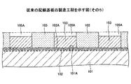
図1は、従来の配線基板の断面図である。 FIG. 1 is a cross-sectional view of a conventional wiring board.
図1を参照するに、従来の配線基板100は、絶縁層101と、シード層102と、配線103とを有する。絶縁層101の上面101Aは、粗化処理されている。これにより、絶縁層101の上面101Aには、微細な凹凸が形成されている。この微細な凹凸は、絶縁層101の上面101Aに形成されるシード層102の上面102Aに微細な凹凸を形成(具体的には、微細な凹凸を転写)するためのものである。絶縁層101の上面101Aの算術平均粗さRaは、例えば、0.5μm以上とすることができる。絶縁層101としては、例えば、樹脂層を用いることができる。
Referring to FIG. 1, a
シード層102は、配線103の形成領域に対応する部分の絶縁層101の上面101Aに形成されている。シード層102の下部は、絶縁層101の上面101Aに形成された微細な凹部に入り込むように形成されている。シード層102の上面102Aには、微細な凹凸が形成されている。シード層102は、電解めっき法により配線103を形成する際、給電層として使用する層である。シード層102としては、例えば、Cu層を用いることができる。シード層102としてCu層を用いた場合、シード層102の厚さは、例えば、1μmとすることができる。
The
配線103は、シード層102上に設けられている。配線103は、例えば、シード層102を給電層とする電気めっき法により、シード層102の上面102AにCuめっき膜を析出成長させることで形成する。
The
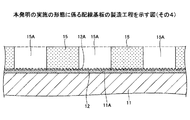
図2〜図8は、従来の配線基板の製造工程を示す図である。図2〜図8において、従来の配線基板100と同一構成部分には同一符号を付す。
2 to 8 are views showing a manufacturing process of a conventional wiring board. 2-8, the same code | symbol is attached | subjected to the same component as the
図2〜図8を参照して、従来の配線基板100の製造方法について説明する。始めに、図2に示す工程では、絶縁層101を形成する。この段階では、絶縁層101の表面101Aは、平滑な面とされている。
With reference to FIGS. 2-8, the manufacturing method of the
次いで、図3に示す工程では、図2に示す絶縁層101の上面101Aの粗化処理(例えば、デスミア処理)を行う。この工程では、絶縁層101の上面101Aの算術平均粗さRaが0.5μm程度となるように、絶縁層101の上面101Aの粗化処理を行う。これにより、絶縁層101の上面101Aに微細な凹凸が形成される。
Next, in the process shown in FIG. 3, a roughening process (for example, a desmear process) is performed on the
次いで、図4に示す工程では、図3に示す絶縁層101の上面101Aを覆うように、シード層102を形成する。このとき、絶縁層101の上面101Aに形成された微細な凹凸が、シード層102に転写されるため、シード層102の上面102A側に微細な凹凸が形成される。また、シード層102の下部は、絶縁層101の上面101Aに形成された微細な凹部に入り込むように形成される。シード層102としては、例えば、Cu層を用いることができる。
Next, in a step shown in FIG. 4, a
次いで、図5に示す工程では、シード層102の上面102Aにめっき用レジスト膜105を形成する。めっき用レジスト膜105は、配線103の形成領域に対応する部分のシード層102の上面102Aを露出する開口部105Aを有する。
Next, in a step shown in FIG. 5, a plating
このように、シード層102の上面102A側に微細な凹凸を形成することにより、シード層102とめっき用レジスト膜105との間の密着性を向上させることができる。
Thus, by forming fine irregularities on the
次いで、図6に示す工程では、シード層102を給電層とする電解めっき法により、微細な凹凸が形成されたシード層102の上面102A側にCuめっき膜を析出成長させることで、配線105を形成する。このとき、めっき用レジスト膜105の下部は、シード層102の上面側に形成された微細な凹凸の凹部に入り込むように形成されている。そのため、めっき液がシード層102とめっき用レジスト膜105との間に侵入して、めっき用レジスト膜105が剥がれることを防止できる。
Next, in the process shown in FIG. 6, a Cu plating film is deposited and grown on the
次いで、図7に示す工程では、図6に示すめっき用レジスト膜105を除去する。次いで、図8に示す工程では、Cuをエッチングするエッチング液に図7に示す構造体を浸漬させることで、配線105に覆われていない部分のシード層102を除去する。これにより、従来の配線基板100が製造される(例えば、特許文献1参照。)。
しかしながら、従来の配線基板100では、微細な凹凸が形成された絶縁層101の上面101Aにシード層102を形成していたため、図8に示す工程において、絶縁層101の上面101A側の微細な凹部に形成された不要なシード層102を、エッチングにより除去するために多くの時間(エッチング時間)が必要となってしまう。
However, in the
これにより、シード層102を除去するためのエッチング液により、配線103がエッチングされて、不要な部分のシード層102を除去後の配線105のサイズが所定のサイズ(具体的には、設計上の配線105の幅及び厚さ)よりも小さくなってしまうという問題があった。特に、配線幅の狭い配線105(例えば、配線幅が10μm以下の配線)を形成する場合に、上記問題は大きな問題となる。
As a result, the
そこで本発明は、上述した問題点に鑑みなされたものであり、シード層上に形成されるめっき用レジスト膜の剥がれを防止できると共に、不要なシード層を除去する際のエッチング時間を短縮することが可能となり、シード層除去工程後の配線のサイズが所定のサイズとなるように配線を形成することができる配線基板の製造方法を提供することを目的とする。 Therefore, the present invention has been made in view of the above-described problems, and can prevent peeling of the plating resist film formed on the seed layer and shorten the etching time when removing the unnecessary seed layer. An object of the present invention is to provide a method of manufacturing a wiring board that can form a wiring so that the size of the wiring after the seed layer removing step becomes a predetermined size.
本発明の一観点によれば、平滑な上面を有する絶縁層と、前記絶縁層の前記平滑な上面に形成されたシード層と、前記シード層上に形成された配線と、を備えた配線基板の製造方法であって、前記絶縁層の前記平滑な上面を覆うように、前記シード層を形成するシード層形成工程と、前記シード層の上面を粗化するシード層粗化工程と、前記シード層粗化工程後、前記配線の形成領域に対応する部分の前記シード層の上面を露出する開口部を有しためっき用レジスト膜を前記シード層の上面に形成するめっき用レジスト膜形成工程と、前記シード層を給電層とする電解めっき法により、前記シード層の上面に前記配線を形成する配線形成工程と、前記配線形成工程後に、前記めっき用レジスト膜を除去するめっき用レジスト膜除去工程と、前記配線が形成されていない部分の不要な前記シード層を除去するシード層除去工程と、を含むことを特徴とする配線基板の製造方法が提供される。 According to one aspect of the present invention, a wiring board comprising: an insulating layer having a smooth upper surface; a seed layer formed on the smooth upper surface of the insulating layer; and a wiring formed on the seed layer. A seed layer forming step of forming the seed layer so as to cover the smooth upper surface of the insulating layer, a seed layer roughening step of roughening the upper surface of the seed layer, and the seed After the layer roughening step, a plating resist film forming step of forming a plating resist film having an opening exposing the upper surface of the seed layer in a portion corresponding to the wiring formation region on the upper surface of the seed layer; A wiring forming step of forming the wiring on an upper surface of the seed layer by an electrolytic plating method using the seed layer as a power feeding layer; and a plating resist film removing step of removing the plating resist film after the wiring forming step; ,in front Method for manufacturing a wiring board, which comprises a seed layer removing step of removing unnecessary the seed layer portion wirings is not formed is provided.
本発明によれば、絶縁層の平滑な上面を覆うようにシード層を形成し、次いで、シード層の上面を粗化し、その後、配線の形成領域に対応する部分のシード層の上面を露出する開口部を有しためっき用レジスト膜をシード層の上面に形成することにより、シード層からめっき用レジスト膜が剥がれることを防止できる。 According to the present invention, the seed layer is formed so as to cover the smooth upper surface of the insulating layer, and then the upper surface of the seed layer is roughened, and then the upper surface of the seed layer corresponding to the formation region of the wiring is exposed. By forming the plating resist film having the opening on the upper surface of the seed layer, it is possible to prevent the plating resist film from being peeled off from the seed layer.
また、シード層粗化工程後、配線の形成領域に対応する部分のシード層の上面を露出する開口部を有しためっき用レジスト膜をシード層の上面に形成し、次いで、シード層を給電層とする電解めっき法により、シード層の上面に配線を形成し、次いで、めっき用レジスト膜を除去し、その後、配線が形成されていない部分の不要なシード層を除去することにより、例えば、不要な部分のシード層をエッチング液により除去する際、従来よりも短時間で不要な部分のシード層を除去することが可能となる。これにより、シード層除去工程において、配線がエッチングされにくくなるため、シード層除去工程後の配線のサイズが所定のサイズ(具体的には、設計上の配線の厚さ及び配線幅)となるように配線を形成することができる。 Further, after the seed layer roughening step, a resist film for plating having an opening that exposes the upper surface of the seed layer corresponding to the formation region of the wiring is formed on the upper surface of the seed layer, and then the seed layer is formed as the power supply layer. By forming the wiring on the upper surface of the seed layer by the electrolytic plating method, and then removing the plating resist film, and then removing the unnecessary seed layer in the portion where the wiring is not formed, for example, unnecessary When removing a part of the seed layer with an etching solution, an unnecessary part of the seed layer can be removed in a shorter time than in the prior art. This makes it difficult for the wiring to be etched in the seed layer removal step, so that the size of the wiring after the seed layer removal step becomes a predetermined size (specifically, the thickness and width of the designed wiring). Wiring can be formed on the substrate.
本発明によれば、シード層上に形成されるめっき用レジスト膜の剥がれを防止できると共に、不要なシード層を除去する際のエッチング時間を短縮することが可能となり、シード層除去工程後の配線のサイズが所定のサイズとなるように配線を形成することができる。 According to the present invention, the plating resist film formed on the seed layer can be prevented from being peeled off, and the etching time when removing the unnecessary seed layer can be shortened. The wirings can be formed so that the size of each becomes a predetermined size.
次に、図面に基づいて本発明の実施の形態について説明する。 Next, embodiments of the present invention will be described with reference to the drawings.
(実施の形態)
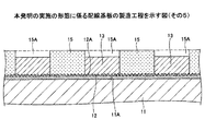
図9は、本発明の実施の形態に係る配線基板の断面図である。
(Embodiment)
FIG. 9 is a cross-sectional view of the wiring board according to the embodiment of the present invention.
図9を参照するに、本実施の形態の配線基板10は、絶縁層11と、シード層12と、配線13とを有する。配線基板10としては、例えば、コアレス基板やコア付きビルドアップ基板等を用いることができる。なお、図9では、配線基板10の主要部のみ図示する。
Referring to FIG. 9, the
絶縁層11は、シード層12を形成するための層である。絶縁層11の上面11Aは、従来の絶縁層101の上面101Aよりも平滑な面(例えば、算術平均粗さRaがRa≦0.4μmとなるような面)とされている。
The
このように、絶縁層11の上面11Aを平滑な面とすることにより、不要な部分のシード層21を除去する際(後述する図16に示す工程参照)、従来よりも短時間で不要な部分のシード層21を除去することが可能となるので、シード層除去工程後の配線13のサイズが所定のサイズとなるように配線13を形成することができる。
As described above, when the
絶縁層11としては、例えば、樹脂層を用いることができる。また、樹脂層の材料としては、例えば、エポキシ樹脂やポリイミド樹脂等を用いることができる。
As the insulating
シード層12は、配線13の形成領域に対応する部分の絶縁層11の上面11Aに設けられている。シード層12は、電解めっき法により配線13を形成する際の給電層である。シード層12の上面12Aには、配線13を形成するためのめっき用レジスト膜15(後述する図13参照)が形成される。シード層12の上面12Aは、粗化された面であり、微細な凹凸が形成されている。シード層12の上面12Aの算術平均粗さRaは、例えば、Ra≧0.10μmとすることができる。
The
このように、シード層12の上面12Aの算術平均粗さRaをRa≧0.10μmにすることにより、配線13を形成するためのめっき用レジスト膜15がシード層12から剥がれることを防止できる。なお、シード層12の上面12Aの算術平均粗さRaがRa<0.10μmの場合、配線13を形成するためのめっき用レジスト膜15がシード層12から剥がれてしまう。
Thus, by setting the arithmetic average roughness Ra of the
又、シード層12の上面12Aの算術平均粗さRaをRa≧0.10μmにすることにより、従来の配線基板100のシード層102と比較して、シード層12の表面積が大きくなる。そのため、シード層12の方が、不要なシード層12を除去する際に、エッチング液と反応する面積が大きくなり、エッチング液と反応する量が増える。その結果、シード層102とシード層12が同じ質量であるとすると、シード層12の方がエッチング時間を短縮することが可能となり、シード層12以外の部分(配線13等)の不要なエッチングを抑えることができる。配線13の不要なエッチングが抑えられるため、特に、配線幅の狭い配線13(具体的には、配線幅が10μm以下の配線13)を形成する際に有効である。
Further, by setting the arithmetic average roughness Ra of the
また、好ましくは、例えば、シード層12の上面12Aの算術平均粗さRaを0.10μm≦Ra≦0.5μmにするとよい。
Preferably, for example, the arithmetic average roughness Ra of the
このように、シード層12の上面12Aの算術平均粗さRaを0.10μm≦Ra≦0.5μmにすることにより、配線幅の狭い配線13(例えば、配線幅が10μm以下の配線13)を精度良く形成することが可能となる。なお、シード層12の上面12Aの算術平均粗さRaがRa>0.5μmの場合、配線幅の狭い配線13(具体的には、配線幅が10μm以下の配線13)を精度良く形成することが困難となる。
Thus, by setting the arithmetic average roughness Ra of the
シード層12としては、例えば、Cu層を用いることができる。シード層12としてCu層を用いた場合、上面12Aが粗化されたシード層12の厚さは、例えば、1μmとすることができる。
As the
配線13は、粗化されたシード層12の上面12Aに設けられている。配線13の材料としては、例えば、Cuを用いることができる。
The
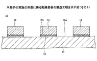
図10〜図16は、本発明の実施の形態に係る配線基板の製造工程を示す図である。図10〜図16において、本実施の形態の配線基板10と同一構成部分には、同一符号を付す。
10-16 is a figure which shows the manufacturing process of the wiring board based on embodiment of this invention. 10-16, the same code | symbol is attached | subjected to the same component as the
図10〜図16を参照して、本実施の形態の配線基板10の製造方法について説明する。始めに、図10に示す工程では、上面11Aが平滑化された絶縁層11を形成する。絶縁層11としては、例えば、樹脂層を用いることができる。また、樹脂層としては、例えば、エポキシ樹脂やポリイミド樹脂等を用いることができる。具体的には、例えば、絶縁層11として樹脂層を用いる場合、半硬化状態とされた樹脂フィルムをラミネートし、その後、樹脂フィルムを硬化させることで樹脂層を形成する。絶縁層11の上面11Aは、従来の粗化された絶縁層101の上面101Aよりも平滑な面(例えば、算術平均粗さRaがRa≦0.4μmの面)とされている。
With reference to FIGS. 10-16, the manufacturing method of the
このように、絶縁層11の上面11Aを平滑な面とすることにより、後述する図16に示す工程(シード層除去工程)において、エッチング液により不要な部分のシード層21を除去する際、従来よりも短時間でシード層21を除去することが可能となる。これにより、後述する図16に示す工程(シード層除去工程)において、配線13がエッチングされにくくなるため、所定のサイズ(具体的には、所定の配線13の幅及び厚さ)となるように配線13を形成することができる。なお、所定の配線13の幅とは、設計上の配線13の幅のことである。また、所定の配線13の厚さとは、設計上の配線13の厚さのことである。
In this way, by making the
次いで、図11に示す工程では、平滑な面とされた絶縁層11の上面11Aを覆うようにシード層12を形成する(シード層形成工程)。具体的には、例えば、無電解めっき法、スパッタ法、蒸着法等の方法によりシード層12を形成する。この段階では、シード層12の上面12Aは、平滑な面とされている。シード層12としては、例えば、Cu層を用いることができる。
Next, in the step shown in FIG. 11, the
また、この段階でのシード層12の厚さは、後述する図12に示す工程(シード層粗化工程)におけるシード層12の膜減りを考慮して、先に説明した図9に示すシード層12の厚さよりも厚くなるように設定するとよい。
Further, the thickness of the
具体的には、シード層12としてCu層を用いると共に、図9に示すシード層12の厚さが1μmの場合、シード層形成工程におけるシード層12の厚さは、例えば、2μm〜3μmとすることができる。
Specifically, when a Cu layer is used as the
次いで、図12に示す工程では、図11に示すシード層12の上面12Aを粗化する(シード層粗化工程)。具体的には、シード層12の粗化は、例えば、シード層12の上面12Aをエッチング(例えば、エッチング液を噴霧器から霧状に噴き出させることで行うエッチング)、或いはシード層12の上面12Aをブラスト処理することで行う。これにより、シード層12の上面12Aに微細な凹凸が形成される。エッチング液の噴霧によりシード層12の上面12Aの粗化処理を行う場合、エッチング液としては、例えば、CZ−8101(メック株式会社製)を用いることができる。CZ−8101(メック株式会社製)は、10%以下のギ酸を含んだエッチング液である。エッチング液としてCZ−8101(メック株式会社製)を用いた場合、噴霧器からエッチング液を噴霧させる際の圧力としては、例えば、0.2MPaを用いることができる。この場合の処理温度は、例えば、30℃を用いることができ、処理時間は、例えば、30秒〜60秒とすることができる。
Next, in the step shown in FIG. 12, the
シード層粗化工程では、シード層12の上面12Aの算術平均粗さRaがRa≧0.10μmとなるように粗化処理を行う。
In the seed layer roughening step, the roughening process is performed so that the arithmetic average roughness Ra of the
このように、シード層12の上面12Aの算術平均粗さRaをRa≧0.10μmにすることにより、シード層12の上面12Aに形成されるめっき用レジスト膜15(後述する図13参照)とシード層12との密着性が向上するため、めっき用レジスト膜15がシード層12から剥がれることを防止できる。なお、シード層12の上面12Aの算術平均粗さRaがRa<0.10μmの場合、めっき用レジスト膜15とシード層12との密着性が不十分となるため、シード層12からめっき用レジスト膜15が剥がれてしまう。
Thus, by setting the arithmetic average roughness Ra of the
また、好ましくは、シード層12の上面12Aの算術平均粗さRaを、例えば、0.10μm≦Ra≦0.5μmにするとよい。
Preferably, the arithmetic average roughness Ra of the
このように、シード層12の上面12Aの算術平均粗さRaを0.10μm≦Ra≦0.5μmにすることにより、配線幅の狭い配線13(例えば、配線幅が10μm以下の配線13)を精度良く形成することが可能となる。なお、シード層12の上面12Aの算術平均粗さRaがRa>0.5μmの場合、配線幅の狭い配線13(具体的には、配線幅が10μm以下の配線13)を精度良く形成することが困難となる。
Thus, by setting the arithmetic average roughness Ra of the
シード層12としては、例えば、Cu層を用いることができる。シード層12としてCu層を用いた場合、粗化処理後のシード層12の厚さは、例えば、1μmとすることができる。
As the
なお、上記説明したエッチングの代わりに、ブラスト処理(例えば、サンドブラスト処理)により、シード層12の上面12Aの算術平均粗さRaがRa≧0.10μmとなるように、シード層12の上面12Aを粗化してもよい。この場合、エッチングによりシード層12の上面12Aを粗化した場合と同様な効果を得ることができる。
Instead of the etching described above, the
次いで、図13に示す工程では、粗化処理されたシード層12の上面12Aに、開口部15Aを有しためっき用レジスト膜15を形成する(めっき用レジスト膜形成工程)。このとき、めっき用レジスト膜15の下部は、シード層12の上面12A側に形成された微細な凹部に入り込むように形成される。開口部15Aは、配線13の形成領域に対応する部分のシード層12の上面12A(粗化された上面)を露出するように形成する。
Next, in a step shown in FIG. 13, a plating resist
このように、粗化されたシード層12の上面12Aにめっき用レジスト膜15を形成することにより、シード層12とめっき用レジスト膜15との密着性が向上するため、シード層12からめっき用レジスト膜15が剥がれることを防止できる。
Thus, by forming the plating resist
次いで、図14に示す工程では、シード層12を給電層とする電解めっき法により、シード層12の上面12Aにめっき膜を析出成長させることで、めっき膜を母材とする配線13を形成する(配線形成工程)。この際、めっき用レジスト膜15の下部が微細な凹凸形状を有したシード層12の上面12Aの形状に追従するように形成されているため、シード層12とめっき用レジスト膜15との界面に、配線13を形成する際のめっき液が侵入することが抑制され、シード層12からめっき用レジスト膜15が剥がれることを防止できる。配線13の母材となるめっき膜としては、例えば、Cuめっき膜を用いることができる。
Next, in the step shown in FIG. 14, a plating film is deposited on the
次いで、図15に示す工程では、図14に示す構造体に設けられためっき用レジスト膜15を除去する(めっき用レジスト膜除去工程)。次いで、図16に示す工程では、配線13に覆われていない部分のシード層12(不要な部分のシード層12)を除去する(シード層除去工程)。具体的には、例えば、エッチング液を用いたウエットエッチングにより、不要な部分のシード層12を除去する。シード層除去工程で使用するエッチング液としては、例えば、硫酸・過酸化水素系のエッチング液を用いることができる。これにより、本実施の形態の配線基板10が製造される。この際、先に説明したように、シード層12は、平滑な面とされた絶縁層11の上面11Aに形成されているため、従来よりも短時間のエッチング時間で不要な部分のシード層12を除去することが可能となるので、シード層除去工程後の配線13のサイズが所定のサイズ(具体的には、設計上の配線13の厚さ及び配線幅)となるように配線13を形成することができる。
Next, in the step shown in FIG. 15, the plating resist
又、先に説明したように、従来の配線基板100のシード層102と比較して、シード層12の表面積が大きいため、エッチング液と反応する面積が大きくなり、エッチング液と反応する量が増える。その結果、シード層102とシード層12が同じ質量であるとすると、シード層12の方がエッチング時間を短縮することが可能となり、シード層12以外の部分(配線13等)の不要なエッチングを抑えることができる。配線13の不要なエッチングが抑えられるため、特に、配線幅の狭い配線13(具体的には、配線幅が10μm以下の配線13)を形成する際に有効である。
Further, as described above, since the surface area of the
本実施の形態の配線基板の製造方法によれば、絶縁層11の平滑な上面11Aを覆うようにシード層12を形成し、次いで、シード層12の上面12Aを粗化し、その後、配線13の形成領域に対応する部分のシード層12の上面12Aを露出する開口部15Aを有しためっき用レジスト膜15をシード層12の上面12Aに形成することにより、シード層12からめっき用レジスト膜15が剥がれることを防止できる。
According to the method for manufacturing a wiring substrate of the present embodiment, the
また、シード層粗化工程後、配線13の形成領域に対応する部分のシード層12の上面を露出する開口部15Aを有しためっき用レジスト膜15をシード層12の上面12Aに形成し、次いで、シード層12を給電層とする電解めっき法により、シード層12の上面12Aに配線を形成し、次いで、めっき用レジスト膜15を除去し、その後、配線13が形成されていない部分の不要なシード層12を除去することにより、例えば、不要な部分のシード層12をエッチング液により除去する際、従来よりも短時間で不要な部分のシード層12を除去することが可能となるため、シード層除去工程後の配線13のサイズが所定のサイズ(具体的には、設計上の配線13の厚さ及び配線幅)となるように配線13を形成することができる。
Also, after the seed layer roughening step, a plating resist
又、シード層12の上面12Aの算術平均粗さRaをRa≧0.10μmにすることにより、従来の配線基板100のシード層102と比較して、シード層12の表面積が大きくなる。そのため、シード層12の方が、不要なシード層12を除去する際に、エッチング液と反応する面積が大きくなり、エッチング液と反応する量が増える。その結果、シード層102とシード層12が同じ質量であるとすると、シード層12の方がエッチング時間を短縮することが可能となり、シード層12以外の部分(配線13等)の不要なエッチングを抑えることができる。配線13の不要なエッチングが抑えられるため、特に、配線幅の狭い配線13(具体的には、配線幅が10μm以下の配線13)を形成する際に有効である。
Further, by setting the arithmetic average roughness Ra of the
なお、本実施の形態で説明したシード層形成工程及びシード層粗化工程の代わりに、絶縁層11の平滑な上面11Aに、無電解めっき法を用いて針状とされたシード層12を形成してもよい。針状とされたシード層12としては、例えば、Cuが90wt%〜96wt%、Niが1wt%〜5wt%、Pが0.5wt%〜2wt%を含んだCu−Ni−P合金からなる無電解めっき層(Cu−Ni−P合金層)を用いるとよい。このような組成とされたCu−Ni−P合金をシード層12として用いることで、無電解めっき法により形成されるシード層12(Cu−Ni−P合金層)の上面側に微細な針状の凹凸を形成することができる。
In addition, instead of the seed layer forming step and the seed layer roughening step described in the present embodiment, a needle-
シード層12(Cu−Ni−P合金層)の上面12Aの算術平均粗さRaは、例えば、Ra≧0.10μmとすることができる。また、好ましくは、例えば、シード層12(Cu−Ni−P合金層)の上面12Aの算術平均粗さRaを0.10μm≦Ra≦0.5μmにするとよい。このようにすることにより、先に説明した効果と同様の効果を奏する。
The arithmetic average roughness Ra of the
(粗化処理とエッチング速度との関係)
続いて、粗化処理の有無とエッチング速度との関係について調査した結果を示す。始めに表1に示す4種類のサンプル(サンプル1〜4)を準備した。サンプル1〜4は、結果の再現性を確認するため、各2個ずつ作製した。
(Relationship between roughening treatment and etching rate)
Then, the result of having investigated about the relationship between the presence or absence of a roughening process and an etching rate is shown. First, four types of samples (

サンプル1は、シード層12に相当する層として無電解銅めっきを用い、その上面に対して粗化処理を行っていないものであり、上面の算術平均粗さRaは0.07μmである。サンプル2は、シード層12に相当する層としてとして無電解銅めっきを用い、その上面に対して粗化処理を行ったものであり、上面の算術平均粗さRaは0.31μmである。サンプル3は、シード層12に相当する層としてとして電解銅箔を用い、その上面に対して粗化処理を行っていないものであり、上面の算術平均粗さRaは0.09μmである。サンプル4は、シード層12に相当する層としてとして電解銅箔を用い、その上面に対して粗化処理を行ったものであり、上面の算術平均粗さRaは0.24μmである。
なお、粗化処理は、エッチング液としてCZ−8101(メック株式会社製)を用い、噴霧器からエッチング液を噴霧させる際の圧力は0.2MPa、処理温度は30℃、処理時間は30秒〜60秒とした。又、表1に示す算術平均粗さRaは、レーザー顕微鏡を用いて測定した。 The roughening treatment uses CZ-8101 (manufactured by MEC Co., Ltd.) as an etching solution, the pressure when spraying the etching solution from the sprayer is 0.2 MPa, the treatment temperature is 30 ° C., and the treatment time is 30 seconds to 60 seconds. Seconds. The arithmetic average roughness Ra shown in Table 1 was measured using a laser microscope.
図17は、サンプル1〜4の各条件におけるエッチング膜厚を例示する図である。図17において、FE条件とはフラッシュエッチ条件(=エッチング時間)であり、サンプル1〜4について、1.5m/min及び2.0m/minの2種類のFE条件でエッチングを行った。図17において、サンプル1とサンプル2を比較すると、FE条件に依存せず、サンプル2の方がエッチングされる膜厚が厚いことがわかる。又、サンプル3とサンプル4を比較すると、FE条件に依存せず、サンプル4の方がエッチングされる膜厚が厚いことがわかる。すなわち、無電解銅めっき及び電解銅箔の何れについても、粗化処理有の方がエッチングされる膜厚が厚い(エッチング速度が速い)ことがわかる。粗化処理有の場合のエッチング速度は、粗化処理無の場合のエッチング速度よりも1.2〜1.3倍程度速くなっている。
FIG. 17 is a diagram illustrating an etching film thickness under each condition of
この結果は、粗化処理をすることにより、銅の表面積が大きくなり、エッチング液と反応する面積が増えたためと考えられる。これにより、単位時間当たりのエッチング量は、粗化処理された銅の表面の方が多くなり、エッチング時間を短縮することができると推察される。このように、粗化処理をすることにより、エッチング時間を短縮することが可能となり、不要なエッチングを抑えることができることが確認された。 This result is thought to be because the surface area of the copper increased due to the roughening treatment, and the area that reacted with the etching solution increased. Thereby, it is surmised that the etching amount per unit time is larger on the roughened copper surface, and the etching time can be shortened. As described above, it was confirmed that the roughening treatment can shorten the etching time and suppress unnecessary etching.
以上、本発明の好ましい実施の形態について詳述したが、本発明はかかる特定の実施の形態に限定されるものではなく、特許請求の範囲内に記載された本発明の要旨の範囲内において、種々の変形・変更が可能である。 The preferred embodiments of the present invention have been described in detail above, but the present invention is not limited to such specific embodiments, and within the scope of the present invention described in the claims, Various modifications and changes are possible.
本発明は、絶縁層上に配置されたシード層上にめっき用レジスト膜を設け、シード層を給電層とする電解めっき法により、シード層上に配線を形成する配線基板の製造方法に適用できる。 The present invention can be applied to a method of manufacturing a wiring substrate in which a plating resist film is provided on a seed layer disposed on an insulating layer, and wiring is formed on the seed layer by an electrolytic plating method using the seed layer as a power feeding layer. .
10 配線基板
11 絶縁層
11A,12A 上面
12 シード層
13 配線
15 めっき用レジスト膜
15A 開口部
DESCRIPTION OF
Claims (4)
前記絶縁層の前記平滑な上面を覆うように、前記シード層を形成するシード層形成工程と、
前記シード層の上面を粗化するシード層粗化工程と、
前記シード層粗化工程後、前記配線の形成領域に対応する部分の前記シード層の上面を露出する開口部を有しためっき用レジスト膜を前記シード層の上面に形成するめっき用レジスト膜形成工程と、
前記シード層を給電層とする電解めっき法により、前記シード層の上面に前記配線を形成する配線形成工程と、
前記配線形成工程後に、前記めっき用レジスト膜を除去するめっき用レジスト膜除去工程と、
前記配線が形成されていない部分の不要な前記シード層を除去するシード層除去工程と、を含むことを特徴とする配線基板の製造方法。 A method of manufacturing a wiring board comprising: an insulating layer having a smooth upper surface; a seed layer formed on the smooth upper surface of the insulating layer; and a wiring formed on the seed layer,
A seed layer forming step of forming the seed layer so as to cover the smooth upper surface of the insulating layer;
A seed layer roughening step for roughening an upper surface of the seed layer;
After the seed layer roughening step, a plating resist film forming step of forming on the upper surface of the seed layer a plating resist film having an opening exposing the upper surface of the seed layer in a portion corresponding to the wiring formation region When,
A wiring forming step of forming the wiring on an upper surface of the seed layer by an electrolytic plating method using the seed layer as a power feeding layer;
After the wiring formation step, a plating resist film removal step for removing the plating resist film;
And a seed layer removing step of removing the unnecessary seed layer in a portion where the wiring is not formed.
Priority Applications (2)
| Application Number | Priority Date | Filing Date | Title |
|---|---|---|---|
| JP2008223635A JP2009260216A (en) | 2008-03-19 | 2008-09-01 | Method for manufacturing wiring board |
| US12/406,161 US20090238956A1 (en) | 2008-03-19 | 2009-03-18 | Manufacturing method of a wiring board containing a seed layer having a roughened surface |
Applications Claiming Priority (2)
| Application Number | Priority Date | Filing Date | Title |
|---|---|---|---|
| JP2008071583 | 2008-03-19 | ||
| JP2008223635A JP2009260216A (en) | 2008-03-19 | 2008-09-01 | Method for manufacturing wiring board |
Publications (2)
| Publication Number | Publication Date |
|---|---|
| JP2009260216A true JP2009260216A (en) | 2009-11-05 |
| JP2009260216A5 JP2009260216A5 (en) | 2011-09-15 |
Family
ID=41089180
Family Applications (1)
| Application Number | Title | Priority Date | Filing Date |
|---|---|---|---|
| JP2008223635A Pending JP2009260216A (en) | 2008-03-19 | 2008-09-01 | Method for manufacturing wiring board |
Country Status (2)
| Country | Link |
|---|---|
| US (1) | US20090238956A1 (en) |
| JP (1) | JP2009260216A (en) |
Cited By (3)
| Publication number | Priority date | Publication date | Assignee | Title |
|---|---|---|---|---|
| KR20150016090A (en) * | 2013-08-01 | 2015-02-11 | 미쯔비시 가스 케미칼 컴파니, 인코포레이티드 | Method for preparing printed circuit board |
| CN106469655A (en) * | 2015-08-18 | 2017-03-01 | 中芯国际集成电路制造(上海)有限公司 | Projection method for packing, semiconductor device and electronic installation |
| WO2023012864A1 (en) * | 2021-08-02 | 2023-02-09 | 昭和電工マテリアルズ株式会社 | Method for manufacturing wiring board, and wiring board |
Families Citing this family (5)
| Publication number | Priority date | Publication date | Assignee | Title |
|---|---|---|---|---|
| US7969005B2 (en) * | 2007-04-27 | 2011-06-28 | Sanyo Electric Co., Ltd. | Packaging board, rewiring, roughened conductor for semiconductor module of a portable device, and manufacturing method therefor |
| JP5138459B2 (en) * | 2008-05-15 | 2013-02-06 | 新光電気工業株式会社 | Wiring board manufacturing method |
| JP5511597B2 (en) * | 2010-09-06 | 2014-06-04 | 日東電工株式会社 | Method for manufacturing printed circuit board |
| US9361915B1 (en) * | 2011-12-02 | 2016-06-07 | Hutchinson Technology Incorporated | Method for making a disk drive head suspension component having a microstructured surface region |
| JP2021129048A (en) * | 2020-02-14 | 2021-09-02 | イビデン株式会社 | Wiring board production method and wiring board |
Citations (1)
| Publication number | Priority date | Publication date | Assignee | Title |
|---|---|---|---|---|
| JP2002151841A (en) * | 2000-11-13 | 2002-05-24 | Ibiden Co Ltd | Method of manufacturing multilayer printed wiring board |
Family Cites Families (5)
| Publication number | Priority date | Publication date | Assignee | Title |
|---|---|---|---|---|
| JPH0783168B2 (en) * | 1988-04-13 | 1995-09-06 | 株式会社日立製作所 | Printed board manufacturing method |
| DE4231535C2 (en) * | 1991-09-20 | 1997-12-11 | Hitachi Ltd | Method for generating a conductive circuit pattern |
| US5679230A (en) * | 1995-08-21 | 1997-10-21 | Oak-Mitsui, Inc. | Copper foil for printed circuit boards |
| MY125599A (en) * | 1996-12-19 | 2006-08-30 | Ibiden Co Ltd | Printed circuit boards and method of producing the same |
| JP4665531B2 (en) * | 2005-01-27 | 2011-04-06 | 日立電線株式会社 | Wiring board manufacturing method |
-
2008
- 2008-09-01 JP JP2008223635A patent/JP2009260216A/en active Pending
-
2009
- 2009-03-18 US US12/406,161 patent/US20090238956A1/en not_active Abandoned
Patent Citations (1)
| Publication number | Priority date | Publication date | Assignee | Title |
|---|---|---|---|---|
| JP2002151841A (en) * | 2000-11-13 | 2002-05-24 | Ibiden Co Ltd | Method of manufacturing multilayer printed wiring board |
Cited By (11)
| Publication number | Priority date | Publication date | Assignee | Title |
|---|---|---|---|---|
| KR20150016090A (en) * | 2013-08-01 | 2015-02-11 | 미쯔비시 가스 케미칼 컴파니, 인코포레이티드 | Method for preparing printed circuit board |
| JP2015046575A (en) * | 2013-08-01 | 2015-03-12 | 三菱瓦斯化学株式会社 | Method for manufacturing printed wiring board |
| TWI627884B (en) * | 2013-08-01 | 2018-06-21 | Mitsubishi Gas Chemical Co | Manufacturing method of printed circuit board |
| KR20190132959A (en) * | 2013-08-01 | 2019-11-29 | 미쯔비시 가스 케미칼 컴파니, 인코포레이티드 | Method for preparing printed circuit board |
| KR102052946B1 (en) * | 2013-08-01 | 2019-12-06 | 미쯔비시 가스 케미칼 컴파니, 인코포레이티드 | Method for preparing printed circuit board |
| KR102176434B1 (en) | 2013-08-01 | 2020-11-09 | 미쯔비시 가스 케미칼 컴파니, 인코포레이티드 | Method for preparing printed circuit board |
| KR20200127144A (en) * | 2013-08-01 | 2020-11-10 | 미쯔비시 가스 케미칼 컴파니, 인코포레이티드 | Method for preparing printed circuit board |
| KR102237844B1 (en) | 2013-08-01 | 2021-04-09 | 미쯔비시 가스 케미칼 컴파니, 인코포레이티드 | Method for preparing printed circuit board |
| CN106469655A (en) * | 2015-08-18 | 2017-03-01 | 中芯国际集成电路制造(上海)有限公司 | Projection method for packing, semiconductor device and electronic installation |
| WO2023012864A1 (en) * | 2021-08-02 | 2023-02-09 | 昭和電工マテリアルズ株式会社 | Method for manufacturing wiring board, and wiring board |
| WO2023013556A1 (en) * | 2021-08-02 | 2023-02-09 | 昭和電工マテリアルズ株式会社 | Method for manufacturing wiring board, and wiring board |
Also Published As
| Publication number | Publication date |
|---|---|
| US20090238956A1 (en) | 2009-09-24 |
Similar Documents
| Publication | Publication Date | Title |
|---|---|---|
| JP2009260216A (en) | Method for manufacturing wiring board | |
| JP2003008199A (en) | Method for roughening copper surface of printed wiring board and printed wiring board and its producing method | |
| US11690178B2 (en) | Multilayer printed wiring board and method of manufacturing the same | |
| KR100899588B1 (en) | Use of metallic treatment on copper foil to produce fine lines and replace oxide process in printed circuit board production | |
| JP5483658B2 (en) | Wiring board manufacturing method | |
| JP4195706B2 (en) | Printed wiring board and manufacturing method thereof | |
| JP2009188324A (en) | Wiring substrate, and method for manufacturing the same | |
| JP6065357B2 (en) | Method for manufacturing printed wiring board | |
| JP2003078234A (en) | Printed wiring board and its manufacturing method | |
| JP2004095983A (en) | Manufacturing method of printed wiring board | |
| JP2013162007A (en) | Production method of fine wiring pattern | |
| JP2010087285A (en) | Method for manufacturing multilayer circuit board | |
| JP6511818B2 (en) | Method of manufacturing printed wiring board | |
| KR100756751B1 (en) | Copper foil for super fine pitch printed circuit board | |
| JP2004039771A (en) | Production of wiring circuit substrate | |
| JP4720521B2 (en) | Flexible wiring board and manufacturing method thereof | |
| JP2004140085A (en) | Circuit board and its manufacturing method | |
| JP5481586B1 (en) | Copper foil with carrier, method for producing copper foil with carrier, printed wiring board, printed circuit board, copper-clad laminate, and method for producing printed wiring board | |
| KR20030073919A (en) | The fabrication method of multi-layer printed circuit board using single etching semi-additive process | |
| KR100934106B1 (en) | Complete Addition Method for Fabrication of Fine Pitch Printed Circuit Boards | |
| KR20070113706A (en) | Method of electrolytic gold plating for printed circuit board | |
| JP4168798B2 (en) | Method for manufacturing printed wiring board | |
| JP2010205803A (en) | Method of manufacturing wiring board | |
| JP2010040673A (en) | Production method of multilayer wiring circuit board | |
| JP2020096005A (en) | Semiconductor package substrate |
Legal Events
| Date | Code | Title | Description |
|---|---|---|---|
| A521 | Written amendment |
Free format text: JAPANESE INTERMEDIATE CODE: A523 Effective date: 20110803 |
|
| A621 | Written request for application examination |
Free format text: JAPANESE INTERMEDIATE CODE: A621 Effective date: 20110803 |
|
| A977 | Report on retrieval |
Free format text: JAPANESE INTERMEDIATE CODE: A971007 Effective date: 20120629 |
|
| A131 | Notification of reasons for refusal |
Free format text: JAPANESE INTERMEDIATE CODE: A131 Effective date: 20120703 |
|
| A02 | Decision of refusal |
Free format text: JAPANESE INTERMEDIATE CODE: A02 Effective date: 20121106 |