JP2005538572A - ウエハ被覆およびダイ分離するための切断方法 - Google Patents
ウエハ被覆およびダイ分離するための切断方法 Download PDFInfo
- Publication number
- JP2005538572A JP2005538572A JP2004543275A JP2004543275A JP2005538572A JP 2005538572 A JP2005538572 A JP 2005538572A JP 2004543275 A JP2004543275 A JP 2004543275A JP 2004543275 A JP2004543275 A JP 2004543275A JP 2005538572 A JP2005538572 A JP 2005538572A
- Authority
- JP
- Japan
- Prior art keywords
- wafer
- integrated circuit
- underfill material
- coating
- cutting
- Prior art date
- Legal status (The legal status is an assumption and is not a legal conclusion. Google has not performed a legal analysis and makes no representation as to the accuracy of the status listed.)
- Pending
Links
Images


Classifications
-
- H—ELECTRICITY
- H01—ELECTRIC ELEMENTS
- H01L—SEMICONDUCTOR DEVICES NOT COVERED BY CLASS H10
- H01L21/00—Processes or apparatus adapted for the manufacture or treatment of semiconductor or solid state devices or of parts thereof
- H01L21/02—Manufacture or treatment of semiconductor devices or of parts thereof
- H01L21/04—Manufacture or treatment of semiconductor devices or of parts thereof the devices having at least one potential-jump barrier or surface barrier, e.g. PN junction, depletion layer or carrier concentration layer
- H01L21/50—Assembly of semiconductor devices using processes or apparatus not provided for in a single one of the subgroups H01L21/06 - H01L21/326, e.g. sealing of a cap to a base of a container
- H01L21/56—Encapsulations, e.g. encapsulation layers, coatings
- H01L21/561—Batch processing
-
- H—ELECTRICITY
- H01—ELECTRIC ELEMENTS
- H01L—SEMICONDUCTOR DEVICES NOT COVERED BY CLASS H10
- H01L21/00—Processes or apparatus adapted for the manufacture or treatment of semiconductor or solid state devices or of parts thereof
- H01L21/02—Manufacture or treatment of semiconductor devices or of parts thereof
- H01L21/04—Manufacture or treatment of semiconductor devices or of parts thereof the devices having at least one potential-jump barrier or surface barrier, e.g. PN junction, depletion layer or carrier concentration layer
- H01L21/50—Assembly of semiconductor devices using processes or apparatus not provided for in a single one of the subgroups H01L21/06 - H01L21/326, e.g. sealing of a cap to a base of a container
- H01L21/56—Encapsulations, e.g. encapsulation layers, coatings
- H01L21/563—Encapsulation of active face of flip-chip device, e.g. underfilling or underencapsulation of flip-chip, encapsulation preform on chip or mounting substrate
-
- H—ELECTRICITY
- H01—ELECTRIC ELEMENTS
- H01L—SEMICONDUCTOR DEVICES NOT COVERED BY CLASS H10
- H01L21/00—Processes or apparatus adapted for the manufacture or treatment of semiconductor or solid state devices or of parts thereof
- H01L21/70—Manufacture or treatment of devices consisting of a plurality of solid state components formed in or on a common substrate or of parts thereof; Manufacture of integrated circuit devices or of parts thereof
- H01L21/77—Manufacture or treatment of devices consisting of a plurality of solid state components or integrated circuits formed in, or on, a common substrate
- H01L21/78—Manufacture or treatment of devices consisting of a plurality of solid state components or integrated circuits formed in, or on, a common substrate with subsequent division of the substrate into plural individual devices
-
- H—ELECTRICITY
- H01—ELECTRIC ELEMENTS
- H01L—SEMICONDUCTOR DEVICES NOT COVERED BY CLASS H10
- H01L23/00—Details of semiconductor or other solid state devices
- H01L23/28—Encapsulations, e.g. encapsulating layers, coatings, e.g. for protection
- H01L23/31—Encapsulations, e.g. encapsulating layers, coatings, e.g. for protection characterised by the arrangement or shape
- H01L23/3107—Encapsulations, e.g. encapsulating layers, coatings, e.g. for protection characterised by the arrangement or shape the device being completely enclosed
- H01L23/3114—Encapsulations, e.g. encapsulating layers, coatings, e.g. for protection characterised by the arrangement or shape the device being completely enclosed the device being a chip scale package, e.g. CSP
-
- H—ELECTRICITY
- H01—ELECTRIC ELEMENTS
- H01L—SEMICONDUCTOR DEVICES NOT COVERED BY CLASS H10
- H01L24/00—Arrangements for connecting or disconnecting semiconductor or solid-state bodies; Methods or apparatus related thereto
- H01L24/01—Means for bonding being attached to, or being formed on, the surface to be connected, e.g. chip-to-package, die-attach, "first-level" interconnects; Manufacturing methods related thereto
- H01L24/26—Layer connectors, e.g. plate connectors, solder or adhesive layers; Manufacturing methods related thereto
- H01L24/28—Structure, shape, material or disposition of the layer connectors prior to the connecting process
- H01L24/29—Structure, shape, material or disposition of the layer connectors prior to the connecting process of an individual layer connector
-
- H—ELECTRICITY
- H01—ELECTRIC ELEMENTS
- H01L—SEMICONDUCTOR DEVICES NOT COVERED BY CLASS H10
- H01L24/00—Arrangements for connecting or disconnecting semiconductor or solid-state bodies; Methods or apparatus related thereto
- H01L24/93—Batch processes
- H01L24/95—Batch processes at chip-level, i.e. with connecting carried out on a plurality of singulated devices, i.e. on diced chips
- H01L24/96—Batch processes at chip-level, i.e. with connecting carried out on a plurality of singulated devices, i.e. on diced chips the devices being encapsulated in a common layer, e.g. neo-wafer or pseudo-wafer, said common layer being separable into individual assemblies after connecting
-
- H—ELECTRICITY
- H01—ELECTRIC ELEMENTS
- H01L—SEMICONDUCTOR DEVICES NOT COVERED BY CLASS H10
- H01L24/00—Arrangements for connecting or disconnecting semiconductor or solid-state bodies; Methods or apparatus related thereto
- H01L24/93—Batch processes
- H01L24/95—Batch processes at chip-level, i.e. with connecting carried out on a plurality of singulated devices, i.e. on diced chips
- H01L24/97—Batch processes at chip-level, i.e. with connecting carried out on a plurality of singulated devices, i.e. on diced chips the devices being connected to a common substrate, e.g. interposer, said common substrate being separable into individual assemblies after connecting
-
- H—ELECTRICITY
- H01—ELECTRIC ELEMENTS
- H01L—SEMICONDUCTOR DEVICES NOT COVERED BY CLASS H10
- H01L21/00—Processes or apparatus adapted for the manufacture or treatment of semiconductor or solid state devices or of parts thereof
- H01L21/02—Manufacture or treatment of semiconductor devices or of parts thereof
- H01L21/04—Manufacture or treatment of semiconductor devices or of parts thereof the devices having at least one potential-jump barrier or surface barrier, e.g. PN junction, depletion layer or carrier concentration layer
- H01L21/18—Manufacture or treatment of semiconductor devices or of parts thereof the devices having at least one potential-jump barrier or surface barrier, e.g. PN junction, depletion layer or carrier concentration layer the devices having semiconductor bodies comprising elements of Group IV of the Periodic System or AIIIBV compounds with or without impurities, e.g. doping materials
- H01L21/30—Treatment of semiconductor bodies using processes or apparatus not provided for in groups H01L21/20 - H01L21/26
- H01L21/302—Treatment of semiconductor bodies using processes or apparatus not provided for in groups H01L21/20 - H01L21/26 to change their surface-physical characteristics or shape, e.g. etching, polishing, cutting
- H01L21/304—Mechanical treatment, e.g. grinding, polishing, cutting
- H01L21/3043—Making grooves, e.g. cutting
-
- H—ELECTRICITY
- H01—ELECTRIC ELEMENTS
- H01L—SEMICONDUCTOR DEVICES NOT COVERED BY CLASS H10
- H01L2224/00—Indexing scheme for arrangements for connecting or disconnecting semiconductor or solid-state bodies and methods related thereto as covered by H01L24/00
- H01L2224/01—Means for bonding being attached to, or being formed on, the surface to be connected, e.g. chip-to-package, die-attach, "first-level" interconnects; Manufacturing methods related thereto
- H01L2224/10—Bump connectors; Manufacturing methods related thereto
- H01L2224/15—Structure, shape, material or disposition of the bump connectors after the connecting process
- H01L2224/16—Structure, shape, material or disposition of the bump connectors after the connecting process of an individual bump connector
-
- H—ELECTRICITY
- H01—ELECTRIC ELEMENTS
- H01L—SEMICONDUCTOR DEVICES NOT COVERED BY CLASS H10
- H01L2224/00—Indexing scheme for arrangements for connecting or disconnecting semiconductor or solid-state bodies and methods related thereto as covered by H01L24/00
- H01L2224/01—Means for bonding being attached to, or being formed on, the surface to be connected, e.g. chip-to-package, die-attach, "first-level" interconnects; Manufacturing methods related thereto
- H01L2224/26—Layer connectors, e.g. plate connectors, solder or adhesive layers; Manufacturing methods related thereto
- H01L2224/27—Manufacturing methods
- H01L2224/274—Manufacturing methods by blanket deposition of the material of the layer connector
-
- H—ELECTRICITY
- H01—ELECTRIC ELEMENTS
- H01L—SEMICONDUCTOR DEVICES NOT COVERED BY CLASS H10
- H01L2224/00—Indexing scheme for arrangements for connecting or disconnecting semiconductor or solid-state bodies and methods related thereto as covered by H01L24/00
- H01L2224/73—Means for bonding being of different types provided for in two or more of groups H01L2224/10, H01L2224/18, H01L2224/26, H01L2224/34, H01L2224/42, H01L2224/50, H01L2224/63, H01L2224/71
- H01L2224/731—Location prior to the connecting process
- H01L2224/73101—Location prior to the connecting process on the same surface
- H01L2224/73103—Bump and layer connectors
- H01L2224/73104—Bump and layer connectors the bump connector being embedded into the layer connector
-
- H—ELECTRICITY
- H01—ELECTRIC ELEMENTS
- H01L—SEMICONDUCTOR DEVICES NOT COVERED BY CLASS H10
- H01L2224/00—Indexing scheme for arrangements for connecting or disconnecting semiconductor or solid-state bodies and methods related thereto as covered by H01L24/00
- H01L2224/73—Means for bonding being of different types provided for in two or more of groups H01L2224/10, H01L2224/18, H01L2224/26, H01L2224/34, H01L2224/42, H01L2224/50, H01L2224/63, H01L2224/71
- H01L2224/732—Location after the connecting process
- H01L2224/73201—Location after the connecting process on the same surface
- H01L2224/73203—Bump and layer connectors
-
- H—ELECTRICITY
- H01—ELECTRIC ELEMENTS
- H01L—SEMICONDUCTOR DEVICES NOT COVERED BY CLASS H10
- H01L2224/00—Indexing scheme for arrangements for connecting or disconnecting semiconductor or solid-state bodies and methods related thereto as covered by H01L24/00
- H01L2224/80—Methods for connecting semiconductor or other solid state bodies using means for bonding being attached to, or being formed on, the surface to be connected
- H01L2224/83—Methods for connecting semiconductor or other solid state bodies using means for bonding being attached to, or being formed on, the surface to be connected using a layer connector
- H01L2224/8319—Arrangement of the layer connectors prior to mounting
- H01L2224/83191—Arrangement of the layer connectors prior to mounting wherein the layer connectors are disposed only on the semiconductor or solid-state body
-
- H—ELECTRICITY
- H01—ELECTRIC ELEMENTS
- H01L—SEMICONDUCTOR DEVICES NOT COVERED BY CLASS H10
- H01L2224/00—Indexing scheme for arrangements for connecting or disconnecting semiconductor or solid-state bodies and methods related thereto as covered by H01L24/00
- H01L2224/93—Batch processes
- H01L2224/95—Batch processes at chip-level, i.e. with connecting carried out on a plurality of singulated devices, i.e. on diced chips
- H01L2224/97—Batch processes at chip-level, i.e. with connecting carried out on a plurality of singulated devices, i.e. on diced chips the devices being connected to a common substrate, e.g. interposer, said common substrate being separable into individual assemblies after connecting
-
- H—ELECTRICITY
- H01—ELECTRIC ELEMENTS
- H01L—SEMICONDUCTOR DEVICES NOT COVERED BY CLASS H10
- H01L2924/00—Indexing scheme for arrangements or methods for connecting or disconnecting semiconductor or solid-state bodies as covered by H01L24/00
- H01L2924/01—Chemical elements
- H01L2924/01005—Boron [B]
-
- H—ELECTRICITY
- H01—ELECTRIC ELEMENTS
- H01L—SEMICONDUCTOR DEVICES NOT COVERED BY CLASS H10
- H01L2924/00—Indexing scheme for arrangements or methods for connecting or disconnecting semiconductor or solid-state bodies as covered by H01L24/00
- H01L2924/01—Chemical elements
- H01L2924/01006—Carbon [C]
-
- H—ELECTRICITY
- H01—ELECTRIC ELEMENTS
- H01L—SEMICONDUCTOR DEVICES NOT COVERED BY CLASS H10
- H01L2924/00—Indexing scheme for arrangements or methods for connecting or disconnecting semiconductor or solid-state bodies as covered by H01L24/00
- H01L2924/01—Chemical elements
- H01L2924/01015—Phosphorus [P]
-
- H—ELECTRICITY
- H01—ELECTRIC ELEMENTS
- H01L—SEMICONDUCTOR DEVICES NOT COVERED BY CLASS H10
- H01L2924/00—Indexing scheme for arrangements or methods for connecting or disconnecting semiconductor or solid-state bodies as covered by H01L24/00
- H01L2924/01—Chemical elements
- H01L2924/01027—Cobalt [Co]
-
- H—ELECTRICITY
- H01—ELECTRIC ELEMENTS
- H01L—SEMICONDUCTOR DEVICES NOT COVERED BY CLASS H10
- H01L2924/00—Indexing scheme for arrangements or methods for connecting or disconnecting semiconductor or solid-state bodies as covered by H01L24/00
- H01L2924/01—Chemical elements
- H01L2924/01033—Arsenic [As]
-
- H—ELECTRICITY
- H01—ELECTRIC ELEMENTS
- H01L—SEMICONDUCTOR DEVICES NOT COVERED BY CLASS H10
- H01L2924/00—Indexing scheme for arrangements or methods for connecting or disconnecting semiconductor or solid-state bodies as covered by H01L24/00
- H01L2924/01—Chemical elements
- H01L2924/01078—Platinum [Pt]
-
- H—ELECTRICITY
- H01—ELECTRIC ELEMENTS
- H01L—SEMICONDUCTOR DEVICES NOT COVERED BY CLASS H10
- H01L2924/00—Indexing scheme for arrangements or methods for connecting or disconnecting semiconductor or solid-state bodies as covered by H01L24/00
- H01L2924/10—Details of semiconductor or other solid state devices to be connected
- H01L2924/102—Material of the semiconductor or solid state bodies
- H01L2924/1025—Semiconducting materials
- H01L2924/1026—Compound semiconductors
- H01L2924/1032—III-V
- H01L2924/10329—Gallium arsenide [GaAs]
-
- H—ELECTRICITY
- H01—ELECTRIC ELEMENTS
- H01L—SEMICONDUCTOR DEVICES NOT COVERED BY CLASS H10
- H01L2924/00—Indexing scheme for arrangements or methods for connecting or disconnecting semiconductor or solid-state bodies as covered by H01L24/00
- H01L2924/10—Details of semiconductor or other solid state devices to be connected
- H01L2924/11—Device type
- H01L2924/12—Passive devices, e.g. 2 terminal devices
- H01L2924/1204—Optical Diode
- H01L2924/12041—LED
-
- H—ELECTRICITY
- H01—ELECTRIC ELEMENTS
- H01L—SEMICONDUCTOR DEVICES NOT COVERED BY CLASS H10
- H01L2924/00—Indexing scheme for arrangements or methods for connecting or disconnecting semiconductor or solid-state bodies as covered by H01L24/00
- H01L2924/10—Details of semiconductor or other solid state devices to be connected
- H01L2924/11—Device type
- H01L2924/14—Integrated circuits
-
- H—ELECTRICITY
- H01—ELECTRIC ELEMENTS
- H01L—SEMICONDUCTOR DEVICES NOT COVERED BY CLASS H10
- H01L2924/00—Indexing scheme for arrangements or methods for connecting or disconnecting semiconductor or solid-state bodies as covered by H01L24/00
- H01L2924/15—Details of package parts other than the semiconductor or other solid state devices to be connected
- H01L2924/181—Encapsulation
- H01L2924/1815—Shape
- H01L2924/1816—Exposing the passive side of the semiconductor or solid-state body
- H01L2924/18161—Exposing the passive side of the semiconductor or solid-state body of a flip chip
-
- H—ELECTRICITY
- H01—ELECTRIC ELEMENTS
- H01L—SEMICONDUCTOR DEVICES NOT COVERED BY CLASS H10
- H01L2924/00—Indexing scheme for arrangements or methods for connecting or disconnecting semiconductor or solid-state bodies as covered by H01L24/00
- H01L2924/30—Technical effects
- H01L2924/35—Mechanical effects
- H01L2924/351—Thermal stress
- H01L2924/3511—Warping
Abstract
Description
に対して低コストでアンダーフィル材を適用する処理工程が依然として必要とされる。
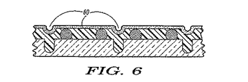
、前記ウエハは最終的には各個のフリップチップ12の端部または側面39を画定し得る溝38を伴ってその原型を保持し、分離していない状態である。図4を参照すると、アンダーフィル材40は工程24においてウエハ上にある各ICの活性表面36に適用される。前記アンダーフィル材は、被覆および半導体製造工程に共通である実に多くの方法によって適用され得る。例えば、アンダーフィル材溶液をウエハに被覆する方法として、浸漬、噴射、フラッドコート、スピンコート、またはカーテンコート等がある得る。或いは前記アンダーフィル材はステンシル、または印刷によって選択的に適用され得る。アンダーフィル材溶液の適用後、前記アンダーフィル材を少なくとも半固体状態にさせるように、例えば残留溶媒を除去するために加熱したり、前記アンダーフィル材が高固体材料である場合には、該材料を液体から固体へ変化させるために部分的に硬化させることによって、処理されなければならないことは明らかである。これまでに分かっている有用とされるアンダーフィル材には、エポキシ樹脂、ポリイミド樹脂、およびシリコンポリイミドコポリマー樹脂がある。前記アンダーフィル材が、溶液を浸漬、噴射、フラッドコート、スピンコート、またはカーテンコートすることによって、ウエハ表面上に大量に塗布されると、少なくとも部分的にはウエハ表面上に切断された溝を充填するであろう(42)。被膜42は、各ICの端部も同様に被覆する機能を有する。
Material with Fluxing Properties)」と題される米国特許番号第5128746号において説明されている。図5に示す別の実施形態において、前記アンダーフィル材がステンシル、印刷、または積層によって選択的に適用される場合、たとえアンダーフィル材が溝にあったとしても僅かであり、従って前記ICの端部39にもアンダーフィル材は残らない。
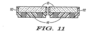
ル材が溝に堆積している場合、溝に残っているアンダーフィル材92を切断することによってダイ分離のための切断工程28が実行される。これはICの活性面または裏面から実行することができ、通常はレーザー(エキシマ、紫外線、二酸化炭素、またはその他のタイプ)を使用することによって、または機械的に切断またはソーイングすることによって達成される。ここで図11を参照すると、前記溝にあるアンダーフィル材92が切断された後に、個々のICチップ12は自由になり、各チップはダイシング工程22の間に画定された端部にアンダーフィル材112を有する。これは、二回目の切断のは通常、最初のダイシングによる切断よりも狭いためである。上記の両実施形態において、工程24において活性表面に堆積したアンダーフィル材40は、ウエハからダイ分離のための切断後もフリップチップIC112の活性表面に残る。
Claims (27)
- 集積回路チップにアンダーフィル材を提供し、前記チップをウエハからダイ分離するために切断する方法であって、以下に続く工程順によって、
a.前面および裏面を有するウエハを提供する工程と、前記ウエハは少なくとも一つの集積回路チップを含み、前記集積回路チップは前記ウエハの前面に複数のはんだバンプを有することと、
b.前記少なくとも一つの集積回路チップに端部を画定する溝を形成するために、前記ウエハの前面を切断する工程と、前記切断はウエハを完全に切断しない深さまでであることと、
c.前記ウエハの前面をアンダーフィル材で被覆する工程と、
d.前記ウエハの裏面を粗研磨して、前記溝が前面から裏面に及ぶまで十分に前記ウエハの厚さを減少させる工程とを備え、
e.前記前面上に被覆したアンダーフィル材は集積回路チップに付着した状態のまま残る方法。 - 工程(c)の後、前記複数のはんだバンプにフラックス剤による被覆を提供する工程を更に備える、請求項1記載の方法。
- 前記フラックス剤による被覆を提供する工程は、工程(c)の直後、および工程(d)の直前に行なわれる、請求項2記載の方法。
- 前記アンダーフィル材は、被覆する工程において、前記溝の内部、および前記集積回路チップの端部に堆積される、請求項1記載の方法。
- 前記粗研磨する工程は、前記ウエハの裏面を研削する、研磨する、または粗研磨する工程を備える、請求項1記載の方法。
- 前記被覆する工程は、液体材料を浸漬する、噴射する、または印刷する、または薄膜を積層する工程を備える、請求項1記載の方法。
- 前記集積回路はフリップチップ集積回路である、請求項1記載の方法。
- 前記アンダーフィル材は、エポキシ、ポリイミド、およびシリコンポリイミドコポリマーのうちから選択される、請求項1記載の方法。
- 前記被覆する工程(c)は、前記はんだバンプの各々を被覆する工程を更に備える、請求項1記載の方法。
- 前記被覆する工程(c)は、前記はんだバンプの各々の一部分を被覆せずに残す工程を備える、請求項1記載の方法。
- 集積回路チップにアンダーフィル材を提供するための方法であって、以下に続く工程順よって、
a.前面および裏面を有するウエハを提供する工程と、前記ウエハは少なくとも一つの集積回路チップを含み、前記集積回路チップは前記ウエハの前面に複数のはんだバンプを有することと、
b.前記少なくとも一つの集積回路チップに端部を画定する溝を形成するために、前記ウエハの前面を切断する工程と、前記切断はウエハを完全に切断しない深さまでであることと、
c.前記はんだバンプの各々の一部分を被覆せずに残すように、前記ウエハの前面をアンダーフィル材で被覆する工程と、
d.前記ウエハの裏面から材料を取り除いて、前記溝が前面から裏面に及ぶまで十分に前記ウエハの厚さを減少させる工程と、
e.前記ウエハから集積回路チップをダイ分離するために切断するのに十分であるように、溝にあるアンダーフィル材を切断することによってダイ分離する工程とを備える方法であって、
f.前記前面に被覆されたアンダーフィル材は、ダイ分離のために切断された集積回路チップに付着された状態のままに残る方法。 - 工程(c)の後、前記はんだバンプの被覆されていない部分にフラックス剤による被覆を提供する工程を更に備える、請求項11記載の方法。
- 前記フラックス剤による被覆を提供する工程は、前記アンダーフィル材にフラックス剤による被覆を提供する工程を更に備える、請求項12記載の方法。
- 前記フラックス剤による被覆を提供する工程は、工程(c)の直後、および工程(d)の直前に行なわれる、請求項12記載の方法。
- 前記アンダーフィル材は、被覆する工程において前記溝の内部、および前記集積回路チップの端部に堆積される、請求項11記載の方法。
- アンダーフィル材は、ダイ分離のための切断工程の後に前記集積回路チップの端部に被覆されたままに残る、請求項15記載の方法。
- 前記ダイ分離のための切断工程は、レーザー、スライシング、またはソーイングによってアンダーフィル材を切断する工程を備える、請求項11記載の方法。
- 前記ウエハの裏面から材料を取り除く工程は、ウエハの裏面を研削する、研磨する、または粗研磨する工程を備える、請求項11記載の方法。
- 前記被覆する工程は、液体材料を浸漬する、噴射する、または印刷する、または薄膜を積層する工程を備える、請求項11記載の方法。
- 前記集積回路はフリップチップ集積回路である、請求項11記載の方法。
- 前記アンダーフィル材は、エポキシ、ポリイミド、およびシリコンポリイミドコポリマーから構成される群から選択される、請求項11記載の方法。
- 前記切断工程はソーイング工程を備える、請求項11記載の方法。
- 導電性パッド上にはんだボールを備える活性表面を有する集積回路にアンダーフィル接着剤層を提供するためのウエハレベルの方法であって、
一つ以上の前記集積回路を含むシリコンウエハを提供する工程と、
前記集積回路の端部を画定する溝を形成するために、前記ウエハの活性表面を切断する工程と、前記切断はウエハを完全に切断しない深さまでであることと、
前記集積回路の活性表面上、および前記溝においてアンダーフィル接着剤層を形成する工程であって、ほとんどの前記はんだボールの内の少なくとも一部分は、アンダーフィル接着剤層に被覆されないままであることと、
前記アンダーフィル接着剤を部分的に硬化する工程と、
前記溝がウエハを完全に貫通するまで十分に前記ウエハの裏面からシリコンを除去する工程と、
前記溝に含まれるアンダーフィル接着剤を切断して、活性表面および端部にアンダーフィル材を有する集積回路を少なくとも一つダイ分離のために切断する工程とを備える方法。 - 前記はんだバンプの被覆されていない部分にフラックス剤による被覆を提供する工程を更に備える、請求項23記載の方法。
- 前記フラックス剤による被覆を提供する工程は、前記アンダーフィル材にフラックス剤による被覆を提供する工程を更に備える、請求項23記載の方法。
- 前記ウエハの裏面からシリコンを除去する工程は、前記ウエハの裏面を研削する、研磨する、または粗研磨する工程を備える、請求項23記載の方法。
- バンプを形成する集積回路の配列を有するウエハにアンダーフィル接着剤層を提供するための方法であって、各回路は導電性パッドにはんだボールを含む活性表面を有しており、
前記ウエハをダイシングして、ウエハの厚さよりも少ない所定の深さを有する溝を形成する工程と、
前記活性表面を被覆し、アンダーフィル材で溝を充填するように、前記ウエハをアンダーフィル材で被覆する工程と、
前記ダイシングされた溝が完全にウエハを貫通するまで、前記ウエハの活性表面の反対面を研磨する工程と、
前記溝にあるアンダーフィル材を通して切断し、前記バンプを形成する集積回路の配列をダイ分離するために切断する工程とを備える方法。
Applications Claiming Priority (2)
| Application Number | Priority Date | Filing Date | Title |
|---|---|---|---|
| US10/241,265 US6649445B1 (en) | 2002-09-11 | 2002-09-11 | Wafer coating and singulation method |
| PCT/US2003/027964 WO2004034422A2 (en) | 2002-09-11 | 2003-09-05 | Wafer coating and singulation method |
Publications (2)
| Publication Number | Publication Date |
|---|---|
| JP2005538572A true JP2005538572A (ja) | 2005-12-15 |
| JP2005538572A5 JP2005538572A5 (ja) | 2006-10-19 |
Family
ID=29420109
Family Applications (1)
| Application Number | Title | Priority Date | Filing Date |
|---|---|---|---|
| JP2004543275A Pending JP2005538572A (ja) | 2002-09-11 | 2003-09-05 | ウエハ被覆およびダイ分離するための切断方法 |
Country Status (6)
| Country | Link |
|---|---|
| US (1) | US6649445B1 (ja) |
| JP (1) | JP2005538572A (ja) |
| KR (1) | KR101054238B1 (ja) |
| CN (1) | CN100416768C (ja) |
| AU (1) | AU2003296904A1 (ja) |
| WO (1) | WO2004034422A2 (ja) |
Cited By (12)
| Publication number | Priority date | Publication date | Assignee | Title |
|---|---|---|---|---|
| JP2013021337A (ja) * | 2008-03-21 | 2013-01-31 | Hitachi Chem Co Ltd | 半導体装置の製造方法 |
| US8435868B2 (en) | 2009-01-20 | 2013-05-07 | Renesas Electronics Corporation | Semiconductor integrated circuit device and a method for manufacturing a semiconductor integrated circuit device |
| JP2016096279A (ja) * | 2014-11-17 | 2016-05-26 | インターナショナル・ビジネス・マシーンズ・コーポレーションInternational Business Machines Corporation | 回路モジュール及びその製造方法 |
| JP2017054888A (ja) * | 2015-09-08 | 2017-03-16 | 株式会社ディスコ | ウエーハの加工方法 |
| KR20170077029A (ko) * | 2015-12-25 | 2017-07-05 | 가부시기가이샤 디스코 | 웨이퍼의 가공 방법 |
| KR20190028317A (ko) * | 2017-09-08 | 2019-03-18 | 가부시기가이샤 디스코 | 웨이퍼의 가공 방법 |
| KR20190028315A (ko) * | 2017-09-08 | 2019-03-18 | 가부시기가이샤 디스코 | 웨이퍼의 가공 방법 |
| KR20190028301A (ko) * | 2017-09-08 | 2019-03-18 | 가부시기가이샤 디스코 | 웨이퍼의 가공 방법 |
| KR20190028316A (ko) * | 2017-09-08 | 2019-03-18 | 가부시기가이샤 디스코 | 웨이퍼의 가공 방법 |
| KR20190032191A (ko) * | 2017-09-19 | 2019-03-27 | 가부시기가이샤 디스코 | 웨이퍼의 가공 방법 |
| KR20190032192A (ko) * | 2017-09-19 | 2019-03-27 | 가부시기가이샤 디스코 | 웨이퍼의 가공 방법 |
| JP2019050264A (ja) * | 2017-09-08 | 2019-03-28 | 株式会社ディスコ | ウェーハの加工方法 |
Families Citing this family (62)
| Publication number | Priority date | Publication date | Assignee | Title |
|---|---|---|---|---|
| US6352881B1 (en) | 1999-07-22 | 2002-03-05 | National Semiconductor Corporation | Method and apparatus for forming an underfill adhesive layer |
| US6794751B2 (en) * | 2001-06-29 | 2004-09-21 | Intel Corporation | Multi-purpose planarizing/back-grind/pre-underfill arrangements for bumped wafers and dies |
| DE10202881B4 (de) * | 2002-01-25 | 2007-09-20 | Infineon Technologies Ag | Verfahren zur Herstellung von Halbleiterchips mit einer Chipkantenschutzschicht, insondere für Wafer Level Packaging Chips |
| US6908784B1 (en) * | 2002-03-06 | 2005-06-21 | Micron Technology, Inc. | Method for fabricating encapsulated semiconductor components |
| US7423337B1 (en) | 2002-08-19 | 2008-09-09 | National Semiconductor Corporation | Integrated circuit device package having a support coating for improved reliability during temperature cycling |
| US6903442B2 (en) | 2002-08-29 | 2005-06-07 | Micron Technology, Inc. | Semiconductor component having backside pin contacts |
| JP2004221125A (ja) * | 2003-01-09 | 2004-08-05 | Sharp Corp | 半導体装置及びその製造方法 |
| US7301222B1 (en) | 2003-02-12 | 2007-11-27 | National Semiconductor Corporation | Apparatus for forming a pre-applied underfill adhesive layer for semiconductor wafer level chip-scale packages |
| JP2004288816A (ja) * | 2003-03-20 | 2004-10-14 | Seiko Epson Corp | 半導体ウエハ、半導体装置及びその製造方法、回路基板並びに電子機器 |
| US20040235272A1 (en) * | 2003-05-23 | 2004-11-25 | Howard Gregory E. | Scribe street width reduction by deep trench and shallow saw cut |
| US6890836B2 (en) * | 2003-05-23 | 2005-05-10 | Texas Instruments Incorporated | Scribe street width reduction by deep trench and shallow saw cut |
| DE10333841B4 (de) * | 2003-07-24 | 2007-05-10 | Infineon Technologies Ag | Verfahren zur Herstellung eines Nutzens mit in Zeilen und Spalten angeordneten Halbleiterbauteilpositionen und Verfahren zur Herstellung eines Halbleiterbauteils |
| TWI231534B (en) * | 2003-12-11 | 2005-04-21 | Advanced Semiconductor Eng | Method for dicing a wafer |
| US7282375B1 (en) | 2004-04-14 | 2007-10-16 | National Semiconductor Corporation | Wafer level package design that facilitates trimming and testing |
| US7364945B2 (en) | 2005-03-31 | 2008-04-29 | Stats Chippac Ltd. | Method of mounting an integrated circuit package in an encapsulant cavity |
| US7354800B2 (en) | 2005-04-29 | 2008-04-08 | Stats Chippac Ltd. | Method of fabricating a stacked integrated circuit package system |
| KR100660868B1 (ko) * | 2005-07-06 | 2006-12-26 | 삼성전자주식회사 | 칩의 배면이 몰딩된 반도체 패키지 및 그의 제조방법 |
| US7273768B2 (en) * | 2005-08-30 | 2007-09-25 | Mutual-Pak Technology Co. Ltd. | Wafer-level package and IC module assembly method for the wafer-level package |
| US7768125B2 (en) * | 2006-01-04 | 2010-08-03 | Stats Chippac Ltd. | Multi-chip package system |
| US7456088B2 (en) | 2006-01-04 | 2008-11-25 | Stats Chippac Ltd. | Integrated circuit package system including stacked die |
| JP2007214268A (ja) * | 2006-02-08 | 2007-08-23 | Seiko Instruments Inc | 半導体装置の製造方法 |
| US7750482B2 (en) | 2006-02-09 | 2010-07-06 | Stats Chippac Ltd. | Integrated circuit package system including zero fillet resin |
| JP4791843B2 (ja) * | 2006-02-14 | 2011-10-12 | 株式会社ディスコ | 接着フィルム付きデバイスの製造方法 |
| US8704349B2 (en) | 2006-02-14 | 2014-04-22 | Stats Chippac Ltd. | Integrated circuit package system with exposed interconnects |
| US7385299B2 (en) * | 2006-02-25 | 2008-06-10 | Stats Chippac Ltd. | Stackable integrated circuit package system with multiple interconnect interface |
| JP5275553B2 (ja) * | 2006-06-27 | 2013-08-28 | スリーエム イノベイティブ プロパティズ カンパニー | 分割チップの製造方法 |
| US7482251B1 (en) * | 2006-08-10 | 2009-01-27 | Impinj, Inc. | Etch before grind for semiconductor die singulation |
| US9111950B2 (en) | 2006-09-28 | 2015-08-18 | Philips Lumileds Lighting Company, Llc | Process for preparing a semiconductor structure for mounting |
| JP5091600B2 (ja) | 2006-09-29 | 2012-12-05 | 三洋電機株式会社 | 半導体モジュール、半導体モジュールの製造方法および携帯機器 |
| JP4933233B2 (ja) | 2006-11-30 | 2012-05-16 | 株式会社ディスコ | ウエーハの加工方法 |
| JP4345808B2 (ja) * | 2006-12-15 | 2009-10-14 | エルピーダメモリ株式会社 | 半導体装置の製造方法 |
| KR100842505B1 (ko) * | 2006-12-19 | 2008-07-01 | 동부일렉트로닉스 주식회사 | 웨이퍼 백면의 메탈 증착공정 |
| TWI364793B (en) * | 2007-05-08 | 2012-05-21 | Mutual Pak Technology Co Ltd | Package structure for integrated circuit device and method of the same |
| US7727875B2 (en) * | 2007-06-21 | 2010-06-01 | Stats Chippac, Ltd. | Grooving bumped wafer pre-underfill system |
| US7838424B2 (en) * | 2007-07-03 | 2010-11-23 | Taiwan Semiconductor Manufacturing Company, Ltd. | Enhanced reliability of wafer-level chip-scale packaging (WLCSP) die separation using dry etching |
| US20090155981A1 (en) * | 2007-12-13 | 2009-06-18 | Ayotte Stephen P | Method and apparatus for singulating integrated circuit chips |
| US7824962B2 (en) * | 2008-01-29 | 2010-11-02 | Infineon Technologies Ag | Method of integrated circuit fabrication |
| CN101521164B (zh) * | 2008-02-26 | 2011-01-05 | 上海凯虹科技电子有限公司 | 引线键合芯片级封装方法 |
| US8058150B2 (en) * | 2008-07-10 | 2011-11-15 | Taiwan Semiconductor Manufacturing Company, Ltd. | Particle free wafer separation |
| US7989950B2 (en) * | 2008-08-14 | 2011-08-02 | Stats Chippac Ltd. | Integrated circuit packaging system having a cavity |
| US7776649B1 (en) * | 2009-05-01 | 2010-08-17 | Powertech Technology Inc. | Method for fabricating wafer level chip scale packages |
| CN101941181B (zh) * | 2009-07-03 | 2012-10-17 | 日月光半导体制造股份有限公司 | 晶圆的研磨方法 |
| CN102237307A (zh) * | 2010-04-27 | 2011-11-09 | 瑞鼎科技股份有限公司 | 集成电路晶圆切割方法 |
| US9224647B2 (en) | 2010-09-24 | 2015-12-29 | Stats Chippac, Ltd. | Semiconductor device and method of forming TSV interposer with semiconductor die and build-up interconnect structure on opposing surfaces of the interposer |
| US8993377B2 (en) | 2010-09-29 | 2015-03-31 | Stats Chippac, Ltd. | Semiconductor device and method of bonding different size semiconductor die at the wafer level |
| US8652935B2 (en) | 2010-12-16 | 2014-02-18 | Tessera, Inc. | Void-free wafer bonding using channels |
| US20120273935A1 (en) * | 2011-04-29 | 2012-11-01 | Stefan Martens | Semiconductor Device and Method of Making a Semiconductor Device |
| JP5888995B2 (ja) | 2012-01-16 | 2016-03-22 | 三菱電機株式会社 | 半導体装置およびその製造方法 |
| US8940618B2 (en) * | 2012-03-13 | 2015-01-27 | Taiwan Semiconductor Manufacturing Company, Ltd. | Method and device for cutting semiconductor wafers |
| CN102825541B (zh) * | 2012-09-10 | 2014-12-10 | 豪威科技(上海)有限公司 | 晶圆减薄方法 |
| US9631065B2 (en) * | 2013-03-12 | 2017-04-25 | Intel Corporation | Methods of forming wafer level underfill materials and structures formed thereby |
| US9508623B2 (en) | 2014-06-08 | 2016-11-29 | UTAC Headquarters Pte. Ltd. | Semiconductor packages and methods of packaging semiconductor devices |
| US9704823B2 (en) * | 2015-03-21 | 2017-07-11 | Nxp B.V. | Reduction of defects in wafer level chip scale package (WLCSP) devices |
| US11037904B2 (en) | 2015-11-24 | 2021-06-15 | Taiwan Semiconductor Manufacturing Company, Ltd. | Singulation and bonding methods and structures formed thereby |
| JP6523999B2 (ja) * | 2016-03-14 | 2019-06-05 | 東芝メモリ株式会社 | 半導体装置およびその製造方法 |
| JP6767814B2 (ja) * | 2016-09-05 | 2020-10-14 | 株式会社ディスコ | パッケージデバイスチップの製造方法 |
| JP6746224B2 (ja) * | 2016-11-18 | 2020-08-26 | 株式会社ディスコ | デバイスチップパッケージの製造方法 |
| US10529671B2 (en) * | 2016-12-13 | 2020-01-07 | Taiwan Semiconductor Manufacturing Co., Ltd. | Package structure and method for forming the same |
| US10510709B2 (en) * | 2017-04-20 | 2019-12-17 | Taiwan Semiconductor Manufacturing Co., Ltd. | Semicondcutor package and manufacturing method thereof |
| CN109102772B (zh) * | 2017-06-20 | 2023-11-21 | 昆山国显光电有限公司 | 驱动电路板和显示装置 |
| KR102506698B1 (ko) * | 2018-02-19 | 2023-03-07 | 에스케이하이닉스 주식회사 | 보강용 탑 다이를 포함하는 반도체 패키지 제조 방법 |
| US11908831B2 (en) | 2020-10-21 | 2024-02-20 | Stmicroelectronics Pte Ltd | Method for manufacturing a wafer level chip scale package (WLCSP) |
Citations (10)
| Publication number | Priority date | Publication date | Assignee | Title |
|---|---|---|---|---|
| JPH1079362A (ja) * | 1996-07-12 | 1998-03-24 | Fujitsu Ltd | 半導体装置の製造方法及び半導体装置製造用金型及び半導体装置及びその実装方法 |
| JPH11111646A (ja) * | 1997-10-02 | 1999-04-23 | Fujitsu Ltd | 半導体装置の製造方法及び半導体装置 |
| JP2000208559A (ja) * | 1999-01-12 | 2000-07-28 | Oki Electric Ind Co Ltd | 樹脂封止型半導体装置及びその製造方法 |
| JP2000294519A (ja) * | 1999-04-09 | 2000-10-20 | Oki Electric Ind Co Ltd | 半導体装置、半導体装置の製造方法、およびその実装方法 |
| JP2001127206A (ja) * | 1999-08-13 | 2001-05-11 | Citizen Watch Co Ltd | チップスケールパッケージの製造方法及びicチップの製造方法 |
| JP2001332520A (ja) * | 2000-05-23 | 2001-11-30 | Amkor Technology Inc | シート状樹脂組成物及びそれを用いた半導体装置の製造方法 |
| JP2002016022A (ja) * | 2000-06-29 | 2002-01-18 | Toshiba Corp | 半導体装置の製造方法 |
| JP2002100709A (ja) * | 2000-09-21 | 2002-04-05 | Hitachi Ltd | 半導体装置及びその製造方法 |
| JP2002513208A (ja) * | 1998-04-27 | 2002-05-08 | アルファ・メタルズ・インコーポレーテッド | 一体化したフラックス、マスク及びアンダーフィルを備えるフリップフロップ |
| JP2003017513A (ja) * | 2001-07-04 | 2003-01-17 | Toshiba Corp | 半導体装置の製造方法 |
Family Cites Families (14)
| Publication number | Priority date | Publication date | Assignee | Title |
|---|---|---|---|---|
| US5128746A (en) | 1990-09-27 | 1992-07-07 | Motorola, Inc. | Adhesive and encapsulant material with fluxing properties |
| JP3376203B2 (ja) | 1996-02-28 | 2003-02-10 | 株式会社東芝 | 半導体装置とその製造方法及びこの半導体装置を用いた実装構造体とその製造方法 |
| AU8502798A (en) | 1997-07-21 | 1999-02-10 | Aguila Technologies, Inc. | Semiconductor flip-chip package and method for the fabrication thereof |
| US6184109B1 (en) * | 1997-07-23 | 2001-02-06 | Kabushiki Kaisha Toshiba | Method of dividing a wafer and method of manufacturing a semiconductor device |
| US6323062B1 (en) | 1998-04-27 | 2001-11-27 | Alpha Metals, Inc. | Wafer coating method for flip chips |
| JP3516592B2 (ja) * | 1998-08-18 | 2004-04-05 | 沖電気工業株式会社 | 半導体装置およびその製造方法 |
| US6168972B1 (en) | 1998-12-22 | 2001-01-02 | Fujitsu Limited | Flip chip pre-assembly underfill process |
| US6194788B1 (en) | 1999-03-10 | 2001-02-27 | Alpha Metals, Inc. | Flip chip with integrated flux and underfill |
| US6352881B1 (en) * | 1999-07-22 | 2002-03-05 | National Semiconductor Corporation | Method and apparatus for forming an underfill adhesive layer |
| JP3455762B2 (ja) * | 1999-11-11 | 2003-10-14 | カシオ計算機株式会社 | 半導体装置およびその製造方法 |
| US6524890B2 (en) * | 1999-11-17 | 2003-02-25 | Denso Corporation | Method for manufacturing semiconductor device having element isolation structure |
| JP2001176899A (ja) * | 1999-12-21 | 2001-06-29 | Sanyo Electric Co Ltd | 半導体装置の製造方法 |
| US6528393B2 (en) * | 2000-06-13 | 2003-03-04 | Advanced Semiconductor Engineering, Inc. | Method of making a semiconductor package by dicing a wafer from the backside surface thereof |
| US6506681B2 (en) | 2000-12-06 | 2003-01-14 | Micron Technology, Inc. | Thin flip—chip method |
-
2002
- 2002-09-11 US US10/241,265 patent/US6649445B1/en not_active Expired - Lifetime
-
2003
- 2003-09-05 AU AU2003296904A patent/AU2003296904A1/en not_active Abandoned
- 2003-09-05 JP JP2004543275A patent/JP2005538572A/ja active Pending
- 2003-09-05 KR KR1020057004220A patent/KR101054238B1/ko not_active IP Right Cessation
- 2003-09-05 CN CNB038214520A patent/CN100416768C/zh not_active Expired - Fee Related
- 2003-09-05 WO PCT/US2003/027964 patent/WO2004034422A2/en active Application Filing
Patent Citations (10)
| Publication number | Priority date | Publication date | Assignee | Title |
|---|---|---|---|---|
| JPH1079362A (ja) * | 1996-07-12 | 1998-03-24 | Fujitsu Ltd | 半導体装置の製造方法及び半導体装置製造用金型及び半導体装置及びその実装方法 |
| JPH11111646A (ja) * | 1997-10-02 | 1999-04-23 | Fujitsu Ltd | 半導体装置の製造方法及び半導体装置 |
| JP2002513208A (ja) * | 1998-04-27 | 2002-05-08 | アルファ・メタルズ・インコーポレーテッド | 一体化したフラックス、マスク及びアンダーフィルを備えるフリップフロップ |
| JP2000208559A (ja) * | 1999-01-12 | 2000-07-28 | Oki Electric Ind Co Ltd | 樹脂封止型半導体装置及びその製造方法 |
| JP2000294519A (ja) * | 1999-04-09 | 2000-10-20 | Oki Electric Ind Co Ltd | 半導体装置、半導体装置の製造方法、およびその実装方法 |
| JP2001127206A (ja) * | 1999-08-13 | 2001-05-11 | Citizen Watch Co Ltd | チップスケールパッケージの製造方法及びicチップの製造方法 |
| JP2001332520A (ja) * | 2000-05-23 | 2001-11-30 | Amkor Technology Inc | シート状樹脂組成物及びそれを用いた半導体装置の製造方法 |
| JP2002016022A (ja) * | 2000-06-29 | 2002-01-18 | Toshiba Corp | 半導体装置の製造方法 |
| JP2002100709A (ja) * | 2000-09-21 | 2002-04-05 | Hitachi Ltd | 半導体装置及びその製造方法 |
| JP2003017513A (ja) * | 2001-07-04 | 2003-01-17 | Toshiba Corp | 半導体装置の製造方法 |
Cited By (26)
| Publication number | Priority date | Publication date | Assignee | Title |
|---|---|---|---|---|
| JP2013021337A (ja) * | 2008-03-21 | 2013-01-31 | Hitachi Chem Co Ltd | 半導体装置の製造方法 |
| US8435868B2 (en) | 2009-01-20 | 2013-05-07 | Renesas Electronics Corporation | Semiconductor integrated circuit device and a method for manufacturing a semiconductor integrated circuit device |
| US10679916B2 (en) | 2014-11-17 | 2020-06-09 | International Business Machines Corporation | Circuit module and manufacturing method thereof |
| JP2016096279A (ja) * | 2014-11-17 | 2016-05-26 | インターナショナル・ビジネス・マシーンズ・コーポレーションInternational Business Machines Corporation | 回路モジュール及びその製造方法 |
| US10074583B2 (en) | 2014-11-17 | 2018-09-11 | International Business Machines Corporation | Circuit module and manufacturing method thereof |
| JP2017054888A (ja) * | 2015-09-08 | 2017-03-16 | 株式会社ディスコ | ウエーハの加工方法 |
| KR20170077029A (ko) * | 2015-12-25 | 2017-07-05 | 가부시기가이샤 디스코 | 웨이퍼의 가공 방법 |
| KR102505700B1 (ko) * | 2015-12-25 | 2023-03-02 | 가부시기가이샤 디스코 | 웨이퍼의 가공 방법 |
| KR20190028317A (ko) * | 2017-09-08 | 2019-03-18 | 가부시기가이샤 디스코 | 웨이퍼의 가공 방법 |
| TWI788410B (zh) * | 2017-09-08 | 2023-01-01 | 日商迪思科股份有限公司 | 晶圓之加工方法 |
| CN109494189A (zh) * | 2017-09-08 | 2019-03-19 | 株式会社迪思科 | 晶片的加工方法 |
| KR102627958B1 (ko) * | 2017-09-08 | 2024-01-19 | 가부시기가이샤 디스코 | 웨이퍼의 가공 방법 |
| CN109494189B (zh) * | 2017-09-08 | 2023-10-13 | 株式会社迪思科 | 晶片的加工方法 |
| JP2019050264A (ja) * | 2017-09-08 | 2019-03-28 | 株式会社ディスコ | ウェーハの加工方法 |
| JP2019050248A (ja) * | 2017-09-08 | 2019-03-28 | 株式会社ディスコ | ウェーハの加工方法 |
| KR20190028301A (ko) * | 2017-09-08 | 2019-03-18 | 가부시기가이샤 디스코 | 웨이퍼의 가공 방법 |
| JP7058904B2 (ja) | 2017-09-08 | 2022-04-25 | 株式会社ディスコ | ウェーハの加工方法 |
| KR20190028316A (ko) * | 2017-09-08 | 2019-03-18 | 가부시기가이샤 디스코 | 웨이퍼의 가공 방법 |
| KR20190028315A (ko) * | 2017-09-08 | 2019-03-18 | 가부시기가이샤 디스코 | 웨이퍼의 가공 방법 |
| KR102581131B1 (ko) * | 2017-09-08 | 2023-09-20 | 가부시기가이샤 디스코 | 웨이퍼의 가공 방법 |
| KR102581132B1 (ko) * | 2017-09-08 | 2023-09-20 | 가부시기가이샤 디스코 | 웨이퍼의 가공 방법 |
| KR102581138B1 (ko) * | 2017-09-08 | 2023-09-20 | 가부시기가이샤 디스코 | 웨이퍼의 가공 방법 |
| KR102569622B1 (ko) * | 2017-09-19 | 2023-08-22 | 가부시기가이샤 디스코 | 웨이퍼의 가공 방법 |
| KR102569623B1 (ko) * | 2017-09-19 | 2023-08-22 | 가부시기가이샤 디스코 | 웨이퍼의 가공 방법 |
| KR20190032192A (ko) * | 2017-09-19 | 2019-03-27 | 가부시기가이샤 디스코 | 웨이퍼의 가공 방법 |
| KR20190032191A (ko) * | 2017-09-19 | 2019-03-27 | 가부시기가이샤 디스코 | 웨이퍼의 가공 방법 |
Also Published As
| Publication number | Publication date |
|---|---|
| CN100416768C (zh) | 2008-09-03 |
| AU2003296904A1 (en) | 2004-05-04 |
| AU2003296904A8 (en) | 2004-05-04 |
| WO2004034422A3 (en) | 2004-08-26 |
| KR20050054933A (ko) | 2005-06-10 |
| CN1682363A (zh) | 2005-10-12 |
| KR101054238B1 (ko) | 2011-08-08 |
| WO2004034422A2 (en) | 2004-04-22 |
| US6649445B1 (en) | 2003-11-18 |
Similar Documents
| Publication | Publication Date | Title |
|---|---|---|
| JP2005538572A (ja) | ウエハ被覆およびダイ分離するための切断方法 | |
| US8030769B2 (en) | Grooving bumped wafer pre-underfill system | |
| US6251705B1 (en) | Low profile integrated circuit packages | |
| US6924171B2 (en) | Bilayer wafer-level underfill | |
| US8501543B1 (en) | Direct-write wafer level chip scale package | |
| CN102024802B (zh) | 集成电路结构及其形成方法 | |
| US8741762B2 (en) | Through silicon via dies and packages | |
| US6710454B1 (en) | Adhesive layer for an electronic apparatus having multiple semiconductor devices | |
| US7064010B2 (en) | Methods of coating and singulating wafers | |
| KR100247463B1 (ko) | 탄성중합체를 포함하는 반도체 집적회로 소자의 제조 방법 | |
| US7445963B2 (en) | Semiconductor package having an interfacial adhesive layer | |
| JP4497112B2 (ja) | 半導体装置の製造方法 | |
| US20020167085A1 (en) | Semiconductor device and method of fabricating the same | |
| US20030143819A1 (en) | Method of producing semiconductor chips with a chip edge guard, in particular for wafer level packaging chips | |
| JP2000068401A (ja) | 半導体装置およびその製造方法 | |
| JP2006196701A (ja) | 半導体装置の製造方法 | |
| US6083773A (en) | Methods of forming flip chip bumps and related flip chip bump constructions | |
| US6916684B2 (en) | Wafer-applied underfill process | |
| US20040053445A1 (en) | Method of assembling a package with an exposed die backside with and without a heatsink for flip-chip | |
| JP2008130704A (ja) | 半導体装置の製造方法 | |
| JPH1154556A (ja) | 半導体装置とその製造方法 | |
| JP2004525512A (ja) | フリップチップの相互接続を精度良く封止するための装置及び方法 | |
| US6207478B1 (en) | Method for manufacturing semiconductor package of center pad type device | |
| US20210335628A1 (en) | Flip-chip package with reduced underfill area | |
| JP4778667B2 (ja) | アンダーフィル用シート材、半導体チップのアンダーフィル方法および半導体チップの実装方法 |
Legal Events
| Date | Code | Title | Description |
|---|---|---|---|
| A521 | Written amendment |
Free format text: JAPANESE INTERMEDIATE CODE: A523 Effective date: 20060904 |
|
| A621 | Written request for application examination |
Free format text: JAPANESE INTERMEDIATE CODE: A621 Effective date: 20060904 |
|
| A131 | Notification of reasons for refusal |
Free format text: JAPANESE INTERMEDIATE CODE: A131 Effective date: 20090616 |
|
| A601 | Written request for extension of time |
Free format text: JAPANESE INTERMEDIATE CODE: A601 Effective date: 20090916 |
|
| A602 | Written permission of extension of time |
Free format text: JAPANESE INTERMEDIATE CODE: A602 Effective date: 20090928 |
|
| A601 | Written request for extension of time |
Free format text: JAPANESE INTERMEDIATE CODE: A601 Effective date: 20091016 |
|
| A602 | Written permission of extension of time |
Free format text: JAPANESE INTERMEDIATE CODE: A602 Effective date: 20091023 |
|
| A521 | Written amendment |
Free format text: JAPANESE INTERMEDIATE CODE: A523 Effective date: 20091030 |
|
| A131 | Notification of reasons for refusal |
Free format text: JAPANESE INTERMEDIATE CODE: A131 Effective date: 20091201 |
|
| A521 | Written amendment |
Free format text: JAPANESE INTERMEDIATE CODE: A523 Effective date: 20100219 |
|
| A02 | Decision of refusal |
Free format text: JAPANESE INTERMEDIATE CODE: A02 Effective date: 20100323 |