JP2005513774A - Nチャネルトランジスタおよびpチャネルトランジスタのそれぞれを最適化する、異なるスペーサを形成する方法 - Google Patents
Nチャネルトランジスタおよびpチャネルトランジスタのそれぞれを最適化する、異なるスペーサを形成する方法 Download PDFInfo
- Publication number
- JP2005513774A JP2005513774A JP2003553602A JP2003553602A JP2005513774A JP 2005513774 A JP2005513774 A JP 2005513774A JP 2003553602 A JP2003553602 A JP 2003553602A JP 2003553602 A JP2003553602 A JP 2003553602A JP 2005513774 A JP2005513774 A JP 2005513774A
- Authority
- JP
- Japan
- Prior art keywords
- channel transistor
- spacer
- source
- offset spacer
- forming
- Prior art date
- Legal status (The legal status is an assumption and is not a legal conclusion. Google has not performed a legal analysis and makes no representation as to the accuracy of the status listed.)
- Pending
Links
Images


Classifications
-
- H—ELECTRICITY
- H01—ELECTRIC ELEMENTS
- H01L—SEMICONDUCTOR DEVICES NOT COVERED BY CLASS H10
- H01L21/00—Processes or apparatus adapted for the manufacture or treatment of semiconductor or solid state devices or of parts thereof
- H01L21/70—Manufacture or treatment of devices consisting of a plurality of solid state components formed in or on a common substrate or of parts thereof; Manufacture of integrated circuit devices or of parts thereof
- H01L21/77—Manufacture or treatment of devices consisting of a plurality of solid state components or integrated circuits formed in, or on, a common substrate
- H01L21/78—Manufacture or treatment of devices consisting of a plurality of solid state components or integrated circuits formed in, or on, a common substrate with subsequent division of the substrate into plural individual devices
- H01L21/82—Manufacture or treatment of devices consisting of a plurality of solid state components or integrated circuits formed in, or on, a common substrate with subsequent division of the substrate into plural individual devices to produce devices, e.g. integrated circuits, each consisting of a plurality of components
- H01L21/822—Manufacture or treatment of devices consisting of a plurality of solid state components or integrated circuits formed in, or on, a common substrate with subsequent division of the substrate into plural individual devices to produce devices, e.g. integrated circuits, each consisting of a plurality of components the substrate being a semiconductor, using silicon technology
- H01L21/8232—Field-effect technology
- H01L21/8234—MIS technology, i.e. integration processes of field effect transistors of the conductor-insulator-semiconductor type
- H01L21/8238—Complementary field-effect transistors, e.g. CMOS
- H01L21/823814—Complementary field-effect transistors, e.g. CMOS with a particular manufacturing method of the source or drain structures, e.g. specific source or drain implants or silicided source or drain structures or raised source or drain structures
-
- H—ELECTRICITY
- H01—ELECTRIC ELEMENTS
- H01L—SEMICONDUCTOR DEVICES NOT COVERED BY CLASS H10
- H01L21/00—Processes or apparatus adapted for the manufacture or treatment of semiconductor or solid state devices or of parts thereof
- H01L21/70—Manufacture or treatment of devices consisting of a plurality of solid state components formed in or on a common substrate or of parts thereof; Manufacture of integrated circuit devices or of parts thereof
- H01L21/77—Manufacture or treatment of devices consisting of a plurality of solid state components or integrated circuits formed in, or on, a common substrate
- H01L21/78—Manufacture or treatment of devices consisting of a plurality of solid state components or integrated circuits formed in, or on, a common substrate with subsequent division of the substrate into plural individual devices
- H01L21/82—Manufacture or treatment of devices consisting of a plurality of solid state components or integrated circuits formed in, or on, a common substrate with subsequent division of the substrate into plural individual devices to produce devices, e.g. integrated circuits, each consisting of a plurality of components
- H01L21/822—Manufacture or treatment of devices consisting of a plurality of solid state components or integrated circuits formed in, or on, a common substrate with subsequent division of the substrate into plural individual devices to produce devices, e.g. integrated circuits, each consisting of a plurality of components the substrate being a semiconductor, using silicon technology
- H01L21/8232—Field-effect technology
- H01L21/8234—MIS technology, i.e. integration processes of field effect transistors of the conductor-insulator-semiconductor type
- H01L21/8238—Complementary field-effect transistors, e.g. CMOS
- H01L21/823864—Complementary field-effect transistors, e.g. CMOS with a particular manufacturing method of the gate sidewall spacers, e.g. double spacers, particular spacer material or shape
-
- H—ELECTRICITY
- H01—ELECTRIC ELEMENTS
- H01L—SEMICONDUCTOR DEVICES NOT COVERED BY CLASS H10
- H01L27/00—Devices consisting of a plurality of semiconductor or other solid-state components formed in or on a common substrate
- H01L27/02—Devices consisting of a plurality of semiconductor or other solid-state components formed in or on a common substrate including semiconductor components specially adapted for rectifying, oscillating, amplifying or switching and having at least one potential-jump barrier or surface barrier; including integrated passive circuit elements with at least one potential-jump barrier or surface barrier
- H01L27/04—Devices consisting of a plurality of semiconductor or other solid-state components formed in or on a common substrate including semiconductor components specially adapted for rectifying, oscillating, amplifying or switching and having at least one potential-jump barrier or surface barrier; including integrated passive circuit elements with at least one potential-jump barrier or surface barrier the substrate being a semiconductor body
- H01L27/08—Devices consisting of a plurality of semiconductor or other solid-state components formed in or on a common substrate including semiconductor components specially adapted for rectifying, oscillating, amplifying or switching and having at least one potential-jump barrier or surface barrier; including integrated passive circuit elements with at least one potential-jump barrier or surface barrier the substrate being a semiconductor body including only semiconductor components of a single kind
- H01L27/085—Devices consisting of a plurality of semiconductor or other solid-state components formed in or on a common substrate including semiconductor components specially adapted for rectifying, oscillating, amplifying or switching and having at least one potential-jump barrier or surface barrier; including integrated passive circuit elements with at least one potential-jump barrier or surface barrier the substrate being a semiconductor body including only semiconductor components of a single kind including field-effect components only
- H01L27/088—Devices consisting of a plurality of semiconductor or other solid-state components formed in or on a common substrate including semiconductor components specially adapted for rectifying, oscillating, amplifying or switching and having at least one potential-jump barrier or surface barrier; including integrated passive circuit elements with at least one potential-jump barrier or surface barrier the substrate being a semiconductor body including only semiconductor components of a single kind including field-effect components only the components being field-effect transistors with insulated gate
- H01L27/092—Devices consisting of a plurality of semiconductor or other solid-state components formed in or on a common substrate including semiconductor components specially adapted for rectifying, oscillating, amplifying or switching and having at least one potential-jump barrier or surface barrier; including integrated passive circuit elements with at least one potential-jump barrier or surface barrier the substrate being a semiconductor body including only semiconductor components of a single kind including field-effect components only the components being field-effect transistors with insulated gate complementary MIS field-effect transistors
Abstract
Description
超々大規模集積回路(ULSI)半導体デバイスに関連する高密度化および高性能に対する要求が高まっており、構造的要素の縮小、トランジスタ速度と回路速度の高速化、高い信頼性、および生産スループットを増加して、競争力を高めることが必要とされている。
デバイスおよび構造が縮小されるにつれて、また、より高性能なデバイスへの要求が高めるにつれて、新たな製造方法または新たな配置を必要とする、新たな問題が発見される。
MOSデバイスは典型的に、半導体基板中にイオン注入される一対のソース/ドレイン領域と、このソース/ドレイン領域を分離するチャネル領域とを含む。
典型的にチャネル領域の上には、薄いゲート酸化膜および伝導性のポリシリコンまたは他の導電材料を含んだ伝導性のゲートがある。
典型的な集積回路は、n型およびp型のような異なる導電型の複数のMOSデバイスと、共通基板上で形成されるpチャネルおよびnチャネルデバイスの両方を使用するCMOS(complementary MOS)デバイスとを有する。
CMOS技術は、信頼性、回路性能およびコスト利点と同様に、出力密度および損失(dissipation)の著しい低減という利点を有する。
小型デバイスは、単一のチップ上に、より機能回路を搭載するため、利用可能な領域を容易に増やすことができる。
小型デバイスはまた、スイッチング時間がより短い点から本質的に有利である。
デバイスの寄生キャパシタンスに関連する1つの要素は「ミラー・キャパシタンス」とも呼ばれるゲート・ドレイン間のオーバーラップ・キャパシタンスである。
このゲート・ドレイン間のオーバーラップ・キャパシタンスは、デバイスのスイッチング時間に重要な影響を与える。
低いチャネル抵抗を維持するが、さらにゲート・ドレイン間のオーバーラップ・キャパシタンスを最小限にするように、ソース/ドレインの十分なゲート・オーバーラップを得ることは重要である。
使用されている方法の一つは、ソース/ドレイン拡張部の注入ステップの間、ゲート電極上のオフセットスペーサを使用することを含んでいる。
オフセットスペーサは、このスペーサの真下にある基板中へのドーパントの注入を防止するためのマスクの役割を果たす。このように、ソース/ドレイン拡張部とゲート電極間の分離距離(separation)が増加する。
これは、nチャネルトランジスタとpチャネルトランジスタの両方を含む半導体デバイス中において問題を生成する。
オーバーラップ・キャパシタンスを最小限にするオフセットスペーサの形成は、一方の型のトランジスタ(例えば、nチャネル)を最適化し、他方の型(例えば、pチャネル)を最適化しない。
換言すると、nチャネルトランジスタについてのゲート・ドレイン間のオーバーラップ・キャパシタンスを最適化する最適な幅を有するオフセットスペーサの提供は、シリコン中のホウ素の拡散がより速いことにより、pチャネルトランジスタを最適化するような最適なスペーシングを提供することにはならない。
ソース/ドレイン拡張部は、p型のドーパントを第2ゲート電極から第2間隔を隔てて注入することによって、pチャネルトランジスタ中で形成される。この第2間隔は、第1間隔よりも大きい。
本発明のある実施形態においては、n型ドーパントは第1スペーサ幅に従って注入され、p型ドーパントは第2スペーサ幅に従って注入される。
本発明のある実施形態においては、この第1スペーサ幅は、nチャネルトランジスタおよびpチャネルトランジスタのゲート電極上の第1オフセットスペーサの幅と等しい。
第2スペーサ幅は、対となるオフセットスペーサを形成すべく、第1オフセットスペーサ上に形成される第1オフセットスペーサと第2オフセットスペーサの合計幅と等しい。
この方法は、nチャネルトランジスタおよびpチャネルトランジスタのゲート電極上に第1オフセットスペーサを形成するステップを含む。
ソース/ドレイン拡張部は、第1オフセットスペーサの真下の基板への注入をマスクする第1オフセットスペーサ(18)を使用すると共に、nチャネルトランジスタの基板中のみに注入される。
第2オフセットスペーサは、第1オフセットスペーサ上に形成される。
その後ソース/ドレイン拡張部は、pチャネルトランジスタの基板中のみに注入される。第1オフセットスペーサおよび第2オフセットスペーサは、第1オフセットスペーサおよび第2オフセットスペーサの真下の基板への注入をマスクする。
本発明は、ゲート電極からの異なる(differencial)スペーシングでソース/ドレイン拡張部のドーパントを注入することによって、nチャネルトランジスタとpチャネルトランジスタのそれぞれのオーバーラップ・キャパシタンスを最適化する。
これは、ゲート電極上に第1オフセットスペーサを形成し、nチャネルトランジスタ中のみにソース/ドレイン拡張部のインプラントを生成することによって遂行される。
第2オフセットスペーサは、この第1オフセットスペーサ上に形成され、pチャネルトランジスタ中にソース/ドレイン拡張部のインプラントが生成される。
従って、pチャネルトランジスタ中のソース/ドレイン拡張部のインプラントは、nチャネルトランジスタ中のソース/ドレイン拡張部よりゲート電極からの間隔がさらにあけられる。これは、ホウ素のようなp型のドーパントの拡散が、より速いためである。
これは、nチャネルトランジスタおよびpチャネルトランジスタの双方のオーバーラップ・キャパシタンスを最適化することを可能にする。
特に言及される場合を除き、以下の記載では、層を形成し、エッチングし、そして基板にドーパントを注入するための従来の処理方法を使用するものとする。
図1に示すように、基板10は、nチャネルトランジスタおよびpチャネルトランジスタ用の共通基板を形成する。
nチャネルトランジスタ12は、ゲート電極16を有しており、pチャネルトランジスタ14もゲート電極16を有している。
ゲート電極16は、基板10上にポリシリコン・ゲート層をたい積することによるような従来の方式、従来のフォトリソグラフィ技術およびエッチング技術で形成される。
第1オフセットスペーサ18は、例えば窒化シリコンまたは酸化シリコンのような、従来のスペーサ材料から構成されていてもよいが、例えばシリコン酸窒化物(silicon oxynitride)のような、他の材料が使用されてもよい。
第1オフセットスペーサのたい積および形成は、全基板10およびゲート電極16上の第1スペーサ層(図示しない)中に第1スペーサ材料をたい積することを含む。
nチャネルトランジスタのゲート・ドレイン間のオーバーラップ・キャパシタンスを最適化すべく、エッチング後に第1オフセットスペーサ18が所望の幅を有するように、第1スペーサ層の厚みを選択してもよい。
例えば、第1スペーサ層の深さは、約100Åから約300Åの間とすることができる。
反応性イオンエッチングのような従来の異方性エッチングの後、第1オフセットスペーサ18は、基板10上に約60Åから約180Åの間の幅を有するようにして形成される。
このスペーシングは通常、最適なゲート・ドレイン間のオーバーラップキャパシタンスを提供するため、nチャネルトランジスタのオフセットスペーサに適切であると考えられる。
この例から理解できるように、この異方性エッチングは、スペーサ層の厚みのおよそ60%の幅を有するスペーサ18を生産する。
より厚いまたはより薄いスペーサ層の厚み、またはエッチング技術における変形例においては、所望のオーバーラップ・キャパシタンスを生産するように調整されたオフセットスペーサの幅を生産することができる。
pチャネルトランジスタ14は、この注入プロセスの間、pチャネルトランジスタ14をn型ドーパントの注入から保護すべく、マスクされる。
イオン注入は、例えばヒ素のようなn型ドーパントを基板10中に注入するように実行することができる。
注入されたドーパントは、nチャネルトランジスタ12のソース/ドレイン拡張部20を生成する。
第1オフセットスペーサ18は、nチャネルトランジスタ12中の第1オフセットスペーサ18の真下へのn型ドーパントのイオン注入を防ぐために基板10をマスクする。
この第1オフセットスペーサ18の幅は、nチャネルトランジスタ12用に最適化される。
ソース/ドレイン拡張部20を生成すべく、nチャネルトランジスタのソース/ドレイン拡張部のインプラントのための従来のドーセージ(薬量)(dosage)およびエネルギーを使用してもよい。
第2スペーサ層はその後、nチャネルトランジスタ12およびpチャネルトランジスタ14の双方の第1オフセットスペーサ18上に第2オフセットスペーサ22を形成するように、従来の異方性方式でエッチングされる。
窒化シリコンまたは酸化シリコンのような従来のスペーサ材料が第2オフセットスペーサ22を形成するために再び使用されてもよい。
換言すると、エッチングの後、第1オフセットスペーサ18および第2オフセットスペーサ22によって形成される一対のオフセットスペーサ24は、pチャネルトランジスタのゲート・ドレイン間のオーバーラップキャパシタンスをp型ドーパントのより速い拡散率を考慮に入れて最適化するように選択される幅を有する。
この酸化膜は、例えばLPCVD(low pressure chemical vapor deposition)またはPECVD(plasma enhanced chemical vapor deposition)によってたい積することができる。酸化膜は、図1ないし図8の実施形態中において記載されていないが、トランジスタの全般的な性能を改良するために使用することができる。
第1オフセットスペーサ18と第2オフセットスペーサ22を含む対となるオフセットスペーサ24は、この第1オフセットスペーサ18と第2オフセットスペーサ22の真下の基板10をマスクする。
従って、pチャネルトランジスタ14中のソース/ドレイン拡張部26は、nチャネル12中のソース/ドレイン拡張部20よりもゲート電極16からさらに間隔がおかれる。
これは、ホウ素のより速い拡散率と、pチャネルトランジスタ14のオーバーラップ・キャパシタンスを最適化するためである。
ソース/ドレイン拡張部26を生成すべく、p型のドーパントための従来の薬量および注入エネルギーを使用してもよい。
側壁スペーサ28は、例えば酸化シリコン、窒化シリコン、シリコン酸窒化物のような従来の物質から構成されていてもよい。
側壁スペーサ28を生成すべく、スペーサ材料をたい積した後、このスペーサ材料を異方性エッチングする。
本発明のある好適な実施形態において、側壁スペーサ28は、第1オフセットスペーサ18と第2オフセットスペーサ22の少なくとも2倍の大きさとされる。
本発明のある実施形態においては、側壁スペーサの典型的な厚み(幅)は、約500から約1500オングストロームの範囲とされる。
従来の方式による側壁スペーサ28の形成に続いて、pチャネルトランジスタ14が再びマスクされると共に、nチャネルトランジスタ12中にソース/ドレイン領域30を作成すべく、ソース/ドレインのディープ・インプラントが実行される。
ソース/ドレイン領域30を生成すべく、従来の放射線量および注入エネルギーを使用してもよい。
図7は、その結果生じる構造を示す。
側壁スペーサ28は、図7の注入プロセスの間、スペーサ28の真下の基板中にn型ドーパントが注入されるのを防止すると共に、図8の注入プロセスの間、スペーサ28の真下の基板中にn型ドーパントが注入されるのを防止する。
それから半導体デバイスのさらなる処理が、従来の技術に従って実行され、図9は、その結果を示す。
ゲート・ポリシリコン(gate poly)に対してオーバーラップ領域を形成するように、拡張された接合が横(水平)方向および垂直方向に拡散した点に注意すべきである。
これは、ゲート電極上に形成される複数のオフセットスペーサを使用することによって、経済的な、実用的な方式で達成される。
幅の狭い窒化シリコンのスペーサが形成された後、ソース/ドレインの酸化が実行される。したがって、ポリシリコンの側壁は、ソース/ドレインの酸化の間保護され、そのトランジスタ構造は変化しない。
ソース/ドレインの酸化の結果生成されたひずみは、キャリア移動度(carrier mobility )を好ましく変化させる。
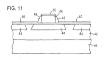
孤立したSOI部分(SOI island)44は、埋め込まれた酸化物層42上に形成される。ゲート電極46は、幅の狭いスペーサ48によってその側壁について保護される。このスペーサ48は、例えば窒化シリコンによって構成することができる。
ソース/ドレインの表面上の酸化膜50の成長は、SOI膜44中で生成されるストレスに、さらにストレスを加える。これにより、キャリア移動度が改善される。その後、標準的なCMOS処理が続行されてもよい。
Claims (10)
- 第1ゲート電極(16)から第1間隔を隔ててn型ドーパントを注入することによって、nチャネルトランジスタ(12)中にソース/ドレイン拡張部(20)を形成するステップと、
第2ゲート電極(16)から前記第1間隔よりも大きい第2間隔を隔ててp型ドーパントを注入することによって、pチャネルトランジスタ(14)中にソース/ドレイン拡張部(26)を形成するステップと、
を含む、同じ基板上にnチャネルトランジスタおよびpチャネルトランジスタを形成する方法。 - 前記nチャネルトランジスタ(12)および前記pチャネルトランジスタ(14)中にソース/ドレイン拡張部(20)、(26)を形成するステップは、第1スペーサ幅に従ってn型ドーパントを注入するステップと、第2スペーサ幅に従ってp型ドーパントを注入するステップとを含む、請求項1記載の方法。
- 前記nチャネルトランジスタ(12)および前記pチャネルトランジスタ(14)の前記ゲート電極(16)上に、前記第1スペーサ幅とほぼ同じ幅を有する第1オフセットスペーサ(18)を形成するステップをさらに含む、請求項2記載の方法。
- 対となるオフセットスペーサ(18)、(22)であって、その合計幅が前記第2スペーサ幅とほぼ同じ幅であるものを形成すべく、前記第1オフセットスペーサ(18)上に第2オフセットスペーサ(22)を形成するステップをさらに含む、請求項3記載の方法。
- 前記n型ドーパントは、前記第1オフセットスペーサ(18)が形成された後、前記n型トランジスタ(12)中の前記ソース/ドレイン拡張部(20)を形成するように注入され、前記p型ドーパントは、前記対となるオフセットスペーサ(18)、(22)が形成された後、前記p型トランジスタ(14)中の前記ソース/ドレイン拡張部(26)を形成するように注入される、請求項4記載の方法。
- 前記第2オフセットスペーサ(22)上に側壁スペーサ(28)を形成するステップと、
n型ドーパントを注入することによって、nチャネルトランジスタ(12)中にソース/ドレイン領域(30)を形成するステップと、
p型ドーパントを注入することによって、pチャネルトランジスタ(14)中にソース/ドレイン領域(32)を形成するステップとをさらに含む、請求項5記載の方法。 - 前記第1オフセットスペーサ(18)は、約60Åから約180Åの間の幅を有する、請求項6記載の方法。
- 前記第2オフセットスペーサ(22)は、約120Åから約240Åの間の幅を有する、請求項7記載の方法。
- 前記nチャネルトランジスタ(12)中の前記ソース/ドレイン拡張部(20)が形成された後であって、前記第2オフセットスペーサ(22)が形成される前に、前記ゲート電極(16)、前記第1オフセットスペーサ(18)および前記基板上に酸化膜を形成するステップをさらに含む、請求項5記載の方法。
- nチャネルトランジスタ(12)およびpチャネルトランジスタ(14)のゲート電極(16)上に第1オフセットスペーサ(18)を形成するステップと、
前記第1オフセットスペーサ(18)の真下の前記基板(10)への注入を前記第1オフセットスペーサ(18)でマスクした状態で、前記nチャネルトランジスタ(14)の前記基板(10)中のみにソース/ドレイン拡張部(20)を注入するステップと、
前記第1オフセットスペーサ(18)上に第2オフセットスペーサ(22)を形成するステップと、
前記第1オフセットスペーサ(18)および第2オフセットスペーサ(22)の真下の前記基板(10)への注入を前記第1オフセットスペーサ(18)および第2オフセットスペーサ(22)でマスクした状態で、前記pチャネルトランジスタ(14)の前記基板中のみにソース/ドレイン拡張部(22)を注入するステップと、
を含む、基板およびnチャネルトランジスタとpチャネルトランジスタを備える半導体デバイスを形成する方法。
Applications Claiming Priority (2)
| Application Number | Priority Date | Filing Date | Title |
|---|---|---|---|
| US10/014,426 US6562676B1 (en) | 2001-12-14 | 2001-12-14 | Method of forming differential spacers for individual optimization of n-channel and p-channel transistors |
| PCT/US2002/039782 WO2003052799A2 (en) | 2001-12-14 | 2002-12-11 | A method of forming differential spacers for individual optimization of n-channel and p-channel transistors |
Publications (2)
| Publication Number | Publication Date |
|---|---|
| JP2005513774A true JP2005513774A (ja) | 2005-05-12 |
| JP2005513774A5 JP2005513774A5 (ja) | 2006-02-02 |
Family
ID=21765406
Family Applications (1)
| Application Number | Title | Priority Date | Filing Date |
|---|---|---|---|
| JP2003553602A Pending JP2005513774A (ja) | 2001-12-14 | 2002-12-11 | Nチャネルトランジスタおよびpチャネルトランジスタのそれぞれを最適化する、異なるスペーサを形成する方法 |
Country Status (8)
| Country | Link |
|---|---|
| US (1) | US6562676B1 (ja) |
| EP (1) | EP1454342A2 (ja) |
| JP (1) | JP2005513774A (ja) |
| KR (1) | KR100941742B1 (ja) |
| CN (1) | CN1307689C (ja) |
| AU (1) | AU2002359686A1 (ja) |
| TW (1) | TWI260731B (ja) |
| WO (1) | WO2003052799A2 (ja) |
Cited By (2)
| Publication number | Priority date | Publication date | Assignee | Title |
|---|---|---|---|---|
| JP2010509776A (ja) * | 2006-11-10 | 2010-03-25 | ラム リサーチ コーポレーション | 除去可能なスペーサ |
| WO2010140244A1 (ja) * | 2009-06-05 | 2010-12-09 | ルネサスエレクトロニクス株式会社 | 半導体装置およびその製造方法 |
Families Citing this family (17)
| Publication number | Priority date | Publication date | Assignee | Title |
|---|---|---|---|---|
| US6828219B2 (en) * | 2002-03-22 | 2004-12-07 | Winbond Electronics Corporation | Stacked spacer structure and process |
| US7416927B2 (en) * | 2002-03-26 | 2008-08-26 | Infineon Technologies Ag | Method for producing an SOI field effect transistor |
| US6894353B2 (en) * | 2002-07-31 | 2005-05-17 | Freescale Semiconductor, Inc. | Capped dual metal gate transistors for CMOS process and method for making the same |
| US6677201B1 (en) * | 2002-10-01 | 2004-01-13 | Texas Instruments Incorporated | Method of fabricating thermal CVD oxynitride and BTBAS nitride sidewall spacer for metal oxide semiconductor transistors |
| US6969646B2 (en) * | 2003-02-10 | 2005-11-29 | Chartered Semiconductor Manufacturing Ltd. | Method of activating polysilicon gate structure dopants after offset spacer deposition |
| US6967143B2 (en) * | 2003-04-30 | 2005-11-22 | Freescale Semiconductor, Inc. | Semiconductor fabrication process with asymmetrical conductive spacers |
| US7192876B2 (en) * | 2003-05-22 | 2007-03-20 | Freescale Semiconductor, Inc. | Transistor with independent gate structures |
| US20050059260A1 (en) * | 2003-09-15 | 2005-03-17 | Haowen Bu | CMOS transistors and methods of forming same |
| US7033897B2 (en) * | 2003-10-23 | 2006-04-25 | Texas Instruments Incorporated | Encapsulated spacer with low dielectric constant material to reduce the parasitic capacitance between gate and drain in CMOS technology |
| JP4796747B2 (ja) * | 2003-12-25 | 2011-10-19 | 富士通セミコンダクター株式会社 | Cmos半導体装置の製造方法 |
| US20050275034A1 (en) * | 2004-04-08 | 2005-12-15 | International Business Machines Corporation | A manufacturable method and structure for double spacer cmos with optimized nfet/pfet performance |
| US7687861B2 (en) * | 2005-10-12 | 2010-03-30 | Taiwan Semiconductor Manufacturing Company, Ltd. | Silicided regions for NMOS and PMOS devices |
| DE102009021490B4 (de) * | 2009-05-15 | 2013-04-04 | Globalfoundries Dresden Module One Llc & Co. Kg | Mehrschrittabscheidung eines Abstandshaltermaterials zur Reduzierung der Ausbildung von Hohlräumen in einem dielektrischen Material einer Kontaktebene eines Halbleiterbauelements |
| DE102010064284B4 (de) * | 2010-12-28 | 2016-03-31 | GLOBALFOUNDRIES Dresden Module One Ltd. Liability Company & Co. KG | Verfahren zur Herstellung eines Transistors mit einer eingebetteten Sigma-förmigen Halbleiterlegierung mit erhöhter Gleichmäßigkeit |
| US20130026575A1 (en) * | 2011-07-28 | 2013-01-31 | Synopsys, Inc. | Threshold adjustment of transistors by controlled s/d underlap |
| US10038063B2 (en) | 2014-06-10 | 2018-07-31 | International Business Machines Corporation | Tunable breakdown voltage RF FET devices |
| JP6275559B2 (ja) | 2014-06-13 | 2018-02-07 | ルネサスエレクトロニクス株式会社 | 半導体装置およびその製造方法 |
Citations (5)
| Publication number | Priority date | Publication date | Assignee | Title |
|---|---|---|---|---|
| JPH09167804A (ja) * | 1995-12-15 | 1997-06-24 | Hitachi Ltd | 半導体装置及びその製造方法 |
| JPH09172176A (ja) * | 1995-11-21 | 1997-06-30 | Texas Instr Inc <Ti> | Mosデバイス製造方法 |
| JP2000307015A (ja) * | 1999-04-22 | 2000-11-02 | Oki Electric Ind Co Ltd | デュアルゲートcmosfetの製造方法 |
| JP2001110913A (ja) * | 1999-10-06 | 2001-04-20 | Nec Corp | 半導体装置の製造方法 |
| JP2001516154A (ja) * | 1997-09-05 | 2001-09-25 | アドバンスト・マイクロ・ディバイシズ・インコーポレイテッド | 個別に最適化されたnチャネルおよびpチャネルトランジスタ性能のための除去可能なサイドウォールスペーサを用いるcmosプロセス |
Family Cites Families (7)
| Publication number | Priority date | Publication date | Assignee | Title |
|---|---|---|---|---|
| KR100186514B1 (ko) * | 1996-06-10 | 1999-04-15 | 문정환 | 반도체 소자의 격리영역 형성방법 |
| JP3114654B2 (ja) * | 1997-06-05 | 2000-12-04 | 日本電気株式会社 | 半導体装置の製造方法 |
| US5943565A (en) * | 1997-09-05 | 1999-08-24 | Advanced Micro Devices, Inc. | CMOS processing employing separate spacers for independently optimized transistor performance |
| US6124610A (en) * | 1998-06-26 | 2000-09-26 | Advanced Micro Devices, Inc. | Isotropically etching sidewall spacers to be used for both an NMOS source/drain implant and a PMOS LDD implant |
| US5981325A (en) * | 1999-04-26 | 1999-11-09 | United Semiconductor Corp. | Method for manufacturing CMOS |
| KR20010065744A (ko) * | 1999-12-30 | 2001-07-11 | 박종섭 | 모스형 트랜지스터 제조방법 |
| TW459294B (en) * | 2000-10-26 | 2001-10-11 | United Microelectronics Corp | Self-aligned offset gate structure and its manufacturing method |
-
2001
- 2001-12-14 US US10/014,426 patent/US6562676B1/en not_active Expired - Lifetime
-
2002
- 2002-12-11 KR KR1020047009262A patent/KR100941742B1/ko active IP Right Grant
- 2002-12-11 JP JP2003553602A patent/JP2005513774A/ja active Pending
- 2002-12-11 AU AU2002359686A patent/AU2002359686A1/en not_active Abandoned
- 2002-12-11 EP EP02794239A patent/EP1454342A2/en not_active Ceased
- 2002-12-11 CN CNB028249763A patent/CN1307689C/zh not_active Expired - Lifetime
- 2002-12-11 WO PCT/US2002/039782 patent/WO2003052799A2/en active Application Filing
- 2002-12-13 TW TW091136063A patent/TWI260731B/zh not_active IP Right Cessation
Patent Citations (5)
| Publication number | Priority date | Publication date | Assignee | Title |
|---|---|---|---|---|
| JPH09172176A (ja) * | 1995-11-21 | 1997-06-30 | Texas Instr Inc <Ti> | Mosデバイス製造方法 |
| JPH09167804A (ja) * | 1995-12-15 | 1997-06-24 | Hitachi Ltd | 半導体装置及びその製造方法 |
| JP2001516154A (ja) * | 1997-09-05 | 2001-09-25 | アドバンスト・マイクロ・ディバイシズ・インコーポレイテッド | 個別に最適化されたnチャネルおよびpチャネルトランジスタ性能のための除去可能なサイドウォールスペーサを用いるcmosプロセス |
| JP2000307015A (ja) * | 1999-04-22 | 2000-11-02 | Oki Electric Ind Co Ltd | デュアルゲートcmosfetの製造方法 |
| JP2001110913A (ja) * | 1999-10-06 | 2001-04-20 | Nec Corp | 半導体装置の製造方法 |
Cited By (4)
| Publication number | Priority date | Publication date | Assignee | Title |
|---|---|---|---|---|
| JP2010509776A (ja) * | 2006-11-10 | 2010-03-25 | ラム リサーチ コーポレーション | 除去可能なスペーサ |
| WO2010140244A1 (ja) * | 2009-06-05 | 2010-12-09 | ルネサスエレクトロニクス株式会社 | 半導体装置およびその製造方法 |
| JP5374585B2 (ja) * | 2009-06-05 | 2013-12-25 | ルネサスエレクトロニクス株式会社 | 半導体装置およびその製造方法 |
| US9449883B2 (en) | 2009-06-05 | 2016-09-20 | Renesas Electronics Corporation | Semiconductor device and method for manufacturing the same |
Also Published As
| Publication number | Publication date |
|---|---|
| TWI260731B (en) | 2006-08-21 |
| KR20040064305A (ko) | 2004-07-16 |
| KR100941742B1 (ko) | 2010-02-11 |
| WO2003052799A3 (en) | 2003-08-14 |
| US6562676B1 (en) | 2003-05-13 |
| AU2002359686A8 (en) | 2003-06-30 |
| CN1605115A (zh) | 2005-04-06 |
| CN1307689C (zh) | 2007-03-28 |
| EP1454342A2 (en) | 2004-09-08 |
| WO2003052799A2 (en) | 2003-06-26 |
| TW200303069A (en) | 2003-08-16 |
| AU2002359686A1 (en) | 2003-06-30 |
Similar Documents
| Publication | Publication Date | Title |
|---|---|---|
| US6686233B2 (en) | Integration of high voltage self-aligned MOS components | |
| JP2663402B2 (ja) | Cmos集積回路デバイスの製造方法 | |
| JP2005513774A (ja) | Nチャネルトランジスタおよびpチャネルトランジスタのそれぞれを最適化する、異なるスペーサを形成する方法 | |
| JPH08250728A (ja) | 電界効果型半導体装置及びその製造方法 | |
| JP3394408B2 (ja) | 半導体装置及びその製造方法 | |
| US6858907B2 (en) | Method of fabricating semiconductor device having notched gate | |
| KR100638546B1 (ko) | 트랜지스터 구조물 형성방법 및 트랜지스터 구조물 | |
| US6797555B1 (en) | Direct implantation of fluorine into the channel region of a PMOS device | |
| US6617214B2 (en) | Integrated circuit structure and method therefore | |
| JP3114654B2 (ja) | 半導体装置の製造方法 | |
| KR20050069579A (ko) | 반도체 소자 및 그의 제조방법 | |
| JP3425043B2 (ja) | Mis型半導体装置の製造方法 | |
| US6451675B1 (en) | Semiconductor device having varied dopant density regions | |
| KR0155536B1 (ko) | BiCMOS 소자의 제조방법 | |
| JPH0637309A (ja) | 半導体装置の製造方法 | |
| JPH0738095A (ja) | 半導体装置及びその製造方法 | |
| JPH06268057A (ja) | 半導体装置の製造方法 | |
| JPS6025028B2 (ja) | 半導体装置の製造方法 | |
| JP2003249567A (ja) | 半導体装置 | |
| KR950000151B1 (ko) | Itldd 구조의 반도체장치의 제조방법 | |
| KR100334968B1 (ko) | 매몰 채널 pmos 트랜지스터 제조 방법 | |
| KR100386460B1 (ko) | 씨모스 트랜지스터의 게이트 전극 형성방법 | |
| JPH06196642A (ja) | 半導体装置及びその製造方法 | |
| KR950003239B1 (ko) | 엘디디구조 씨모스장치의 제조방법 | |
| KR100233269B1 (ko) | 측면 전도가 없는 트랜지스터를 갖는 반도체 장치 및 그 제조 방법 |
Legal Events
| Date | Code | Title | Description |
|---|---|---|---|
| A521 | Written amendment |
Free format text: JAPANESE INTERMEDIATE CODE: A523 Effective date: 20051207 |
|
| A621 | Written request for application examination |
Free format text: JAPANESE INTERMEDIATE CODE: A621 Effective date: 20051207 |
|
| A131 | Notification of reasons for refusal |
Free format text: JAPANESE INTERMEDIATE CODE: A131 Effective date: 20090825 |
|
| A601 | Written request for extension of time |
Free format text: JAPANESE INTERMEDIATE CODE: A601 Effective date: 20091124 |
|
| A602 | Written permission of extension of time |
Free format text: JAPANESE INTERMEDIATE CODE: A602 Effective date: 20091201 |
|
| A601 | Written request for extension of time |
Free format text: JAPANESE INTERMEDIATE CODE: A601 Effective date: 20091225 |
|
| A602 | Written permission of extension of time |
Free format text: JAPANESE INTERMEDIATE CODE: A602 Effective date: 20100107 |
|
| A601 | Written request for extension of time |
Free format text: JAPANESE INTERMEDIATE CODE: A601 Effective date: 20100125 |
|
| A602 | Written permission of extension of time |
Free format text: JAPANESE INTERMEDIATE CODE: A602 Effective date: 20100205 |
|
| A521 | Written amendment |
Free format text: JAPANESE INTERMEDIATE CODE: A523 Effective date: 20100225 |
|
| A02 | Decision of refusal |
Free format text: JAPANESE INTERMEDIATE CODE: A02 Effective date: 20100413 |
|
| RD03 | Notification of appointment of power of attorney |
Free format text: JAPANESE INTERMEDIATE CODE: A7423 Effective date: 20100421 |
|
| A521 | Written amendment |
Free format text: JAPANESE INTERMEDIATE CODE: A523 Effective date: 20100813 |
|
| RD05 | Notification of revocation of power of attorney |
Free format text: JAPANESE INTERMEDIATE CODE: A7425 Effective date: 20100902 |
|
| A911 | Transfer to examiner for re-examination before appeal (zenchi) |
Free format text: JAPANESE INTERMEDIATE CODE: A911 Effective date: 20100929 |
|
| A912 | Re-examination (zenchi) completed and case transferred to appeal board |
Free format text: JAPANESE INTERMEDIATE CODE: A912 Effective date: 20101022 |