JP2005293808A - 試験装置、位相調整方法、及びメモリコントローラ - Google Patents
試験装置、位相調整方法、及びメモリコントローラ Download PDFInfo
- Publication number
- JP2005293808A JP2005293808A JP2004111494A JP2004111494A JP2005293808A JP 2005293808 A JP2005293808 A JP 2005293808A JP 2004111494 A JP2004111494 A JP 2004111494A JP 2004111494 A JP2004111494 A JP 2004111494A JP 2005293808 A JP2005293808 A JP 2005293808A
- Authority
- JP
- Japan
- Prior art keywords
- signal
- output
- timing
- comparator
- phase adjustment
- Prior art date
- Legal status (The legal status is an assumption and is not a legal conclusion. Google has not performed a legal analysis and makes no representation as to the accuracy of the status listed.)
- Granted
Links
- 238000012360 testing method Methods 0.000 title claims abstract description 239
- 230000015654 memory Effects 0.000 title claims abstract description 170
- 238000000034 method Methods 0.000 title claims description 15
- 230000008859 change Effects 0.000 claims description 20
- 230000003111 delayed effect Effects 0.000 claims description 17
- 230000001934 delay Effects 0.000 claims description 10
- 238000001514 detection method Methods 0.000 claims description 10
- 230000001360 synchronised effect Effects 0.000 claims description 3
- 230000000630 rising effect Effects 0.000 claims 1
- 238000010586 diagram Methods 0.000 description 8
- 230000005540 biological transmission Effects 0.000 description 7
- 238000004891 communication Methods 0.000 description 5
- 230000006870 function Effects 0.000 description 3
- 238000012986 modification Methods 0.000 description 3
- 230000004048 modification Effects 0.000 description 3
- 230000000737 periodic effect Effects 0.000 description 2
- 238000010998 test method Methods 0.000 description 2
- 230000002457 bidirectional effect Effects 0.000 description 1
- 230000007423 decrease Effects 0.000 description 1
- 230000001419 dependent effect Effects 0.000 description 1
- 238000005259 measurement Methods 0.000 description 1
- 230000010363 phase shift Effects 0.000 description 1
- 230000004044 response Effects 0.000 description 1
- 238000005070 sampling Methods 0.000 description 1
- 238000012546 transfer Methods 0.000 description 1
Images
Classifications
-
- G—PHYSICS
- G11—INFORMATION STORAGE
- G11C—STATIC STORES
- G11C29/00—Checking stores for correct operation ; Subsequent repair; Testing stores during standby or offline operation
- G11C29/02—Detection or location of defective auxiliary circuits, e.g. defective refresh counters
- G11C29/028—Detection or location of defective auxiliary circuits, e.g. defective refresh counters with adaption or trimming of parameters
-
- G—PHYSICS
- G11—INFORMATION STORAGE
- G11C—STATIC STORES
- G11C29/00—Checking stores for correct operation ; Subsequent repair; Testing stores during standby or offline operation
- G11C29/04—Detection or location of defective memory elements, e.g. cell constructio details, timing of test signals
- G11C29/50—Marginal testing, e.g. race, voltage or current testing
- G11C29/50012—Marginal testing, e.g. race, voltage or current testing of timing
-
- G—PHYSICS
- G11—INFORMATION STORAGE
- G11C—STATIC STORES
- G11C29/00—Checking stores for correct operation ; Subsequent repair; Testing stores during standby or offline operation
- G11C29/56—External testing equipment for static stores, e.g. automatic test equipment [ATE]; Interfaces therefor
-
- G—PHYSICS
- G11—INFORMATION STORAGE
- G11C—STATIC STORES
- G11C29/00—Checking stores for correct operation ; Subsequent repair; Testing stores during standby or offline operation
- G11C29/56—External testing equipment for static stores, e.g. automatic test equipment [ATE]; Interfaces therefor
- G11C29/56012—Timing aspects, clock generation, synchronisation
-
- G—PHYSICS
- G11—INFORMATION STORAGE
- G11C—STATIC STORES
- G11C29/00—Checking stores for correct operation ; Subsequent repair; Testing stores during standby or offline operation
- G11C29/56—External testing equipment for static stores, e.g. automatic test equipment [ATE]; Interfaces therefor
- G11C2029/5602—Interface to device under test
Landscapes
- Tests Of Electronic Circuits (AREA)
- For Increasing The Reliability Of Semiconductor Memories (AREA)
- Manipulation Of Pulses (AREA)
- Stabilization Of Oscillater, Synchronisation, Frequency Synthesizers (AREA)
Abstract
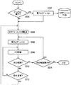
【解決手段】本発明の試験装置は、被試験メモリから出力された出力信号の出力値を、ストローブ信号のタイミングで取得するタイミングコンパレータと、タイミングコンパレータが取得した出力値を予め生成された期待値と比較して、比較結果を出力する論理比較器と、論理比較器が出力した比較結果に基づいて、ストローブ信号のタイミングを調整する位相調整制御回路とを備える。
【選択図】図1
Description
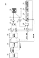
102 タイミング発生器
104 パターン発生器
106 波形整形器
108 可変遅延回路
110 可変遅延回路
112 SRラッチ
114 ドライバ
116 レベルコンパレータ
118 可変遅延回路
120 タイミングコンパレータ
122 論理比較器
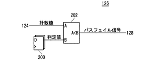
124 フェイルカウンタ
126 判定回路
128 位相調整制御回路
200 判定値レジスタ
202 計数値比較器
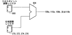
900 クロスポイント調整レジスタ
904 加算器
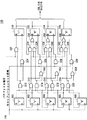
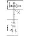
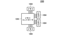
1000 メモリ制御システム
1002 メモリコントローラ
1004 メモリ
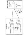
1100 送受信制御部
1104 ストローブ信号発生器
1116 レベルコンパレータ
1118 可変遅延回路
1120 タイミングコンパレータ
1122 論理比較器
1124 フェイルカウンタ
1126 判定回路
1128 位相調整制御回路
1130 温度検出部
1132 リキャリブレーション制御部
1134 リキャリブレーション間隔制御部
Claims (14)
- 被試験メモリを試験する試験装置であって、
前記被試験メモリから出力された出力信号の出力値を、ストローブ信号のタイミングで取得するタイミングコンパレータと、
前記タイミングコンパレータが取得した前記出力値を予め生成された期待値と比較して、比較結果を出力する論理比較器と、
前記論理比較器が出力した前記比較結果に基づいて、前記ストローブ信号のタイミングを調整する位相調整制御回路と
を備える試験装置。 - 前記ストローブ信号を遅延させて前記タイミングコンパレータに供給する第1可変遅延回路
をさらに備え、
前記位相調整制御回路は、前記論理比較器が出力した前記比較結果に基づいて、前記第1可変遅延回路による遅延量を設定する
請求項1に記載の試験装置。 - 前記論理比較器が前記比較結果として出力した、前記出力値と前記期待値とが一致しないことを示すフェイルデータの数を計数するフェイルカウンタと、
前記フェイルカウンタが計数した前記フェイルデータの数を、予め定められた判定値と比較して、判定結果を出力する判定回路と
をさらに備え、
前記位相調整制御回路は、前記判定回路が出力した前記判定結果に基づいて、前記第1可変遅延回路による遅延量を設定する
請求項2に記載の試験装置。 - 前記位相調整制御回路は、2進数データで示される前記第1可変遅延回路による前記遅延量を、前記判定回路が出力した前記判定結果に基づいてバイナリサーチにより上位ビットから順に決定していく
請求項3に記載の試験装置。 - セット信号のタイミングで試験パターン信号を立ち上げ、リセット信号のタイミングで前記試験パターン信号を立ち下げて、前記試験パターン信号を前記被試験メモリに供給するSRラッチと、
前記セット信号を遅延させて前記SRラッチに供給する第2可変遅延回路と、
前記リセット信号を遅延させて前記SRラッチに供給する第3可変遅延回路と
をさらに備え、
前記タイミングコンパレータは、前記試験パターン信号に対応して前記被試験メモリから出力された出力信号の出力値を、前記被試験メモリの内部クロックと同期した前記ストローブ信号のタイミングで取得し、
前記論理比較器は、前記タイミングコンパレータが取得した前記出力値を前記期待値と比較して、比較結果を出力し、
前記位相調整制御回路は、前記論理比較器が出力した前記比較結果に基づいて、前記第2可変遅延回路及び前記3可変遅延回路による遅延量を設定する
請求項1に記載の試験装置。 - 前記被試験メモリの温度又は前記被試験メモリの周囲の温度の変化を検出する温度検出部と、
前記温度検出部が検出した温度変化が予め定められた温度変化以上である場合に、前記ストローブ信号のタイミングを再度調整させるリキャリブレーション制御部と
をさらに備える請求項1に記載の試験装置。 - 前記被試験メモリに対するデータの書き込み又は読み出しを連続して行った場合に、前記論理比較器が経過時間毎に出力した前記比較結果に基づいて、前記ストローブ信号のタイミングを再調整すべき時間間隔を測定するリキャリブレーション間隔制御部
をさらに備える請求項1に記載の試験装置。 - 被試験メモリから出力された出力信号とストローブ信号とのタイミングを調整する位相調整方法であって、
前記被試験メモリから出力された前記出力信号の出力値を、前記ストローブ信号のタイミングで取得する出力値取得段階と、
取得された前記出力値を予め生成された期待値と比較して、比較結果を出力する段階と、
前記比較結果に基づいて、前記ストローブ信号のタイミングを調整する段階と
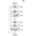
を備える位相調整方法。 - 前記被試験メモリに試験パターン信号を低速で書き込む低速書込段階と、
前記試験パターン信号に対応した前記出力信号を前記被試験メモリから高速で読み出す第1高速読出段階と
をさらに備え、
前記出力値取得段階は、前記第1高速読出段階において読み出された前記出力信号の前記出力値を、前記ストローブ信号のタイミングで取得する段階を有する
請求項8に記載の位相調整方法。 - 前記低速書込段階は、前記被試験メモリのスキャン入出力端子から前記試験パターン信号を書き込む段階を有し、
前記第1高速読出段階は、前記被試験メモリのデータ入出力端子から前記試験パターン信号を読み出す段階を有する
請求項9に記載の位相調整方法。 - セット信号のタイミングで試験パターン信号を立ち上げ、リセット信号のタイミングで前記試験パターン信号を立ち下げて、前記試験パターン信号を前記被試験メモリに高速で書き込む高速書込段階と、
前記試験パターン信号に対応した前記出力信号を前記被試験メモリから高速で読み出す第2高速読出段階と、
前記第2高速読出段階において読み出された前記出力信号の出力値を、前記ストローブ信号のタイミングで取得する段階と、
取得された前記出力値を予め生成された前記期待値と比較して、比較結果を出力する段階と、
前記比較結果に基づいて、前記セット信号及び前記リセット信号のタイミングを調整する段階と
をさらに備える請求項8に記載の位相調整方法。 - 前記高速書込段階は、前記被試験メモリのデータ入出力端子から前記試験パターン信号を書き込む段階を有し、
前記第2高速読出段階は、前記被試験メモリのデータ入出力端子から前記試験パターン信号を読み出す段階を有する
請求項11に記載の位相調整方法。 - メモリのデータの書き込み及び読み出しを制御するメモリコントローラであって、
前記メモリから読み出された出力信号の出力値を、ストローブ信号のタイミングで取得するタイミングコンパレータと、
前記タイミングコンパレータが取得した前記出力値を予め生成された期待値と比較して、比較結果を出力する論理比較器と、
前記論理比較器が出力した前記比較結果に基づいて、前記ストローブ信号のタイミングを調整する位相調整制御回路と、
前記メモリの温度又は前記メモリの周囲の温度の変化を検出する温度検出部と、
前記温度検出部が検出した温度変化が予め定められた温度変化以上である場合に、前記ストローブ信号のタイミングを再度調整させるリキャリブレーション制御部と
を備えるメモリコントローラ。 - メモリのデータの書き込み及び読み出しを制御するメモリコントローラであって、
前記メモリから読み出された出力信号の出力値を、ストローブ信号のタイミングで取得するタイミングコンパレータと、
前記タイミングコンパレータが取得した前記出力値を予め生成された期待値と比較して、比較結果を出力する論理比較器と、
前記論理比較器が出力した前記比較結果に基づいて、前記ストローブ信号のタイミングを調整する位相調整制御回路と、
前記メモリに対するデータの書き込み又は読み出しを連続して行った場合に、前記論理比較器が経過時間毎に出力した前記比較結果に基づいて、前記ストローブ信号のタイミングを再調整すべき時間間隔を測定するリキャリブレーション間隔制御部と
を備えるメモリコントローラ。
Priority Applications (6)
| Application Number | Priority Date | Filing Date | Title |
|---|---|---|---|
| JP2004111494A JP4451189B2 (ja) | 2004-04-05 | 2004-04-05 | 試験装置、位相調整方法、及びメモリコントローラ |
| KR1020067023285A KR100840800B1 (ko) | 2004-04-05 | 2005-03-25 | 시험 장치, 위상 조정 방법, 및 메모리 제어기 |
| CNB2005800101694A CN100505107C (zh) | 2004-04-05 | 2005-03-25 | 测试装置、相位调整方法及存储器控制器 |
| DE112005000745T DE112005000745T5 (de) | 2004-04-05 | 2005-03-25 | Testgerät, Phaseneinstellverfahren und Speichersteuerung |
| PCT/JP2005/005547 WO2005098868A1 (ja) | 2004-04-05 | 2005-03-25 | 試験装置、位相調整方法、及びメモリコントローラ |
| US11/180,895 US7266738B2 (en) | 2004-04-05 | 2005-07-13 | Test apparatus, phase adjusting method and memory controller |
Applications Claiming Priority (1)
| Application Number | Priority Date | Filing Date | Title |
|---|---|---|---|
| JP2004111494A JP4451189B2 (ja) | 2004-04-05 | 2004-04-05 | 試験装置、位相調整方法、及びメモリコントローラ |
Publications (3)
| Publication Number | Publication Date |
|---|---|
| JP2005293808A true JP2005293808A (ja) | 2005-10-20 |
| JP2005293808A5 JP2005293808A5 (ja) | 2008-08-21 |
| JP4451189B2 JP4451189B2 (ja) | 2010-04-14 |
Family
ID=35125332
Family Applications (1)
| Application Number | Title | Priority Date | Filing Date |
|---|---|---|---|
| JP2004111494A Expired - Fee Related JP4451189B2 (ja) | 2004-04-05 | 2004-04-05 | 試験装置、位相調整方法、及びメモリコントローラ |
Country Status (6)
| Country | Link |
|---|---|
| US (1) | US7266738B2 (ja) |
| JP (1) | JP4451189B2 (ja) |
| KR (1) | KR100840800B1 (ja) |
| CN (1) | CN100505107C (ja) |
| DE (1) | DE112005000745T5 (ja) |
| WO (1) | WO2005098868A1 (ja) |
Cited By (7)
| Publication number | Priority date | Publication date | Assignee | Title |
|---|---|---|---|---|
| JP2009032310A (ja) * | 2007-07-25 | 2009-02-12 | Fujitsu Ltd | 高速製品の試験方法及び装置 |
| WO2010023924A1 (ja) * | 2008-08-28 | 2010-03-04 | 株式会社アドバンテスト | 相互接続基板、スキュー測定方法および試験装置 |
| WO2010058441A1 (ja) * | 2008-11-19 | 2010-05-27 | 株式会社アドバンテスト | 試験装置、試験方法、および、プログラム |
| JP2011060392A (ja) * | 2009-09-11 | 2011-03-24 | Nec Corp | 半導体記憶装置の試験方法 |
| CN104764914A (zh) * | 2014-01-03 | 2015-07-08 | 致茂电子股份有限公司 | 误差补偿方法与应用此方法的自动测试设备 |
| JP2015532488A (ja) * | 2012-10-05 | 2015-11-09 | クアルコム,インコーポレイテッド | 外部メモリチューニングシーケンスの最適使用のためのアルゴリズム |
| JP2017122718A (ja) * | 2015-12-09 | 2017-07-13 | 致茂電子股▲分▼有限公司Chroma Ate Inc. | パルス発生装置及びパルス発生装置の較正方法 |
Families Citing this family (30)
| Publication number | Priority date | Publication date | Assignee | Title |
|---|---|---|---|---|
| US7254763B2 (en) * | 2004-09-01 | 2007-08-07 | Agere Systems Inc. | Built-in self test for memory arrays using error correction coding |
| KR100639678B1 (ko) * | 2004-11-16 | 2006-10-30 | 삼성전자주식회사 | 테스트 장치 |
| US7573957B2 (en) * | 2005-09-23 | 2009-08-11 | Teradyne, Inc. | Strobe technique for recovering a clock in a digital signal |
| US7856578B2 (en) * | 2005-09-23 | 2010-12-21 | Teradyne, Inc. | Strobe technique for test of digital signal timing |
| US7574632B2 (en) * | 2005-09-23 | 2009-08-11 | Teradyne, Inc. | Strobe technique for time stamping a digital signal |
| JP4949707B2 (ja) * | 2006-03-22 | 2012-06-13 | ルネサスエレクトロニクス株式会社 | 半導体装置及びそのテスト方法 |
| US7603246B2 (en) * | 2006-03-31 | 2009-10-13 | Nvidia Corporation | Data interface calibration |
| US7715251B2 (en) * | 2006-10-25 | 2010-05-11 | Hewlett-Packard Development Company, L.P. | Memory access strobe configuration system and process |
| US7797121B2 (en) * | 2007-06-07 | 2010-09-14 | Advantest Corporation | Test apparatus, and device for calibration |
| WO2009025020A1 (ja) * | 2007-08-20 | 2009-02-26 | Advantest Corporation | 試験装置、試験方法、および、製造方法 |
| US8521979B2 (en) | 2008-05-29 | 2013-08-27 | Micron Technology, Inc. | Memory systems and methods for controlling the timing of receiving read data |
| US8289760B2 (en) | 2008-07-02 | 2012-10-16 | Micron Technology, Inc. | Multi-mode memory device and method having stacked memory dice, a logic die and a command processing circuit and operating in direct and indirect modes |
| US7855931B2 (en) | 2008-07-21 | 2010-12-21 | Micron Technology, Inc. | Memory system and method using stacked memory device dice, and system using the memory system |
| US8756486B2 (en) | 2008-07-02 | 2014-06-17 | Micron Technology, Inc. | Method and apparatus for repairing high capacity/high bandwidth memory devices |
| US7808849B2 (en) * | 2008-07-08 | 2010-10-05 | Nvidia Corporation | Read leveling of memory units designed to receive access requests in a sequential chained topology |
| JP5171442B2 (ja) * | 2008-07-08 | 2013-03-27 | 株式会社アドバンテスト | マルチストローブ回路および試験装置 |
| US7796465B2 (en) * | 2008-07-09 | 2010-09-14 | Nvidia Corporation | Write leveling of memory units designed to receive access requests in a sequential chained topology |
| US8461884B2 (en) * | 2008-08-12 | 2013-06-11 | Nvidia Corporation | Programmable delay circuit providing for a wide span of delays |
| US8274272B2 (en) * | 2009-02-06 | 2012-09-25 | Advanced Micro Devices, Inc. | Programmable delay module testing device and methods thereof |
| JP5477062B2 (ja) * | 2010-03-08 | 2014-04-23 | 富士通セミコンダクター株式会社 | 半導体集積回路の試験装置、試験方法、及びプログラム |
| US8400808B2 (en) | 2010-12-16 | 2013-03-19 | Micron Technology, Inc. | Phase interpolators and push-pull buffers |
| US8612815B2 (en) * | 2011-12-16 | 2013-12-17 | International Business Machines Corporation | Asynchronous circuit with an at-speed built-in self-test (BIST) architecture |
| US9171597B2 (en) | 2013-08-30 | 2015-10-27 | Micron Technology, Inc. | Apparatuses and methods for providing strobe signals to memories |
| CN104616697A (zh) * | 2014-12-17 | 2015-05-13 | 曙光信息产业(北京)有限公司 | Qdr-sram的时钟相位调整方法和装置 |
| US10867642B2 (en) | 2016-05-17 | 2020-12-15 | Taiwan Semiconductor Manufacturing Company Limited | Active random access memory |
| CN114062889B (zh) * | 2020-08-04 | 2024-08-27 | 瑞昱半导体股份有限公司 | 检测电路运行速度的余量的装置 |
| CN113868107B (zh) * | 2021-09-10 | 2024-04-26 | 长沙市致存科技有限责任公司 | 存储产品后端io的自适应调整方法、装置、设备及介质 |
| US11726904B2 (en) | 2021-09-23 | 2023-08-15 | International Business Machines Corporation | Controlled input/output in progress state during testcase processing |
| CN114116581A (zh) * | 2021-10-14 | 2022-03-01 | 北京国科天迅科技有限公司 | 提高高速串行总线突发传输响应性能的方法及装置 |
| KR20240056205A (ko) * | 2022-10-21 | 2024-04-30 | 매그나칩믹스드시그널 유한회사 | 메모리 리페어 장치 |
Family Cites Families (12)
| Publication number | Priority date | Publication date | Assignee | Title |
|---|---|---|---|---|
| JP3636506B2 (ja) * | 1995-06-19 | 2005-04-06 | 株式会社アドバンテスト | 半導体試験装置 |
| JP3607325B2 (ja) * | 1994-09-22 | 2005-01-05 | 株式会社アドバンテスト | 半導体試験装置用比較回路 |
| US5732047A (en) * | 1995-12-12 | 1998-03-24 | Advantest Corporation | Timing comparator circuit for use in device testing apparatus |
| JPH09166646A (ja) * | 1995-12-15 | 1997-06-24 | Nec Corp | 半導体装置 |
| TW343282B (en) * | 1996-06-14 | 1998-10-21 | Adoban Tesuto Kk | Testing device for a semiconductor device |
| JP3718374B2 (ja) * | 1999-06-22 | 2005-11-24 | 株式会社東芝 | メモリ混載半導体集積回路装置及びそのテスト方法 |
| JP3453133B2 (ja) * | 1999-08-16 | 2003-10-06 | 株式会社アドバンテスト | Ic試験装置のタイミング校正方法及びその校正方法を用いた校正機能を有するic試験装置 |
| JP2001222897A (ja) * | 2000-02-04 | 2001-08-17 | Advantest Corp | 半導体試験装置 |
| JP4291494B2 (ja) * | 2000-04-04 | 2009-07-08 | 株式会社アドバンテスト | Ic試験装置のタイミング校正装置 |
| US6377065B1 (en) * | 2000-04-13 | 2002-04-23 | Advantest Corp. | Glitch detection for semiconductor test system |
| JP2002181899A (ja) * | 2000-12-15 | 2002-06-26 | Advantest Corp | タイミング校正方法 |
| JP2003098235A (ja) * | 2001-09-27 | 2003-04-03 | Matsushita Electric Ind Co Ltd | 半導体集積回路およびその検査方法 |
-
2004
- 2004-04-05 JP JP2004111494A patent/JP4451189B2/ja not_active Expired - Fee Related
-
2005
- 2005-03-25 DE DE112005000745T patent/DE112005000745T5/de not_active Withdrawn
- 2005-03-25 CN CNB2005800101694A patent/CN100505107C/zh not_active Expired - Fee Related
- 2005-03-25 WO PCT/JP2005/005547 patent/WO2005098868A1/ja not_active Ceased
- 2005-03-25 KR KR1020067023285A patent/KR100840800B1/ko not_active Expired - Fee Related
- 2005-07-13 US US11/180,895 patent/US7266738B2/en not_active Expired - Lifetime
Cited By (12)
| Publication number | Priority date | Publication date | Assignee | Title |
|---|---|---|---|---|
| JP2009032310A (ja) * | 2007-07-25 | 2009-02-12 | Fujitsu Ltd | 高速製品の試験方法及び装置 |
| WO2010023924A1 (ja) * | 2008-08-28 | 2010-03-04 | 株式会社アドバンテスト | 相互接続基板、スキュー測定方法および試験装置 |
| US7768255B2 (en) | 2008-08-28 | 2010-08-03 | Advantest Corporation | Interconnection substrate, skew measurement method, and test apparatus |
| KR101178069B1 (ko) | 2008-08-28 | 2012-08-30 | 가부시키가이샤 어드밴티스트 | 상호 접속 기판, 스큐 측정 방법 및 시험 장치 |
| JP5475666B2 (ja) * | 2008-08-28 | 2014-04-16 | 株式会社アドバンテスト | スキュー測定方法および試験装置 |
| WO2010058441A1 (ja) * | 2008-11-19 | 2010-05-27 | 株式会社アドバンテスト | 試験装置、試験方法、および、プログラム |
| JPWO2010058441A1 (ja) * | 2008-11-19 | 2012-04-12 | 株式会社アドバンテスト | 試験装置、試験方法、および、プログラム |
| JP2011060392A (ja) * | 2009-09-11 | 2011-03-24 | Nec Corp | 半導体記憶装置の試験方法 |
| JP2015532488A (ja) * | 2012-10-05 | 2015-11-09 | クアルコム,インコーポレイテッド | 外部メモリチューニングシーケンスの最適使用のためのアルゴリズム |
| JP2018125040A (ja) * | 2012-10-05 | 2018-08-09 | クアルコム,インコーポレイテッド | 外部メモリチューニングシーケンスの最適使用のためのアルゴリズム |
| CN104764914A (zh) * | 2014-01-03 | 2015-07-08 | 致茂电子股份有限公司 | 误差补偿方法与应用此方法的自动测试设备 |
| JP2017122718A (ja) * | 2015-12-09 | 2017-07-13 | 致茂電子股▲分▼有限公司Chroma Ate Inc. | パルス発生装置及びパルス発生装置の較正方法 |
Also Published As
| Publication number | Publication date |
|---|---|
| KR20070001264A (ko) | 2007-01-03 |
| CN1938788A (zh) | 2007-03-28 |
| CN100505107C (zh) | 2009-06-24 |
| US7266738B2 (en) | 2007-09-04 |
| DE112005000745T5 (de) | 2007-02-22 |
| KR100840800B1 (ko) | 2008-06-23 |
| US20060041799A1 (en) | 2006-02-23 |
| JP4451189B2 (ja) | 2010-04-14 |
| WO2005098868A1 (ja) | 2005-10-20 |
Similar Documents
| Publication | Publication Date | Title |
|---|---|---|
| JP4451189B2 (ja) | 試験装置、位相調整方法、及びメモリコントローラ | |
| JP3920318B1 (ja) | 試験装置および試験方法 | |
| JP5613666B2 (ja) | 自動試験装置システム用追跡回路及び方法 | |
| JP4878215B2 (ja) | インタフェース回路及びメモリ制御装置 | |
| US7619404B2 (en) | System and method for testing integrated circuit timing margins | |
| US7644324B2 (en) | Semiconductor memory tester | |
| US7078889B2 (en) | Semiconductor test apparatus for testing semiconductor device that produces output data by its internal clock timing | |
| US7222273B2 (en) | Apparatus and method for testing semiconductor memory devices, capable of selectively changing frequencies of test pattern signals | |
| US20100182857A1 (en) | Tester for semiconductor device and semiconductor device | |
| JP5254794B2 (ja) | デジタル信号のタイミングを試験するためのストローブ技法 | |
| JP2008145361A (ja) | 半導体装置 | |
| JPWO2005012930A1 (ja) | 試験装置 | |
| US7135880B2 (en) | Test apparatus | |
| US7206985B2 (en) | Method and apparatus for calibrating a test system for an integrated semiconductor circuit | |
| US10002650B1 (en) | Signal quality detection circuit for generating signal quality detection result according to two-dimensional nominal sampling point pattern and associated signal quality detection method | |
| JPWO2007072738A1 (ja) | 試験装置、調整装置、調整方法、および、調整プログラム | |
| JP4320733B2 (ja) | 半導体試験装置 | |
| JP2009047480A (ja) | 半導体試験装置 | |
| JP2006105636A (ja) | 半導体試験装置およびそのキャリブレーション方法 | |
| JP5249357B2 (ja) | 電子デバイス、試験装置および試験方法 | |
| JPWO2010087009A1 (ja) | 電子デバイス、試験装置および試験方法 | |
| JPWO2007129491A1 (ja) | 試験装置、回路および電子デバイス |
Legal Events
| Date | Code | Title | Description |
|---|---|---|---|
| A621 | Written request for application examination |
Free format text: JAPANESE INTERMEDIATE CODE: A621 Effective date: 20070105 |
|
| A521 | Request for written amendment filed |
Free format text: JAPANESE INTERMEDIATE CODE: A523 Effective date: 20070518 |
|
| A131 | Notification of reasons for refusal |
Free format text: JAPANESE INTERMEDIATE CODE: A131 Effective date: 20090714 |
|
| A521 | Request for written amendment filed |
Free format text: JAPANESE INTERMEDIATE CODE: A523 Effective date: 20090908 |
|
| TRDD | Decision of grant or rejection written | ||
| A01 | Written decision to grant a patent or to grant a registration (utility model) |
Free format text: JAPANESE INTERMEDIATE CODE: A01 Effective date: 20100119 |
|
| A01 | Written decision to grant a patent or to grant a registration (utility model) |
Free format text: JAPANESE INTERMEDIATE CODE: A01 |
|
| A61 | First payment of annual fees (during grant procedure) |
Free format text: JAPANESE INTERMEDIATE CODE: A61 Effective date: 20100127 |
|
| R150 | Certificate of patent or registration of utility model |
Free format text: JAPANESE INTERMEDIATE CODE: R150 |
|
| FPAY | Renewal fee payment (event date is renewal date of database) |
Free format text: PAYMENT UNTIL: 20130205 Year of fee payment: 3 |
|
| FPAY | Renewal fee payment (event date is renewal date of database) |
Free format text: PAYMENT UNTIL: 20130205 Year of fee payment: 3 |
|
| FPAY | Renewal fee payment (event date is renewal date of database) |
Free format text: PAYMENT UNTIL: 20130205 Year of fee payment: 3 |
|
| R250 | Receipt of annual fees |
Free format text: JAPANESE INTERMEDIATE CODE: R250 |
|
| LAPS | Cancellation because of no payment of annual fees |