JP2005293808A - Test apparatus, phase adjustment method and memory controller - Google Patents
Test apparatus, phase adjustment method and memory controller Download PDFInfo
- Publication number
- JP2005293808A JP2005293808A JP2004111494A JP2004111494A JP2005293808A JP 2005293808 A JP2005293808 A JP 2005293808A JP 2004111494 A JP2004111494 A JP 2004111494A JP 2004111494 A JP2004111494 A JP 2004111494A JP 2005293808 A JP2005293808 A JP 2005293808A
- Authority
- JP
- Japan
- Prior art keywords
- signal
- output
- timing
- comparator
- phase adjustment
- Prior art date
- Legal status (The legal status is an assumption and is not a legal conclusion. Google has not performed a legal analysis and makes no representation as to the accuracy of the status listed.)
- Granted
Links
- 238000012360 testing method Methods 0.000 title claims abstract description 239
- 230000015654 memory Effects 0.000 title claims abstract description 170
- 238000000034 method Methods 0.000 title claims description 15
- 230000008859 change Effects 0.000 claims description 20
- 230000003111 delayed effect Effects 0.000 claims description 17
- 230000001934 delay Effects 0.000 claims description 10
- 238000001514 detection method Methods 0.000 claims description 10
- 230000001360 synchronised effect Effects 0.000 claims description 3
- 230000000630 rising effect Effects 0.000 claims 1
- 238000010586 diagram Methods 0.000 description 8
- 230000005540 biological transmission Effects 0.000 description 7
- 238000004891 communication Methods 0.000 description 5
- 230000006870 function Effects 0.000 description 3
- 238000012986 modification Methods 0.000 description 3
- 230000004048 modification Effects 0.000 description 3
- 230000000737 periodic effect Effects 0.000 description 2
- 238000010998 test method Methods 0.000 description 2
- 230000002457 bidirectional effect Effects 0.000 description 1
- 230000007423 decrease Effects 0.000 description 1
- 230000001419 dependent effect Effects 0.000 description 1
- 238000005259 measurement Methods 0.000 description 1
- 230000010363 phase shift Effects 0.000 description 1
- 230000004044 response Effects 0.000 description 1
- 238000005070 sampling Methods 0.000 description 1
- 238000012546 transfer Methods 0.000 description 1
Images
Classifications
-
- G—PHYSICS
- G11—INFORMATION STORAGE
- G11C—STATIC STORES
- G11C29/00—Checking stores for correct operation ; Subsequent repair; Testing stores during standby or offline operation
- G11C29/02—Detection or location of defective auxiliary circuits, e.g. defective refresh counters
- G11C29/028—Detection or location of defective auxiliary circuits, e.g. defective refresh counters with adaption or trimming of parameters
-
- G—PHYSICS
- G11—INFORMATION STORAGE
- G11C—STATIC STORES
- G11C29/00—Checking stores for correct operation ; Subsequent repair; Testing stores during standby or offline operation
- G11C29/04—Detection or location of defective memory elements, e.g. cell constructio details, timing of test signals
- G11C29/50—Marginal testing, e.g. race, voltage or current testing
- G11C29/50012—Marginal testing, e.g. race, voltage or current testing of timing
-
- G—PHYSICS
- G11—INFORMATION STORAGE
- G11C—STATIC STORES
- G11C29/00—Checking stores for correct operation ; Subsequent repair; Testing stores during standby or offline operation
- G11C29/56—External testing equipment for static stores, e.g. automatic test equipment [ATE]; Interfaces therefor
-
- G—PHYSICS
- G11—INFORMATION STORAGE
- G11C—STATIC STORES
- G11C29/00—Checking stores for correct operation ; Subsequent repair; Testing stores during standby or offline operation
- G11C29/56—External testing equipment for static stores, e.g. automatic test equipment [ATE]; Interfaces therefor
- G11C29/56012—Timing aspects, clock generation, synchronisation
-
- G—PHYSICS
- G11—INFORMATION STORAGE
- G11C—STATIC STORES
- G11C29/00—Checking stores for correct operation ; Subsequent repair; Testing stores during standby or offline operation
- G11C29/56—External testing equipment for static stores, e.g. automatic test equipment [ATE]; Interfaces therefor
- G11C2029/5602—Interface to device under test
Landscapes
- Tests Of Electronic Circuits (AREA)
- For Increasing The Reliability Of Semiconductor Memories (AREA)
- Manipulation Of Pulses (AREA)
- Stabilization Of Oscillater, Synchronisation, Frequency Synthesizers (AREA)
Abstract
Description
本発明は、試験装置、位相調整方法、及びメモリコントローラに関する。特に本発明は、被試験メモリを試験する試験装置、被試験メモリから出力された出力信号とストローブ信号とのタイミングを調整する位相調整方法、及びメモリのデータの書き込み及び読み出しを制御するメモリコントローラに関する。 The present invention relates to a test apparatus, a phase adjustment method, and a memory controller. In particular, the present invention relates to a test apparatus that tests a memory under test, a phase adjustment method that adjusts the timing between an output signal output from the memory under test and a strobe signal, and a memory controller that controls writing and reading of data in the memory. .
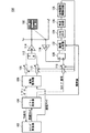
図12は、従来技術に係る試験装置10の構成を示す。試験装置10は、可変遅延回路12、14、22、24、32、及び42、SRラッチ16及び26、ドライバ18及び28、レベルコンパレータ30及び40、並びにタイミングコンパレータ34及び44を備える。
FIG. 12 shows the configuration of a
SRラッチ16は、可変遅延回路12によって遅延されたセット信号及び可変遅延回路14によって遅延されたリセット信号に基づいて試験パターン信号を発生出力し、ドライバ18を介して被試験メモリ50に供給する。SRラッチ26は、可変遅延回路22によって遅延されたセット信号及び可変遅延回路24によって遅延されたリセット信号に基づいて試験パターン信号を発生出力し、ドライバ28を介して被試験メモリ50に供給する。また、タイミングコンパレータ34は、レベルコンパレータ30を介して被試験メモリ50から出力された出力信号を受け取り、可変遅延回路32により遅延されたストローブ信号に基づいて出力値をサンプリングする。タイミングコンパレータ44は、レベルコンパレータ40を介して被試験メモリ50から出力された出力信号を受け取り、可変遅延回路42により遅延されたストローブ信号に基づいて出力値をサンプリングする。
The
そして、タイミングコンパレータ34又は44によってサンプリングされた出力値は、論理比較器によって、予め生成された期待値と比較される。そして、試験装置10は、論理比較器による比較結果に基づいて、被試験メモリ50の良否を判定する。
The output value sampled by the
試験装置10では、被試験メモリ50の試験を実行する前に次にような位相調整を行う。まず、ドライバ18及び28から出力される試験パターン信号の位相が、被試験メモリ50の端子において同位相になるように、可変遅延回路12及び14の遅延量を設定する。また、被試験メモリ50から同位相で出力される出力信号が、タイミングコンパレータ34及び44において正確にサンプリングされるように、可変遅延回路32及び42の遅延量を設定する。
In the
現時点で先行技術文献の存在を認識していないので、先行技術文献に関する記載を省略する。 Since the existence of the prior art document is not recognized at the present time, the description regarding the prior art document is omitted.
従来の試験装置10における位相調整では、ドライバ18及び28から出力された試験パターン信号の位相が、被試験メモリ50の端子において同位相になるように可変遅延回路12及び14の遅延量を設定する。そのため、非常に高い周波数で動作する被試験メモリ50を試験する場合においては、被試験メモリ50の出力信号の出力タイミングのばらつき、タイミングコンパレータ34及び44によるストローブ信号の受け取りタイミングのばらつきにより、被試験メモリ50から出力された出力信号を正しくサンプリングすることが困難である。また、タイミングコンパレータ34及び44によるストローブ信号の受け取りタイミングのばらつきを抑えるため、被試験メモリ50を実装するたびにストローブ信号の位相調整を行うと、膨大な時間がかかり試験のスループットを低下させてしまう。
In the phase adjustment in the
そこで本発明は、上記の課題を解決することができる試験装置、位相調整方法、及びメモリコントローラを提供することを目的とする。この目的は特許請求の範囲における独立項に記載の特徴の組み合わせにより達成される。また従属項は本発明の更なる有利な具体例を規定する。 Therefore, an object of the present invention is to provide a test apparatus, a phase adjustment method, and a memory controller that can solve the above-described problems. This object is achieved by a combination of features described in the independent claims. The dependent claims define further advantageous specific examples of the present invention.
本発明の第1の形態によると、被試験メモリを試験する試験装置であって、被試験メモリから出力された出力信号の出力値を、ストローブ信号のタイミングで取得するタイミングコンパレータと、タイミングコンパレータが取得した出力値を予め生成された期待値と比較して、比較結果を出力する論理比較器と、論理比較器が出力した比較結果に基づいて、ストローブ信号のタイミングを調整する位相調整制御回路とを備える。 According to the first aspect of the present invention, there is provided a test apparatus for testing a memory under test, wherein a timing comparator that acquires an output value of an output signal output from the memory under test at a strobe signal timing, and a timing comparator A logical comparator that compares the acquired output value with an expected value generated in advance and outputs a comparison result; and a phase adjustment control circuit that adjusts the timing of the strobe signal based on the comparison result output by the logical comparator; Is provided.
ストローブ信号を遅延させてタイミングコンパレータに供給する第1可変遅延回路をさらに備え、位相調整制御回路は、論理比較器が出力した比較結果に基づいて、第1可変遅延回路による遅延量を設定してもよい。 A first variable delay circuit that delays the strobe signal and supplies it to the timing comparator is further provided. The phase adjustment control circuit sets a delay amount by the first variable delay circuit based on the comparison result output from the logic comparator. Also good.
論理比較器が比較結果として出力した、出力値と期待値とが一致しないことを示すフェイルデータの数を計数するフェイルカウンタと、フェイルカウンタが計数したフェイルデータの数を、予め定められた判定値と比較して、判定結果を出力する判定回路とをさらに備え、位相調整制御回路は、判定回路が出力した判定結果に基づいて、第1可変遅延回路による遅延量を設定してもよい。 A fail counter that counts the number of fail data that indicates that the output value does not match the expected value that is output as a comparison result by the logical comparator, and a predetermined judgment value that indicates the number of fail data counted by the fail counter. And a determination circuit that outputs a determination result, and the phase adjustment control circuit may set the delay amount by the first variable delay circuit based on the determination result output by the determination circuit.
位相調整制御回路は、2進数データで示される第1可変遅延回路による遅延量を、判定回路が出力した判定結果に基づいてバイナリサーチにより上位ビットから順に決定していってもよい。 The phase adjustment control circuit may determine the delay amount by the first variable delay circuit indicated by the binary data in order from the upper bit by binary search based on the determination result output from the determination circuit.
セット信号のタイミングで試験パターン信号を立ち上げ、リセット信号のタイミングで試験パターン信号を立ち下げて、試験パターン信号を被試験メモリに供給するSRラッチと、セット信号を遅延させてSRラッチに供給する第2可変遅延回路と、リセット信号を遅延させてSRラッチに供給する第3可変遅延回路とをさらに備え、タイミングコンパレータは、試験パターン信号に対応して被試験メモリから出力された出力信号の出力値を、被試験メモリの内部クロックと同期したストローブ信号のタイミングで取得し、論理比較器は、タイミングコンパレータが取得した出力値を期待値と比較して、比較結果を出力し、位相調整制御回路は、論理比較器が出力した比較結果に基づいて、第2可変遅延回路及び3可変遅延回路による遅延量を設定してもよい。 The test pattern signal is raised at the timing of the set signal, the test pattern signal is lowered at the timing of the reset signal, and the test pattern signal is supplied to the memory under test, and the set signal is delayed and supplied to the SR latch. A second variable delay circuit; and a third variable delay circuit that delays the reset signal and supplies the reset signal to the SR latch. The timing comparator outputs an output signal output from the memory under test corresponding to the test pattern signal. The value is acquired at the timing of the strobe signal synchronized with the internal clock of the memory under test, and the logical comparator compares the output value acquired by the timing comparator with the expected value and outputs the comparison result, and the phase adjustment control circuit Is a delay amount by the second variable delay circuit and the third variable delay circuit based on the comparison result output from the logical comparator. It may be set.
被試験メモリの温度又は被試験メモリの周囲の温度の変化を検出する温度検出部と、温度検出部が検出した温度変化が予め定められた温度変化以上である場合に、ストローブ信号のタイミングを再度調整させるリキャリブレーション制御部とをさらに備えてもよい。 When the temperature detection unit that detects a change in the temperature of the memory under test or the temperature around the memory under test and the temperature change detected by the temperature detection unit is equal to or greater than a predetermined temperature change, the timing of the strobe signal is again set. You may further provide the recalibration control part to adjust.
被試験メモリに対するデータの書き込み又は読み出しを連続して行った場合に、論理比較器が経過時間毎に出力した比較結果に基づいて、ストローブ信号のタイミングを再調整すべき時間間隔を測定するリキャリブレーション間隔制御部をさらに備えてもよい。 Recalibration that measures the time interval at which the timing of the strobe signal should be readjusted based on the comparison results output at every elapsed time by the logical comparator when data is continuously written to or read from the memory under test An operation interval control unit may be further provided.
本発明の第2の形態によると、被試験メモリから出力された出力信号とストローブ信号とのタイミングを調整する位相調整方法であって、被試験メモリから出力された出力信号の出力値を、ストローブ信号のタイミングで取得する出力値取得段階と、取得された出力値を予め生成された期待値と比較して、比較結果を出力する段階と、比較結果に基づいて、ストローブ信号のタイミングを調整する段階とを備える。 According to a second aspect of the present invention, there is provided a phase adjustment method for adjusting the timing between an output signal output from a memory under test and a strobe signal, wherein the output value of the output signal output from the memory under test is calculated by An output value acquisition stage acquired at the timing of the signal, a stage of outputting the comparison result by comparing the acquired output value with an expected value generated in advance, and adjusting the timing of the strobe signal based on the comparison result Stages.
被試験メモリに試験パターン信号を低速で書き込む低速書込段階と、試験パターン信号に対応した出力信号を被試験メモリから高速で読み出す第1高速読出段階とをさらに備え、出力値取得段階は、第1高速読出段階において読み出された出力信号の出力値を、ストローブ信号のタイミングで取得する段階を有してもよい。 A low-speed writing stage for writing a test pattern signal to the memory under test at a low speed; and a first high-speed reading stage for reading out an output signal corresponding to the test pattern signal from the memory under test at a high speed. There may be a step of acquiring the output value of the output signal read in the one high-speed reading step at the timing of the strobe signal.
低速書込段階は、被試験メモリのスキャン入出力端子から試験パターン信号を書き込む段階を有し、第1高速読出段階は、被試験メモリのデータ入出力端子から試験パターン信号を読み出す段階を有してもよい。 The low-speed writing stage has a stage of writing a test pattern signal from the scan input / output terminal of the memory under test, and the first high-speed reading stage has a stage of reading out the test pattern signal from the data input / output terminal of the memory under test. May be.
セット信号のタイミングで試験パターン信号を立ち上げ、リセット信号のタイミングで試験パターン信号を立ち下げて、試験パターン信号を被試験メモリに高速で書き込む高速書込段階と、試験パターン信号に対応した出力信号を被試験メモリから高速で読み出す第2高速読出段階と、第2高速読出段階において読み出された出力信号の出力値を、ストローブ信号のタイミングで取得する段階と、取得された出力値を予め生成された期待値と比較して、比較結果を出力する段階と、比較結果に基づいて、セット信号及びリセット信号のタイミングを調整する段階とをさらに備えてもよい。 The test pattern signal is started at the timing of the set signal, the test pattern signal is dropped at the timing of the reset signal, and the test pattern signal is written to the memory under test at high speed, and the output signal corresponding to the test pattern signal A second high-speed reading stage for reading out the memory from the memory under test, a stage for acquiring the output value of the output signal read in the second high-speed reading stage at the timing of the strobe signal, and generating the acquired output value in advance The method may further include a step of outputting a comparison result compared with the expected value and a step of adjusting the timing of the set signal and the reset signal based on the comparison result.
高速書込段階は、被試験メモリのデータ入出力端子から試験パターン信号を書き込む段階を有し、第2高速読出段階は、被試験メモリのデータ入出力端子から試験パターン信号を読み出す段階を有してもよい。 The high-speed writing stage has a stage of writing a test pattern signal from the data input / output terminal of the memory under test, and the second high-speed reading stage has a stage of reading out the test pattern signal from the data input / output terminal of the memory under test. May be.
本発明の第3の形態によると、メモリのデータの書き込み及び読み出しを制御するメモリコントローラであって、メモリから読み出された出力信号の出力値を、ストローブ信号のタイミングで取得するタイミングコンパレータと、タイミングコンパレータが取得した出力値を予め生成された期待値と比較して、比較結果を出力する論理比較器と、論理比較器が出力した比較結果に基づいて、ストローブ信号のタイミングを調整する位相調整制御回路と、メモリの温度又はメモリの周囲の温度の変化を検出する温度検出部と、温度検出部が検出した温度変化が予め定められた温度変化以上である場合に、ストローブ信号のタイミングを再度調整させるリキャリブレーション制御部とを備える。 According to a third aspect of the present invention, there is provided a memory controller that controls writing and reading of data in a memory, and a timing comparator that acquires an output value of an output signal read from the memory at a timing of a strobe signal; Compare the output value obtained by the timing comparator with the expected value generated in advance, and output the comparison result, and the phase adjustment that adjusts the timing of the strobe signal based on the comparison result output by the logical comparator The control circuit, the temperature detection unit for detecting a change in the temperature of the memory or the temperature around the memory, and the timing change of the strobe signal when the temperature change detected by the temperature detection unit is equal to or greater than a predetermined temperature change. A recalibration control unit to be adjusted.
本発明の第4の形態によると、メモリのデータの書き込み及び読み出しを制御するメモリコントローラであって、メモリから読み出された出力信号の出力値を、ストローブ信号のタイミングで取得するタイミングコンパレータと、タイミングコンパレータが取得した出力値を予め生成された期待値と比較して、比較結果を出力する論理比較器と、論理比較器が出力した比較結果に基づいて、ストローブ信号のタイミングを調整する位相調整制御回路と、メモリに対するデータの書き込み又は読み出しを連続して行った場合に、論理比較器が経過時間毎に出力した比較結果に基づいて、ストローブ信号のタイミングを再調整すべき時間間隔を測定するリキャリブレーション間隔制御部とを備える。 According to a fourth aspect of the present invention, there is provided a memory controller that controls writing and reading of data in a memory, and a timing comparator that acquires an output value of an output signal read from the memory at a timing of a strobe signal; Compare the output value obtained by the timing comparator with the expected value generated in advance, and output the comparison result, and the phase adjustment that adjusts the timing of the strobe signal based on the comparison result output by the logical comparator When writing or reading data to or from the control circuit and the memory continuously, the time interval at which the timing of the strobe signal should be readjusted is measured based on the comparison result output by the logical comparator every elapsed time. And a recalibration interval control unit.
なお上記の発明の概要は、本発明の必要な特徴の全てを列挙したものではなく、これらの特徴群のサブコンビネーションもまた発明となりうる。 Note that the above summary of the invention does not enumerate all the necessary features of the present invention, and sub-combinations of these feature groups can also be the invention.
本発明に係る試験装置によれば、高速なデータの送受信を行う被試験メモリを正確に試験することができる。 The test apparatus according to the present invention can accurately test a memory under test that performs high-speed data transmission / reception.
以下、発明の実施形態を通じて本発明を説明するが、以下の実施形態は特許請求の範囲に係る発明を限定するものではなく、また実施形態の中で説明されている特徴の組み合わせの全てが発明の解決手段に必須であるとは限らない。 Hereinafter, the present invention will be described through embodiments of the invention. However, the following embodiments do not limit the claimed invention, and all combinations of features described in the embodiments are inventions. It is not always essential to the solution.
図1は、本発明の第1実施形態に係る試験装置100の構成の一例を示す。試験装置100は、タイミング発生器102、パターン発生器104、波形整形器106、可変遅延回路108、可変遅延回路110、SRラッチ112、ドライバ114、レベルコンパレータ116、可変遅延回路118、タイミングコンパレータ120、論理比較器122、フェイルカウンタ124、判定回路126、及び位相調整制御回路128を備える。
FIG. 1 shows an example of the configuration of a
本実施形態に係る試験装置100では、被試験メモリ150に印加する試験データ信号の位相、及び被試験メモリ150から出力される出力信号の出力値を取得するためのストローブ信号の位相を、被試験メモリ150の端子毎に調整することにより、試験装置100と被試験メモリ150との高速なデータの送受信を実現することを目的とする。
In the
まず、試験装置100による被試験メモリ150の試験動作について説明する。パターン発生器104は、タイミングセット信号(以下、「TS信号」という。)を出力して、タイミング発生器102に供給する。タイミング発生器102は、TS信号により指定されたタイミングデータに基づいて周期クロック及び遅延クロックを発生して、遅延クロックをパターン発生器104に供給し、遅延クロックを波形整形器106に供給する。そして、パターン発生器104は、タイミング発生器102から供給された周期クロックに基づいて被試験メモリ150に供給すべきパターンデータを発生して、波形整形器106に供給する。
First, the test operation of the memory under
波形整形器106は、タイミング発生器102から供給された遅延クロックに基づいて、パターン発生器104が発生したパターンデータが示す試験パターン信号を必要なタイミングの波形にすべく、セット信号及びリセット信号を出力する。可変遅延回路108は、位相調整制御回路128により予め設定された遅延量により、波形整形器106が出力したセット信号を遅延させてSRラッチ112に供給する。また、可変遅延回路110は、位相調整制御回路128により予め設定された遅延量により、波形整形器106が出力したリセット信号を遅延させてSRラッチ112に供給する。そして、SRラッチ112は、可変遅延回路108から供給されたセット信号のタイミングで試験パターン信号を立ち上げ、可変遅延回路110から供給されたリセット信号のタイミングで試験パターン信号を立ち下げ、ドライバ114を介して被試験メモリ150に供給する。
Based on the delay clock supplied from the
また、パターン発生器104は、被試験メモリ150から出力された出力信号をタイミングコンパレータ120がサンプリングするタイミングを指定するストローブ信号を発生する。可変遅延回路118は、位相調整制御回路128により予め設定された遅延量により、パターン発生器104が発生したストローブ信号を遅延させてタイミングコンパレータ120に供給する。タイミングコンパレータ120は、被試験メモリ150から出力されレベルコンパレータ116によって2値データに変換された被試験メモリ150の出力信号の出力値を、可変遅延回路118から供給されたストローブ信号のタイミングで取得する。
The
また、パターン発生器104は、被試験メモリ150が試験パターン信号に対応して出力すべき出力信号の出力値である期待値を生成して、論理比較器122に供給する。そして、論理比較器122は、タイミングコンパレータ120が取得した出力値を、パターン発生器104によって予め生成された期待値と比較して、比較結果を出力する。そして、論理比較器122が出力する比較結果に基づいて、被試験メモリ150の良否判定を行う。
Further, the
次に、試験装置100による試験データ信号及びストローブ信号の位相調整動作について説明する。上述の試験動作と同様に、タイミングコンパレータ120は、被試験メモリ150から出力された出力信号の出力値を、可変遅延回路118から供給されたストローブ信号のタイミングで取得する。そして、論理比較器122は、タイミングコンパレータ120が取得した出力値を期待値と比較して、比較結果を出力する。具体的には、論理比較器122は、出力値と期待値とは一致する場合にフェイルデータを出力し、フェイルカウンタ124に供給する。そして、フェイルカウンタ124は、論理比較器122が比較結果として出力した、出力値と期待値とが一致しないことを示すフェイルデータの数を計数する。そして、判定回路126は、フェイルカウンタ124が計数したフェイルデータの数を、予め定められた判定値と比較して、判定結果を出力する。位相調整制御回路128は、判定回路126が出力した判定結果に基づいて、可変遅延回路118による遅延量を設定する。即ち、位相調整制御回路128は、論理比較器122が出力した比較結果に基づいて、可変遅延回路118による遅延量を設定することにより、タイミングコンパレータ120に供給されるストローブ信号のタイミングを調整する。具体的には、位相調整制御回路128は、可変遅延回路118の位相調整レジスタの設定値を設定する。
Next, the phase adjustment operation of the test data signal and the strobe signal by the
また、タイミングコンパレータ120は、試験パターン信号に対応して被試験メモリ150から出力された出力信号の出力値を、被試験メモリ150の内部クロックと同期したストローブ信号のタイミングで取得する。そして、論理比較器122は、タイミングコンパレータ120が取得した出力値を期待値と比較して、比較結果を出力する。具体的には、論理比較器122は、出力値と期待値とは一致する場合にフェイルデータを出力し、フェイルカウンタ124に供給する。そして、フェイルカウンタ124は、論理比較器122が比較結果として出力した、出力値と期待値とが一致しないことを示すフェイルデータの数を計数する。そして、判定回路126は、フェイルカウンタ124が計数したフェイルデータの数を、予め定められた判定値と比較して、判定結果を出力する。位相調整制御回路128は、判定回路126が出力した判定結果に基づいて、可変遅延回路108及び可変遅延回路110による遅延量を設定する。即ち、位相調整制御回路128は、論理比較器122が出力した比較結果に基づいて、可変遅延回路108及び110による遅延量を設定することにより、SRラッチ112に供給されるセット信号及びリセット信号のタイミングを調整する。具体的には、位相調整制御回路128は、可変遅延回路108の位相調整レジスタの設定値、及び可変遅延回路110の位相調整レジスタの設定値を設定する。
Further, the
以上のように、位相調整段階において、被試験メモリ150から実際に出力される出力信号を利用してストローブ信号、並びにセット信号及びリセット信号の位相を調整することで、試験段階において、被試験メモリ150から出力される出力信号の出力値を精度よくサンプリングすることができる。したがって、高速なデータの送受信を行う被試験メモリ150を正確に試験することができる。
As described above, in the phase adjustment stage, the phase of the strobe signal, the set signal, and the reset signal is adjusted using the output signal actually output from the memory under
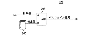
図2は、第1実施形態に係る判定回路126の構成の一例を示す。判定回路126は、判定値レジスタ200及び計数値比較器202を有する。判定値レジスタ200は、予め定められた判定値を格納し、計数値比較器202に供給する。例えば、判定値は、位相調整段階において論理比較器122により行われる比較回数の半値である。計数値比較器202は、フェイルカウンタ124が計数したフェイルデータの数である計数値をフェイルカウンタ124から取得し、判定値レジスタ200から供給された判定値と大小比較する。そして、計数値比較器202は、判定結果としてパスフェイル信号を出力し、位相調整制御回路128に供給する。例えば、計数値比較器202は、計数値が判定値より小さい場合にパスデータとして”1”を出力し、計数値が判定値以上の場合にフェイルデータとして”0”を出力する。なお、計数値比較器202は、計数値が判定値より小さい場合にフェイルデータとして”0”を出力し、計数値が判定値以上の場合にバスデータとして”1”を出力してしもよい。
FIG. 2 shows an example of the configuration of the
図3は、第1実施形態に係る位相調整制御回路128の構成の一例を示す。なお、図3では、可変遅延回路108、110、118の位相調整レジスタが4ビットの場合の例を説明する。なお、位相調整制御回路128は、可変遅延回路108、110、及び118のそれぞれに対応して、図3に示す構成要素をそれぞれ有する。また、本例においては、位相調整制御回路128をハードウェハ回路により実現する例を説明するが、ソフトウェアにより同様の機能を実現してもよい。
FIG. 3 shows an example of the configuration of the phase
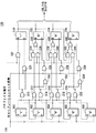
位相調整制御回路128は、ビット選択レジスタ300、302、304、306、及び308、論理積回路310、312、314、316、318、320、322、324、326、328、330、332、334、336、338、340、342、及び344、論理和回路350、352、354、356、358、及び360、並びに位相調整レジスタ370、372、374、及び376を有する。
The phase
ビット選択レジスタ300、302、304、306、及び308、並びに位相調整レジスタ370、372、374、及び376は、初期設定値を保持する。具体的には、ビット選択レジスタ300及び302は、”1”を保持する。また、ビット選択レジスタ304、306、及び308は、”0”を保持する。また、位相調整レジスタ370は、”1”を保持する。また、位相調整レジスタ372、374、及び306は、”0”を保持する。
The bit selection registers 300, 302, 304, 306, and 308 and the phase adjustment registers 370, 372, 374, and 376 hold initial setting values. Specifically, the bit selection registers 300 and 302 hold “1”. The bit selection registers 304, 306, and 308 hold “0”. The
ビット選択レジスタ300は、キャリブレーションセット信号に基づいて、保持しているビットデータを論理積回路310及び312、並びにビット選択レジスタ302に供給する。ビット選択レジスタ302は、キャリブレーションセット信号に基づいて、保持しているビットデータを論理積回路310、312、314、及び316、並びにビット選択レジスタ304に供給する。ビット選択レジスタ304は、キャリブレーションセット信号に基づいて、保持しているビットデータを論理積回路314、316、318、及び320、並びにビット選択レジスタ306に供給する。ビット選択レジスタ306は、キャリブレーションセット信号に基づいて、保持しているビットデータを論理積回路318、320、及び322、並びにビット選択レジスタ308に供給する。ビット選択レジスタ308は、キャリブレーションセット信号に基づいて、保持しているビットデータを論理積回路322、並びにビット選択レジスタ308に供給する。
The bit selection register 300 supplies the held bit data to the AND
ビット選択レジスタ300、302、304、306、及び308は、キャリブレーションセット信号が供給される毎に、保持しているビットデータを順にシフトさせて保持する。即ち、ビット選択レジスタ300、302、304、306、及び308は、初期設定において”1”、”1”、”0”、”0”、及び”0”をそれぞれ保持し、キャリブレーションセット信号が供給されると”0”、”1”、”1”、”0”、及び”0”をそれぞれ保持し、さらにキャリブレーションセット信号が供給されると”0”、”0”、”1”、”1”、及び”0”をそれぞれ保持し、さらにキャリブレーションセット信号が供給されると”0”、”0”、”0”、”1”、及び”1”をそれぞれ保持する。ビット選択レジスタ300、302、304、306、及び308が保持するビットデータをシフトさせることによって、位相調整レジスタ370、372、374、及び376を順に選択して設定値を決定する。 The bit selection registers 300, 302, 304, 306, and 308 sequentially shift and hold the held bit data every time the calibration set signal is supplied. That is, the bit selection registers 300, 302, 304, 306, and 308 respectively hold “1”, “1”, “0”, “0”, and “0” in the initial setting, and the calibration set signal is When supplied, it holds “0”, “1”, “1”, “0”, and “0”, respectively, and when a calibration set signal is supplied, it also holds “0”, “0”, “1”. , “1”, and “0” are held, and when a calibration set signal is supplied, “0”, “0”, “0”, “1”, and “1” are held. By shifting the bit data held in the bit selection registers 300, 302, 304, 306, and 308, the phase adjustment registers 370, 372, 374, and 376 are sequentially selected to determine the setting value.
論理積回路310は、ビット選択レジスタ300から供給されたビットデータと、ビット選択レジスタ302から出力されたビットデータとの論理積演算を行い、演算結果を論理積回路332及び論理積回路324に出力する。論理積回路312は、ビット選択レジスタ300から供給されたビットデータと、ビット選択レジスタ302から出力されたビットデータとの論理積演算を行い、演算結果を論理積回路334及び論理和回路350に出力する。論理積回路314は、ビット選択レジスタ302から供給されたビットデータと、ビット選択レジスタ304から出力されたビットデータとの論理積演算を行い、演算結果を論理積回路336及び論理和回路350に出力する。論理積回路316は、ビット選択レジスタ302から供給されたビットデータと、ビット選択レジスタ304から出力されたビットデータとの論理積演算を行い、演算結果を論理積回路338及び論理和回路352に出力する。
The AND
論理積回路318は、ビット選択レジスタ304から供給されたビットデータと、ビット選択レジスタ306から出力されたビットデータとの論理積演算を行い、演算結果を論理積回路340及び論理和回路352に出力する。論理積回路320は、ビット選択レジスタ304から供給されたビットデータと、ビット選択レジスタ306から出力されたビットデータとの論理積演算を行い、演算結果を論理積回路342及び論理和回路354に出力する。論理積回路322は、ビット選択レジスタ306から供給されたビットデータと、ビット選択レジスタ308から出力されたビットデータとの論理積演算を行い、演算結果を論理積回路344及び論理和回路354に出力する。
The AND
論理和回路350は、論理積回路312の出力と論理積回路314の出力との論理和演算を行い、演算結果を論理積回路326に出力する。論理和回路352は、論理積回路316の出力と論理積回路318の出力との論理和演算を行い、演算結果を論理積回路328に出力する。論理和回路354は、論理積回路320の出力と論理積回路322の出力との論理和演算を行い、演算結果を論理積回路330に出力する。
The
論理積回路324は、論理積回路310の出力とキャリブレーションセット信号との論理積演算を行い、演算結果を位相調整レジスタ370に出力する。論理積回路326は、論理和回路350の出力とキャリブレーションセット信号との論理積演算を行い、演算結果を位相調整レジスタ372に出力する。論理積回路328は、論理和回路352の出力とキャリブレーションセット信号との論理積演算を行い、演算結果を位相調整レジスタ374に出力する。論理積回路330は、論理和回路354の出力とキャリブレーションセット信号との論理積演算を行い、演算結果を位相調整レジスタ376に出力する。即ち、論理積回路324、326、328、及び330は、キャリブレーションセット信号が”1”にセットされている場合に、ビット選択レジスタ300、302、304、306、及び308によって選択されている位相調整レジスタ370、372、374、又は376にクロック信号を供給する。
The AND
論理積回路332は、判定回路126から供給されたパスフェイル信号と論理積回路310の出力との論理積演算を行い、演算結果を位相調整レジスタ370に出力する。そして、位相調整レジスタ370は、論理積回路324の出力に基づいて、保持しているビットデータを出力し、また論理積回路332の出力を保持する。
The AND
論理積回路334は、判定回路126から供給されたパスフェイル信号と位相調整レジスタ370が保持していたビットデータとの論理積演算を行い、演算結果を論理和回路356に出力する。論理積回路336は、判定回路126から供給されたパスフェイル信号と論理積回路314の出力との論理積演算を行い、演算結果を論理和回路356に出力する。論理和回路356は、論理積回路334の出力と論理積回路336の出力との論理和演算を行い、演算結果を位相調整レジスタ372に出力する。そして、位相調整レジスタ372は、論理積回路326の出力に基づいて、保持しているビットデータを出力し、また論理和回路356の出力を保持する。
The
論理積回路338は、判定回路126から供給されたパスフェイル信号と位相調整レジスタ372が保持していたビットデータとの論理積演算を行い、演算結果を論理和回路358に出力する。論理積回路340は、判定回路126から供給されたパスフェイル信号と論理積回路318の出力との論理積演算を行い、演算結果を論理和回路358に出力する。論理和回路358は、論理積回路338の出力と論理積回路340の出力との論理和演算を行い、演算結果を位相調整レジスタ374に出力する。そして、位相調整レジスタ374は、論理積回路328の出力に基づいて、保持しているビットデータを出力し、また論理和回路358の出力を保持する。
The
論理積回路342は、判定回路126から供給されたパスフェイル信号と位相調整レジスタ374が保持していたビットデータとの論理積演算を行い、演算結果を論理和回路360に出力する。論理積回路344は、判定回路126から供給されたパスフェイル信号と論理積回路322の出力との論理積演算を行い、演算結果を論理和回路360に出力する。論理和回路360は、論理積回路342の出力と論理積回路344の出力との論理和演算を行い、演算結果を位相調整レジスタ376に出力する。そして、位相調整レジスタ376は、論理積回路330の出力に基づいて、保持しているビットデータを出力し、また論理和回路358の出力を保持する。
The
以上のように位相調整段階において、位相調整レジスタ370、372、374、及び376は、判定回路126から供給されたパスフェイル信号及びキャリブレーションセット信号に基づいて、それぞれ1ビットの設定値を保持する。そして、被試験メモリ150の試験段階において、可変遅延回路108、110、又は118に設定値を供給することにより、可変遅延回路108、110、又は118によるストローブ信号の遅延量を調整する。
As described above, in the phase adjustment stage, the phase adjustment registers 370, 372, 374, and 376 each hold a 1-bit setting value based on the pass-fail signal and the calibration set signal supplied from the
図4は、第1実施形態に係る位相調整制御回路128の動作の一例を示す。図4では、図2に示した判定回路126、及び図3に示した位相調整制御回路128により可変遅延回路108及び110の遅延量を設定して、試験パターン信号の位相を調整する方法の一例を説明する。
FIG. 4 shows an example of the operation of the phase
まず、1回目の試験パターン信号を被試験メモリ150に印加しながら、論理比較器122が複数回に渡って出力値と期待値との比較を行い、フェイルカウンタ124がフェイルデータの数を計数する。そして、フェイルカウンタ124による計数値が判定値より小さい場合、即ちパスフェイル信号がパスデータとして”1”を出力する場合、位相調整制御回路128は、可変遅延回路108及び110の遅延量を増加させることにより試験パターン信号の位相を遅らせる。
First, while applying the first test pattern signal to the memory under
次に、2回目の試験パターン信号を被試験メモリ150に印加しながら、論理比較器122が複数回に渡って出力値と期待値との比較を行い、フェイルカウンタ124がフェイルデータの数を計数する。そして、フェイルカウンタ124による計数値が判定値より大きい場合、即ちパスフェイル信号がフェイルデータとして”0”を出力する場合、位相調整制御回路128は、可変遅延回路108及び110の遅延量を減少させることにより試験パターン信号の位相を進める。
Next, while applying the second test pattern signal to the memory under
次に、3回目の試験パターン信号を被試験メモリ150に印加しながら、論理比較器122が複数回に渡って出力値と期待値との比較を行い、フェイルカウンタ124がフェイルデータの数を計数する。そして、フェイルカウンタ124による計数値が判定値より小さい場合、即ちパスフェイル信号がバスデータとして”1”を出力する場合、位相調整制御回路128は、可変遅延回路108及び110の遅延量を増加させることにより試験パターン信号の位相を遅らせる。
Next, while applying the third test pattern signal to the memory under
次に、4回目の試験パターン信号を被試験メモリ150に印加しながら、論理比較器122が複数回に渡って出力値と期待値との比較を行い、フェイルカウンタ124がフェイルデータの数を計数する。そして、フェイルカウンタ124による計数値と、判定値レジスタ200が保持する判定値とがほぼ同じになり、位相調整制御回路128による位相調整が終了する。
Next, while applying the fourth test pattern signal to the memory under
即ち、本例においては、位相調整制御回路128は、2進数データで示される可変遅延回路108、110、又は118による遅延量を、判定回路126が出力した判定結果に基づいてバイナリサーチにより上位ビットから順に探索して決定していく。また、他の例においては、位相調整制御回路128は、シーケンシャルサーチによって可変遅延回路108、110、及び118の適切な遅延量を探索してもよいし、バイナリサーチとシーケンシャルサーチとの組み合わせによって可変遅延回路108、110、及び118の適切な遅延量を探索してもよい。
In other words, in this example, the phase
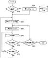
図5は、第1実施形態に係る試験方法のフローの一例を示す。本実施形態に係る位相調整は、被試験メモリ150を試験装置100のソケットに実装した状態で行い、被試験メモリ150のすべての端子について第1キャリブレーション(S502)による位相調整を行い、高速データ通信を行う端子については、第2キャリブレーション(S506)による位相調整を行う。
FIG. 5 shows an example of the flow of the test method according to the first embodiment. The phase adjustment according to the present embodiment is performed in a state where the memory under
まず、タイミング発生器102、電圧電流発生器、電圧電流測定器等を所定の状態に初期化するイニシャライズが実行されたか否かを判断する(S500)。イニシャライズが実行された場合には(S500−y)、試験条件毎に第1キャリブレーションを行う(S502)。第1キャリブレーション(S502)では、イニシャライズに発生した各端子に対する信号の位相のずれを可変遅延回路108及び110により調整するため、可変遅延回路108及び110の設定値をファイル化してキャリブレーションファイルとして保存する。イニシャライズが実行されなかった場合には(S500−n)、第1キャリブレーションを行わない。
First, it is determined whether or not initialization for initializing the
次に、試験条件に対応したキャリブレーションファイルを可変遅延回路108及び110の位相調整レジスタに転送して(S504)、第2キャリブレーションを行う(S506)。第2キャリブレーション(S506)では、被試験メモリ150の端子のうち、高速に動作する端子であるデータ入出力端子等に対してのみ位相調整が行われる。例えば、被試験メモリ150がXDRーDRAMである場合、RQ0−11、CFM/CFMN、RST、CMD、SCK、SDI、SDO等の端子に対しては第1キャリブレーション(S502)のみを行い、DQ/DQN0−15の端子に対して第1キャリブレーション(S502)に加え第2キャリブレーション(S506)を行う。
Next, the calibration file corresponding to the test condition is transferred to the phase adjustment registers of the
第2キャリブレーション(S506)が完了すると被試験メモリ150の試験を実行する(S508)。そして、同一の被試験メモリ150に対してさらに他の試験を実行するか否かを判断する(S510)。
When the second calibration (S506) is completed, the test of the memory under
同一の被試験メモリ150に対してさらに他の試験を実行する場合には(S510−y)、試験条件を変更するか否かを判断する(S512)。試験条件を変更しない場合には(S512−n)、続けて被試験メモリ150の試験を実行する(S508)。試験条件を変更する場合には(S512−y)、試験条件に対応したキャリブレーションファイルを可変遅延回路108及び110の位相調整レジスタに転送して(S504)、第2キャリブレーションを行う(S506)。
When still another test is executed on the same memory under test 150 (S510-y), it is determined whether or not the test condition is to be changed (S512). If the test conditions are not changed (S512-n), the test of the memory under
同一の被試験メモリ150に対してさらに他の試験を実行しない場合には(S510−n)、次の被試験メモリ150の試験を実行するか否かを判断する(S514)。次の被試験メモリ150の試験を実行する場合には(S514−y)、第2キャリブレーションを行う(S506)。そして、第2キャリブレーション(S506)が完了すると次の被試験メモリ150の試験を実行する(S508)。次の被試験メモリ150の試験を実行しない場合には(S514−n)、本試験フローを終了する。
When another test is not performed on the same memory under test 150 (S510-n), it is determined whether or not a test of the next memory under
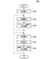
図6は、第1実施形態に係る位相調整方法のフローの一例を示す。図6では、第2キャリブレーション(S506)における位相調整方法のフローを説明する。まず、低速書込段階(S600)において、被試験メモリ150に試験パターン信号を低速で書き込む。低速書込段階(S600)では、シリアルバスを介して被試験メモリ150のスキャン入出力端子から試験パターン信号を書き込む。
FIG. 6 shows an example of the flow of the phase adjustment method according to the first embodiment. In FIG. 6, the flow of the phase adjustment method in the second calibration (S506) will be described. First, in the low-speed writing stage (S600), the test pattern signal is written into the memory under
次に、高速読出段階(S602)において、試験パターン信号に対応した出力信号を被試験メモリ150から高速で読み出す。高速読出段階(S602)では、被試験メモリ150のデータ入出力端子から試験パターン信号を読み出す。
Next, in the high-speed reading step (S602), the output signal corresponding to the test pattern signal is read from the memory under
次に、ストローブ信号位相調整段階(S604)において、タイミングコンパレータ120は、高速読出段階(S602)において被試験メモリ150から読み出された出力信号の出力値を、ストローブ信号のタイミングで取得する。そして、論理比較器122は、出力値を予め生成された期待値と比較して、比較結果を出力する。そして、図1から図4において説明したように、位相調整制御回路128は、論理比較器122の比較結果に基づいて、可変遅延回路118の位相調整用レジスタを設定し、タイミングコンパレータ120に供給されるストローブ信号のタイミングを調整することにより、タイミングコンパレータ120による出力信号のサンプリングのタイミングを調整する。
Next, in the strobe signal phase adjustment stage (S604), the
次に、高速書込段階(S606)において、SRラッチ112は、可変遅延回路108から供給されるセット信号のタイミングで試験パターン信号を立ち上げ、可変遅延回路110から供給されるリセット信号のタイミングで試験パターン信号を立ち下げて、試験パターン信号を被試験メモリ150に高速で書き込む。高速書込段階(S606)では、被試験メモリ150のデータ入出力端子から試験パターン信号を書き込む。
Next, in the high-speed writing stage (S606), the
次に、高速読出段階(S608)において、試験パターン信号に対応した出力信号を被試験メモリ150から高速で読み出す。高速読出段階(S608)では、被試験メモリ150のデータ入出力端子から試験パターン信号を読み出す。
Next, in a high-speed reading step (S608), an output signal corresponding to the test pattern signal is read from the memory under
次に、試験パターン信号位相調整段階(S610)において、タイミングコンパレータ120は、高速読出段階(S608)において被試験メモリ150から読み出された出力信号の出力値を、ストローブ信号のタイミングで取得する。そして、論理比較器122は、出力値を予め生成された期待値と比較して、比較結果を出力する。そして、図1から図4において説明したように、位相調整制御回路128は、論理比較器122の比較結果に基づいて、可変遅延回路108及び110の位相調整用レジスタを設定し、SRラッチ112に供給されるセット信号及びリセット信号のタイミングを調整することにより、被試験メモリ150に供給される試験パターン信号のタイミングを調整する。
Next, in the test pattern signal phase adjustment stage (S610), the
以上のように、低速書込段階(S600)において試験パターン信号を被試験メモリ150に低速で書き込み、試験パターン信号を被試験メモリ150に正確に保持させることによって、ストローブ信号位相調整段階(S604)においてタイミングコンパレータ120に供給されるストローブ信号の遅延量を精度よく設定することができる。また、ストローブ信号位相調整段階(S604)の後に試験パターン信号位相調整段階(S610)を実行することによって、試験パターン信号位相調整段階(S610)においてセット信号及びリセット信号の遅延量を精度よく設定することができる。
As described above, the test pattern signal is written into the memory under
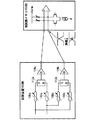
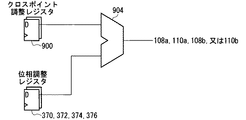
図7及び図8は、第1実施形態に係るドライバ114の一例を示す。また、図9は、第1実施形態に位相調整レジスタの構成の変形例を示す。ドライバ114は、差動ドライバであり、図7に示すように、被試験メモリ150の差動端子において差動信号が正しくクロスすること、また、差動信号の線路が等長であることが前提とされている。しかしながら、実際にはこのような前提に基づいて構成されることはなく、図8に示すように、シングルドライバ114a及び114bを用いて差動信号の位相を調整している。
7 and 8 show an example of the
即ち、試験装置100は、図8に示すように、可変遅延回路108及び110に換えて可変遅延回路108a、108b、110a、及び110bを備え、SRラッチ112に換えてSRラッチ112a及び112bを備え、ドライバ114に換えてドライバ114a及び114bを備える。また、試験装置100は、図9に示すように、位相調整レジスタ370、372、374、及び376に加え、クロスポイント調整レジスタ900、及び加算器904をさらに備える。
That is, the
SRラッチ112aは、可変遅延回路108aによって遅延されたセット信号により試験パターン信号を立ち上げ、可変遅延回路110aによって遅延されたリセット信号により試験パターン信号を立ち下げ、ドライバ114aを介して被試験メモリ150に供給する。また、SRラッチ112bは、可変遅延回路108bによって遅延されたセット信号により試験パターン信号を立ち上げ、可変遅延回路110bによって遅延されたリセット信号により試験パターン信号を立ち下げ、ドライバ114bを介して被試験メモリ150に供給する。
The
第1キャリブレーション(S502)において、被試験メモリ150の差動端子において差動信号のクロスポイントがハイレベルとロウレベルとの中心になるように調整する。そして、クロスポイント調整レジスタ900に調整した設定値を保持する。次に、第2キャリブレーション(S506)において、クロスポイントが中心からずれないように、可変遅延回路108a及び110bの位相を同時に調整し、また可変遅延回路108b及び110aの位相を同時に調整する。そして、位相調整レジスタ370、372、374、及び376に調整した設定値を保持する。次に、加算器904は、クロスポイント調整用レジスタ900に設定された設定値と、位相調整レジスタ370、372、374、及び376に設定された設定値とを加算して、可変遅延回路108a、110a、108b、又は110bに供給する。これにより、差動信号のクロスポイント調整と、試験パターン信号の位相調整とを同時に行うことができる。
In the first calibration (S502), adjustment is performed so that the cross point of the differential signal is at the center between the high level and the low level at the differential terminal of the memory under
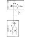
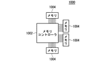
図10は、本発明の第2実施形態に係るメモリ制御システム1000の構成の一例を示す。メモリ制御システム1000は、メモリコントローラ1002、及び複数のメモリ1004を備える。メモリ制御システム1000は、データ転送を行う信号ラインに小振幅信号(200mV振幅)及び双方向差動インターフェースを最小し、複数のメモリ1004とメモリコントローラ1002との間を一対一接続する。また、メモリコントローラ1002のデータ入出力端子毎に、入力信号及び出力信号の位相調整機能が組み込まれている。
FIG. 10 shows an example of the configuration of a
図11は、第2実施形態に係るメモリコントローラ1002の構成の一例を示す。メモリコントローラ1002は、送受信制御部1100、温度検出部1130、リキャリブレーション制御部1132、及びリキャリブレーション間隔制御部1134を備える。送受信制御部1100は、ストローブ信号発生器1104、レベルコンパレータ1116、可変遅延回路1118、タイミングコンパレータ1120、論理比較器1122、フェイルカウンタ1124、判定回路1126、及び位相調整制御回路1128を有する。
FIG. 11 shows an example of the configuration of the
ストローブ信号発生器1104は、被試験メモリ150から出力された出力信号をタイミングコンパレータ1120がサンプリングするタイミングを指定するストローブ信号を発生する。可変遅延回路1118は、位相調整制御回路1128により予め設定された遅延量により、ストローブ信号発生器1104が発生したストローブ信号を遅延させてタイミングコンパレータ1120に供給する。また、レベルコンパレータ1116、可変遅延回路1118、タイミングコンパレータ1120、論理比較器1122、フェイルカウンタ1124、判定回路1126、及び位相調整制御回路1128のそれぞれは、図1に示した試験装置100が備えるレベルコンパレータ116、可変遅延回路118、タイミングコンパレータ120、論理比較器122、フェイルカウンタ124、判定回路126、及び位相調整制御回路128のそれぞれと同一の機能を有するので説明を省略する。また、メモリコントローラ1002は、図1に示した試験装置100が備えるその他の構成部材を備えてもよい。
The
温度検出部1130は、メモリ1004の温度又はメモリ1004の周囲の温度の変化を検出する。そして、リキャリブレーション制御部1132は、温度検出部1130が検出した温度変化が予め定められた温度変化以上である場合に、送受信制御部1100に対して、可変遅延回路1118による遅延量を再度設定することにより、タイミングコンパレータ1120に供給されるストローブ信号のタイミングを再度調整させる。即ち、メモリ1004の温度変化に起因して生じる出力信号の位相の変化に対して、ストローブ信号の位相を追従させることができる。そのため、メモリ1004が動作することによって温度が上昇する場合であっても、メモリ1004とメモリコントローラ1002との間のデータ通信を正確に行うことができる。
The
また、リキャリブレーション間隔制御部1134は、メモリ1004に対するデータの書き込み又は読み出しを連続して行った場合に、論理比較器1122が経過時間毎に出力した比較結果に基づいて、タイミングコンパレータ1120に供給されるストローブ信号のタイミングを再調整すべき時間間隔を測定する。具体的には、フェイルカウンタ1124は、論理比較器1122が出力したフェイルデータの数を単位時間毎に計数する。そして、判定回路1126は、予め定められた判定値と、フェイルカウンタ1124が計数した計数値とを大小比較する。これにより、リキャリブレーション間隔制御部1134は、計数値が判定値より大きくなる時間を測定する。即ち、メモリ1004に対するデータの書き込み又は読み出しを連続して行うことによって、メモリ1004の温度変化に起因して出力信号の位相の変化により、メモリコントローラ1002とメモリ1004との間のデータ通信が正確に行われなくなる時間を測定する。そして、リキャリブレーション間隔制御部1134は、測定した時間間隔毎に、送受信制御部1100に対して、タイミングコンパレータ1120に供給されるストローブ信号のタイミングを再調整させる。これにより、メモリ1004が動作することによって温度が上昇する場合であっても、常にメモリ1004とメモリコントローラ1002との間のデータ通信を正確に行うことができる。
In addition, the recalibration
なお、試験装置100は、図11に示したメモリコントローラ1002が備える温度検出部1130、リキャリブレーション制御部1132、及びリキャリブレーション間隔測定部1134をさらに備えてもよい。そして、被試験メモリ150の温度上昇に追従させてタイミングコンパレータ120に供給するストローブ信号のタイミングを調整してもよい。また、タイミングコンパレータ120に供給するストローブ信号のタイミングを再調整すべき時間間隔を測定して、メモリ1004に書き込んでもよい。メモリコントローラ1002は、試験装置100によって書き込まれた時間間隔にしたがってストローブ信号のタイミングを再調整することにより、常にメモリ1004とメモリコントローラ1002との間のデータ通信を正確に行うことができる。
Note that the
以上、実施形態を用いて本発明を説明したが、本発明の技術的範囲は上記実施形態に記載の範囲には限定されない。上記実施形態に、多様な変更又は改良を加えることができる。そのような変更又は改良を加えた形態も本発明の技術的範囲に含まれ得ることが、特許請求の範囲の記載から明らかである。 As mentioned above, although this invention was demonstrated using embodiment, the technical scope of this invention is not limited to the range as described in the said embodiment. Various modifications or improvements can be added to the above embodiment. It is apparent from the scope of the claims that the embodiments added with such changes or improvements can be included in the technical scope of the present invention.
100 試験装置
102 タイミング発生器
104 パターン発生器
106 波形整形器
108 可変遅延回路
110 可変遅延回路
112 SRラッチ
114 ドライバ
116 レベルコンパレータ
118 可変遅延回路
120 タイミングコンパレータ
122 論理比較器
124 フェイルカウンタ
126 判定回路
128 位相調整制御回路
200 判定値レジスタ
202 計数値比較器
900 クロスポイント調整レジスタ
904 加算器
1000 メモリ制御システム
1002 メモリコントローラ
1004 メモリ
1100 送受信制御部
1104 ストローブ信号発生器
1116 レベルコンパレータ
1118 可変遅延回路
1120 タイミングコンパレータ
1122 論理比較器
1124 フェイルカウンタ
1126 判定回路
1128 位相調整制御回路
1130 温度検出部
1132 リキャリブレーション制御部
1134 リキャリブレーション間隔制御部
DESCRIPTION OF
Claims (14)
前記被試験メモリから出力された出力信号の出力値を、ストローブ信号のタイミングで取得するタイミングコンパレータと、
前記タイミングコンパレータが取得した前記出力値を予め生成された期待値と比較して、比較結果を出力する論理比較器と、
前記論理比較器が出力した前記比較結果に基づいて、前記ストローブ信号のタイミングを調整する位相調整制御回路と
を備える試験装置。 A test apparatus for testing a memory under test,
A timing comparator for acquiring the output value of the output signal output from the memory under test at the timing of the strobe signal;
A logical comparator that compares the output value acquired by the timing comparator with an expected value generated in advance and outputs a comparison result;
A test apparatus comprising: a phase adjustment control circuit that adjusts a timing of the strobe signal based on the comparison result output from the logical comparator.
をさらに備え、
前記位相調整制御回路は、前記論理比較器が出力した前記比較結果に基づいて、前記第1可変遅延回路による遅延量を設定する
請求項1に記載の試験装置。 A first variable delay circuit for delaying the strobe signal and supplying the delayed signal to the timing comparator;
The test apparatus according to claim 1, wherein the phase adjustment control circuit sets a delay amount by the first variable delay circuit based on the comparison result output from the logical comparator.
前記フェイルカウンタが計数した前記フェイルデータの数を、予め定められた判定値と比較して、判定結果を出力する判定回路と
をさらに備え、
前記位相調整制御回路は、前記判定回路が出力した前記判定結果に基づいて、前記第1可変遅延回路による遅延量を設定する
請求項2に記載の試験装置。 A fail counter that counts the number of fail data that the logical comparator outputs as the comparison result and indicates that the output value does not match the expected value;
A determination circuit that compares the number of the fail data counted by the fail counter with a predetermined determination value and outputs a determination result;
The test apparatus according to claim 2, wherein the phase adjustment control circuit sets a delay amount by the first variable delay circuit based on the determination result output from the determination circuit.
請求項3に記載の試験装置。 The phase adjustment control circuit determines the delay amount by the first variable delay circuit indicated by binary data in order from the upper bit by a binary search based on the determination result output from the determination circuit. 3. The test apparatus according to 3.
前記セット信号を遅延させて前記SRラッチに供給する第2可変遅延回路と、
前記リセット信号を遅延させて前記SRラッチに供給する第3可変遅延回路と
をさらに備え、
前記タイミングコンパレータは、前記試験パターン信号に対応して前記被試験メモリから出力された出力信号の出力値を、前記被試験メモリの内部クロックと同期した前記ストローブ信号のタイミングで取得し、
前記論理比較器は、前記タイミングコンパレータが取得した前記出力値を前記期待値と比較して、比較結果を出力し、
前記位相調整制御回路は、前記論理比較器が出力した前記比較結果に基づいて、前記第2可変遅延回路及び前記3可変遅延回路による遅延量を設定する
請求項1に記載の試験装置。 An SR latch that raises the test pattern signal at the timing of the set signal, lowers the test pattern signal at the timing of the reset signal, and supplies the test pattern signal to the memory under test;
A second variable delay circuit that delays the set signal and supplies the set signal to the SR latch;
A third variable delay circuit that delays the reset signal and supplies the delayed signal to the SR latch;
The timing comparator acquires an output value of an output signal output from the memory under test corresponding to the test pattern signal at a timing of the strobe signal synchronized with an internal clock of the memory under test,
The logical comparator compares the output value acquired by the timing comparator with the expected value, and outputs a comparison result,
The test apparatus according to claim 1, wherein the phase adjustment control circuit sets a delay amount by the second variable delay circuit and the three variable delay circuit based on the comparison result output by the logical comparator.
前記温度検出部が検出した温度変化が予め定められた温度変化以上である場合に、前記ストローブ信号のタイミングを再度調整させるリキャリブレーション制御部と
をさらに備える請求項1に記載の試験装置。 A temperature detector for detecting a change in the temperature of the memory under test or the temperature around the memory under test;
The test apparatus according to claim 1, further comprising: a recalibration control unit that adjusts the timing of the strobe signal again when the temperature change detected by the temperature detection unit is equal to or greater than a predetermined temperature change.
をさらに備える請求項1に記載の試験装置。 Based on the comparison result output by the logical comparator at every elapsed time when data is continuously written to or read from the memory under test, a time interval at which the timing of the strobe signal should be readjusted is determined. The test apparatus according to claim 1, further comprising a recalibration interval control unit for measuring.
前記被試験メモリから出力された前記出力信号の出力値を、前記ストローブ信号のタイミングで取得する出力値取得段階と、
取得された前記出力値を予め生成された期待値と比較して、比較結果を出力する段階と、
前記比較結果に基づいて、前記ストローブ信号のタイミングを調整する段階と
を備える位相調整方法。 A phase adjustment method for adjusting the timing of an output signal and a strobe signal output from a memory under test,
An output value acquisition step of acquiring the output value of the output signal output from the memory under test at the timing of the strobe signal;
Comparing the acquired output value with an expected value generated in advance, and outputting a comparison result;
Adjusting the timing of the strobe signal based on the comparison result.
前記試験パターン信号に対応した前記出力信号を前記被試験メモリから高速で読み出す第1高速読出段階と
をさらに備え、
前記出力値取得段階は、前記第1高速読出段階において読み出された前記出力信号の前記出力値を、前記ストローブ信号のタイミングで取得する段階を有する
請求項8に記載の位相調整方法。 A low-speed writing step of writing a test pattern signal to the memory under test at a low speed;
A first high-speed reading step of reading the output signal corresponding to the test pattern signal from the memory under test at high speed;
The phase adjustment method according to claim 8, wherein the output value acquisition step includes a step of acquiring the output value of the output signal read in the first high-speed reading step at a timing of the strobe signal.
前記第1高速読出段階は、前記被試験メモリのデータ入出力端子から前記試験パターン信号を読み出す段階を有する
請求項9に記載の位相調整方法。 The low-speed writing step includes writing the test pattern signal from a scan input / output terminal of the memory under test;
10. The phase adjustment method according to claim 9, wherein the first high-speed reading step includes a step of reading the test pattern signal from a data input / output terminal of the memory under test.
前記試験パターン信号に対応した前記出力信号を前記被試験メモリから高速で読み出す第2高速読出段階と、
前記第2高速読出段階において読み出された前記出力信号の出力値を、前記ストローブ信号のタイミングで取得する段階と、
取得された前記出力値を予め生成された前記期待値と比較して、比較結果を出力する段階と、
前記比較結果に基づいて、前記セット信号及び前記リセット信号のタイミングを調整する段階と
をさらに備える請求項8に記載の位相調整方法。 A high-speed writing step of rising the test pattern signal at the timing of the set signal, lowering the test pattern signal at the timing of the reset signal, and writing the test pattern signal to the memory under test at high speed;
A second high-speed reading step of reading the output signal corresponding to the test pattern signal from the memory under test at a high speed;
Obtaining an output value of the output signal read in the second high-speed reading step at a timing of the strobe signal;
Comparing the acquired output value with the expected value generated in advance, and outputting a comparison result;
The phase adjustment method according to claim 8, further comprising: adjusting timings of the set signal and the reset signal based on the comparison result.
前記第2高速読出段階は、前記被試験メモリのデータ入出力端子から前記試験パターン信号を読み出す段階を有する
請求項11に記載の位相調整方法。 The high-speed writing step includes a step of writing the test pattern signal from a data input / output terminal of the memory under test.
12. The phase adjustment method according to claim 11, wherein the second high-speed reading step includes a step of reading the test pattern signal from a data input / output terminal of the memory under test.
前記メモリから読み出された出力信号の出力値を、ストローブ信号のタイミングで取得するタイミングコンパレータと、
前記タイミングコンパレータが取得した前記出力値を予め生成された期待値と比較して、比較結果を出力する論理比較器と、
前記論理比較器が出力した前記比較結果に基づいて、前記ストローブ信号のタイミングを調整する位相調整制御回路と、
前記メモリの温度又は前記メモリの周囲の温度の変化を検出する温度検出部と、
前記温度検出部が検出した温度変化が予め定められた温度変化以上である場合に、前記ストローブ信号のタイミングを再度調整させるリキャリブレーション制御部と
を備えるメモリコントローラ。 A memory controller that controls writing and reading of data in a memory,
A timing comparator that obtains the output value of the output signal read from the memory at the timing of the strobe signal;
A logical comparator that compares the output value acquired by the timing comparator with an expected value generated in advance and outputs a comparison result;
A phase adjustment control circuit that adjusts the timing of the strobe signal based on the comparison result output by the logical comparator;
A temperature detector for detecting a change in the temperature of the memory or the temperature around the memory;
A memory controller comprising: a recalibration control unit that adjusts the timing of the strobe signal again when the temperature change detected by the temperature detection unit is equal to or greater than a predetermined temperature change.
前記メモリから読み出された出力信号の出力値を、ストローブ信号のタイミングで取得するタイミングコンパレータと、
前記タイミングコンパレータが取得した前記出力値を予め生成された期待値と比較して、比較結果を出力する論理比較器と、
前記論理比較器が出力した前記比較結果に基づいて、前記ストローブ信号のタイミングを調整する位相調整制御回路と、
前記メモリに対するデータの書き込み又は読み出しを連続して行った場合に、前記論理比較器が経過時間毎に出力した前記比較結果に基づいて、前記ストローブ信号のタイミングを再調整すべき時間間隔を測定するリキャリブレーション間隔制御部と
を備えるメモリコントローラ。 A memory controller that controls writing and reading of data in a memory,
A timing comparator that obtains the output value of the output signal read from the memory at the timing of the strobe signal;
A logical comparator that compares the output value acquired by the timing comparator with an expected value generated in advance and outputs a comparison result;
A phase adjustment control circuit that adjusts the timing of the strobe signal based on the comparison result output by the logical comparator;
When writing or reading data to or from the memory continuously, a time interval at which the timing of the strobe signal should be readjusted is measured based on the comparison result output by the logical comparator every elapsed time. A memory controller comprising a recalibration interval control unit.
Priority Applications (6)
| Application Number | Priority Date | Filing Date | Title |
|---|---|---|---|
| JP2004111494A JP4451189B2 (en) | 2004-04-05 | 2004-04-05 | Test apparatus, phase adjustment method, and memory controller |
| KR1020067023285A KR100840800B1 (en) | 2004-04-05 | 2005-03-25 | Test device, phase adjustment method, and memory controller |
| CNB2005800101694A CN100505107C (en) | 2004-04-05 | 2005-03-25 | Test device, phase adjustment method and memory controller |
| DE112005000745T DE112005000745T5 (en) | 2004-04-05 | 2005-03-25 | Test device, phase adjustment and memory control |
| PCT/JP2005/005547 WO2005098868A1 (en) | 2004-04-05 | 2005-03-25 | Test apparatus, phase adjusting method and memory controller |
| US11/180,895 US7266738B2 (en) | 2004-04-05 | 2005-07-13 | Test apparatus, phase adjusting method and memory controller |
Applications Claiming Priority (1)
| Application Number | Priority Date | Filing Date | Title |
|---|---|---|---|
| JP2004111494A JP4451189B2 (en) | 2004-04-05 | 2004-04-05 | Test apparatus, phase adjustment method, and memory controller |
Publications (3)
| Publication Number | Publication Date |
|---|---|
| JP2005293808A true JP2005293808A (en) | 2005-10-20 |
| JP2005293808A5 JP2005293808A5 (en) | 2008-08-21 |
| JP4451189B2 JP4451189B2 (en) | 2010-04-14 |
Family
ID=35125332
Family Applications (1)
| Application Number | Title | Priority Date | Filing Date |
|---|---|---|---|
| JP2004111494A Expired - Fee Related JP4451189B2 (en) | 2004-04-05 | 2004-04-05 | Test apparatus, phase adjustment method, and memory controller |
Country Status (6)
| Country | Link |
|---|---|
| US (1) | US7266738B2 (en) |
| JP (1) | JP4451189B2 (en) |
| KR (1) | KR100840800B1 (en) |
| CN (1) | CN100505107C (en) |
| DE (1) | DE112005000745T5 (en) |
| WO (1) | WO2005098868A1 (en) |
Cited By (7)
| Publication number | Priority date | Publication date | Assignee | Title |
|---|---|---|---|---|
| JP2009032310A (en) * | 2007-07-25 | 2009-02-12 | Fujitsu Ltd | High speed product testing method and equipment |
| WO2010023924A1 (en) * | 2008-08-28 | 2010-03-04 | 株式会社アドバンテスト | Interconnect circuit board, skew measuring method and testing device |
| WO2010058441A1 (en) * | 2008-11-19 | 2010-05-27 | 株式会社アドバンテスト | Test equipment, test method, and program |
| JP2011060392A (en) * | 2009-09-11 | 2011-03-24 | Nec Corp | Method for testing semiconductor memory device |
| CN104764914A (en) * | 2014-01-03 | 2015-07-08 | 致茂电子股份有限公司 | Error Compensation Method and Automatic Test Equipment Using the Method |
| JP2015532488A (en) * | 2012-10-05 | 2015-11-09 | クアルコム,インコーポレイテッド | Algorithm for optimal use of external memory tuning sequences |
| JP2017122718A (en) * | 2015-12-09 | 2017-07-13 | 致茂電子股▲分▼有限公司Chroma Ate Inc. | Pulse generator and pulse generator calibration method |
Families Citing this family (30)
| Publication number | Priority date | Publication date | Assignee | Title |
|---|---|---|---|---|
| US7254763B2 (en) * | 2004-09-01 | 2007-08-07 | Agere Systems Inc. | Built-in self test for memory arrays using error correction coding |
| KR100639678B1 (en) * | 2004-11-16 | 2006-10-30 | 삼성전자주식회사 | test device |
| US7573957B2 (en) * | 2005-09-23 | 2009-08-11 | Teradyne, Inc. | Strobe technique for recovering a clock in a digital signal |
| US7856578B2 (en) * | 2005-09-23 | 2010-12-21 | Teradyne, Inc. | Strobe technique for test of digital signal timing |
| US7574632B2 (en) * | 2005-09-23 | 2009-08-11 | Teradyne, Inc. | Strobe technique for time stamping a digital signal |
| JP4949707B2 (en) * | 2006-03-22 | 2012-06-13 | ルネサスエレクトロニクス株式会社 | Semiconductor device and test method thereof |
| US7603246B2 (en) * | 2006-03-31 | 2009-10-13 | Nvidia Corporation | Data interface calibration |
| US7715251B2 (en) * | 2006-10-25 | 2010-05-11 | Hewlett-Packard Development Company, L.P. | Memory access strobe configuration system and process |
| US7797121B2 (en) * | 2007-06-07 | 2010-09-14 | Advantest Corporation | Test apparatus, and device for calibration |
| WO2009025020A1 (en) * | 2007-08-20 | 2009-02-26 | Advantest Corporation | Tester, test method, and manufacturing method |
| US8521979B2 (en) | 2008-05-29 | 2013-08-27 | Micron Technology, Inc. | Memory systems and methods for controlling the timing of receiving read data |
| US8289760B2 (en) | 2008-07-02 | 2012-10-16 | Micron Technology, Inc. | Multi-mode memory device and method having stacked memory dice, a logic die and a command processing circuit and operating in direct and indirect modes |
| US7855931B2 (en) | 2008-07-21 | 2010-12-21 | Micron Technology, Inc. | Memory system and method using stacked memory device dice, and system using the memory system |
| US8756486B2 (en) | 2008-07-02 | 2014-06-17 | Micron Technology, Inc. | Method and apparatus for repairing high capacity/high bandwidth memory devices |
| US7808849B2 (en) * | 2008-07-08 | 2010-10-05 | Nvidia Corporation | Read leveling of memory units designed to receive access requests in a sequential chained topology |
| JP5171442B2 (en) * | 2008-07-08 | 2013-03-27 | 株式会社アドバンテスト | Multi-strobe circuit and test equipment |
| US7796465B2 (en) * | 2008-07-09 | 2010-09-14 | Nvidia Corporation | Write leveling of memory units designed to receive access requests in a sequential chained topology |
| US8461884B2 (en) * | 2008-08-12 | 2013-06-11 | Nvidia Corporation | Programmable delay circuit providing for a wide span of delays |
| US8274272B2 (en) * | 2009-02-06 | 2012-09-25 | Advanced Micro Devices, Inc. | Programmable delay module testing device and methods thereof |
| JP5477062B2 (en) * | 2010-03-08 | 2014-04-23 | 富士通セミコンダクター株式会社 | Semiconductor integrated circuit test apparatus, test method, and program |
| US8400808B2 (en) | 2010-12-16 | 2013-03-19 | Micron Technology, Inc. | Phase interpolators and push-pull buffers |
| US8612815B2 (en) * | 2011-12-16 | 2013-12-17 | International Business Machines Corporation | Asynchronous circuit with an at-speed built-in self-test (BIST) architecture |
| US9171597B2 (en) | 2013-08-30 | 2015-10-27 | Micron Technology, Inc. | Apparatuses and methods for providing strobe signals to memories |
| CN104616697A (en) * | 2014-12-17 | 2015-05-13 | 曙光信息产业(北京)有限公司 | QDR-SRAM (Quad data rate-static random access memory) clock phase adjusting method and device |
| US10867642B2 (en) | 2016-05-17 | 2020-12-15 | Taiwan Semiconductor Manufacturing Company Limited | Active random access memory |
| CN114062889B (en) * | 2020-08-04 | 2024-08-27 | 瑞昱半导体股份有限公司 | Device for detecting allowance of circuit operation speed |
| CN113868107B (en) * | 2021-09-10 | 2024-04-26 | 长沙市致存科技有限责任公司 | Self-adaptive adjustment method, device, equipment and medium for back-end IO of storage product |
| US11726904B2 (en) | 2021-09-23 | 2023-08-15 | International Business Machines Corporation | Controlled input/output in progress state during testcase processing |
| CN114116581A (en) * | 2021-10-14 | 2022-03-01 | 北京国科天迅科技有限公司 | Method and device for improving high-speed serial bus burst transmission response performance |
| KR20240056205A (en) * | 2022-10-21 | 2024-04-30 | 매그나칩믹스드시그널 유한회사 | Memory repair device |
Family Cites Families (12)
| Publication number | Priority date | Publication date | Assignee | Title |
|---|---|---|---|---|
| JP3636506B2 (en) * | 1995-06-19 | 2005-04-06 | 株式会社アドバンテスト | Semiconductor test equipment |
| JP3607325B2 (en) * | 1994-09-22 | 2005-01-05 | 株式会社アドバンテスト | Comparison circuit for semiconductor test equipment |
| US5732047A (en) * | 1995-12-12 | 1998-03-24 | Advantest Corporation | Timing comparator circuit for use in device testing apparatus |
| JPH09166646A (en) * | 1995-12-15 | 1997-06-24 | Nec Corp | Semiconductor device |
| TW343282B (en) * | 1996-06-14 | 1998-10-21 | Adoban Tesuto Kk | Testing device for a semiconductor device |
| JP3718374B2 (en) * | 1999-06-22 | 2005-11-24 | 株式会社東芝 | Memory-embedded semiconductor integrated circuit device and test method thereof |
| JP3453133B2 (en) * | 1999-08-16 | 2003-10-06 | 株式会社アドバンテスト | Timing calibration method for IC test apparatus and IC test apparatus having calibration function using the calibration method |
| JP2001222897A (en) * | 2000-02-04 | 2001-08-17 | Advantest Corp | Semiconductor test device |
| JP4291494B2 (en) * | 2000-04-04 | 2009-07-08 | 株式会社アドバンテスト | IC test equipment timing calibration equipment |
| US6377065B1 (en) * | 2000-04-13 | 2002-04-23 | Advantest Corp. | Glitch detection for semiconductor test system |
| JP2002181899A (en) * | 2000-12-15 | 2002-06-26 | Advantest Corp | Method of calibrating timing |
| JP2003098235A (en) * | 2001-09-27 | 2003-04-03 | Matsushita Electric Ind Co Ltd | Semiconductor integrated circuit and inspection method thereof |
-
2004
- 2004-04-05 JP JP2004111494A patent/JP4451189B2/en not_active Expired - Fee Related
-
2005
- 2005-03-25 DE DE112005000745T patent/DE112005000745T5/en not_active Withdrawn
- 2005-03-25 CN CNB2005800101694A patent/CN100505107C/en not_active Expired - Fee Related
- 2005-03-25 WO PCT/JP2005/005547 patent/WO2005098868A1/en not_active Ceased
- 2005-03-25 KR KR1020067023285A patent/KR100840800B1/en not_active Expired - Fee Related
- 2005-07-13 US US11/180,895 patent/US7266738B2/en not_active Expired - Lifetime
Cited By (12)
| Publication number | Priority date | Publication date | Assignee | Title |
|---|---|---|---|---|
| JP2009032310A (en) * | 2007-07-25 | 2009-02-12 | Fujitsu Ltd | High speed product testing method and equipment |
| WO2010023924A1 (en) * | 2008-08-28 | 2010-03-04 | 株式会社アドバンテスト | Interconnect circuit board, skew measuring method and testing device |
| US7768255B2 (en) | 2008-08-28 | 2010-08-03 | Advantest Corporation | Interconnection substrate, skew measurement method, and test apparatus |
| KR101178069B1 (en) | 2008-08-28 | 2012-08-30 | 가부시키가이샤 어드밴티스트 | Interconnect circuit board, skew measuring method and testing device |
| JP5475666B2 (en) * | 2008-08-28 | 2014-04-16 | 株式会社アドバンテスト | Skew measuring method and test apparatus |
| WO2010058441A1 (en) * | 2008-11-19 | 2010-05-27 | 株式会社アドバンテスト | Test equipment, test method, and program |
| JPWO2010058441A1 (en) * | 2008-11-19 | 2012-04-12 | 株式会社アドバンテスト | Test apparatus, test method, and program |
| JP2011060392A (en) * | 2009-09-11 | 2011-03-24 | Nec Corp | Method for testing semiconductor memory device |
| JP2015532488A (en) * | 2012-10-05 | 2015-11-09 | クアルコム,インコーポレイテッド | Algorithm for optimal use of external memory tuning sequences |
| JP2018125040A (en) * | 2012-10-05 | 2018-08-09 | クアルコム,インコーポレイテッド | Algorithm for optimal usage of external memory tuning sequence |
| CN104764914A (en) * | 2014-01-03 | 2015-07-08 | 致茂电子股份有限公司 | Error Compensation Method and Automatic Test Equipment Using the Method |
| JP2017122718A (en) * | 2015-12-09 | 2017-07-13 | 致茂電子股▲分▼有限公司Chroma Ate Inc. | Pulse generator and pulse generator calibration method |
Also Published As
| Publication number | Publication date |
|---|---|
| KR20070001264A (en) | 2007-01-03 |
| CN1938788A (en) | 2007-03-28 |
| CN100505107C (en) | 2009-06-24 |
| US7266738B2 (en) | 2007-09-04 |
| DE112005000745T5 (en) | 2007-02-22 |
| KR100840800B1 (en) | 2008-06-23 |
| US20060041799A1 (en) | 2006-02-23 |
| JP4451189B2 (en) | 2010-04-14 |
| WO2005098868A1 (en) | 2005-10-20 |
Similar Documents
| Publication | Publication Date | Title |
|---|---|---|
| JP4451189B2 (en) | Test apparatus, phase adjustment method, and memory controller | |
| JP3920318B1 (en) | Test apparatus and test method | |
| JP5613666B2 (en) | Tracking circuit and method for automatic test equipment system | |
| JP4878215B2 (en) | Interface circuit and memory control device | |
| US7619404B2 (en) | System and method for testing integrated circuit timing margins | |
| US7644324B2 (en) | Semiconductor memory tester | |
| US7078889B2 (en) | Semiconductor test apparatus for testing semiconductor device that produces output data by its internal clock timing | |
| US7222273B2 (en) | Apparatus and method for testing semiconductor memory devices, capable of selectively changing frequencies of test pattern signals | |
| US20100182857A1 (en) | Tester for semiconductor device and semiconductor device | |
| JP5254794B2 (en) | Strobe technique for testing the timing of digital signals | |
| JP2008145361A (en) | Semiconductor device | |
| JPWO2005012930A1 (en) | Test equipment | |
| US7135880B2 (en) | Test apparatus | |
| US7206985B2 (en) | Method and apparatus for calibrating a test system for an integrated semiconductor circuit | |
| US10002650B1 (en) | Signal quality detection circuit for generating signal quality detection result according to two-dimensional nominal sampling point pattern and associated signal quality detection method | |
| JPWO2007072738A1 (en) | Test apparatus, adjustment apparatus, adjustment method, and adjustment program | |
| JP4320733B2 (en) | Semiconductor test equipment | |
| JP2009047480A (en) | Semiconductor test equipment | |
| JP2006105636A (en) | Semiconductor-testing device and its calibration method | |
| JP5249357B2 (en) | Electronic device, test apparatus and test method | |
| JPWO2010087009A1 (en) | Electronic device, test apparatus and test method | |
| JPWO2007129491A1 (en) | Test equipment, circuits and electronic devices |
Legal Events
| Date | Code | Title | Description |
|---|---|---|---|
| A621 | Written request for application examination |
Free format text: JAPANESE INTERMEDIATE CODE: A621 Effective date: 20070105 |
|
| A521 | Request for written amendment filed |
Free format text: JAPANESE INTERMEDIATE CODE: A523 Effective date: 20070518 |
|
| A131 | Notification of reasons for refusal |
Free format text: JAPANESE INTERMEDIATE CODE: A131 Effective date: 20090714 |
|
| A521 | Request for written amendment filed |
Free format text: JAPANESE INTERMEDIATE CODE: A523 Effective date: 20090908 |
|
| TRDD | Decision of grant or rejection written | ||
| A01 | Written decision to grant a patent or to grant a registration (utility model) |
Free format text: JAPANESE INTERMEDIATE CODE: A01 Effective date: 20100119 |
|
| A01 | Written decision to grant a patent or to grant a registration (utility model) |
Free format text: JAPANESE INTERMEDIATE CODE: A01 |
|
| A61 | First payment of annual fees (during grant procedure) |
Free format text: JAPANESE INTERMEDIATE CODE: A61 Effective date: 20100127 |
|
| R150 | Certificate of patent or registration of utility model |
Free format text: JAPANESE INTERMEDIATE CODE: R150 |
|
| FPAY | Renewal fee payment (event date is renewal date of database) |
Free format text: PAYMENT UNTIL: 20130205 Year of fee payment: 3 |
|
| FPAY | Renewal fee payment (event date is renewal date of database) |
Free format text: PAYMENT UNTIL: 20130205 Year of fee payment: 3 |
|
| FPAY | Renewal fee payment (event date is renewal date of database) |
Free format text: PAYMENT UNTIL: 20130205 Year of fee payment: 3 |
|
| R250 | Receipt of annual fees |
Free format text: JAPANESE INTERMEDIATE CODE: R250 |
|
| LAPS | Cancellation because of no payment of annual fees |