EP3989240A1 - Imaging type x-ray microscope - Google Patents
Imaging type x-ray microscope Download PDFInfo
- Publication number
- EP3989240A1 EP3989240A1 EP21203333.6A EP21203333A EP3989240A1 EP 3989240 A1 EP3989240 A1 EP 3989240A1 EP 21203333 A EP21203333 A EP 21203333A EP 3989240 A1 EP3989240 A1 EP 3989240A1
- Authority
- EP
- European Patent Office
- Prior art keywords
- ray
- imaging
- mirror
- rays
- type
- Prior art date
- Legal status (The legal status is an assumption and is not a legal conclusion. Google has not performed a legal analysis and makes no representation as to the accuracy of the status listed.)
- Pending
Links
Images




Classifications
-
- G—PHYSICS
- G21—NUCLEAR PHYSICS; NUCLEAR ENGINEERING
- G21K—HANDLING OF PARTICLES OR IONISING RADIATION NOT OTHERWISE PROVIDED FOR; IRRADIATION DEVICES; GAMMA RAY OR X-RAY MICROSCOPES
- G21K7/00—Gamma- or X-ray microscopes
-
- G—PHYSICS
- G01—MEASURING; TESTING
- G01N—INVESTIGATING OR ANALYSING MATERIALS BY DETERMINING THEIR CHEMICAL OR PHYSICAL PROPERTIES
- G01N23/00—Investigating or analysing materials by the use of wave or particle radiation, e.g. X-rays or neutrons, not covered by groups G01N3/00 – G01N17/00, G01N21/00 or G01N22/00
- G01N23/02—Investigating or analysing materials by the use of wave or particle radiation, e.g. X-rays or neutrons, not covered by groups G01N3/00 – G01N17/00, G01N21/00 or G01N22/00 by transmitting the radiation through the material
- G01N23/04—Investigating or analysing materials by the use of wave or particle radiation, e.g. X-rays or neutrons, not covered by groups G01N3/00 – G01N17/00, G01N21/00 or G01N22/00 by transmitting the radiation through the material and forming images of the material
-
- G—PHYSICS
- G01—MEASURING; TESTING
- G01N—INVESTIGATING OR ANALYSING MATERIALS BY DETERMINING THEIR CHEMICAL OR PHYSICAL PROPERTIES
- G01N23/00—Investigating or analysing materials by the use of wave or particle radiation, e.g. X-rays or neutrons, not covered by groups G01N3/00 – G01N17/00, G01N21/00 or G01N22/00
- G01N23/02—Investigating or analysing materials by the use of wave or particle radiation, e.g. X-rays or neutrons, not covered by groups G01N3/00 – G01N17/00, G01N21/00 or G01N22/00 by transmitting the radiation through the material
- G01N23/04—Investigating or analysing materials by the use of wave or particle radiation, e.g. X-rays or neutrons, not covered by groups G01N3/00 – G01N17/00, G01N21/00 or G01N22/00 by transmitting the radiation through the material and forming images of the material
- G01N23/046—Investigating or analysing materials by the use of wave or particle radiation, e.g. X-rays or neutrons, not covered by groups G01N3/00 – G01N17/00, G01N21/00 or G01N22/00 by transmitting the radiation through the material and forming images of the material using tomography, e.g. computed tomography [CT]
-
- G—PHYSICS
- G21—NUCLEAR PHYSICS; NUCLEAR ENGINEERING
- G21K—HANDLING OF PARTICLES OR IONISING RADIATION NOT OTHERWISE PROVIDED FOR; IRRADIATION DEVICES; GAMMA RAY OR X-RAY MICROSCOPES
- G21K1/00—Arrangements for handling particles or ionising radiation, e.g. focusing or moderating
- G21K1/06—Arrangements for handling particles or ionising radiation, e.g. focusing or moderating using diffraction, refraction or reflection, e.g. monochromators
- G21K1/062—Devices having a multilayer structure
-
- G—PHYSICS
- G01—MEASURING; TESTING
- G01N—INVESTIGATING OR ANALYSING MATERIALS BY DETERMINING THEIR CHEMICAL OR PHYSICAL PROPERTIES
- G01N2223/00—Investigating materials by wave or particle radiation
- G01N2223/03—Investigating materials by wave or particle radiation by transmission
-
- G—PHYSICS
- G01—MEASURING; TESTING
- G01N—INVESTIGATING OR ANALYSING MATERIALS BY DETERMINING THEIR CHEMICAL OR PHYSICAL PROPERTIES
- G01N2223/00—Investigating materials by wave or particle radiation
- G01N2223/10—Different kinds of radiation or particles
- G01N2223/101—Different kinds of radiation or particles electromagnetic radiation
- G01N2223/1016—X-ray
-
- G—PHYSICS
- G01—MEASURING; TESTING
- G01N—INVESTIGATING OR ANALYSING MATERIALS BY DETERMINING THEIR CHEMICAL OR PHYSICAL PROPERTIES
- G01N2223/00—Investigating materials by wave or particle radiation
- G01N2223/30—Accessories, mechanical or electrical features
Definitions
- the present invention relates to a technique for greatly improving the performance of an imaging type X-ray microscope in a laboratory.
- a Fresnel zone plate lens (FZP) is often used for an imaging system (for example, see Patent Document 1).
- FZP Fresnel zone plate lens
- the efficiency becomes several percent or less.
- NA numerical aperture
- NA is 1 mrad or less, which is very low. Therefore, it has been difficult to realize a high-resolution X-ray microscope using high-energy X-rays in a laboratory.
- an X-ray microscope using a Kirkpatrick-Baez mirror (KB mirror) with a size enable to be carried into a room has been developed (e.g., see Patent Document 2).
- an imaging system is configured using a KB mirror having a reflection concave surface and a KB mirror having a reflection convex surface. As a result, the rear focal length of the optical system is shortened while the magnification is maintained.
- the present invention has been made in view of the above circumstances, and an object thereof is to provide an imaging type X-ray microscope capable of enlarging the numerical aperture even with high energy X-rays, and capable of acquiring an enlarged image with sufficient intensity even in a laboratory.
- an imaging type X-ray microscope capable of constructing an optical system having a large numerical aperture for an image of a sample irradiated with high luminance X-rays even with high energy X-rays, and capable of acquiring a magnified image of sufficient intensity even in a laboratory.
- FIG. 1 is a schematic view of an imaging type X-ray microscope 100.
- Imaging type X-ray microscope 100 a high-brightness X-ray source 120, a condenser mirror 130, the sample holding unit 140, a reflecting mirror type X-ray lens unit 150, and a high-resolution X-ray detector 190 (imaging unit).
- Each of the X-ray reflecting mirrors used in the condenser mirror 130 and the reflecting mirror type X-ray lens unit 150 is formed as a multilayer film.
- the reflective surface formed by the multilayer film has a high reflectivity to X-rays of a specific wavelength.
- imaging type X-ray microscope 100 is highly useful, for example, in inspection of semiconductor devices formed with structures of several tens of nm scale miniaturized and densified in a thickness of several ⁇ m. If wafer products can be observed or inspected in a non-destructive manner by the imaging type X-ray microscope 100, the productivity in device manufacturing can be greatly improved.
- the imaging type X-ray microscope 100 enables observation of a region having a size of 50 nm to 1 ⁇ m, for example, in the research field of life sciences. Specific examples include internal structures of organelles, cells, tissues, organs, organ systems, morphologies of model cells, disease model cells and morphologies of mutation sites of genetically modified animal. X-ray microscopy makes it possible to observe CT scan tomographic images of 50nm to 1 ⁇ m in size, and thick cells can be observed three-dimensionally without being sliced.
- the X-ray irradiation unit 110 has an X-ray source 120, a condenser mirror 130 and an aperture 135, and irradiates microfocal and high-power X-rays toward a sample.
- the X-ray source 120 is preferably a rotating anode type microfocal high power X-ray source.
- the irradiated X-rays preferably have an energy of 4keV or more.
- the energy and wavelength of X-rays are inversely proportional, and the higher the energy, the shorter the wavelength. Therefore, by using such short X-rays of wavelength, it is possible to increase the limit of the principle resolution ⁇ of the imaging type X-ray microscope 100.
- As a target of the X-ray source defining the wavelength of X-rays for example, Cr, Cu, Mo, and Ag are referred.
- the X-ray source 120 preferably generates X-rays with an output of 500 W or more, and more preferably 1 kW or more. As a result, the intensity of the irradiated X-rays can be increased.
- Condenser mirror 130 is optimally designed so as to focus the generated X-rays to a minute irradiation area at a focusing angle optimum to the numerical aperture of the X-ray lens. Further, the mirror surface, a multilayer film having a high reflectivity in X-rays of the required wavelength is formed. Details of the structure of the multilayer film are described below. Incidentally, in this specification, "having a high reflectance" means "when the intensity of the characteristic X-rays incident is referred as 100%, the intensity of the characteristic X-rays reflected per one reflection of the mirror is 70% or more".
- the aperture 135 is capable of controlling the opening of the first direction and the second direction both perpendicular to the X-ray irradiation direction, and adjusts the size of each direction of the X-ray toward the sample S.
- the first direction represents the vertical direction and the second direction represents the horizontal direction, but this is not necessarily so in any case.
- the sample holding unit 140 has a rotation stage capable of rotation control with high accuracy, and holds the sample S. By imaging while rotating the sample S in the rotation stage, it is also possible to reconstruct the CT image from the acquired images.
- the reflecting mirror type X-ray lens unit 150 has a Wolter type mirror set capable of reflecting into a first direction perpendicular to the X-ray irradiation direction and a second direction perpendicular to the first direction, the X-rays transmitted through the sample S are imaged to the receiving surface of the high-resolution X-ray detector 190.
- a value obtained by dividing the distance L1 from the sample to the lens plane formed by the reflecting mirror type X-ray lens unit 150 by the distance L2 from the lens plane to the receiving surface is a magnification ratio of the X-ray image.
- the "Wolter type” refers to the mirror set comprising mirrors respectively having hyperbolic and elliptical reflective surfaces.
- the "Wolter type” makes it possible to have a large area to be imaged.
- Each mirror has a reflective surface formed of a multilayer film. Details of the multilayer film are described below.
- the high-resolution X-ray detector 190 is, for example, a CCD camera having a receiving surface, to acquire a formed X-ray image.
- the high-resolution X-ray detector 190 preferably has a spatial resolution of 1 ⁇ m or less, and more preferably has a spatial resolution of 0.5 ⁇ m or less.
- data of an enlarged image can be acquired with a high resolution having a pixel size of 50 nm or less, preferably 25 nm or less.
- the brightness of the optical intensity or the observed image is proportional to NA 2 /magnification 2 .
- Figs. 2A and 2B are a plan view and a front view showing an exemplary optical system of an imaging type X-ray microscope 100, respectively.
- the imaging type X-ray microscope 100 includes a condenser mirror 130.
- the X-ray source 120 generates X-rays with a focal spot size of 100 ⁇ m or less, and the condenser mirror 130 preferably focuses the generated X-rays on an irradiated area with a full width at half maximum (FWHM) or less. Furthermore, if the focal size of the X-ray source and the focal size at the irradiated area can be narrowed down to 50 ⁇ m (FWHM) or less, it is possible to increase the X-ray output entering the targeted viewing field. Thereby, for example, X-rays having a photon quantity of 10 9 photons per second or more can be irradiated to an irradiated area having a diameter of 50 ⁇ m.
- the focal spot size means the size of the effective focal spot seen from the X-ray flux side.
- the condenser mirror 130 has vertical and horizontal reflection surfaces formed of a multilayer film, and irradiates the sample S with monochromated X-rays. It is possible to take a large X-ray incident angle to the mirror by the multilayer film, it is possible to form a micro focus with large X-ray intensity by a large focusing angle.
- a reflecting mirror type X-ray lens unit 150 has imaging elements 160, 170 and 180 in the order from the sample S side.
- the imaging element 160 has a mirror set by the first imaging mirror and the second imaging mirror of the vertical reflection.
- the imaging element 170 has a first imaging mirror of horizontal reflection and the imaging element 180 has a second imaging mirror of horizontal reflection.
- the mirror set of horizontal reflection is constituted by the imaging elements 170 and 180. The distance D1 between the second imaging mirror and the sample S of the horizontal reflection is described below.
- Both the first imaging mirror and the second imaging mirror of the vertical reflection are concave mirrors. These mirror sets form a lens plane at a position overlapping the mirror set.
- the first imaging mirror of the horizontal reflection is a concave mirror and the second imaging mirror of the horizontal reflection is a convex mirror. These mirror sets form a lens plane at the position of the front stage of the mirror set. Then, by precisely processing the reflecting surface of each mirror, it is possible to match the lens plane of the vertical reflection with the lens plane of the horizontal reflection.
- the combination of successive 3 concave and 1 convex mirrors are adopted from the viewpoint of compactness and matching the lens planes, another combination of mirrors arrangement may be adopted.
- the distances D2, D3, D4, D5, and D6 obtained by dividing the distance on the optical axis from the sample S to the receiving surface by the reflecting positions of the respective imaging mirrors can be set to, for example, 30-40 mm, 30-40 mm, 50-70 mm, 50-70 mm, and 1-2 m.
- the distance D2 is called working distance, corresponds to the distance from the sample S to the first imaging mirror of the vertical reflection.
- a user desires to make the working distance as large as possible in arranging and measuring the sample S, but there are limitations in obtaining necessary magnification ratio and numerical aperture as described below.
- multilayer films are formed as the reflecting surface in any of the imaging mirrors including the condenser mirror 130 and the imaging elements 160 to 180.
- Fig. 3 is a schematic diagram showing a focusing angle and an aperture angle.
- the focusing angle ⁇ is the maximum angle with respect to the optical axis of X-rays incident on the sample S from the condenser mirror.
- the aperture angle ⁇ is the maximum angle with respect to the optical axis of the X-ray incident on the reflecting mirror type X-ray lens unit 150 from the sample S and the numerical aperture NA is sin ⁇ .
- the focusing angle ⁇ formed by the condenser mirror 130 and the numerical aperture NA to the reflecting mirror type X-ray lens unit 150 are determined according to each X-ray source.
- the focusing angle ⁇ is 10 mrad
- the aperture angle ⁇ is 4.7 mrad
- the focusing angle ⁇ is 5 mrad
- the aperture angle ⁇ is 2.7 mrad.
- FIG. 4 is a cross-sectional view showing a multilayer film.
- layers formed of a heavy element and layers formed of a light element are alternately stacked.
- a heavy element layer and a light element layer are repeatedly stacked as a pair of layers.
- the number of stacked layers may be set for each mirror constituting the mirror set.
- the multilayer film selectively reflects characteristic X-rays of the corresponding wavelength out of the incident X-rays.
- the periodic formation of heavy and light elements produces regular graduations of the electron density, and a diffraction phenomenon occurs. If the incident X-rays contain continuous X-rays or a plurality of types of characteristic X-rays, the X-rays reflected from the multilayer mirror are a part or all of the characteristic X-rays diffracted by the multilayer film.
- Multilayer spacing d is determined according to the wavelength of the characteristic X-rays and the shape of the mirror (the shape of the curved reflecting surface such as parabolic shape or elliptical shape). Therefore, the multilayer spacing is optimally designed according to the target type of the X-ray source 120 and the surface shape of the mirror.
- each layer is designed to vary with position, and precise film formation as designed is required at the time of manufacturing.
- the multilayer film can be formed by, for example, generating plasma and stacking particles generated by applying the plasma to a target on a substrate. At that time, it is possible to install a slit for squeezing the particles generated, by the opening shape, to adjust the number of particles reaching the substrate, that is, the film thickness. Alternatively, by changing the speed of the substrate passing through the vicinity of the slit, the layer thickness can be made thin where the substrate has moved faster and thick where the substrate has moved slowly. By combining these methods, it is possible to form thin films with different thicknesses from place to place with high accuracy. Note that tungsten or molybdenum as the heavy element, silicon, carbon, boron, or the like as the light element can be used.
- the periodicity d of the multilayer film is preferably formed with an error of 0.5 ⁇ or less with respect to the designed periodicity, and more preferably formed with an error of 0.2 ⁇ or less.
- the nonuniformity of the shape and periodic structure of the optical element causes a disturbance in the wavefront of the X-ray.
- the aperture angle can be made larger than 4mrad. Also, even when 17.5keV X-rays are used, lenses, with which the aperture angle can be made larger than 3mrad and the efficiencies exceed 40%, can be realized.
- a multilayer film for each of imaging mirrors used in the imaging type X-ray microscope 100 was prepared.
- the multilayer film was produced by RIT (Rigaku Innovative Technologies, Inc.).
- a film forming apparatus used for manufacturing a multilayer film a film forming apparatus, in which high film forming stability, reproducibility, and film thickness controllability were achieved by repeating calibration many times, was used. The period lengths with respect to the position for each obtained multilayer film were measured with high accuracy by X-ray reflectivity.
- Figs. 5A and 5B are plan views showing a mirror set of vertical reflections and a mirror set of horizontal reflections, respectively.
- each multilayer film of hyperbolic and elliptical surfaces was respectively formed in the first imaging mirror 161 and the second imaging mirror 162 of the imaging element 160 for vertical reflection.
- each multilayer film of hyperbolic and elliptical surfaces was respectively formed in the first imaging mirror 171 and the second imaging mirror 181 of the imaging element 170 and the imaging element 180 for horizontal reflections.
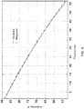
- Fig. 6 is a graph showing the design value and the measured value of the period length of the multilayer film with respect to the position of the first imaging mirror for vertical reflection.
- Fig. 7 is a graph showing the design value and the measured value of the period length of the multilayer film with respect to the position of the second imaging mirror for vertical reflection.
- Fig. 8 is a graph showing the design value and the measured value of the period length of the multilayer film with respect to the position of the first imaging mirror for horizontal reflection.
- Figure 9 is a graph showing the design value and the measured value of the period length of the multilayer film with respect to the position of the second imaging mirror for horizontal reflection.
- the straight line represents the design value of the period length corresponding to the position
- the circle represents the measured value of the period length for each position.
- the error was within 0.2 ⁇ .
- Fig. 10 is a graph showing the magnitude of the error of the surface shape with respect to the position of the second imaging mirror for horizontal reflection. As shown in Fig. 10 , the error of the surface shape in the second imaging mirror for horizontal reflection was within 1.5nm. Incidentally, the same results as the second imaging mirror for horizontal reflection was obtained for the surface shape of the other mirrors.
- the imaging type X-ray microscope 100 was assembled using the mirror manufactured with the accuracy of the above multilayer film.
- An X-ray source of CuKa was used.
- Specifications of the details of the mirror set constituting the reflecting mirror type X-ray lens unit 150 is as shown in the following table.
- a high-resolution X-ray camera Xsight XRM manufactured by Rigaku was used for the high-resolution X-ray detector 190.
- an X-ray image of a test chart for resolution evaluation was acquired.
- X-ray charts of thick film high-resolution types made by NTT-AT XRESO-50HC, smallest dimension of 50nm, pattern height of 500nm
- the pixel resolution of the calculated X-ray image was 23nm.
- the relationship between the magnification of the reflecting mirror type X-ray lens unit 150, the spatial resolution of the high-resolution X-ray detector 190 and the pixel resolution of the X-ray image is as shown in the following table.
- MAGNIFICATION RATIO OF IMAGING SYSTEM TIMES
- SPATIAL RESOLUTION OF DETECTING SYSTEM ⁇ m/pixel
- PIXEL RESOLUTION ⁇ m/pixel
- Figs. 11A and 11B are diagrams showing X-ray images of test charts for resolution evaluations when each exposure was respectively performed for 30 seconds and 150 seconds. As shown in Figs. 11A and 11B , in both X-ray images, 0.1 ⁇ m charts were distinguishable. However, the contrast clearly appeared in the exposure for 150 seconds than in the exposure for 30 seconds. As described above, even in the laboratory, measurement with a resolution of 100 nm or less becomes possible in several tens of seconds, and the imaging type X-ray microscope 100 has reached a practical product level as a laboratory device.
- Fig. 12 is a graph showing an X-ray image and a portion of the intensity distribution of the test chart for resolution evaluation when exposed for 1500 seconds. As shown in Fig. 12 , a part of the 50 nm chart pattern was distinguishable.
Landscapes
- Physics & Mathematics (AREA)
- Health & Medical Sciences (AREA)
- Chemical & Material Sciences (AREA)
- Pathology (AREA)
- Immunology (AREA)
- General Physics & Mathematics (AREA)
- General Health & Medical Sciences (AREA)
- Biochemistry (AREA)
- Analytical Chemistry (AREA)
- Life Sciences & Earth Sciences (AREA)
- Engineering & Computer Science (AREA)
- High Energy & Nuclear Physics (AREA)
- General Engineering & Computer Science (AREA)
- Theoretical Computer Science (AREA)
- Radiology & Medical Imaging (AREA)
- Pulmonology (AREA)
- Nuclear Medicine, Radiotherapy & Molecular Imaging (AREA)
- Spectroscopy & Molecular Physics (AREA)
- Analysing Materials By The Use Of Radiation (AREA)
Applications Claiming Priority (1)
| Application Number | Priority Date | Filing Date | Title |
|---|---|---|---|
| JP2020178363A JP7572033B2 (ja) | 2020-10-23 | 2020-10-23 | 結像型x線顕微鏡 |
Publications (1)
| Publication Number | Publication Date |
|---|---|
| EP3989240A1 true EP3989240A1 (en) | 2022-04-27 |
Family
ID=78528617
Family Applications (1)
| Application Number | Title | Priority Date | Filing Date |
|---|---|---|---|
| EP21203333.6A Pending EP3989240A1 (en) | 2020-10-23 | 2021-10-19 | Imaging type x-ray microscope |
Country Status (4)
| Country | Link |
|---|---|
| US (1) | US11885753B2 (enExample) |
| EP (1) | EP3989240A1 (enExample) |
| JP (2) | JP7572033B2 (enExample) |
| CN (1) | CN114509452A (enExample) |
Families Citing this family (4)
| Publication number | Priority date | Publication date | Assignee | Title |
|---|---|---|---|---|
| JP7572033B2 (ja) * | 2020-10-23 | 2024-10-23 | 株式会社リガク | 結像型x線顕微鏡 |
| JP2021087827A (ja) * | 2021-03-01 | 2021-06-10 | 株式会社三洋物産 | 遊技機 |
| WO2023203856A1 (ja) * | 2022-04-22 | 2023-10-26 | 株式会社リガク | 半導体検査装置、半導体検査システムおよび半導体検査方法 |
| KR102575501B1 (ko) * | 2022-09-05 | 2023-09-07 | 한국원자력연구원 | 반도체 패키징용 칩 정렬 장치 및 그 방법 |
Citations (7)
| Publication number | Priority date | Publication date | Assignee | Title |
|---|---|---|---|---|
| JPH01292297A (ja) * | 1988-05-19 | 1989-11-24 | Toshiba Corp | X線ミラー及びその製造方法 |
| JPH03140900A (ja) * | 1989-10-26 | 1991-06-14 | Olympus Optical Co Ltd | 結像型x線顕微鏡 |
| US5450463A (en) * | 1992-12-25 | 1995-09-12 | Olympus Optical Co., Ltd. | X-ray microscope |
| US6389101B1 (en) * | 1999-05-24 | 2002-05-14 | Jmar Research, Inc. | Parallel x-ray nanotomography |
| JP2004347463A (ja) * | 2003-05-22 | 2004-12-09 | Kawasaki Heavy Ind Ltd | 結像型x線顕微鏡 |
| US7394890B1 (en) | 2003-11-07 | 2008-07-01 | Xradia, Inc. | Optimized x-ray energy for high resolution imaging of integrated circuits structures |
| JP6478433B2 (ja) | 2015-09-25 | 2019-03-06 | 国立大学法人大阪大学 | X線顕微鏡 |
Family Cites Families (68)
| Publication number | Priority date | Publication date | Assignee | Title |
|---|---|---|---|---|
| DE3642457A1 (de) * | 1986-12-12 | 1988-06-30 | Zeiss Carl Fa | Roentgen-mikroskop |
| DE4027285A1 (de) * | 1990-08-29 | 1992-03-05 | Zeiss Carl Fa | Roentgenmikroskop |
| JPH05164899A (ja) * | 1991-12-19 | 1993-06-29 | Nikon Corp | 多層膜反射鏡 |
| JPH06250000A (ja) * | 1993-03-01 | 1994-09-09 | Olympus Optical Co Ltd | X線顕微鏡 |
| JPH06194500A (ja) * | 1992-12-25 | 1994-07-15 | Olympus Optical Co Ltd | X線顕微鏡 |
| DE4432811B4 (de) * | 1993-09-15 | 2006-04-13 | Carl Zeiss | Phasenkontrast-Röntgenmikroskop |
| DE69504004T2 (de) * | 1994-05-11 | 1999-05-27 | University Of Colorado, Boulder, Col. | Roentgenstrahlungsoptik mit streifendem lichteinfall und sphaerischen spiegeln |
| EP0873566B1 (de) * | 1996-01-12 | 2001-03-14 | Niemann, Bastian | Röntgenmikroskop mit zonenplatten |
| AU6762198A (en) * | 1997-03-18 | 1998-10-12 | Focused X-Rays Llc | Medical uses of focused and imaged x-rays |
| US6014423A (en) * | 1998-02-19 | 2000-01-11 | Osmic, Inc. | Multiple corner Kirkpatrick-Baez beam conditioning optic assembly |
| US6041099A (en) * | 1998-02-19 | 2000-03-21 | Osmic, Inc. | Single corner kirkpatrick-baez beam conditioning optic assembly |
| AU3474200A (en) * | 1999-01-26 | 2000-08-07 | Focused X-Rays Llc | X-ray interferometer |
| JP3741411B2 (ja) * | 1999-10-01 | 2006-02-01 | 株式会社リガク | X線集光装置及びx線装置 |
| US6332689B1 (en) * | 1999-12-14 | 2001-12-25 | Fujitsu Limited | Optical apparatus which uses a virtually imaged phased array to produce chromatic dispersion |
| US7119953B2 (en) * | 2002-12-27 | 2006-10-10 | Xradia, Inc. | Phase contrast microscope for short wavelength radiation and imaging method |
| US20070165782A1 (en) * | 2004-02-12 | 2007-07-19 | Tetsuya Makimura | Soft x-ray processing device and soft x-ray processing method |
| JP4123305B2 (ja) * | 2005-03-30 | 2008-07-23 | 株式会社ニコン | 画像作成方法および顕微鏡装置 |
| US7406151B1 (en) * | 2005-07-19 | 2008-07-29 | Xradia, Inc. | X-ray microscope with microfocus source and Wolter condenser |
| JP4860418B2 (ja) * | 2006-10-10 | 2012-01-25 | 株式会社リガク | X線光学系 |
| US7920676B2 (en) * | 2007-05-04 | 2011-04-05 | Xradia, Inc. | CD-GISAXS system and method |
| JP4861283B2 (ja) * | 2007-09-28 | 2012-01-25 | 株式会社リガク | X線回折装置およびx線回折方法 |
| US8836948B2 (en) * | 2009-01-29 | 2014-09-16 | The Regents Of The University Of California | High resolution structured illumination microscopy |
| JP5626750B2 (ja) * | 2009-08-04 | 2014-11-19 | 国立大学法人広島大学 | 測定装置及び測定方法 |
| DE102009044986A1 (de) * | 2009-09-24 | 2011-03-31 | Carl Zeiss Microimaging Gmbh | Mikroskop |
| US8249220B2 (en) * | 2009-10-14 | 2012-08-21 | Rigaku Innovative Technologies, Inc. | Multiconfiguration X-ray optical system |
| WO2011135819A1 (ja) * | 2010-04-26 | 2011-11-03 | 株式会社ニコン | 構造化照明顕微鏡装置 |
| CN103097878B (zh) * | 2010-09-10 | 2015-07-22 | 奥林巴斯株式会社 | 使用单个发光颗粒的光强度的光学分析方法 |
| JP5714861B2 (ja) * | 2010-10-07 | 2015-05-07 | 株式会社リガク | X線画像撮影方法およびx線画像撮影装置 |
| EP2629133A4 (en) * | 2010-10-14 | 2017-12-13 | Nikon Corporation | Structured illumination device, structured illumination microscope device, and surface shape measurement device |
| US8908087B2 (en) * | 2010-11-16 | 2014-12-09 | Nikon Corporation | Multiband camera, and multiband image capturing method |
| JP5751328B2 (ja) * | 2011-06-29 | 2015-07-22 | 株式会社ニコン | 構造化照明光学系および構造化照明顕微鏡装置 |
| CA2875680A1 (en) * | 2012-06-08 | 2013-12-12 | Rigaku Innovative Technologies, Inc. | Dual mode small angle scattering camera |
| WO2014005195A2 (en) * | 2012-07-05 | 2014-01-09 | Martin Russell Harris | Structured illumination microscopy apparatus and method |
| JP5888416B2 (ja) * | 2012-07-19 | 2016-03-22 | 株式会社ニコン | 構造化照明顕微鏡装置 |
| DE102012020240A1 (de) * | 2012-10-12 | 2014-04-17 | Carl Zeiss Microscopy Gmbh | Mikroskop und Verfahren zur SPIM Mikroskopie |
| EP2801855B1 (en) * | 2013-05-10 | 2019-07-17 | European Molecular Biology Laboratory | A microscope module for imaging a sample |
| JP6284073B2 (ja) * | 2013-07-12 | 2018-02-28 | 国立大学法人 東京大学 | 回転体ミラーを用いたx線集光システムの光学設計方法及びx線集光システム |
| JP6264377B2 (ja) * | 2013-07-17 | 2018-01-24 | 株式会社ニコン | 構造化照明装置及び構造化照明顕微鏡装置 |
| US10297359B2 (en) * | 2013-09-19 | 2019-05-21 | Sigray, Inc. | X-ray illumination system with multiple target microstructures |
| US10269528B2 (en) * | 2013-09-19 | 2019-04-23 | Sigray, Inc. | Diverging X-ray sources using linear accumulation |
| US10295485B2 (en) * | 2013-12-05 | 2019-05-21 | Sigray, Inc. | X-ray transmission spectrometer system |
| CN104575655A (zh) | 2013-10-10 | 2015-04-29 | 同济大学 | 一种针对多个工作能点响应的x射线多层膜结构 |
| JP6197880B2 (ja) * | 2013-12-12 | 2017-09-20 | 株式会社ニコン | 構造化照明顕微鏡、構造化照明方法、及びプログラム |
| DE102013021542A1 (de) * | 2013-12-18 | 2015-06-18 | Carl Zeiss Microscopy Gmbh | Mikroskop und Verfahren zur SPIM Mikroskopie |
| JP2015135463A (ja) * | 2013-12-19 | 2015-07-27 | オリンパス株式会社 | 顕微鏡装置、及び、顕微鏡システム |
| US9823203B2 (en) * | 2014-02-28 | 2017-11-21 | Sigray, Inc. | X-ray surface analysis and measurement apparatus |
| WO2016054118A1 (en) * | 2014-09-29 | 2016-04-07 | Howard Hughes Medical Institute | Non-linear structured illumination microscopy |
| US10181190B2 (en) * | 2014-11-04 | 2019-01-15 | Olympus Corporation | Microscope and microscope image acquisition method |
| US10007100B2 (en) * | 2014-11-04 | 2018-06-26 | Olympus Corporation | Light sheet illumination microscope and light sheet illumination method |
| JP6635052B2 (ja) * | 2015-02-05 | 2020-01-22 | 株式会社ニコン | 構造化照明顕微鏡、及び観察方法 |
| JP6417262B2 (ja) * | 2015-04-15 | 2018-11-07 | オリンパス株式会社 | シート照明顕微鏡 |
| JP6503221B2 (ja) * | 2015-05-13 | 2019-04-17 | オリンパス株式会社 | 3次元情報取得装置、及び、3次元情報取得方法 |
| JP6632852B2 (ja) * | 2015-10-06 | 2020-01-22 | 浜松ホトニクス株式会社 | X線撮像装置及びx線撮像方法 |
| JP2017090851A (ja) * | 2015-11-17 | 2017-05-25 | オリンパス株式会社 | シート照明顕微鏡、及び、シート照明方法 |
| US9943272B2 (en) * | 2016-07-23 | 2018-04-17 | Rising Star Pathway, a California Corporation | X-ray laser microscopy system and method |
| EP3312868A1 (en) * | 2016-10-21 | 2018-04-25 | Excillum AB | Structured x-ray target |
| US20190353802A1 (en) * | 2017-01-02 | 2019-11-21 | Koninklijke Philips N.V. | X-ray detector and x-ray imaging apparatus |
| EP3416181A1 (en) * | 2017-06-15 | 2018-12-19 | Koninklijke Philips N.V. | X-ray source and method for manufacturing an x-ray source |
| JP6857400B2 (ja) * | 2018-03-01 | 2021-04-14 | 株式会社リガク | X線発生装置、及びx線分析装置 |
| JP2019191168A (ja) * | 2018-04-23 | 2019-10-31 | ブルカー ジェイヴィ イスラエル リミテッドBruker Jv Israel Ltd. | 小角x線散乱測定用のx線源光学系 |
| JP6871629B2 (ja) * | 2018-06-29 | 2021-05-12 | 株式会社リガク | X線分析装置及びその光軸調整方法 |
| CN112638261B (zh) * | 2018-09-04 | 2025-06-27 | 斯格瑞公司 | 利用滤波的x射线荧光的系统和方法 |
| US11056308B2 (en) | 2018-09-07 | 2021-07-06 | Sigray, Inc. | System and method for depth-selectable x-ray analysis |
| JP7314068B2 (ja) * | 2020-01-24 | 2023-07-25 | キオクシア株式会社 | 撮像装置、画像生成装置及び撮像方法 |
| US11217357B2 (en) * | 2020-02-10 | 2022-01-04 | Sigray, Inc. | X-ray mirror optics with multiple hyperboloidal/hyperbolic surface profiles |
| WO2021237237A1 (en) * | 2020-05-18 | 2021-11-25 | Sigray, Inc. | System and method for x-ray absorption spectroscopy using a crystal analyzer and a plurality of detector elements |
| WO2022061347A1 (en) * | 2020-09-17 | 2022-03-24 | Sigray, Inc. | System and method using x-rays for depth-resolving metrology and analysis |
| JP7572033B2 (ja) * | 2020-10-23 | 2024-10-23 | 株式会社リガク | 結像型x線顕微鏡 |
-
2020
- 2020-10-23 JP JP2020178363A patent/JP7572033B2/ja active Active
-
2021
- 2021-10-14 US US17/501,378 patent/US11885753B2/en active Active
- 2021-10-19 EP EP21203333.6A patent/EP3989240A1/en active Pending
- 2021-10-21 CN CN202111230312.8A patent/CN114509452A/zh active Pending
-
2024
- 2024-04-23 JP JP2024070094A patent/JP7598681B2/ja active Active
Patent Citations (7)
| Publication number | Priority date | Publication date | Assignee | Title |
|---|---|---|---|---|
| JPH01292297A (ja) * | 1988-05-19 | 1989-11-24 | Toshiba Corp | X線ミラー及びその製造方法 |
| JPH03140900A (ja) * | 1989-10-26 | 1991-06-14 | Olympus Optical Co Ltd | 結像型x線顕微鏡 |
| US5450463A (en) * | 1992-12-25 | 1995-09-12 | Olympus Optical Co., Ltd. | X-ray microscope |
| US6389101B1 (en) * | 1999-05-24 | 2002-05-14 | Jmar Research, Inc. | Parallel x-ray nanotomography |
| JP2004347463A (ja) * | 2003-05-22 | 2004-12-09 | Kawasaki Heavy Ind Ltd | 結像型x線顕微鏡 |
| US7394890B1 (en) | 2003-11-07 | 2008-07-01 | Xradia, Inc. | Optimized x-ray energy for high resolution imaging of integrated circuits structures |
| JP6478433B2 (ja) | 2015-09-25 | 2019-03-06 | 国立大学法人大阪大学 | X線顕微鏡 |
Non-Patent Citations (2)
| Title |
|---|
| LADISLAV PINA ET AL: "Innovative X-ray optics for laboratory", PROCEEDINGS OF SPIE, IEEE, US, vol. 4781, 8 July 2002 (2002-07-08), pages 119 - 130, XP002619308, ISBN: 978-1-62841-730-2, DOI: 10.1117/12.450963 * |
| LIDER V V: "Kirkpatrick-Baez and Wolter X-Ray Focusing Optics (Review)", JOURNAL OF SURFACE INVESTIGATION : X-RAY, SYNCHROTRON AND NEUTRON TECHNIQUES, NEW VORK : PLEIADES PUBL, US, vol. 13, no. 4, 28 August 2019 (2019-08-28), pages 670 - 682, XP036874045, ISSN: 1027-4510, [retrieved on 20190828], DOI: 10.1134/S102745101904027X * |
Also Published As
| Publication number | Publication date |
|---|---|
| CN114509452A (zh) | 2022-05-17 |
| JP2022069273A (ja) | 2022-05-11 |
| US11885753B2 (en) | 2024-01-30 |
| JP7598681B2 (ja) | 2024-12-12 |
| JP2024097032A (ja) | 2024-07-17 |
| JP7572033B2 (ja) | 2024-10-23 |
| US20220128487A1 (en) | 2022-04-28 |
Similar Documents
| Publication | Publication Date | Title |
|---|---|---|
| US11885753B2 (en) | Imaging type X-ray microscope | |
| JP7427772B2 (ja) | 波長分解軟x線反射率測定に基づく半導体計測のための方法及びシステム | |
| US9846132B2 (en) | Small-angle scattering X-ray metrology systems and methods | |
| US9383324B2 (en) | Laboratory X-ray micro-tomography system with crystallographic grain orientation mapping capabilities | |
| US7183547B2 (en) | Element-specific X-ray fluorescence microscope and method of operation | |
| US6389101B1 (en) | Parallel x-ray nanotomography | |
| JP5838114B2 (ja) | X線トポグラフィ装置 | |
| CN118624653A (zh) | 小角度x射线散射测量 | |
| Schroer et al. | Beryllium parabolic refractive x-ray lenses | |
| Tkachuk et al. | High-resolution x-ray tomography using laboratory sources | |
| US5864599A (en) | X-ray moire microscope | |
| JPWO2004061428A1 (ja) | 空孔または粒子サイズ分布測定装置 | |
| US20250251355A1 (en) | Semiconductor inspection apparatus, semiconductor inspection system and semiconductor inspection method | |
| US11894160B2 (en) | Light field X-ray optics | |
| Pantojas et al. | A polycapillary-based X-ray optical system for diffraction applications | |
| Storm et al. | Multilayer optics for Mo-radiation-based crystallography | |
| WO2021008819A1 (en) | Microscopy system | |
| US20260092883A1 (en) | Soft X-Ray Tools for Semiconductor Metrology Applications | |
| JPH10221500A (ja) | 軟x線検査装置 | |
| TW202601680A (zh) | 用於產生聚焦x射線束之系統及方法 | |
| Ye et al. | A transmission grating extreme ultraviolet spectrometer using a gradient-reflectivity Al/Zr multilayer mirror for the range of 24–32 nm | |
| JPH0560702A (ja) | X線を用いた断層像撮像方法及び装置 | |
| JP2024159579A (ja) | 複数の角度入力面を有するx線回折イメージング検出器 | |
| Bakulin | Imaging of hard X-rays with a multilayer Kirkpatrick-Baez CCD microscope in the laboratory and at the synchrotron | |
| Pina | Reflective Optical Structures and Imaging Detector Systems |
Legal Events
| Date | Code | Title | Description |
|---|---|---|---|
| PUAI | Public reference made under article 153(3) epc to a published international application that has entered the european phase |
Free format text: ORIGINAL CODE: 0009012 |
|
| STAA | Information on the status of an ep patent application or granted ep patent |
Free format text: STATUS: THE APPLICATION HAS BEEN PUBLISHED |
|
| AK | Designated contracting states |
Kind code of ref document: A1 Designated state(s): AL AT BE BG CH CY CZ DE DK EE ES FI FR GB GR HR HU IE IS IT LI LT LU LV MC MK MT NL NO PL PT RO RS SE SI SK SM TR |
|
| STAA | Information on the status of an ep patent application or granted ep patent |
Free format text: STATUS: REQUEST FOR EXAMINATION WAS MADE |
|
| 17P | Request for examination filed |
Effective date: 20221025 |
|
| RBV | Designated contracting states (corrected) |
Designated state(s): AL AT BE BG CH CY CZ DE DK EE ES FI FR GB GR HR HU IE IS IT LI LT LU LV MC MK MT NL NO PL PT RO RS SE SI SK SM TR |
|
| STAA | Information on the status of an ep patent application or granted ep patent |
Free format text: STATUS: EXAMINATION IS IN PROGRESS |
|
| 17Q | First examination report despatched |
Effective date: 20250805 |