EP3764399B1 - Display device and display system - Google Patents
Display device and display system Download PDFInfo
- Publication number
- EP3764399B1 EP3764399B1 EP20181964.6A EP20181964A EP3764399B1 EP 3764399 B1 EP3764399 B1 EP 3764399B1 EP 20181964 A EP20181964 A EP 20181964A EP 3764399 B1 EP3764399 B1 EP 3764399B1
- Authority
- EP
- European Patent Office
- Prior art keywords
- pixel
- light
- lens
- display device
- layer
- Prior art date
- Legal status (The legal status is an assumption and is not a legal conclusion. Google has not performed a legal analysis and makes no representation as to the accuracy of the status listed.)
- Active
Links
Images


Classifications
-
- H—ELECTRICITY
- H10—SEMICONDUCTOR DEVICES; ELECTRIC SOLID-STATE DEVICES NOT OTHERWISE PROVIDED FOR
- H10K—ORGANIC ELECTRIC SOLID-STATE DEVICES
- H10K59/00—Integrated devices, or assemblies of multiple devices, comprising at least one organic light-emitting element covered by group H10K50/00
- H10K59/30—Devices specially adapted for multicolour light emission
- H10K59/35—Devices specially adapted for multicolour light emission comprising red-green-blue [RGB] subpixels
- H10K59/353—Devices specially adapted for multicolour light emission comprising red-green-blue [RGB] subpixels characterised by the geometrical arrangement of the RGB subpixels
-
- H—ELECTRICITY
- H10—SEMICONDUCTOR DEVICES; ELECTRIC SOLID-STATE DEVICES NOT OTHERWISE PROVIDED FOR
- H10K—ORGANIC ELECTRIC SOLID-STATE DEVICES
- H10K59/00—Integrated devices, or assemblies of multiple devices, comprising at least one organic light-emitting element covered by group H10K50/00
- H10K59/10—OLED displays
- H10K59/12—Active-matrix OLED [AMOLED] displays
- H10K59/121—Active-matrix OLED [AMOLED] displays characterised by the geometry or disposition of pixel elements
-
- H—ELECTRICITY
- H10—SEMICONDUCTOR DEVICES; ELECTRIC SOLID-STATE DEVICES NOT OTHERWISE PROVIDED FOR
- H10K—ORGANIC ELECTRIC SOLID-STATE DEVICES
- H10K50/00—Organic light-emitting devices
- H10K50/80—Constructional details
- H10K50/85—Arrangements for extracting light from the devices
- H10K50/858—Arrangements for extracting light from the devices comprising refractive means, e.g. lenses
-
- H—ELECTRICITY
- H10—SEMICONDUCTOR DEVICES; ELECTRIC SOLID-STATE DEVICES NOT OTHERWISE PROVIDED FOR
- H10K—ORGANIC ELECTRIC SOLID-STATE DEVICES
- H10K59/00—Integrated devices, or assemblies of multiple devices, comprising at least one organic light-emitting element covered by group H10K50/00
- H10K59/30—Devices specially adapted for multicolour light emission
- H10K59/38—Devices specially adapted for multicolour light emission comprising colour filters or colour changing media [CCM]
-
- H—ELECTRICITY
- H10—SEMICONDUCTOR DEVICES; ELECTRIC SOLID-STATE DEVICES NOT OTHERWISE PROVIDED FOR
- H10K—ORGANIC ELECTRIC SOLID-STATE DEVICES
- H10K59/00—Integrated devices, or assemblies of multiple devices, comprising at least one organic light-emitting element covered by group H10K50/00
- H10K59/80—Constructional details
- H10K59/875—Arrangements for extracting light from the devices
- H10K59/879—Arrangements for extracting light from the devices comprising refractive means, e.g. lenses
-
- H—ELECTRICITY
- H10—SEMICONDUCTOR DEVICES; ELECTRIC SOLID-STATE DEVICES NOT OTHERWISE PROVIDED FOR
- H10K—ORGANIC ELECTRIC SOLID-STATE DEVICES
- H10K59/00—Integrated devices, or assemblies of multiple devices, comprising at least one organic light-emitting element covered by group H10K50/00
- H10K59/10—OLED displays
- H10K59/12—Active-matrix OLED [AMOLED] displays
- H10K59/126—Shielding, e.g. light-blocking means over the TFTs
Definitions
- the present disclosure relates to a display device and a display system.
- wearable display devices such as Augmented Reality (AR), Virtual Reality (VR), and Mixed Reality (MR) devices.
- AR Augmented Reality
- VR Virtual Reality
- MR Mixed Reality
- the wearable display devices have a problem in that the size and the weight need to be decreased.
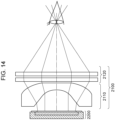
- FIG. 14 illustrates the display system disclosed in PTL 1.
- the display system includes a display device 2200.
- Light that is emitted from the display device 2200 passes through an ocular optical system 2100 and is directly guided to the pupils of a user.
- the ocular optical system 2100 includes a first lens group 2110 and a second lens group 2120.
- the use of the display system disclosed in PTL 1 allegedly enables a small, lightweight display system having a maximum angle of view of more than 80 degrees to be provided.
- the display device is not sufficiently considered.
- WO 2012/088260 A2 discusses light extraction blocks, and OLED lighting panels using light extraction blocks, in which the light extraction blocks include various curved shapes that provide improved light extraction properties compared to parallel emissive surface, and a thinner form factor and better light extraction than a hemisphere.
- Lighting systems described may include a light source with an OLED panel.
- a light extraction block with a three-dimensional light emitting surface may be optically coupled to the light source.
- the three-dimensional light emitting surface of the block may include a substantially curved surface, with further characteristics related to the curvature of the surface at given points.
- a first radius of curvature corresponding to a maximum principal curvature k 1 at a point p on the substantially curved surface may be greater than a maximum height of the light extraction block.
- a maximum height of the light extraction block may be less than 50% of a maximum width of the light extraction block.
- Surfaces with cross sections made up of line segments and inflection points may also be fit to approximated curves for calculating
- CN 109 216 584 A discusses a flexible OLED display panel, comprising a bent display unit, wherein the bent display unit comprises a TFT array layer, a light emitting structure layer having a plurality of sub-pixels and an encapsulation structure layer, and the encapsulation structure layer comprises a refraction structure corresponding to an area where the sub-pixels are located.
- the invention realizes the angle deflection of the light emitted by the bent display unit through the arrangement of the refraction structure in the packaging structure, so that the angle of the light emitted by the bent display unit and the angle of the light emitted by the plane display area are the same.
- US 2010/182222 A1 discusses a light-emitter includes a first electrode layer, a second electrode layer, and a light-emitting layer located between the first and second electrode layers.
- a gradient index lens is located proximate to the second electrode layer opposite the light-emitting layer and comprises a plurality of concentric parts.
- the concentric parts are grouped into a central zone and annular zones.
- Each annular zone includes at least two of the concentric parts.
- One of the concentric parts included in each annular zone has a refractive index different from a refractive index of another of the concentric parts.
- a wavelength of light emitted from the light-emitting layer is greater than a radius of the central zone and a width of each annular zone.
- An effective refractive index of each annular zone decreases in an outward direction from a center of the gradient index lens.
- US 2017/133637 A1 discusses a display device including pixels disposed on a substrate, and a lens layer disposed on the substrate, the lens layer including Fresnel lenses respectively corresponding to the pixels.
- Each of the Fresnel lenses includes Fresnel zones disposed adjacent to each other in a radial direction with respect to a center of a corresponding Fresnel lens, and refractive indices of each of the Fresnel zones change stepwise along the radial direction.
- US 2004/150329 A1 discusses a display unit which can improve emission efficiency of lights for image display, and assure luminance of display images.
- the display unit comprises micro prisms which are arranged in the positions corresponding to organic EL devices, and which have a high refraction index to refract a light, and auxiliary prisms with a low refraction index which are embedded in voids between each micro prism.
- a light volume of the light viewed as an image in the direction facing an organic EL display (facing direction) is a total of a light volume of a light essentially emitted from the organic EL device in the facing direction, and lights which are directed in the facing direction by utilizing refraction phenomenon based on differences of refraction index between the micro prism and the auxiliary prism.
- an emission volume of the light in the facing direction is increased by the light volumes of the lights.
- a display device that is capable of improving the quality of display is provided.
- the present invention in its first aspect provides a display device as specified in claims 1 to 9.
- the present invention in its second aspect provides a display system as specified in claims 10 and 11.
- an optical lens system 2100 is disposed between a display device and the eyes of a user.
- the optical lens system uses luminous flux that is emitted in a direction perpendicular thereto as light that is to be viewed by the eyes of the user.
- luminous flux that is emitted in a direction inclined at an increased angle of elevation is used as the light that is to be viewed by the eyes of the user.
- the luminous flux that is emitted in the perpendicular direction is more likely to be useless and is more unlikely to be used.
- the useless luminous flux that is not used becomes an unintentional reflection component in the optical lens system and can result in degradation in display quality such as a ghost and color mixing.
- the present inventors have arrived at such an idea and have conceived a solution as follows: regarding optical members of a display device, the structure of a first optical member that is disposed at a central portion of a display region is differentiated from the structure of a second optical member that is disposed at a peripheral portion of the display region.
- the embodiments for carrying out the present disclosure will be described below with reference to the drawings.
- common components in the drawings are designated by common reference characters. Accordingly, the drawings are mutually referred to describe the common components, and a description of a component that is designated by a common reference character is appropriately omitted.
- FIG. 1 illustrates a plan view of a display device 100.
- arrangement is illustrated when the display device 100 is viewed in a direction perpendicular to a main surface of a semiconductor substrate 16 (direction of a normal to the main surface).
- overlapping members can be seen through.
- the display device 100 has an effective pixel region 11 in which effective pixels are provided and a periphery circuit region 13 that is located around the effective pixel region 11.
- the effective pixel region 11 is quadrilateral.
- periphery circuits are disposed.
- the periphery circuits of the display device include a drive circuit that drives the effective pixels and a processing circuit, such as a DAC (digital-to-analog conversion circuit) that processes signals that are inputted into the effective pixels.
- DAC digital-to-analog conversion circuit
- a non-effective pixel region 12 in which non-effective pixels are provided is located between the periphery circuit region 13 and the effective pixel region 11.
- the non-effective pixels include a dummy pixel, a reference pixel, a test pixel, and a monitor pixel that do not function as an effective pixel.
- Each pixel that is provided in the effective pixel region 11 includes a light-emitting layer (not illustrated) and an optical member (not illustrated) that is transparent to light from the light-emitting layer.
- An example of the optical member is a microlens.
- a color filter (not illustrated) may be disposed between the light-emitting layer and the optical member.
- Microlenses each of which serves as the optical member may be continuously disposed not only in the effective pixel region 11 but also in the non-effective pixel region 12. The microlenses may be continuously disposed not only in the non-effective pixel region 12 but also in the periphery circuit region 13.
- the microlenses are preferably continuously disposed up to the periphery circuit region 13.
- the microlenses are disposed in the effective pixel region 11, the non-effective pixel region 12, and the periphery circuit region 13.
- the outer edge of the region in which the microlenses are disposed is designated by the reference character 17 in FIG. 1 .
- the color filters are disposed, as illustrated in FIG.
- color filters may be continuously disposed not only in the effective pixel region 11 but also in the non-effective pixel region 12 and the periphery circuit region 13.
- the outer edge of the region in which the color filters are disposed is designated by the reference character 14 in FIG. 1 .
- a single unit of each microlens has a predetermined size.
- Each color filter can have a freely determined size. As illustrated in FIG. 1 , the outer edge 14 of the region in which the color filters are disposed is located outside the outer edge 17 of the region in which the microlenses are disposed.
- a transparent plate 15 illustrated in FIG. 1 for example, a glass substrate faces the effective pixel region 11, the non-effective pixel region 12, and the periphery circuit region 13 that are formed on the semiconductor substrate 16.
- the transparent plate 15 is joined to, for example, the effective pixel region 11 that is formed on the semiconductor substrate 16 by using a joint member.
- the joint member can include a matrix composed of resin and a filler that disperses in the matrix.
- the filler may be resin.
- connection region 18 illustrated in FIG. 1 is a connection region (pad) that is provided to connect an output signal from the display device 100 to an external device.
- FIG. 2A illustrates an example of two-dimensional arrangement of display pixels that are provided in the effective pixel region 11.
- the pixels are provided in delta arrangement of a honeycomb structure.
- a set is made by three pixels of an R-pixel (red-light-emitting pixel), a G-pixel (green-light-emitting pixel), and a B-pixel (blue-light-emitting pixel).
- the pixels described according to the present embodiment are referred to as sub-pixels or secondary pixels.
- a pixel 210 that is designated by the character M is located at the center of the effective pixel region 11.
- pixels 220, 230, and 240 are arranged in this order in a positive X-direction (right-hand side direction), and pixels 250, 260, and 270 are arranged in this order in a negative X-direction (left-hand side direction).
- One or more pixels are located between the pixels illustrated in the figure. However, the one or more pixels that are located between the pixels illustrated in FIG. 2A are omitted for convenience.
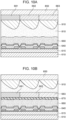
- FIG. 2B and FIG. 2C illustrate a sectional view taken along line A-A' in FIG. 2A .
- FIG. 2B illustrates the pixels 210, 220, 230, and 240 and microlenses 215, 225, 235, and 245 that are included in the respective pixels.
- FIG. 2C illustrates the pixels 210, 250, 260, and 270 and the microlens 215 and microlenses 255, 265, and 275 that are included in the respective pixels.
- the XY plane is a plane in an orthographic projection of each microlens that is the optical member on the light-emitting layer.
- the orthographic projection is referred to as a plan view.
- contour lines that connect positions at which heights in a Z-direction are equal to each other are illustrated.
- E1 represents an end portion of each microlens facing the central portion.
- E2 represents an end portion of the microlens facing a peripheral portion.
- C represents the center of the microlens.
- T represents an apex of the microlens.
- the end portions of the microlens are located at positions at which the height in the Z-direction is the minimum height in the sectional view.
- the center of the microlens is the center of gravity of a shape that is formed by lines that connect the end portions of the microlens on the XY plane.
- the height of the microlens is the position of the highest portion in the Z-direction.
- the center C and the apex T of the microlens 215 that is included in the pixel 210 (pixel M) coincide with each other on the XY plane. To coincide means to substantially coincide. A slight difference due to a manufacturing error is tolerated.
- the microlens 215 is a symmetrical microlens that has 2-fold rotational symmetry on the XY plane.
- the microlenses 225, 235, 245, 255, 265, and 275 are arranged such that the center C and the apex T shift with respect to each other on the XY plane.
- the microlenses 225 to 275 are asymmetrical microlenses that do not have the 2-fold rotational symmetry on the XY plane.
- To be nearer to the periphery means to be nearer to an edge portion of the semiconductor substrate 16 when viewed from the central portion of the effective pixel region 11.
- a distance 226 (first distance) in the positive X-direction is equal to the distance between the center C and the apex T in the X-direction.
- a distance 236 (second distance) is equal to the distance between the center C and the apex T in the X-direction.
- a distance 246 (third distance) is equal to the distance between the center C and the apex T in the X-direction.
- the distance 236 in the pixel 230 that is located nearer than the pixel 220 to the periphery is longer than the distance 226 in the pixel 220 that is located near the center of the effective pixel region.
- the distance 246 in the pixel 240 that is located nearer than the pixel 230 to the periphery is longer than the distance 236.
- a distance 256 (fourth distance) in the negative X-direction is equal to the distance between the center C and the apex T in the X-direction.
- a distance 266 (fifth distance) is equal to the distance between the center C and the apex T in the X-direction.
- a distance 276 (sixth distance) is equal to the distance between the center C and the apex T in the X-direction.
- the distance 266 in the pixel 260 that is located nearer than the pixel 250 to the periphery is longer than the distance 256 in the pixel 250 that is located near the center of the effective pixel region.
- the distance 276 in the pixel 270 that is located nearer than the pixel 260 to the periphery is longer than the distance 266.
- FIG. 3A to FIG. 3C illustrate the effects of the microlenses described with reference to FIG. 2A to FIG. 2C .
- FIG. 3B and FIG. 3C as the position is closer to the periphery away from the central portion of the effective pixel region, an angle at which the luminous flux that is emitted from the light-emitting layer in the perpendicular direction is refracted by each microlens increases. That is, as the position is closer to the peripheral portion away from the central portion, refractive power (power) against the luminous flux that is emitted from the light-emitting layer in the perpendicular direction increases.
- the radiation solid angle of the luminous flux that is emitted from the light-emitting layer can be concentrated within a solid angle that is used in the optical lens system, and the use efficiency of light can be improved.
- Luminous flux that is not used in the optical lens system can be reduced, and a ghost and color mixing can be inhibited from occurring due to an unintentional reflection component in the optical lens system.
- a display device that is capable of improving the quality of display can be provided.
- FIG. 4B illustrates a sectional view taken along line B-B' in FIG. 4A .
- the line B-B' extends in a direction (second direction) intersecting the X-direction (first direction) at a first angle.
- pixels 320, 330, and 340 are arranged in a direction (B'-direction) from the pixel 210 toward the periphery.
- Microlenses 325, 335, and 345 are included in the respective pixels 320, 330, and 340.
- a distance 336 is longer than a distance 326, and a distance 346 is longer than the distance 336.
- the angle at which the luminous flux that is emitted from the light-emitting layer in the perpendicular direction is refracted by each microlens increases as the position is closer to the periphery away from the central portion of the effective pixel region. This enables a display device that is capable of improving the quality of display to be provided.
- pixels arranged in a B-direction including the pixel 210 include microlenses that are line-symmetrical to the microlenses illustrated in FIG. 4B .
- FIG. 5B and FIG. 6B described below.
- FIG. 5B illustrates a sectional view taken along line C-C' in FIG. 5A .
- the line C-C' extends in a direction (third direction) intersecting the X-direction (first direction) at a second angle.
- pixels 420, 430, and 440 are arranged in a direction (C'-direction) from the pixel 210 toward the periphery.
- Microlenses 425, 435, and 445 are included in the respective pixels 420, 430, and 440.
- a distance 436 is longer than a distance 426, and a distance 446 is longer than the distance 436.
- the angle at which the luminous flux that is emitted from the light-emitting layer in the perpendicular direction is refracted by each microlens increases as the position is closer to the periphery away from the central portion of the effective pixel region. This enables a display device that is capable of improving the quality of display to be provided.
- FIG. 6B illustrates a sectional view taken along line D-D' in FIG. 6A .
- the line D-D' extends in a direction (fourth direction) perpendicular to the X-direction (first direction).
- pixels 520, 530, and 540 are arranged in a direction (D'-direction) from the pixel 210 toward the periphery.
- Microlenses 525, 535, and 545 are included in the respective pixels 520, 530, and 540.
- a distance 536 is longer than a distance 526, and a distance 546 is longer than the distance 536.
- the angle at which the luminous flux that is emitted from the light-emitting layer in the perpendicular direction is refracted by each microlens increases as the position is closer to the periphery away from the central portion of the effective pixel region. This enables a display device that is capable of improving the quality of display to be provided.
- the asymmetrical microlenses described above can be formed by light exposure and development processes. Specifically, a film (photoresist film) is formed by using a material for forming the microlenses, and the photoresist film is exposed to light and developed by using a mask that has continuous variations in gradation.
- a mask can be a gray mask or an area gradation mask that is manufactured by using a light-shielding film having a resolution equal to or less than the resolution of a light exposure device and that enables an imaging plane to be irradiated with light having continuous gradation by changing dot density distribution.
- each microlens can be adjusted by performing an etch back process on the microlens that is formed by the light exposure and development processes.
- the asymmetrical microlenses can be formed without performing the light exposure and development processes.
- the asymmetrical microlenses can be formed by forming resin on small microlenses and reflowing the resin.
- the temperature in a reflow process is set to a predetermined temperature or less.
- the predetermined temperature or less means 120°C or less.
- FIG. 7A to FIG. 7D illustrate respective pixel structures of the pixels 210 to 240 illustrated in FIG. 2 .
- FIG. 7A to FIG. 7D differ from each other in the shapes of the microlenses 215 to 245. The differences are described above. Common components in FIG. 7A to FIG. 7D will now be described.
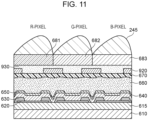
- a wiring structure 615 is disposed on a silicon substrate 610, and a first electrode 620 is disposed on the wiring structure 615.
- a separation portion 630 (banks) is disposed between the first electrode 620 and a first electrode of the pixels adjacent to each other.
- An organic layer 640 as the light-emitting layer and a second electrode 650 are disposed above the first electrode 620.
- a sealing layer 660, a planarizing layer 670, and a color filter 680 are disposed above the second electrode 650.
- the silicon substrate 610 includes a switching circuit such as a transistor.
- the wiring structure 615 includes wiring layers of, for example, an aluminum layer and a copper layer, a via plug, and a contact plug.
- An insulating film that insulates wiring lines from each other is disposed between the wiring layers.
- the insulating film includes a silicon oxide layer, a silicon nitride layer, or a silicon carbide layer.
- a silicon oxynitride and a silicon carbonitride that contain nitrogen and silicon as main elements are kinds of a silicon nitride.
- the first electrode 620 is preferably composed of a metal material that has a reflectance of 70% or more at a light-emitting wavelength.
- Metals such as Al and Ag, an alloy thereof that contains Si, Cu, Ni, or Nd, ITO, IZO, AZO, and IGZO can be used.
- the light-emitting wavelength described herein means a spectrum range of light that is emitted from the organic layer 640.
- the first electrode 620 may be a multilayer electrode including a barrier electrode composed of a metal such as Ti, W, Mo, or Au or an alloy thereof, provided that the reflectance is higher than a desired reflectance.
- a multilayer electrode including a transparent oxide film electrode such as an ITO or IZO electrode may be acceptable.
- the first electrode 620 may be a transparent conductive film, and a reflection layer may be disposed on a lower portion of the first electrode 620.
- the transparent conductive film can include ITO, IZO, AZO, and IGZO films.
- an optical adjustment layer may be disposed between the reflection layer and the transparent conductive film to optimize an optical distance.
- the optical film thickness of the optical adjustment layer differs among the R-pixel, the G-pixel, and the B-pixel.
- the optical adjustment layer is composed of, for example, a silicon nitride (SiN), a silicon oxynitride (SiON), or a silicon oxide (SiO).
- the organic layer 640 can be formed by a known method such as a deposition method or a spin coating method.
- the organic layer 640 may include layers. Examples of the layers include a hole injection layer, a hole transport layer, an electron-blocking layer, a light-emitting layer, a hole-blocking layer, an electron transport layer, and an electron injection layer.
- the organic layer 640 emits light when holes that are injected from an anode and electrons that are injected from a cathode are recombined in the organic layer.
- the organic layer may have a single layer structure or a multilayer structure.
- the organic layer can contain a red-light-emitting material, a green-light-emitting material, or a blue-light-emitting material at any position.
- the white color can be obtained by mixing light-emitting colors.
- the second electrode 650 is disposed on the organic layer 640 and has transparency.
- the second electrode 650 may be composed of a semi-transparent material that has properties allowing a part of light from the organic layer 640 to pass therethrough and another part of the light to be reflected (that is, semi-transparent, semi-reflective properties).
- Examples of the material of the second electrode 650 include transparent materials (ITO and IZO) such as transparent conductive oxides, metals such as aluminum, silver, and gold, alkali metals such as lithium and cesium, alkaline earth metals such as magnesium, calcium, and barium, and a semi-transparent material consisting of an alloy material that contains these metal materials.
- the semi-transparent material preferably contains magnesium or silver as a main component.
- the second electrode 650 may have a multilayer structure composed of any one of the above materials, provided that the material has preferable transmittance.
- the second electrode 650 may be integrally formed with the pixels and may be shared.
- the sealing layer 660 preferably contains an inorganic material that has translucency and that is less transparent to oxygen and water from the outside.
- inorganic materials such as a silicon nitride (SiN), a silicon oxynitride (SiON), a silicon oxide (SiOx), an aluminum oxide (Al 2 O 3 ), and a titanium oxide (TiO 2 ) are preferable.
- SiN, SiON, and Al 2 O 3 inorganic materials are preferable particularly in the perspective of sealing performance.
- the sealing layer 660 is preferably formed by using a chemical vapor deposition method (CVD method), an atomic layer deposition method (ALD method), or a spattering method.
- the sealing layer 660 may have a single layer structure or a multilayer structure that is obtained by a combination of the above materials and a formation method, provided that the sealing layer has sufficient water-shielding performance.
- a display device can inhibit color mixing due to stray light toward an aspherical microlens of an adjacent pixel from occurring more effectively as the distances between the organic layer 640 and the microlenses 215 to 245 decrease. Accordingly, a sealing film composed of, for example, aluminum oxide (Al 2 O 3 ) that is formed by the atomic layer deposition method (ALD method) and that has excellent coverage performance even when being thin is preferably used.
- the planarizing layer 670 can include a resin layer that has translucency.
- the planarizing layer can be formed by using a spin coating method.
- the color filter 680 is transparent to different colors.
- An example thereof is a color filter that is transparent to red light, green light, and blue light.
- a color filter that is transparent to cyan light, magenta light, and yellow light is also acceptable.
- the color filter 680 is transparent to green light. A part of the color filter or the entire color filter may be omitted.
- the color filters that are patterned in red, green, and blue are disposed in the effective pixel region 11 and the non-effective pixel region 12.
- the periphery circuit region 13 may include a region in which only a monochromatic color filter is disposed.
- a 100 ⁇ m or more region extending from the outer edge 14 of the region in which the color filters are disposed may be a region in which only a color filter that is transparent to blue light is disposed.
- FIG. 8A illustrates the structure of a light-emitting element that includes an R-pixel, a G-pixel, and a B-pixel.
- the R-pixel includes a color filter 681 that is selectively transparent to red.
- the G-pixel includes a color filter 682 that is selectively transparent to green.
- the B-pixel includes a color filter 683 that is selectively transparent to blue.
- the RGB-pixels adjacent to each other include respective microlenses 245 that have a shape common to each other. That is, asymmetrical microlenses that are included in the pixels adjacent to each other do not necessarily have different shapes.
- the effective pixel region is divided into three or more blocks, which are referred to as a first block, a second block, and a third block in this order in a direction from the central portion of the effective pixel region toward the periphery.
- a pixel that belongs to the first block may include the microlens 215, a pixel that belongs to the second block may include the microlens 225, and a pixel that belongs to the third block may include the microlens 235.
- the microlenses that are included in the pixels adjacent to each other in the second block and the third block have the same shape. To be the same described herein means to be substantially the same, and a design error is tolerated.
- an asymmetrical microlens that has a distance that falls between the distance 226 of the microlens 225 and the distance 236 of the microlens 235 may be provided.
- the asymmetrical microlenses that are included in the pixels adjacent to each other have different shapes.
- the centers of the microlenses 245 coincide with the centers of the respective pixels. However, the centers of the microlenses 245 may shift toward the periphery of the effective pixel region away from the centers of the respective pixels. The distance at which the centers of the microlens 245 shift may be gradually increased as the positions of the pixels are closer to the periphery away from the center of the effective pixel region.
- each microlens The angle at which the luminous flux that is emitted from the light-emitting layer in the perpendicular direction is refracted by each microlens increases as the position is closer to the periphery away from the central portion of the effective pixel region.
- an asymmetrical microlens illustrated in FIG. 2 in Japanese Patent Laid-Open No. 2007-335723 may be used.
- the asymmetrical microlens is called a teardrop microlens.
- Each microlens illustrated in FIG. 2A to FIG. 6B in the present disclosure corresponds to a microlens illustrated in FIG. 3(a) in Japanese Patent Laid-Open No. 2015-012488 .
- each microlens illustrated in FIG. 2A to FIG. 6B in the present disclosure occupies a pixel area larger than that of the teardrop microlens and enables light to be more efficiently focused.
- the outer edges of the microlenses 225, 235, and 245 include sides extending in the Y-direction on the XY plane. That is, the outer edges of the microlenses include the sides extending in the second direction (Y-direction) intersecting the first direction (X-direction) in which the microlenses are arranged.
- the teardrop microlens does not have a side extending in the Y-direction.
- the pixel area that is occupied by the teardrop microlens is smaller than the area that is occupied by each microlens illustrated in FIG. 2A to FIG. 6B in the present disclosure.
- the relationship of the magnitude of the occupied area can be understood by comparing FIG. 4(a) and FIG. 4(b) in Japanese Patent Laid-Open No. 2015-012488 .
- Japanese Patent Laid-Open No. 2007-335723 and Japanese Patent Laid-Open No. 2015-012488 disclose microlenses that are used for an imaging apparatus and different use from the use of the microlenses for the display device according to the present embodiment.
- FIG. 8B differs from FIG. 8A in that the color filters 681 to 683 are disposed above the microlenses 245.
- a layer 700 is disposed between the microlenses 245 and the color filters 681 to 683.
- the layer 700 may be composed of resin to function as a planarizing layer and function as an adhesive that causes the color filters 681 to 683 and the microlenses 245 to adhere to each other.
- the resin may have a single layer, or a resin layer for the planarizing layer and a resin layer for the adhesive may be functionally separated from each other and may be separated layers.
- the layer 700 may be an air gap layer (gas layer).
- the layer 700 is an air gap layer
- the difference in refractive indices between the microlenses 245 and the layer 700 can be ensured. Accordingly, the refractive power (power) of the microlenses 245 can be increased, and a display device that is capable of improving the quality of display can be provided.
- FIG. 9A differs from FIG. 8A in that other microlenses 800 are disposed between the microlenses 245 and the organic layer 640.
- the microlenses 800 are additionally provided. This enables a display device that is capable of improving the quality of display to be provided.
- a layer 810 may be a resin layer or an air gap layer as in the layer 700.
- the microlenses 800 are asymmetrical microlenses but may be symmetrical microlenses, and the centers of the microlenses may shift toward the periphery of the effective pixel region away from the centers of the pixels.
- the asymmetrical microlenses each of which has the shifting center may be used.
- FIG. 9B differs from FIG. 9A in that the microlenses 245 have a convex shape toward the organic layer 640 that is the light-emitting layer.
- the refractive index of the resin layer 810 is smaller than the refractive indices of the microlenses 800 and the microlenses 245. This enables the luminous flux that is emitted from the light-emitting layer in the perpendicular direction to be refracted in the same direction by using the microlenses 800 and the microlenses 245.
- the microlenses 245 have a convex shape toward the light-emitting layer.
- FIG. 10A differs from FIG. 8A in that microlenses 910 and the color filters 681 to 683 are secured to a substrate 850 that differs from the silicon substrate 610. Components from the wiring structure 615 to the sealing layer 660 are formed above the silicon substrate 610 into a first chip. The microlenses 910 and the color filters 681 to 683 are formed below the substrate 850 into a second chip. The first chip and the second chip are bonded so as to face each other.
- the layer 810 may be a resin layer or an air gap layer as described above. It suffices that the substrate 850 is a transparent substrate, and an example thereof is a glass substrate.
- FIG. 10B illustrates a modification to FIG. 10A .
- components from the wiring structure 615 to the color filters 681 to 683 are formed above the silicon substrate 610 into a first chip.
- Microlenses are formed on the substrate 850 into a second chip. The first chip and the second chip are bonded so as to face each other.
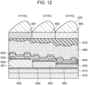
- a second embodiment differs from the first embodiment in FIG. 8A in that a light-shielding layer is provided.
- a light-shielding layer 920 is disposed on the planarizing layer 670, and another planarizing layer 930 is disposed on the light-shielding layer 920.
- the light-shielding layer 920 is formed between the pixels adjacent to each other.
- the light-shielding layer 920 enables color mixing of the pixels adjacent to each other to be inhibited. It suffices that the light-shielding layer 920 absorbs a wavelength component of a visible region of light that is emitted from the organic layer 640 that is the light-emitting layer.
- the light-shielding layer 920 may be a light-shielding layer that is obtained by stacking two or more kinds of color filters.
- the light-shielding layer 920 may be arranged so as to entirely cover the pixels or so as to partly cover the pixels.
- the light-shielding layer 920 does not need to completely shield light having a wavelength in the visible region, provided that 80% or more, preferably 90% or more of the light is shielded.
- a reflective structure may be disposed between the pixels adjacent to each other instead of the light-shielding layer 920. Also, with this structure, light is inhibited from entering the microlenses that are disposed in the pixels adjacent to each other, and color mixing of the pixels adjacent to each other can be inhibited.
- a third embodiment differs from the first embodiment in FIG. 8A in that optical adjustment layers are disposed below the organic layer, and reflection layers are disposed below the optical adjustment layers.
- the R-pixel includes an optical adjustment layer 951
- the G-pixel includes an optical adjustment layer 952
- the B-pixel includes an optical adjustment layer 953.
- Reflection layers 940 are disposed below the optical adjustment layers.
- the optical adjustment layers 951 to 953 have optimized optical film thicknesses depending on the wavelengths of the respective pixels.
- the directivity of light that is emitted from the RGB-pixels can be increased due to optical interference. Consequently, stray light toward a spherical microlens that is disposed between the pixels adjacent to each other can be inhibited. For this reason, useless luminous energy is eliminated, the use efficiency of light is improved, and color mixing due to stray light can be inhibited.
- the selectivity of the wavelength for every pixel is improved due to the optical interference, and the film thickness of each color filter can be decreased. For this reason, the distance between the organic layer and each microlens can be decreased, and stray light is inhibited from entering each microlens between the pixels adjacent to each other.
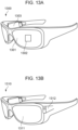
- Each display device can be used for a system that is capable of being worn as a wearable device such as smart glasses, a HMD, and a smart contact lens.
- An imaging display device that is used as an example of the application includes an imaging device that can carry out photoelectric conversion of the visible light and a display device that can emit the visible light.
- FIG. 13A illustrates glasses 1300 (smart glasses) that are used as an example of the application.
- An imaging device 1302 such as a CMOS sensor or a SPAD is disposed on a front surface of a lens 1301 of the glasses 1300.
- the display device according to one of the embodiments is disposed on a back surface of the lens 1301.
- the glasses 1300 also include a control device 1303.
- the control device 1303 functions as a power supply that supplies power to the imaging device 1302 and the display device according to the embodiment.
- the control device 1303 controls operation of the imaging device 1302 and the display device.
- the lens 1301 includes an optical system that focuses light onto the imaging device 1302.
- FIG. 13B illustrates glasses 1310 (smart glasses) that are used as an example of the application.
- the glasses 1310 include a control device 1312.
- the control device 1312 includes an imaging device that corresponds to the imaging device 1302 and a display device.
- a lens 1311 includes an optical system that projects light that is emitted from the display device and the imaging device in the control device 1312. An image is projected on the lens 1311.
- the control device 1312 functions as a power supply that supplies power to the imaging device and the display device and controls the operation of the imaging device and the display device.
- the arrangement of the pixels in each display device in a plan view is the delta arrangement of the honeycomb structure.
- the arrangement may be stripe arrangement, square arrangement, pen tile arrangement, or Bayer arrangement.
- RGB color filters are disposed in the respective pixels.
- organic layers that emit respective RGB colors may be disposed in the respective pixels.
- an organic LED is used as a display element.
- the display element can be an inorganic LED, a liquid-crystal element, or a reflective element, provided that the display element is a light-emitting element.
- a light-emitting element that uses quantum dots for a light-emitting layer or a light-emitting element that uses quantum dots for a color conversion layer are also acceptable.
- the materials of the quantum dots are particles of a material such as InP, CdS, PbS, ZnS, or CdSe. Core-shell quantum dots or perovskite quantum dots can be used.
- the asymmetrical microlens are used as the optical members.
- a display device that is capable of improving the quality of display can be provided.
Landscapes
- Physics & Mathematics (AREA)
- Geometry (AREA)
- Engineering & Computer Science (AREA)
- Microelectronics & Electronic Packaging (AREA)
- Optics & Photonics (AREA)
- Electroluminescent Light Sources (AREA)
- Optical Filters (AREA)
- Devices For Indicating Variable Information By Combining Individual Elements (AREA)
Applications Claiming Priority (1)
| Application Number | Priority Date | Filing Date | Title |
|---|---|---|---|
| JP2019130386A JP7353834B2 (ja) | 2019-07-12 | 2019-07-12 | 表示装置および表示システム |
Publications (2)
| Publication Number | Publication Date |
|---|---|
| EP3764399A1 EP3764399A1 (en) | 2021-01-13 |
| EP3764399B1 true EP3764399B1 (en) | 2023-11-01 |
Family
ID=71143524
Family Applications (1)
| Application Number | Title | Priority Date | Filing Date |
|---|---|---|---|
| EP20181964.6A Active EP3764399B1 (en) | 2019-07-12 | 2020-06-24 | Display device and display system |
Country Status (4)
| Country | Link |
|---|---|
| US (3) | US11665926B2 (enExample) |
| EP (1) | EP3764399B1 (enExample) |
| JP (1) | JP7353834B2 (enExample) |
| CN (1) | CN112216730B (enExample) |
Families Citing this family (18)
| Publication number | Priority date | Publication date | Assignee | Title |
|---|---|---|---|---|
| US11024651B2 (en) * | 2017-01-20 | 2021-06-01 | Sony Semiconductor Solutions Corporation | Display device and electronic device with microlens array and light emitting element substrates bonded by adhesive layer |
| US12279476B2 (en) * | 2019-07-12 | 2025-04-15 | Canon Kabushiki Kaisha | Light emitting device, exposure system, imaging display device, imaging device, electronic device, and lighting device |
| JP7353834B2 (ja) | 2019-07-12 | 2023-10-02 | キヤノン株式会社 | 表示装置および表示システム |
| US12484422B2 (en) * | 2020-12-18 | 2025-11-25 | Sony Semiconductor Solutions Corporation | Display apparatus and electronic device |
| CN117957943A (zh) * | 2021-08-18 | 2024-04-30 | 株式会社半导体能源研究所 | 显示装置及电子设备 |
| WO2023052892A1 (ja) * | 2021-09-29 | 2023-04-06 | 株式会社半導体エネルギー研究所 | 表示装置、および電子機器 |
| KR20230049191A (ko) * | 2021-10-05 | 2023-04-13 | 삼성디스플레이 주식회사 | 디스플레이 장치 및 그 제조방법 |
| WO2023070535A1 (zh) * | 2021-10-29 | 2023-05-04 | 京东方科技集团股份有限公司 | 显示装置、显示面板及其制造方法 |
| US20230378404A1 (en) * | 2021-11-23 | 2023-11-23 | Nanosys, Inc. | Light emitting device with improved radiation distribution and method of making thereof |
| JPWO2023106082A1 (enExample) * | 2021-12-10 | 2023-06-15 | ||
| JP7644743B2 (ja) * | 2021-12-13 | 2025-03-12 | キヤノン株式会社 | 発光装置、表示装置、撮像装置および電子機器 |
| KR20230094211A (ko) | 2021-12-20 | 2023-06-28 | 삼성디스플레이 주식회사 | 표시 장치 |
| CN114280793B (zh) * | 2021-12-30 | 2023-04-28 | 视涯科技股份有限公司 | 一种显示装置 |
| JP2023155685A (ja) * | 2022-04-11 | 2023-10-23 | Toppanホールディングス株式会社 | 表示装置 |
| KR20250046273A (ko) * | 2022-08-09 | 2025-04-02 | 소니 세미컨덕터 솔루션즈 가부시키가이샤 | 발광 장치 및 전자 기기 |
| CN118867095A (zh) * | 2023-04-28 | 2024-10-29 | 华为技术有限公司 | 显示模组和微显示器 |
| JP2025167026A (ja) * | 2024-04-25 | 2025-11-07 | Toppanホールディングス株式会社 | 表示デバイス及びその製造方法 |
| WO2025249180A1 (ja) * | 2024-05-30 | 2025-12-04 | ソニーセミコンダクタソリューションズ株式会社 | 表示装置 |
Family Cites Families (45)
| Publication number | Priority date | Publication date | Assignee | Title |
|---|---|---|---|---|
| JP4032918B2 (ja) * | 2002-10-24 | 2008-01-16 | ソニー株式会社 | 表示装置およびその製造方法 |
| JP2004347693A (ja) * | 2003-05-20 | 2004-12-09 | Seiko Epson Corp | マイクロレンズアレイ、空間光変調装置、プロジェクタ及びマイクロレンズアレイの製造方法 |
| JP2007253503A (ja) | 2006-03-24 | 2007-10-04 | Seiko Epson Corp | 電気光学装置および画像形成装置 |
| WO2008001241A2 (en) | 2006-06-14 | 2008-01-03 | Philips Intellectual Property & Standards Gmbh | Structured oled with micro optics for generating directed light |
| JP2007335723A (ja) | 2006-06-16 | 2007-12-27 | Fujifilm Corp | 固体撮像素子用マイクロレンズ及びその製造方法 |
| JP4737461B2 (ja) | 2008-07-09 | 2011-08-03 | セイコーエプソン株式会社 | 有機el露光ヘッドの製造方法 |
| JP5125935B2 (ja) * | 2008-09-22 | 2013-01-23 | 凸版印刷株式会社 | 光均一素子、光学シート、それを用いたバックライトユニットおよびディスプレイ装置 |
| JP5382304B2 (ja) | 2008-11-20 | 2014-01-08 | 伸和エクセル株式会社 | 照明装置 |
| JP2010135212A (ja) * | 2008-12-05 | 2010-06-17 | Panasonic Corp | 発光素子、それを用いた表示装置および照明装置、ならびに発光素子の製造方法 |
| JP2010160343A (ja) * | 2009-01-08 | 2010-07-22 | Seiko Epson Corp | プロジェクタ |
| JP4621779B2 (ja) | 2009-02-17 | 2011-01-26 | シャープ株式会社 | 照明デバイスおよび該照明デバイスを使用した照明装置 |
| JP2010272858A (ja) | 2009-04-22 | 2010-12-02 | Ccs Inc | 露光機用光源装置 |
| JP5471608B2 (ja) | 2009-11-02 | 2014-04-16 | ソニー株式会社 | 撮像装置付き画像表示装置 |
| KR101093037B1 (ko) * | 2009-12-02 | 2011-12-13 | 주식회사 래도 | 전광판용 픽셀 모듈 |
| WO2011086719A1 (ja) * | 2010-01-15 | 2011-07-21 | 凸版印刷株式会社 | 導光体、隠蔽構造体、これらを備えた照明装置、表示装置 |
| CN102906489B (zh) * | 2010-05-31 | 2015-05-06 | 大日本印刷株式会社 | 导光板、面光源装置以及显示装置 |
| JP2012059692A (ja) | 2010-08-09 | 2012-03-22 | Canon Inc | 有機エレクトロルミネッセンス表示装置 |
| JP2012134128A (ja) * | 2010-11-30 | 2012-07-12 | Canon Inc | 表示装置 |
| US9293734B2 (en) * | 2010-12-23 | 2016-03-22 | Universal Display Corporation | Light extraction block with curved surface |
| JP2012199231A (ja) * | 2011-03-04 | 2012-10-18 | Semiconductor Energy Lab Co Ltd | 表示装置 |
| JP2012248453A (ja) | 2011-05-30 | 2012-12-13 | Canon Inc | 表示装置 |
| JP2013114772A (ja) | 2011-11-25 | 2013-06-10 | Canon Inc | 表示装置 |
| JP2013251173A (ja) | 2012-06-01 | 2013-12-12 | Canon Inc | 表示装置の製造方法及び表示装置 |
| KR102039685B1 (ko) | 2013-04-17 | 2019-11-04 | 삼성디스플레이 주식회사 | 유기 발광 표시 장치 |
| JP5791664B2 (ja) * | 2013-06-28 | 2015-10-07 | キヤノン株式会社 | 光学素子アレイ、及び固体撮像装置 |
| JP2015187635A (ja) * | 2014-03-26 | 2015-10-29 | 株式会社Joled | 色変化部材、光装置、表示装置および電子機器 |
| KR102335812B1 (ko) | 2014-09-19 | 2021-12-09 | 삼성디스플레이 주식회사 | 유기발광 표시장치 |
| JP2016118675A (ja) * | 2014-12-22 | 2016-06-30 | キヤノン株式会社 | マイクロレンズ及びその製造方法 |
| JP2017079243A (ja) * | 2015-10-19 | 2017-04-27 | キヤノン株式会社 | 固体撮像装置及びカメラ |
| CN105182613A (zh) * | 2015-10-29 | 2015-12-23 | 京东方科技集团股份有限公司 | 一种光学结构、显示基板及显示器件 |
| KR102417142B1 (ko) * | 2015-11-11 | 2022-07-05 | 삼성디스플레이 주식회사 | 표시 장치 |
| KR102648410B1 (ko) * | 2016-03-11 | 2024-03-18 | 엘지디스플레이 주식회사 | 근안 표시 장치 |
| JP2017181831A (ja) * | 2016-03-31 | 2017-10-05 | ソニー株式会社 | 表示装置及び電子機器 |
| KR102457437B1 (ko) * | 2016-03-31 | 2022-10-24 | 소니그룹주식회사 | 표시 장치 및 전자 기기 |
| JP6270929B2 (ja) | 2016-07-12 | 2018-01-31 | 北明電気工業株式会社 | 照明装置 |
| US10459215B2 (en) | 2016-12-27 | 2019-10-29 | Kopin Corporation | Video display device |
| CN109427859B (zh) | 2017-08-31 | 2023-10-27 | 乐金显示有限公司 | 有机发光显示装置 |
| KR102328085B1 (ko) | 2017-11-30 | 2021-11-17 | 엘지디스플레이 주식회사 | 전계발광 표시장치 |
| JP7057147B2 (ja) * | 2018-01-31 | 2022-04-19 | ソニーセミコンダクタソリューションズ株式会社 | 発光素子及び表示装置 |
| WO2019159641A1 (ja) | 2018-02-16 | 2019-08-22 | ソニーセミコンダクタソリューションズ株式会社 | 表示装置およびその製造方法 |
| CN109216584B (zh) * | 2018-08-30 | 2020-09-01 | 武汉华星光电半导体显示技术有限公司 | 柔性oled显示面板 |
| DE112019005974T5 (de) | 2018-11-30 | 2021-09-09 | Sony Group Corporation | Anzeigevorrichtung |
| JP7006654B2 (ja) | 2019-05-09 | 2022-01-24 | セイコーエプソン株式会社 | 表示装置、および電子機器 |
| JP7353834B2 (ja) | 2019-07-12 | 2023-10-02 | キヤノン株式会社 | 表示装置および表示システム |
| CN112652728B (zh) | 2020-12-29 | 2022-11-25 | 视涯科技股份有限公司 | 一种显示面板及显示装置 |
-
2019
- 2019-07-12 JP JP2019130386A patent/JP7353834B2/ja active Active
-
2020
- 2020-06-24 EP EP20181964.6A patent/EP3764399B1/en active Active
- 2020-07-09 CN CN202010658167.2A patent/CN112216730B/zh active Active
- 2020-07-09 US US16/925,119 patent/US11665926B2/en active Active
-
2023
- 2023-03-17 US US18/185,909 patent/US12137578B2/en active Active
-
2024
- 2024-09-30 US US18/902,350 patent/US20250024703A1/en active Pending
Also Published As
| Publication number | Publication date |
|---|---|
| US12137578B2 (en) | 2024-11-05 |
| US20250024703A1 (en) | 2025-01-16 |
| JP2021015732A (ja) | 2021-02-12 |
| CN112216730B (zh) | 2024-09-06 |
| CN112216730A (zh) | 2021-01-12 |
| JP7353834B2 (ja) | 2023-10-02 |
| EP3764399A1 (en) | 2021-01-13 |
| US11665926B2 (en) | 2023-05-30 |
| US20210013453A1 (en) | 2021-01-14 |
| US20230232657A1 (en) | 2023-07-20 |
Similar Documents
| Publication | Publication Date | Title |
|---|---|---|
| EP3764399B1 (en) | Display device and display system | |
| US11967589B2 (en) | Systems and methods for multi-color LED pixel unit with horizontal light emission | |
| US20250266406A1 (en) | System and methods for multi-color led pixel unit | |
| KR102601422B1 (ko) | 발광 적층 구조체 및 이를 구비한 디스플레이 소자 | |
| US20210005583A1 (en) | Image display device | |
| CN212517209U (zh) | 显示面板和电子装置 | |
| US12243859B2 (en) | Image display element | |
| TWI766632B (zh) | 微型發光二極體顯示裝置 | |
| CN114284314A (zh) | 显示面板、电子装置以及显示面板的制作方法 | |
| TW202306216A (zh) | 微型發光二極體顯示裝置及其製造方法 | |
| JP2025038041A (ja) | 電子デバイス、表示装置、光電変換装置、電子機器、照明、および移動体 | |
| US20240421248A1 (en) | Systems and Methods for Multi-Color LED Pixel Unit | |
| WO2023100672A1 (ja) | 表示装置および電子機器 | |
| CN113066395A (zh) | 微型发光二极管显示设备 | |
| US20250105218A1 (en) | Display light engine and augmented reality display | |
| JP2025157122A (ja) | 発光装置、表示装置、光電変換装置および電子機器 | |
| KR20250163442A (ko) | 발광 다이오드, 발광 다이오드를 포함하는 표시 장치, 및 발광 다이오드의 제조 방법 | |
| KR20240040022A (ko) | 발광장치, 표시장치, 광전 변환장치, 및 전자기기 | |
| CN120897601A (zh) | Micro-LED显示芯片和制备方法 | |
| KR20250146938A (ko) | 발광장치, 표시장치, 광전 변환장치, 전자 기기, 및 화상 형성장치 | |
| CN119997713A (zh) | 一种Micro-LED微显示芯片及其制备方法 | |
| CN119234483A (zh) | 显示基板及其制备方法、显示装置 | |
| CN113594196A (zh) | 微型发光二极管显示装置及其制造方法 |
Legal Events
| Date | Code | Title | Description |
|---|---|---|---|
| PUAI | Public reference made under article 153(3) epc to a published international application that has entered the european phase |
Free format text: ORIGINAL CODE: 0009012 |
|
| STAA | Information on the status of an ep patent application or granted ep patent |
Free format text: STATUS: THE APPLICATION HAS BEEN PUBLISHED |
|
| AK | Designated contracting states |
Kind code of ref document: A1 Designated state(s): AL AT BE BG CH CY CZ DE DK EE ES FI FR GB GR HR HU IE IS IT LI LT LU LV MC MK MT NL NO PL PT RO RS SE SI SK SM TR |
|
| AX | Request for extension of the european patent |
Extension state: BA ME |
|
| STAA | Information on the status of an ep patent application or granted ep patent |
Free format text: STATUS: REQUEST FOR EXAMINATION WAS MADE |
|
| 17P | Request for examination filed |
Effective date: 20210713 |
|
| RBV | Designated contracting states (corrected) |
Designated state(s): AL AT BE BG CH CY CZ DE DK EE ES FI FR GB GR HR HU IE IS IT LI LT LU LV MC MK MT NL NO PL PT RO RS SE SI SK SM TR |
|
| GRAP | Despatch of communication of intention to grant a patent |
Free format text: ORIGINAL CODE: EPIDOSNIGR1 |
|
| STAA | Information on the status of an ep patent application or granted ep patent |
Free format text: STATUS: GRANT OF PATENT IS INTENDED |
|
| RIC1 | Information provided on ipc code assigned before grant |
Ipc: H01L 51/52 20060101ALI20221108BHEP Ipc: H01L 27/32 20060101AFI20221108BHEP |
|
| INTG | Intention to grant announced |
Effective date: 20221201 |
|
| RAP3 | Party data changed (applicant data changed or rights of an application transferred) |
Owner name: CANON KABUSHIKI KAISHA |
|
| GRAJ | Information related to disapproval of communication of intention to grant by the applicant or resumption of examination proceedings by the epo deleted |
Free format text: ORIGINAL CODE: EPIDOSDIGR1 |
|
| STAA | Information on the status of an ep patent application or granted ep patent |
Free format text: STATUS: REQUEST FOR EXAMINATION WAS MADE |
|
| INTC | Intention to grant announced (deleted) | ||
| REG | Reference to a national code |
Ref country code: DE Free format text: PREVIOUS MAIN CLASS: H01L0027320000 Ref country code: DE Ref legal event code: R079 Ref document number: 602020020112 Country of ref document: DE Free format text: PREVIOUS MAIN CLASS: H01L0027320000 Ipc: H10K0050858000 |
|
| GRAP | Despatch of communication of intention to grant a patent |
Free format text: ORIGINAL CODE: EPIDOSNIGR1 |
|
| STAA | Information on the status of an ep patent application or granted ep patent |
Free format text: STATUS: GRANT OF PATENT IS INTENDED |
|
| INTG | Intention to grant announced |
Effective date: 20230519 |
|
| RIC1 | Information provided on ipc code assigned before grant |
Ipc: H10K 59/121 20230101ALI20230508BHEP Ipc: H10K 50/858 20230101AFI20230508BHEP |
|
| GRAS | Grant fee paid |
Free format text: ORIGINAL CODE: EPIDOSNIGR3 |
|
| GRAA | (expected) grant |
Free format text: ORIGINAL CODE: 0009210 |
|
| STAA | Information on the status of an ep patent application or granted ep patent |
Free format text: STATUS: THE PATENT HAS BEEN GRANTED |
|
| AK | Designated contracting states |
Kind code of ref document: B1 Designated state(s): AL AT BE BG CH CY CZ DE DK EE ES FI FR GB GR HR HU IE IS IT LI LT LU LV MC MK MT NL NO PL PT RO RS SE SI SK SM TR |
|
| REG | Reference to a national code |
Ref country code: GB Ref legal event code: FG4D |
|
| REG | Reference to a national code |
Ref country code: CH Ref legal event code: EP |
|
| REG | Reference to a national code |
Ref country code: DE Ref legal event code: R096 Ref document number: 602020020112 Country of ref document: DE |
|
| REG | Reference to a national code |
Ref country code: IE Ref legal event code: FG4D |
|
| REG | Reference to a national code |
Ref country code: LT Ref legal event code: MG9D |
|
| REG | Reference to a national code |
Ref country code: NL Ref legal event code: MP Effective date: 20231101 |
|
| PG25 | Lapsed in a contracting state [announced via postgrant information from national office to epo] |
Ref country code: GR Free format text: LAPSE BECAUSE OF FAILURE TO SUBMIT A TRANSLATION OF THE DESCRIPTION OR TO PAY THE FEE WITHIN THE PRESCRIBED TIME-LIMIT Effective date: 20240202 |
|
| PG25 | Lapsed in a contracting state [announced via postgrant information from national office to epo] |
Ref country code: IS Free format text: LAPSE BECAUSE OF FAILURE TO SUBMIT A TRANSLATION OF THE DESCRIPTION OR TO PAY THE FEE WITHIN THE PRESCRIBED TIME-LIMIT Effective date: 20240301 |
|
| PG25 | Lapsed in a contracting state [announced via postgrant information from national office to epo] |
Ref country code: LT Free format text: LAPSE BECAUSE OF FAILURE TO SUBMIT A TRANSLATION OF THE DESCRIPTION OR TO PAY THE FEE WITHIN THE PRESCRIBED TIME-LIMIT Effective date: 20231101 |
|
| REG | Reference to a national code |
Ref country code: AT Ref legal event code: MK05 Ref document number: 1628743 Country of ref document: AT Kind code of ref document: T Effective date: 20231101 |
|
| PG25 | Lapsed in a contracting state [announced via postgrant information from national office to epo] |
Ref country code: NL Free format text: LAPSE BECAUSE OF FAILURE TO SUBMIT A TRANSLATION OF THE DESCRIPTION OR TO PAY THE FEE WITHIN THE PRESCRIBED TIME-LIMIT Effective date: 20231101 |
|
| PG25 | Lapsed in a contracting state [announced via postgrant information from national office to epo] |
Ref country code: AT Free format text: LAPSE BECAUSE OF FAILURE TO SUBMIT A TRANSLATION OF THE DESCRIPTION OR TO PAY THE FEE WITHIN THE PRESCRIBED TIME-LIMIT Effective date: 20231101 |
|
| PG25 | Lapsed in a contracting state [announced via postgrant information from national office to epo] |
Ref country code: ES Free format text: LAPSE BECAUSE OF FAILURE TO SUBMIT A TRANSLATION OF THE DESCRIPTION OR TO PAY THE FEE WITHIN THE PRESCRIBED TIME-LIMIT Effective date: 20231101 |
|
| PG25 | Lapsed in a contracting state [announced via postgrant information from national office to epo] |
Ref country code: NL Free format text: LAPSE BECAUSE OF FAILURE TO SUBMIT A TRANSLATION OF THE DESCRIPTION OR TO PAY THE FEE WITHIN THE PRESCRIBED TIME-LIMIT Effective date: 20231101 Ref country code: LT Free format text: LAPSE BECAUSE OF FAILURE TO SUBMIT A TRANSLATION OF THE DESCRIPTION OR TO PAY THE FEE WITHIN THE PRESCRIBED TIME-LIMIT Effective date: 20231101 Ref country code: IS Free format text: LAPSE BECAUSE OF FAILURE TO SUBMIT A TRANSLATION OF THE DESCRIPTION OR TO PAY THE FEE WITHIN THE PRESCRIBED TIME-LIMIT Effective date: 20240301 Ref country code: GR Free format text: LAPSE BECAUSE OF FAILURE TO SUBMIT A TRANSLATION OF THE DESCRIPTION OR TO PAY THE FEE WITHIN THE PRESCRIBED TIME-LIMIT Effective date: 20240202 Ref country code: ES Free format text: LAPSE BECAUSE OF FAILURE TO SUBMIT A TRANSLATION OF THE DESCRIPTION OR TO PAY THE FEE WITHIN THE PRESCRIBED TIME-LIMIT Effective date: 20231101 Ref country code: BG Free format text: LAPSE BECAUSE OF FAILURE TO SUBMIT A TRANSLATION OF THE DESCRIPTION OR TO PAY THE FEE WITHIN THE PRESCRIBED TIME-LIMIT Effective date: 20240201 Ref country code: AT Free format text: LAPSE BECAUSE OF FAILURE TO SUBMIT A TRANSLATION OF THE DESCRIPTION OR TO PAY THE FEE WITHIN THE PRESCRIBED TIME-LIMIT Effective date: 20231101 Ref country code: PT Free format text: LAPSE BECAUSE OF FAILURE TO SUBMIT A TRANSLATION OF THE DESCRIPTION OR TO PAY THE FEE WITHIN THE PRESCRIBED TIME-LIMIT Effective date: 20240301 |
|
| PG25 | Lapsed in a contracting state [announced via postgrant information from national office to epo] |
Ref country code: SE Free format text: LAPSE BECAUSE OF FAILURE TO SUBMIT A TRANSLATION OF THE DESCRIPTION OR TO PAY THE FEE WITHIN THE PRESCRIBED TIME-LIMIT Effective date: 20231101 Ref country code: RS Free format text: LAPSE BECAUSE OF FAILURE TO SUBMIT A TRANSLATION OF THE DESCRIPTION OR TO PAY THE FEE WITHIN THE PRESCRIBED TIME-LIMIT Effective date: 20231101 Ref country code: PL Free format text: LAPSE BECAUSE OF FAILURE TO SUBMIT A TRANSLATION OF THE DESCRIPTION OR TO PAY THE FEE WITHIN THE PRESCRIBED TIME-LIMIT Effective date: 20231101 Ref country code: NO Free format text: LAPSE BECAUSE OF FAILURE TO SUBMIT A TRANSLATION OF THE DESCRIPTION OR TO PAY THE FEE WITHIN THE PRESCRIBED TIME-LIMIT Effective date: 20240201 Ref country code: LV Free format text: LAPSE BECAUSE OF FAILURE TO SUBMIT A TRANSLATION OF THE DESCRIPTION OR TO PAY THE FEE WITHIN THE PRESCRIBED TIME-LIMIT Effective date: 20231101 Ref country code: HR Free format text: LAPSE BECAUSE OF FAILURE TO SUBMIT A TRANSLATION OF THE DESCRIPTION OR TO PAY THE FEE WITHIN THE PRESCRIBED TIME-LIMIT Effective date: 20231101 |
|
| PG25 | Lapsed in a contracting state [announced via postgrant information from national office to epo] |
Ref country code: DK Free format text: LAPSE BECAUSE OF FAILURE TO SUBMIT A TRANSLATION OF THE DESCRIPTION OR TO PAY THE FEE WITHIN THE PRESCRIBED TIME-LIMIT Effective date: 20231101 |
|
| PG25 | Lapsed in a contracting state [announced via postgrant information from national office to epo] |
Ref country code: CZ Free format text: LAPSE BECAUSE OF FAILURE TO SUBMIT A TRANSLATION OF THE DESCRIPTION OR TO PAY THE FEE WITHIN THE PRESCRIBED TIME-LIMIT Effective date: 20231101 |
|
| PG25 | Lapsed in a contracting state [announced via postgrant information from national office to epo] |
Ref country code: SK Free format text: LAPSE BECAUSE OF FAILURE TO SUBMIT A TRANSLATION OF THE DESCRIPTION OR TO PAY THE FEE WITHIN THE PRESCRIBED TIME-LIMIT Effective date: 20231101 |
|
| PG25 | Lapsed in a contracting state [announced via postgrant information from national office to epo] |
Ref country code: SM Free format text: LAPSE BECAUSE OF FAILURE TO SUBMIT A TRANSLATION OF THE DESCRIPTION OR TO PAY THE FEE WITHIN THE PRESCRIBED TIME-LIMIT Effective date: 20231101 Ref country code: SK Free format text: LAPSE BECAUSE OF FAILURE TO SUBMIT A TRANSLATION OF THE DESCRIPTION OR TO PAY THE FEE WITHIN THE PRESCRIBED TIME-LIMIT Effective date: 20231101 Ref country code: IT Free format text: LAPSE BECAUSE OF FAILURE TO SUBMIT A TRANSLATION OF THE DESCRIPTION OR TO PAY THE FEE WITHIN THE PRESCRIBED TIME-LIMIT Effective date: 20231101 Ref country code: EE Free format text: LAPSE BECAUSE OF FAILURE TO SUBMIT A TRANSLATION OF THE DESCRIPTION OR TO PAY THE FEE WITHIN THE PRESCRIBED TIME-LIMIT Effective date: 20231101 Ref country code: DK Free format text: LAPSE BECAUSE OF FAILURE TO SUBMIT A TRANSLATION OF THE DESCRIPTION OR TO PAY THE FEE WITHIN THE PRESCRIBED TIME-LIMIT Effective date: 20231101 Ref country code: CZ Free format text: LAPSE BECAUSE OF FAILURE TO SUBMIT A TRANSLATION OF THE DESCRIPTION OR TO PAY THE FEE WITHIN THE PRESCRIBED TIME-LIMIT Effective date: 20231101 |
|
| REG | Reference to a national code |
Ref country code: DE Ref legal event code: R097 Ref document number: 602020020112 Country of ref document: DE |
|
| PLBE | No opposition filed within time limit |
Free format text: ORIGINAL CODE: 0009261 |
|
| STAA | Information on the status of an ep patent application or granted ep patent |
Free format text: STATUS: NO OPPOSITION FILED WITHIN TIME LIMIT |
|
| 26N | No opposition filed |
Effective date: 20240802 |
|
| PG25 | Lapsed in a contracting state [announced via postgrant information from national office to epo] |
Ref country code: SI Free format text: LAPSE BECAUSE OF FAILURE TO SUBMIT A TRANSLATION OF THE DESCRIPTION OR TO PAY THE FEE WITHIN THE PRESCRIBED TIME-LIMIT Effective date: 20231101 |
|
| PG25 | Lapsed in a contracting state [announced via postgrant information from national office to epo] |
Ref country code: SI Free format text: LAPSE BECAUSE OF FAILURE TO SUBMIT A TRANSLATION OF THE DESCRIPTION OR TO PAY THE FEE WITHIN THE PRESCRIBED TIME-LIMIT Effective date: 20231101 |
|
| PG25 | Lapsed in a contracting state [announced via postgrant information from national office to epo] |
Ref country code: MC Free format text: LAPSE BECAUSE OF FAILURE TO SUBMIT A TRANSLATION OF THE DESCRIPTION OR TO PAY THE FEE WITHIN THE PRESCRIBED TIME-LIMIT Effective date: 20231101 |
|
| REG | Reference to a national code |
Ref country code: CH Ref legal event code: PL |
|
| PG25 | Lapsed in a contracting state [announced via postgrant information from national office to epo] |
Ref country code: LU Free format text: LAPSE BECAUSE OF NON-PAYMENT OF DUE FEES Effective date: 20240624 |
|
| GBPC | Gb: european patent ceased through non-payment of renewal fee |
Effective date: 20240624 |
|
| PG25 | Lapsed in a contracting state [announced via postgrant information from national office to epo] |
Ref country code: IE Free format text: LAPSE BECAUSE OF NON-PAYMENT OF DUE FEES Effective date: 20240624 |
|
| PG25 | Lapsed in a contracting state [announced via postgrant information from national office to epo] |
Ref country code: CH Free format text: LAPSE BECAUSE OF NON-PAYMENT OF DUE FEES Effective date: 20240630 Ref country code: BE Free format text: LAPSE BECAUSE OF NON-PAYMENT OF DUE FEES Effective date: 20240630 |
|
| PG25 | Lapsed in a contracting state [announced via postgrant information from national office to epo] |
Ref country code: FR Free format text: LAPSE BECAUSE OF NON-PAYMENT OF DUE FEES Effective date: 20240630 |
|
| PG25 | Lapsed in a contracting state [announced via postgrant information from national office to epo] |
Ref country code: GB Free format text: LAPSE BECAUSE OF NON-PAYMENT OF DUE FEES Effective date: 20240624 |
|
| REG | Reference to a national code |
Ref country code: BE Ref legal event code: MM Effective date: 20240630 |
|
| PGFP | Annual fee paid to national office [announced via postgrant information from national office to epo] |
Ref country code: DE Payment date: 20250520 Year of fee payment: 6 |
|
| PG25 | Lapsed in a contracting state [announced via postgrant information from national office to epo] |
Ref country code: FI Free format text: LAPSE BECAUSE OF FAILURE TO SUBMIT A TRANSLATION OF THE DESCRIPTION OR TO PAY THE FEE WITHIN THE PRESCRIBED TIME-LIMIT Effective date: 20231101 |
|
| PG25 | Lapsed in a contracting state [announced via postgrant information from national office to epo] |
Ref country code: RO Free format text: LAPSE BECAUSE OF FAILURE TO SUBMIT A TRANSLATION OF THE DESCRIPTION OR TO PAY THE FEE WITHIN THE PRESCRIBED TIME-LIMIT Effective date: 20231101 |
|
| PG25 | Lapsed in a contracting state [announced via postgrant information from national office to epo] |
Ref country code: CY Free format text: LAPSE BECAUSE OF FAILURE TO SUBMIT A TRANSLATION OF THE DESCRIPTION OR TO PAY THE FEE WITHIN THE PRESCRIBED TIME-LIMIT; INVALID AB INITIO Effective date: 20200624 |