EP3726719A1 - Stromwandler und stromwandlungsverfahren - Google Patents
Stromwandler und stromwandlungsverfahren Download PDFInfo
- Publication number
- EP3726719A1 EP3726719A1 EP19208167.7A EP19208167A EP3726719A1 EP 3726719 A1 EP3726719 A1 EP 3726719A1 EP 19208167 A EP19208167 A EP 19208167A EP 3726719 A1 EP3726719 A1 EP 3726719A1
- Authority
- EP
- European Patent Office
- Prior art keywords
- current source
- current
- inverter
- switch
- normally
- Prior art date
- Legal status (The legal status is an assumption and is not a legal conclusion. Google has not performed a legal analysis and makes no representation as to the accuracy of the status listed.)
- Ceased
Links
Images


Classifications
-
- H—ELECTRICITY
- H02—GENERATION; CONVERSION OR DISTRIBUTION OF ELECTRIC POWER
- H02M—APPARATUS FOR CONVERSION BETWEEN AC AND AC, BETWEEN AC AND DC, OR BETWEEN DC AND DC, AND FOR USE WITH MAINS OR SIMILAR POWER SUPPLY SYSTEMS; CONVERSION OF DC OR AC INPUT POWER INTO SURGE OUTPUT POWER; CONTROL OR REGULATION THEREOF
- H02M7/00—Conversion of ac power input into dc power output; Conversion of dc power input into ac power output
- H02M7/42—Conversion of dc power input into ac power output without possibility of reversal
- H02M7/44—Conversion of dc power input into ac power output without possibility of reversal by static converters
- H02M7/48—Conversion of dc power input into ac power output without possibility of reversal by static converters using discharge tubes with control electrode or semiconductor devices with control electrode
- H02M7/53—Conversion of dc power input into ac power output without possibility of reversal by static converters using discharge tubes with control electrode or semiconductor devices with control electrode using devices of a triode or transistor type requiring continuous application of a control signal
- H02M7/537—Conversion of dc power input into ac power output without possibility of reversal by static converters using discharge tubes with control electrode or semiconductor devices with control electrode using devices of a triode or transistor type requiring continuous application of a control signal using semiconductor devices only, e.g. single switched pulse inverters
- H02M7/5387—Conversion of dc power input into ac power output without possibility of reversal by static converters using discharge tubes with control electrode or semiconductor devices with control electrode using devices of a triode or transistor type requiring continuous application of a control signal using semiconductor devices only, e.g. single switched pulse inverters in a bridge configuration
- H02M7/53871—Conversion of dc power input into ac power output without possibility of reversal by static converters using discharge tubes with control electrode or semiconductor devices with control electrode using devices of a triode or transistor type requiring continuous application of a control signal using semiconductor devices only, e.g. single switched pulse inverters in a bridge configuration with automatic control of output voltage or current
-
- H—ELECTRICITY
- H02—GENERATION; CONVERSION OR DISTRIBUTION OF ELECTRIC POWER
- H02M—APPARATUS FOR CONVERSION BETWEEN AC AND AC, BETWEEN AC AND DC, OR BETWEEN DC AND DC, AND FOR USE WITH MAINS OR SIMILAR POWER SUPPLY SYSTEMS; CONVERSION OF DC OR AC INPUT POWER INTO SURGE OUTPUT POWER; CONTROL OR REGULATION THEREOF
- H02M1/00—Details of apparatus for conversion
- H02M1/32—Means for protecting converters other than automatic disconnection
-
- H—ELECTRICITY
- H02—GENERATION; CONVERSION OR DISTRIBUTION OF ELECTRIC POWER
- H02M—APPARATUS FOR CONVERSION BETWEEN AC AND AC, BETWEEN AC AND DC, OR BETWEEN DC AND DC, AND FOR USE WITH MAINS OR SIMILAR POWER SUPPLY SYSTEMS; CONVERSION OF DC OR AC INPUT POWER INTO SURGE OUTPUT POWER; CONTROL OR REGULATION THEREOF
- H02M3/00—Conversion of dc power input into dc power output
- H02M3/02—Conversion of dc power input into dc power output without intermediate conversion into ac
- H02M3/04—Conversion of dc power input into dc power output without intermediate conversion into ac by static converters
- H02M3/10—Conversion of dc power input into dc power output without intermediate conversion into ac by static converters using discharge tubes with control electrode or semiconductor devices with control electrode
- H02M3/145—Conversion of dc power input into dc power output without intermediate conversion into ac by static converters using discharge tubes with control electrode or semiconductor devices with control electrode using devices of a triode or transistor type requiring continuous application of a control signal
- H02M3/155—Conversion of dc power input into dc power output without intermediate conversion into ac by static converters using discharge tubes with control electrode or semiconductor devices with control electrode using devices of a triode or transistor type requiring continuous application of a control signal using semiconductor devices only
- H02M3/156—Conversion of dc power input into dc power output without intermediate conversion into ac by static converters using discharge tubes with control electrode or semiconductor devices with control electrode using devices of a triode or transistor type requiring continuous application of a control signal using semiconductor devices only with automatic control of output voltage or current, e.g. switching regulators
- H02M3/158—Conversion of dc power input into dc power output without intermediate conversion into ac by static converters using discharge tubes with control electrode or semiconductor devices with control electrode using devices of a triode or transistor type requiring continuous application of a control signal using semiconductor devices only with automatic control of output voltage or current, e.g. switching regulators including plural semiconductor devices as final control devices for a single load
-
- H—ELECTRICITY
- H02—GENERATION; CONVERSION OR DISTRIBUTION OF ELECTRIC POWER
- H02M—APPARATUS FOR CONVERSION BETWEEN AC AND AC, BETWEEN AC AND DC, OR BETWEEN DC AND DC, AND FOR USE WITH MAINS OR SIMILAR POWER SUPPLY SYSTEMS; CONVERSION OF DC OR AC INPUT POWER INTO SURGE OUTPUT POWER; CONTROL OR REGULATION THEREOF
- H02M7/00—Conversion of ac power input into dc power output; Conversion of dc power input into ac power output
- H02M7/42—Conversion of dc power input into ac power output without possibility of reversal
- H02M7/44—Conversion of dc power input into ac power output without possibility of reversal by static converters
- H02M7/48—Conversion of dc power input into ac power output without possibility of reversal by static converters using discharge tubes with control electrode or semiconductor devices with control electrode
- H02M7/483—Converters with outputs that each can have more than two voltages levels
- H02M7/487—Neutral point clamped inverters
-
- H—ELECTRICITY
- H02—GENERATION; CONVERSION OR DISTRIBUTION OF ELECTRIC POWER
- H02M—APPARATUS FOR CONVERSION BETWEEN AC AND AC, BETWEEN AC AND DC, OR BETWEEN DC AND DC, AND FOR USE WITH MAINS OR SIMILAR POWER SUPPLY SYSTEMS; CONVERSION OF DC OR AC INPUT POWER INTO SURGE OUTPUT POWER; CONTROL OR REGULATION THEREOF
- H02M1/00—Details of apparatus for conversion
- H02M1/0067—Converter structures employing plural converter units, other than for parallel operation of the units on a single load
- H02M1/007—Plural converter units in cascade
-
- H—ELECTRICITY
- H02—GENERATION; CONVERSION OR DISTRIBUTION OF ELECTRIC POWER
- H02M—APPARATUS FOR CONVERSION BETWEEN AC AND AC, BETWEEN AC AND DC, OR BETWEEN DC AND DC, AND FOR USE WITH MAINS OR SIMILAR POWER SUPPLY SYSTEMS; CONVERSION OF DC OR AC INPUT POWER INTO SURGE OUTPUT POWER; CONTROL OR REGULATION THEREOF
- H02M1/00—Details of apparatus for conversion
- H02M1/0083—Converters characterised by their input or output configuration
- H02M1/0087—Converters characterised by their input or output configuration adapted for receiving as input a current source
-
- H—ELECTRICITY
- H02—GENERATION; CONVERSION OR DISTRIBUTION OF ELECTRIC POWER
- H02M—APPARATUS FOR CONVERSION BETWEEN AC AND AC, BETWEEN AC AND DC, OR BETWEEN DC AND DC, AND FOR USE WITH MAINS OR SIMILAR POWER SUPPLY SYSTEMS; CONVERSION OF DC OR AC INPUT POWER INTO SURGE OUTPUT POWER; CONTROL OR REGULATION THEREOF
- H02M1/00—Details of apparatus for conversion
- H02M1/42—Circuits or arrangements for compensating for or adjusting power factor in converters or inverters
- H02M1/4208—Arrangements for improving power factor of AC input
- H02M1/4291—Arrangements for improving power factor of AC input by using a Buck converter to switch the input current
-
- Y—GENERAL TAGGING OF NEW TECHNOLOGICAL DEVELOPMENTS; GENERAL TAGGING OF CROSS-SECTIONAL TECHNOLOGIES SPANNING OVER SEVERAL SECTIONS OF THE IPC; TECHNICAL SUBJECTS COVERED BY FORMER USPC CROSS-REFERENCE ART COLLECTIONS [XRACs] AND DIGESTS
- Y02—TECHNOLOGIES OR APPLICATIONS FOR MITIGATION OR ADAPTATION AGAINST CLIMATE CHANGE
- Y02B—CLIMATE CHANGE MITIGATION TECHNOLOGIES RELATED TO BUILDINGS, e.g. HOUSING, HOUSE APPLIANCES OR RELATED END-USER APPLICATIONS
- Y02B70/00—Technologies for an efficient end-user side electric power management and consumption
- Y02B70/10—Technologies improving the efficiency by using switched-mode power supplies [SMPS], i.e. efficient power electronics conversion e.g. power factor correction or reduction of losses in power supplies or efficient standby modes
Definitions
- the at least two voltage levels may include an upper level +V dc /2 and a lower level -V dc /2 wherein V dc represents the voltage level of the DC voltage provided by the power source.
- V dc represents the voltage level of the DC voltage provided by the power source.
- Generating the output voltage may include alternatingly switching between the upper level for a first time period and the lower level for a second time period, wherein by suitably varying a ratio between the first time period and the second time period a polarity and a voltage level of the output voltage on average can be adjusted.
- a switching frequency in a voltage source inverter should not exceed several 10 kHz.
- such output filter may include one or more RC elements, wherein each RC element may include a resistor and a capacitor.
- the invention in particular relates to providing one or more free-wheeling paths in a current source inverter in case of loss of control signals or gate drive power by using a combination of normally-on and normally-off switches.
- a clamping network may be used to provide one or more free-wheeling paths in the current source inverter.
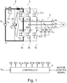
- Figure 1 shows one example of a power converter which includes a current source 2 and an inverter 3 connected to the power source 2, wherein this type of power converter may be referred to as current source inverter.
- the inverter 3 includes at least two half bridges, wherein the number of half bridges is dependent on the type of motor that is to be driven.
- the power converter is configured to provide three output currents i a , i b , i c in order to drive a 3-phase motor.
- Each half bridge is configured to provide one of the output currents i a , i b , i c so that in this example the inverter 3 includes three half bridges 3a, 3b, 3c.
- each of the half bridges 3a, 3b, 3c includes a high-side switch 31a, 31b, 31c and a low-side switch 32a, 32b, 32c.
- the high-side switch 31a, 31b, 31c and the low-side switch 32a, 32b, 32c of each half bridge 3a, 3b, 3c are connected in series between the intermediate nodes p, n.
- the tap a, b, c of each half bridge 3a, 3b, 3c is formed by a circuit node at which the respective high-side switch 31a, 31b, 31c and the respective low-side switch 32a, 32b, 32c are connected.
- drivers receive the control signals S31a, S31b, S31c, S32a, S32b, S32c and are configured to drive the high-side switches 31a, 31b, 31c and the low-side switches 32a, 32b, 32c based on the control signals S31a, S31b, S31c, S32a, S32b, S32c.
- reference number 3 denotes an arbitrary one or the plurality of the half bridges 3a, 3b, 3c.
- reference number 31 denotes an arbitrary one or the plurality of the high-side switches 31a, 31b, 31c
- reference number 32 denotes an arbitrary one or the plurality of the low-side switches 32a, 32b, 32c
- reference sign S31 denotes an arbitrary one or the plurality of the control signals S31a, S31b, S31c of the high-side switches 31a, 31b, 31c
- reference sign S32 denotes an arbitrary one or the plurality of the control signals S32a, S32b, S32c of the low-side switches 32a, 32b, 32c.
- the high-side switch 31 and the low-side switch 32 of at least one of the half bridges 3 are implemented as normally-on switches.
- a "normally-on switch” is an electronic switch that is in on-state (an electrically conducting state) when a drive signal received at a drive input is zero.
- a drive signal includes at least one of a drive voltage and a drive current.
- a drive signal of zero may occur intentionally when it is desired to switch on the respective switch by the controller 7.
- a drive signal of zero may also occur when a power supply of the controller 7 or the optional drivers (not shown) fails, or when a signal path between the controller 7 and a respective one of the switches 31, 32 is interrupted.
- the high-side switch 31 and the low-side switch 32 of at least one of the half bridges 3 as normally-on switches provides a current path in the inverter 3 for the source current i dc provided by the current source 2 when a failure occurs. If, for example, the switches 31a, 32a of the first half bridge 3a are implemented as normally-on switches the current i dc provided by the current source 2 can flow via the switches 31a, 32a of the first half bridge 3a in the inverter 3 back to the current source 2.
- the current source 2 may include an inductor 22 through which the source current i dc flows and a freewheeling element 23.
- the freewheeling element 23 in the current source 2 and the normally-on switches in the inverter 3 form a free-wheeling current path (that is illustrated in dashed lines in Figure 1 ), wherein this free-wheeling path allows the current through the inductor 22 to continue to flow when a failure occurs.
- switches of each of the half bridges 3a, 3b, 3c are implemented as normally-on switches.
- only one of the half bridges is implemented with normally-on switches.
- the normally-on switches are bidirectionally blocking GaN HEMTs (High Electron Mobility Transistors).
- a bidirectionally blocking GaN HEMT may include a series circuit of two unidirectionally blocking GaN HEMTs, wherein the two series connected HEMTs are driven by the same drive signal so that both HEMTs switch on or switch off at the same time.
- Bidirectionally blocking GaN HEMTs are commonly known, so that no further explanations are required in this regard.
- the topology according to Figure 1 uses bidirectional switches to create a bridge allowing recuperation of the rotating energy of the machine (the motor M) or its load respectively with only two switches between the current source 2 and the motor M.
- the current can be modulated in the form of a three-phase rectified sinusoidal waveform.
- the amplitude can be regulated in such a way that the current exactly matches the power required by the motor. With such a regulation scheme a very simple and effective modulation scheme can be used. If the current is too high part of the current can be bypassed from the motor M by short-circuiting one bridge leg, that is, by switching on the high-side switch 31 and the low-side switch 32 of one half-bridge.
- switches 31, 32 of at least one of the half-bridges 3 as normally-on switches provides one free-wheeling path for the current i dc provided by the current source 2 without short circuiting an output filter (that is explained herein further below) nor input 11, 12.
- normally-on switches in particular in combination with normally-off switches, features a high degree of fail-safe operation and will not lead to destruction of switches in case of e.g. loss of gate drive power or loss of control signals S31, S32.
- a combination of normally-on and normally-off switches may be used in a currents source inverter that is used in a motor drive. This, however, is only an example. A current source inverter of this type may be used in other cases as well.
- the inverter 3 shown in Figure 1 is a 3-phase inverter, which is an inverter configured to provide three output voltages v a , v b , v c and three output currents i a , i b , i c . Consequently, the motor M is a 3-phase motor.
- the inverter could also be implemented as a 2-phase inverter. An example of a 2-phase inverter is explained herein further below.
- an output filter 4 may be connected between the output nodes 5a, 5b, 5c and a ground node m.
- this filter 4 is a capacitive filter that includes a plurality of capacitors 4a, 4b, 4c, wherein each of these capacitors 4a, 4b, 4c is connected between the ground node m and a respective one of the output nodes 5a, 5b, 5c, wherein the ground node m may be different from each of the input nodes 11, 12.
- the high-side switch 31 and the low-side switch 32 of only one of the half-bridges 3 are implemented as normally-on switches while the high-side switch 31 and the low-side switch 32 of the remainder of the half-bridges 3 are normally-off switches.
- a failure occurs, a short circuit between the filter capacitances 4a, 4b, 4c of the output filter 4 can be prevented.
- a current source topology in comparison to the well-known voltage source converter is that the motor M is fed by a continuous voltage with currents i a , i b , i c being controlled and re-directed to the three windings of the motor M.
- the current waveforms ideally sinusoidal with varying frequency, can be pre-shaped by the current source 2 in such a way that the resulting waveform represents a rectified three-phase sinusoidal signal.
- This type of modulation scheme is disclosed in Swiss patent application no. 00127/19 (applicant: ETH Zürich, applicant's reference no. P4688 CH). This modulation scheme allows to refrain from PWM switching at intervals of the most positive and most negative phase currents and hence increases efficiency while lowering control complexity simultaneously. This is explained in the following.
- the inverter 3 is configured to generate alternating output currents i a , i b , i c based on the source current i dc . More specifically, the inverter 3 is configured to generate three sinusoidal output currents i a , i b , i c each having a predefined frequency and amplitude, wherein a phase shift between these output currents i a , i b , i c is essentially 120°.
- the current i a at the first output node 5a is referred to as first output current
- the current i b at the second output node 5b is referred to as second output current
- the current i c at the third output node 5c is referred to as third output current.
- Each of these currents i a , i b , i c can have one of two different current directions, a first direction and an opposite second direction.
- the first direction equals the direction illustrated by the arrows in Figure 1 and that the second direction is opposite to the direction indicated by the arrows in Figure 1 .
- An output current having the first direction is referred to as "positive output current” in the following
- an output current having the second direction is referred to as "negative output current” in the following.
- the output current the absolute value of which is given by the absolute value of the sum of the two other output currents is referred to as maximum output current. Equivalently, the one of the outputs that receives the maximum output current is referred to as maximum current output.
- the second output current i b is the maximum output current and the second output 5b is the maximum current output; in the fifth sector S5, for example, the negative first output current i a is the maximum output current and the first output 5a is the maximum current output.
- the current source 2 is configured to generate the source current i dc such that the source current in each of the six different sectors S1-S6 equals the absolute value of the respective maximum output current.
- the current source 2 and the inverter 3 may be controlled by a controller 7.
- This controller 7 may receive a motor control signal, wherein the motor control signal represents desired signal waveforms of the three output currents i a , i b , i c .
- the motor control signal represents the frequency and the amplitude of the three output currents i a , i b , i c .
- the controller 7 is configured to control the current source 2 such that the source current i dc is in accordance with the desired output currents i a , i b , i c represented by the motor control signal.
- the current source 2 may be implemented with a buck converter topology.
- the current source 2 includes a series circuit with an electronic switch 21 and an inductor 22 connected between one of the input nodes 11, 12 and one of the intermediate nodes p, n.
- the current source 2 includes a freewheeling element 23 that is connected between the other one of the intermediate circuit nodes p, n and a circuit node located between the electronic switch 21 and the inductor 22.
- the electronic switch 21 may be implemented as a MOSFET, in particular an n-type enhancement MOSFET. This, however, is only an example. Any other type of electronic switch may be used as well.
- the electronic switch 21 and the freewheeling element 23 form a half-bridge connected to the input 11, 12.
- the electronic switch 21 repeatedly switches on in order to connect the inductor 22 to the voltage source 6, wherein in those time periods in which the electronic switch 21 is switched off the free-wheeling element 23 takes over the current i dc through the inductor 22.
- the freewheeling element 23 may be implemented as an active freewheeling element (which may also be referred to as synchronous rectifier).
- the free-wheeling element 23 is implemented as a MOSFET, in particular an n-type enhancement MOSFET. This MOSFET is connected between the intermediate circuit node n and the inductor 22 such that an integrated body diode of the MOSFET 23 conducts the inductor current i dc when the MOSFET 23 is switched off.
- the controller 7 is configured to regulate the source current i dc (which equals the current through the inductor 22) in such a way that the source current i dc is in accordance with a current as defined by the motor control signal.
- the controller 7 receives a source current signal Side that represents the source current i dc .
- This current signal Side may be provided by a current sensor (not shown) that is configured to sense the source current i dc and provide the current signal S idc such that it represents the source current i dc .
- the current signal S idc is proportional to the source current i dc .
- a current sensor of this type is commonly known, so that no further explanation is required in this regard.
- the current signal S idc represents the actual value of the source current i dc and the motor control signal represents a desired value of the source current i dc .
- the controller 7 using control signal S21 operates the electronic switch 21 in a PWM fashion such that the source current i dc is essentially in accordance with the current defined by the motor control signal.
- Operating the electronic switch 21 in the PWM fashion includes switching on the electronic switch 21 for an on-period and switching off the electronic switch for an off-period in each of a plurality of successive drive cycles. These drive cycles may have the same duration (so that the electronic switch 21 is switched on at a fixed frequency).
- a duty cycle of the PWM operation of the electronic switch 21 is varied by the controller 7 in order to regulate the source current i dc .
- the freewheeling element 23, using control signal S23, is operated in a complementary fashion so that each time the electronic switch 21 is in an on-state the freewheeling element 23 is in an off-state, and vice versa.
- Operating a buck converter of the type shown in Figure 1 as a current source is basically known, so that no further explanation is required in this regard.
- the inverter 3 is configured to generate the output currents i a , i b , i c based on the source current i dc provided by the current source 2. This is explained in the following with reference to Figure 2 . It should be noted that Figure 2 schematically illustrates the individual currents and signals over one period of the sinusoidal output currents i a , i b , i c . In the time domain, the frequency and the amplitude of these output currents i a , i b , i c may vary as governed by the motor control signal.
- Figure 2 schematically illustrates the source current i dc , the output currents i a , i b , i c and the control signals S31a, S31b, S31c, S32a, S32b, S32c generated by the controller 7 and received by the high-side switches 31a, 31b, 31c and the low-side switches 32a, 32b, 32c.
- Each of the control signals S31, S32 may have two different signal levels, an on-level that is configured to switch on the respective switch 31, 32 and an off-level that is configured to switch off the respective switch 31, 32. It should be noted that Figure 2 only serves to illustrate whether it is desired to switch on or switch off a respective switch and does not necessarily illustrate the physical signal levels of the control signals S31, S32.
- a higher one of the two signal levels represents an on-level and a lower one of the two signal levels represents an off-level.
- hatched sections of the drive signals S31, S32 represent those sectors in which the respective switch is operated in a PWM fashion. (The duration of one drive cycle in the PWM mode is significantly shorter than the duration of each of the six sectors S1-S6, so that in the PWM mode the respective switch is switched on and off many times.)
- the source current i dc is generated such that it equals the absolute value of the maximum current in each of the six different sectors S1-S6.
- the one of the half bridges 3 that has its tap connected to the maximum output has one of its high-side switch 31 and its low-side switch 32 switched on throughout the respective sector.
- the second output current i b is the maximum output current, wherein this current is a negative current in this sector.
- the low-side switch 32b of the second half bridge 2b is switched on throughout the first sector S1.
- the first output current i a and the third output current i c are positive in the first sector so that the high-side switches 31a, 31c of the first and third half bridge 2a, 2c are operated in a PWM fashion throughout the first sector.
- a duty cycle of an operation of these high-side switches 31a, 31c varies throughout the first sector 1 in order to regulate these currents i a , i c .
- a switch in two of the half-bridges 3 is operated in a PWM fashion (while the other switch in these two half-bridges is switched off).
- the current at the tap of these two half-bridges is a PWM current, wherein the capacitive output filter 4 filters the PWM currents such that continuous output currents i a , i b , i c are obtained.
- the current can be modulated in classic PWM mode which is commonly known.
- the current source 2 provides a source current i dc which is essentially constant over one period of the output currents i a , i b , i c and has an absolute value that equals a maximum of the absolute value of the maximum output current in each of the six sectors S1-S6. That is, the source current may have a constant current level equal to the maxima of the source current i dc illustrated in Figure 2 , or higher.
- the one of the half-bridges that provides the maximum output current in each sector does not have one of the high-side switch 31 and the low-side 32 switched on throughout the respective one of the sectors S1-S6, but operates in a PWM mode such that alternatingly an output current is provided at the respective tap a, b, c and the respective tap a, b, c is bypassed.
- the second output current i b is the maximum output current and is negative.
- the low-side switch 32a is switched (output current mode) on and both the high-side switch 31a and the low-side switch 32a are switched on (bypass mode).
- FIG. 1 shows a case with the high side (control switch) 21 of the buck converter 2 being turned on and current free-wheeling through leg a.
- the current can free-wheel through the first half-bridge 3a (bridge leg "a") if these switches 31a, 32a are normally-on devices.
- the current loop is closed through the body diode of the freewheeling element 23.
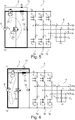
- Figure 3 shows a modification of the power converter shown in Figure 1 .
- the inverter 3 includes an H4 configuration with two half bridges 2a, 2b.
- This inverter 3 is configured to drive a single phase motor.
- Output currents i a , i b of this inverter have a phase shift of 180°.
- a first one 2a of the two half bridges 2a, 2b includes normally-on switches, while the other one 2b of the two half bridges 2a, 2b includes normally-off switches.
- Figure 4 illustrates another modification of the power converter shown in Figure 1 .
- the current source 2 is configured to receive a 3-phase sinusoidal input voltage at an input 13, 14, 15 instead of a DC voltage as illustrated in Figure 1 .
- the current source 2 includes three half bridges 2d, 2e, 2f, wherein each of these half bridges 2d, 2e, 2f includes a respective tap d, e, f connected to a respective one of the input nodes 13, 14, 15, wherein each of these input nodes 13, 14, 15 is coupled to one phase of a 3-phase voltage source (not shown in Figure 4 ).
- a high-side switch 21d, 21e, 21f of each half-bridge 2d, 2e, 2f is connected between the inductor 22 and a respective one of the taps d, e, f, and a low-side switch 23d, 23e, 23f is connected between the respective tap d, e, f and the second intermediate node n.
- the half bridges 2d, 2e, 2f of the current source 2 are driven by the controller 7 (not shown in Figure 4 ) dependent on the motor control signal such that the source current i dc provided by the current source 2 is in accordance with the motor control signal. More specifically, the controller 7 is configured to generate drive signals received by the electronic switches of the half-bridges 2d, 2e, 2f. These drive signals are PWM signals, wherein the controller 7 is configured to control a duty cycle of these PWM signals such that the source current i dc is in accordance with the motor control signal.
- the switches of at least one of the half-bridges 2d, 2e, 2f of the current source 3 are implemented as normally-on switches.
- the switches of one of the half-bridges 2d, 2e, 2f of the current source 2 are normally-on switches and the switches of the other two of the half-bridges 2d, 2e, 2f are normally-off switches.
- the one of the half-bridges 2d, 2e, 2f of the current source 2 that includes the normally-on switches and the one of the half-bridges 3a, 3b, 3c of the inverter 3 that includes the normally-on switches provide a freewheeling path for the source current i dc when a failure occurs.
- Figures 5 and 6 illustrate another example of the power converter.
- the high-side switches and the low-side switches 31, 32 of each half-bridge 3a, 3b, 3c may be implemented as normally-off switches. However, it is also possible to implement these switches 31, 32 as normally-on switches.
- a freewheeling path for the current i dc provided by the current source 3 is provided by a diode clamping network that includes a first diode 71 connected in parallel with the series circuit including the switch 21 and the inductor 22 and a second diode connected in parallel with the half-bridges 3a, 3b, 3c.
- a freewheeling element 73 is connected only in parallel with the inductor 22.
- the freewheeling element 73 is a normally-on switch.
- the normally-on switch is a bidirectionally blocking GaN HEMT.
Priority Applications (1)
| Application Number | Priority Date | Filing Date | Title |
|---|---|---|---|
| US16/848,104 US11728746B2 (en) | 2019-04-15 | 2020-04-14 | Current source inverter and method of operating a current source inverter |
Applications Claiming Priority (1)
| Application Number | Priority Date | Filing Date | Title |
|---|---|---|---|
| DE102019109927 | 2019-04-15 |
Publications (1)
| Publication Number | Publication Date |
|---|---|
| EP3726719A1 true EP3726719A1 (de) | 2020-10-21 |
Family
ID=68617988
Family Applications (1)
| Application Number | Title | Priority Date | Filing Date |
|---|---|---|---|
| EP19208167.7A Ceased EP3726719A1 (de) | 2019-04-15 | 2019-11-08 | Stromwandler und stromwandlungsverfahren |
Country Status (2)
| Country | Link |
|---|---|
| US (1) | US11728746B2 (de) |
| EP (1) | EP3726719A1 (de) |
Cited By (1)
| Publication number | Priority date | Publication date | Assignee | Title |
|---|---|---|---|---|
| WO2023229876A1 (en) * | 2022-05-23 | 2023-11-30 | Panduit Corp. | System's, apparatuses, and methods for pulse shaping in high voltage power systems |
Citations (7)
| Publication number | Priority date | Publication date | Assignee | Title |
|---|---|---|---|---|
| US20100141188A1 (en) * | 2007-04-27 | 2010-06-10 | Meidensha Corporation | Motor drive |
| EP2299583A1 (de) * | 2008-06-27 | 2011-03-23 | Daikin Industries, Ltd. | Umsetzungseinrichtung für elektrischen strom |
| US20110157948A1 (en) * | 2009-12-28 | 2011-06-30 | Sanken Electric Co., Ltd. | Current source inverter |
| US20120112671A1 (en) * | 2009-07-08 | 2012-05-10 | Meidensha Corporation | Power-consumption calculating method of motor driving device, and control method of motor driving device using the power-consumption calculating method |
| US20140015592A1 (en) * | 2012-07-11 | 2014-01-16 | Infineon Technologies Dresden Gmbh | Integrated circuit with at least two switches |
| CN107769559A (zh) * | 2017-11-15 | 2018-03-06 | 天津津航计算技术研究所 | 一种可以实现快速换向的双向dc/dc变换电路 |
| WO2018168328A1 (ja) * | 2017-03-14 | 2018-09-20 | 日本電産株式会社 | パワー半導体スイッチング素子のダメージ予測装置及びダメージ予測方法、ac-dcコンバータ、dc-dcコンバータ |
Family Cites Families (63)
| Publication number | Priority date | Publication date | Assignee | Title |
|---|---|---|---|---|
| US4833584A (en) * | 1987-10-16 | 1989-05-23 | Wisconsin Alumni Research Foundation | Quasi-resonant current mode static power conversion method and apparatus |
| US6075328A (en) * | 1996-10-18 | 2000-06-13 | Hitachi, Ltd. | PWM/PAM control mode switching type motor control apparatus, and motor drive and air-conditioner using the same |
| US5764024A (en) * | 1997-04-07 | 1998-06-09 | Motorola, Inc. | Pulse width modulator (PWM) system with low cost dead time distortion correction |
| US6271651B1 (en) * | 2000-04-20 | 2001-08-07 | Volterra Semiconductor Corporation | Inductor shorting switch for a switching voltage regulator |
| EP1414145B1 (de) * | 2001-08-02 | 2019-12-25 | Toyota Jidosha Kabushiki Kaisha | Steuervorrichtung für einen motorantrieb |
| DE60239764D1 (de) * | 2001-12-26 | 2011-05-26 | Toyota Motor Co Ltd | Elektrische lastvorrichtung, steuerverfahren für eine elektrische last und computerlesbares aufzeichnungsmedium mit einem aufgezeichneten programm, durch das ein computer eine elektrische last steuern kann |
| JP2004015892A (ja) * | 2002-06-05 | 2004-01-15 | Toshiba Corp | インバータの制御装置及び電気自動車 |
| US7274576B1 (en) * | 2006-03-01 | 2007-09-25 | Rockwell Automation Technologies, Inc. | Power converter with reduced common mode voltage |
| JP2007288992A (ja) * | 2006-03-20 | 2007-11-01 | Hitachi Ltd | 半導体回路 |
| DE102006016502A1 (de) * | 2006-04-07 | 2007-10-18 | Siemens Ag | Wechselrichter |
| US9397580B1 (en) * | 2006-06-06 | 2016-07-19 | Ideal Power, Inc. | Dual link power converter |
| US8514601B2 (en) * | 2009-08-17 | 2013-08-20 | Ideal Power Converters, Inc. | Power conversion with added pseudo-phase |
| US9678519B1 (en) * | 2006-06-06 | 2017-06-13 | Ideal Power, Inc. | Voltage control modes for microgrid applications |
| US7778045B2 (en) * | 2006-06-06 | 2010-08-17 | Ideal Power Converters, Inc. | Universal power conversion methods |
| JP4082438B2 (ja) * | 2006-08-30 | 2008-04-30 | ダイキン工業株式会社 | 電流制御形電力変換装置 |
| JP4988374B2 (ja) * | 2007-02-15 | 2012-08-01 | 三洋電機株式会社 | モータ制御装置 |
| JP4329855B2 (ja) * | 2007-10-09 | 2009-09-09 | トヨタ自動車株式会社 | 交流モータの制御装置および交流モータの制御方法 |
| JP5433214B2 (ja) * | 2007-12-07 | 2014-03-05 | パナソニック株式会社 | モータ駆動回路 |
| FR2925241B1 (fr) * | 2007-12-17 | 2010-01-08 | Schneider Electric Ind Sas | Generateur de tension alternative dote d'un dispositif de limitation de courant |
| JP5304192B2 (ja) * | 2008-03-28 | 2013-10-02 | ダイキン工業株式会社 | 電力変換装置 |
| WO2009157097A1 (ja) * | 2008-06-27 | 2009-12-30 | 国立大学法人 東京工業大学 | Pmモータ駆動電源装置 |
| JP4858597B2 (ja) * | 2008-11-28 | 2012-01-18 | 株式会社デンソー | 回転機の制御装置及びその製造方法 |
| JP5407322B2 (ja) * | 2008-12-22 | 2014-02-05 | トヨタ自動車株式会社 | 交流電動機の制御システム |
| JP5381361B2 (ja) * | 2009-06-11 | 2014-01-08 | 株式会社豊田自動織機 | インバータ装置 |
| JP5461899B2 (ja) * | 2009-06-26 | 2014-04-02 | 株式会社東芝 | 電力変換装置 |
| BRPI1011551A2 (pt) * | 2009-06-29 | 2016-03-29 | Ideal Power Converters Inc | dispositivos, métodos e sistemas de transferência de energia com reatância de transferência de energia com desvio de comutador de barra de segurança elétrica |
| BR112012003612A2 (pt) * | 2009-08-17 | 2017-05-23 | Ideal Power Converters Inc | conversão de força com pseudofase acrescentada |
| KR101031217B1 (ko) * | 2009-10-21 | 2011-04-27 | 주식회사 오리엔트전자 | 고정 시비율로 동작하는 llc 공진 컨버터를 사용한 2단 방식 절연형 양방향 dc/dc 전력변환기 |
| JP2011097787A (ja) * | 2009-10-30 | 2011-05-12 | Sanyo Electric Co Ltd | 系統連系インバータ装置及び系統連系システム |
| KR101106413B1 (ko) * | 2010-06-14 | 2012-01-17 | 삼성에스디아이 주식회사 | 에너지 저장 시스템의 인버터 |
| GB201010443D0 (en) * | 2010-06-22 | 2010-08-04 | Aeristech Ltd | Controller |
| JP5292363B2 (ja) * | 2010-06-30 | 2013-09-18 | 株式会社日立製作所 | 交流電動機の制御装置及び制御方法 |
| JP2012029429A (ja) * | 2010-07-22 | 2012-02-09 | Fuji Electric Co Ltd | 3レベル電力変換装置 |
| EP2590311A4 (de) * | 2010-09-29 | 2014-04-23 | Panasonic Corp | Stromwandlungsvorrichtung |
| US8476859B2 (en) * | 2010-09-30 | 2013-07-02 | Rockwell Automation Technologies, Inc. | DC power for SGCT devices using a high frequency current loop with multiple current transformers |
| US9013111B2 (en) * | 2010-10-12 | 2015-04-21 | National Cheng Kung University | Full-bridge electronic ballast having simplified continuous-conduction-mode charge pump PFC circuit |
| JP5352570B2 (ja) * | 2010-12-13 | 2013-11-27 | 株式会社日立製作所 | 回転機の制御装置,回転機系,車両,電気自動車または発電システム |
| WO2012105264A1 (ja) * | 2011-02-04 | 2012-08-09 | パナソニック株式会社 | 電源開閉装置およびそれを備える電源システム |
| WO2014040170A1 (en) * | 2012-09-14 | 2014-03-20 | Queen's University At Kingston | Interleaved resonant converter |
| JP6024601B2 (ja) * | 2012-11-26 | 2016-11-16 | 株式会社豊田自動織機 | インバータの暖機制御装置 |
| JP5831444B2 (ja) * | 2012-12-26 | 2015-12-09 | 株式会社デンソー | 回転機の制御装置 |
| US9647568B1 (en) * | 2013-02-15 | 2017-05-09 | Ideal Power, Inc. | Bi-directional multi-port applications |
| GB2522362B (en) * | 2013-06-24 | 2015-11-11 | Ideal Power Inc | Systems, circuits, devices, and methods with bidirectional bipolar transistors |
| EP2858195B1 (de) * | 2013-10-07 | 2017-08-02 | ABB Technology Oy | Wandlerschaltung |
| US9800167B2 (en) * | 2014-02-07 | 2017-10-24 | Abb Schweiz Ag | Multi-phase AC/AC step-down converter for distribution systems |
| US9680376B2 (en) * | 2014-02-28 | 2017-06-13 | Cree, Inc. | Power conversion electronics having conversion and inverter circuitry |
| JP5958494B2 (ja) * | 2014-04-23 | 2016-08-02 | 株式会社デンソー | スイッチング制御装置 |
| TWI509972B (zh) * | 2014-06-25 | 2015-11-21 | Delta Electronics Inc | 柔性切換式雙向電源轉換器及其操作方法 |
| EP3180849B1 (de) * | 2014-08-13 | 2021-11-10 | INESC TEC - Instituto de Engenharia de Sistemas e Computadores, Tecnologia e Ciência | Ac/dc umrichter mit 3 zu einer phase matrix umrichter, vollbrücken ac/dc umrichter und hf trafo |
| US9344021B2 (en) * | 2014-09-11 | 2016-05-17 | GM Global Technology Operations LLC | Inverter circuit for an electric machine |
| US9419549B2 (en) * | 2014-11-14 | 2016-08-16 | GM Global Technology Operations LLC | Method and apparatus for controlling an electric machine in a six-step mode |
| US10027112B2 (en) * | 2015-06-24 | 2018-07-17 | Eaton Intelligent Power Limited | High voltage power supplies using serially coupled current source rectifiers and methods of operating the same |
| US10432129B2 (en) * | 2015-10-13 | 2019-10-01 | Mitsubishi Electric Corporation | AC rotary machine control device and electric power steering device |
| JP6330822B2 (ja) * | 2016-01-14 | 2018-05-30 | トヨタ自動車株式会社 | 燃料電池システム及びその制御方法 |
| EP3316463A1 (de) * | 2016-10-27 | 2018-05-02 | Siemens Aktiengesellschaft | Ändern eines schaltzustands einer schalt-halbbrücke |
| JP6702209B2 (ja) * | 2017-01-26 | 2020-05-27 | 株式会社デンソー | 電力変換装置 |
| JP2018137952A (ja) * | 2017-02-23 | 2018-08-30 | 株式会社ジェイテクト | インバータ回路、モータ制御装置及びパワーステアリング装置 |
| US10574136B2 (en) * | 2018-04-17 | 2020-02-25 | Abb Schweiz Ag | Methods and systems for controlling current source rectifiers |
| EP3696966B1 (de) * | 2017-10-13 | 2024-03-27 | Nabtesco Corporation | Wechselstrom-wechselstrom-umrichter |
| JP2019092292A (ja) * | 2017-11-14 | 2019-06-13 | 株式会社ジェイテクト | 電力変換装置 |
| JP6954205B2 (ja) * | 2018-03-28 | 2021-10-27 | トヨタ自動車株式会社 | 電力変換器 |
| US10826424B2 (en) * | 2018-07-10 | 2020-11-03 | GM Global Technology Operations LLC | Method and apparatus for controlling a cascaded inverter circuit and an electric machine |
| FR3101211B1 (fr) * | 2019-09-24 | 2021-11-05 | Commissariat Energie Atomique | Onduleur à source de courant muni d’un circuit de protection |
-
2019
- 2019-11-08 EP EP19208167.7A patent/EP3726719A1/de not_active Ceased
-
2020
- 2020-04-14 US US16/848,104 patent/US11728746B2/en active Active
Patent Citations (7)
| Publication number | Priority date | Publication date | Assignee | Title |
|---|---|---|---|---|
| US20100141188A1 (en) * | 2007-04-27 | 2010-06-10 | Meidensha Corporation | Motor drive |
| EP2299583A1 (de) * | 2008-06-27 | 2011-03-23 | Daikin Industries, Ltd. | Umsetzungseinrichtung für elektrischen strom |
| US20120112671A1 (en) * | 2009-07-08 | 2012-05-10 | Meidensha Corporation | Power-consumption calculating method of motor driving device, and control method of motor driving device using the power-consumption calculating method |
| US20110157948A1 (en) * | 2009-12-28 | 2011-06-30 | Sanken Electric Co., Ltd. | Current source inverter |
| US20140015592A1 (en) * | 2012-07-11 | 2014-01-16 | Infineon Technologies Dresden Gmbh | Integrated circuit with at least two switches |
| WO2018168328A1 (ja) * | 2017-03-14 | 2018-09-20 | 日本電産株式会社 | パワー半導体スイッチング素子のダメージ予測装置及びダメージ予測方法、ac-dcコンバータ、dc-dcコンバータ |
| CN107769559A (zh) * | 2017-11-15 | 2018-03-06 | 天津津航计算技术研究所 | 一种可以实现快速换向的双向dc/dc变换电路 |
Cited By (1)
| Publication number | Priority date | Publication date | Assignee | Title |
|---|---|---|---|---|
| WO2023229876A1 (en) * | 2022-05-23 | 2023-11-30 | Panduit Corp. | System's, apparatuses, and methods for pulse shaping in high voltage power systems |
Also Published As
| Publication number | Publication date |
|---|---|
| US20200328698A1 (en) | 2020-10-15 |
| US11728746B2 (en) | 2023-08-15 |
Similar Documents
| Publication | Publication Date | Title |
|---|---|---|
| US9077255B2 (en) | Resonant converters and methods | |
| CN101098103B (zh) | 功率转换器开关驱动器的自供电电源 | |
| US7026783B2 (en) | Drive system | |
| US20090040800A1 (en) | Three phase rectifier and rectification method | |
| US20140153294A1 (en) | AC/DC Power Converter Arrangement | |
| US20180145602A1 (en) | Motor drive with silicon carbide mosfet switches | |
| US8593209B2 (en) | Resonant tank drive circuits for current-controlled semiconductor devices | |
| US10498258B2 (en) | Multi-level medium-voltage power converter device having an AC output | |
| EP2259416A2 (de) | System und Verfahren für O-Ringphasen zum Überwinden der Arbeitszyklusbegrenzungen in einem Mehrphasen-Aufwärtswandler | |
| US9680376B2 (en) | Power conversion electronics having conversion and inverter circuitry | |
| US20230188053A1 (en) | Balanced Capacitor Power Converter | |
| KR102129872B1 (ko) | 양방향 능동 정류 브릿지를 이용하는 전력 변환기 | |
| US10090778B2 (en) | Multi-phase power device with two-phase modulation scheme | |
| JP4913395B2 (ja) | 変換器 | |
| JP4274023B2 (ja) | Pwmサイクロコンバータの制御方法および制御装置 | |
| US11728746B2 (en) | Current source inverter and method of operating a current source inverter | |
| CN106464147B (zh) | 频率转换器 | |
| JP5040585B2 (ja) | 電力変換システム | |
| RU2732851C2 (ru) | Регулируемый повышающий выпрямитель напряжения | |
| JP6803993B2 (ja) | 直流電圧変換器、および直流電圧変換器の作動方法 | |
| US20230369969A1 (en) | Voltage-balancing non-isolated high-step-down-ratio power supply | |
| JP2012217277A (ja) | モータの駆動装置 | |
| JP3745268B2 (ja) | コンバータのパルス変調制御方法、パルス変調方式によるコンバータおよび誘導加熱装置 | |
| KR20010096579A (ko) | 절연형 펄스폭 변조 전력 증폭기 | |
| WO2008123839A1 (en) | Method for alternating voltage regulation |
Legal Events
| Date | Code | Title | Description |
|---|---|---|---|
| PUAI | Public reference made under article 153(3) epc to a published international application that has entered the european phase |
Free format text: ORIGINAL CODE: 0009012 |
|
| STAA | Information on the status of an ep patent application or granted ep patent |
Free format text: STATUS: THE APPLICATION HAS BEEN PUBLISHED |
|
| AK | Designated contracting states |
Kind code of ref document: A1 Designated state(s): AL AT BE BG CH CY CZ DE DK EE ES FI FR GB GR HR HU IE IS IT LI LT LU LV MC MK MT NL NO PL PT RO RS SE SI SK SM TR |
|
| AX | Request for extension of the european patent |
Extension state: BA ME |
|
| STAA | Information on the status of an ep patent application or granted ep patent |
Free format text: STATUS: REQUEST FOR EXAMINATION WAS MADE |
|
| 17P | Request for examination filed |
Effective date: 20210331 |
|
| RBV | Designated contracting states (corrected) |
Designated state(s): AL AT BE BG CH CY CZ DE DK EE ES FI FR GB GR HR HU IE IS IT LI LT LU LV MC MK MT NL NO PL PT RO RS SE SI SK SM TR |
|
| STAA | Information on the status of an ep patent application or granted ep patent |
Free format text: STATUS: EXAMINATION IS IN PROGRESS |
|
| 17Q | First examination report despatched |
Effective date: 20210813 |
|
| STAA | Information on the status of an ep patent application or granted ep patent |
Free format text: STATUS: THE APPLICATION HAS BEEN REFUSED |
|
| 18R | Application refused |
Effective date: 20230603 |