EP3575451B1 - Geschmolzene zusammensetzung auf siliciumbasis und verfahren zur herstellung von siliciumkarbideinkristallen damit - Google Patents
Geschmolzene zusammensetzung auf siliciumbasis und verfahren zur herstellung von siliciumkarbideinkristallen damit Download PDFInfo
- Publication number
- EP3575451B1 EP3575451B1 EP18824134.3A EP18824134A EP3575451B1 EP 3575451 B1 EP3575451 B1 EP 3575451B1 EP 18824134 A EP18824134 A EP 18824134A EP 3575451 B1 EP3575451 B1 EP 3575451B1
- Authority
- EP
- European Patent Office
- Prior art keywords
- silicon
- silicon carbide
- single crystal
- carbide single
- crucible
- Prior art date
- Legal status (The legal status is an assumption and is not a legal conclusion. Google has not performed a legal analysis and makes no representation as to the accuracy of the status listed.)
- Active
Links
Images


Classifications
-
- C—CHEMISTRY; METALLURGY
- C30—CRYSTAL GROWTH
- C30B—SINGLE-CRYSTAL GROWTH; UNIDIRECTIONAL SOLIDIFICATION OF EUTECTIC MATERIAL OR UNIDIRECTIONAL DEMIXING OF EUTECTOID MATERIAL; REFINING BY ZONE-MELTING OF MATERIAL; PRODUCTION OF A HOMOGENEOUS POLYCRYSTALLINE MATERIAL WITH DEFINED STRUCTURE; SINGLE CRYSTALS OR HOMOGENEOUS POLYCRYSTALLINE MATERIAL WITH DEFINED STRUCTURE; AFTER-TREATMENT OF SINGLE CRYSTALS OR A HOMOGENEOUS POLYCRYSTALLINE MATERIAL WITH DEFINED STRUCTURE; APPARATUS THEREFOR
- C30B9/00—Single-crystal growth from melt solutions using molten solvents
- C30B9/04—Single-crystal growth from melt solutions using molten solvents by cooling of the solution
- C30B9/06—Single-crystal growth from melt solutions using molten solvents by cooling of the solution using as solvent a component of the crystal composition
-
- C—CHEMISTRY; METALLURGY
- C30—CRYSTAL GROWTH
- C30B—SINGLE-CRYSTAL GROWTH; UNIDIRECTIONAL SOLIDIFICATION OF EUTECTIC MATERIAL OR UNIDIRECTIONAL DEMIXING OF EUTECTOID MATERIAL; REFINING BY ZONE-MELTING OF MATERIAL; PRODUCTION OF A HOMOGENEOUS POLYCRYSTALLINE MATERIAL WITH DEFINED STRUCTURE; SINGLE CRYSTALS OR HOMOGENEOUS POLYCRYSTALLINE MATERIAL WITH DEFINED STRUCTURE; AFTER-TREATMENT OF SINGLE CRYSTALS OR A HOMOGENEOUS POLYCRYSTALLINE MATERIAL WITH DEFINED STRUCTURE; APPARATUS THEREFOR
- C30B29/00—Single crystals or homogeneous polycrystalline material with defined structure characterised by the material or by their shape
- C30B29/02—Elements
- C30B29/06—Silicon
-
- C—CHEMISTRY; METALLURGY
- C30—CRYSTAL GROWTH
- C30B—SINGLE-CRYSTAL GROWTH; UNIDIRECTIONAL SOLIDIFICATION OF EUTECTIC MATERIAL OR UNIDIRECTIONAL DEMIXING OF EUTECTOID MATERIAL; REFINING BY ZONE-MELTING OF MATERIAL; PRODUCTION OF A HOMOGENEOUS POLYCRYSTALLINE MATERIAL WITH DEFINED STRUCTURE; SINGLE CRYSTALS OR HOMOGENEOUS POLYCRYSTALLINE MATERIAL WITH DEFINED STRUCTURE; AFTER-TREATMENT OF SINGLE CRYSTALS OR A HOMOGENEOUS POLYCRYSTALLINE MATERIAL WITH DEFINED STRUCTURE; APPARATUS THEREFOR
- C30B29/00—Single crystals or homogeneous polycrystalline material with defined structure characterised by the material or by their shape
- C30B29/10—Inorganic compounds or compositions
- C30B29/36—Carbides
-
- C—CHEMISTRY; METALLURGY
- C30—CRYSTAL GROWTH
- C30B—SINGLE-CRYSTAL GROWTH; UNIDIRECTIONAL SOLIDIFICATION OF EUTECTIC MATERIAL OR UNIDIRECTIONAL DEMIXING OF EUTECTOID MATERIAL; REFINING BY ZONE-MELTING OF MATERIAL; PRODUCTION OF A HOMOGENEOUS POLYCRYSTALLINE MATERIAL WITH DEFINED STRUCTURE; SINGLE CRYSTALS OR HOMOGENEOUS POLYCRYSTALLINE MATERIAL WITH DEFINED STRUCTURE; AFTER-TREATMENT OF SINGLE CRYSTALS OR A HOMOGENEOUS POLYCRYSTALLINE MATERIAL WITH DEFINED STRUCTURE; APPARATUS THEREFOR
- C30B9/00—Single-crystal growth from melt solutions using molten solvents
- C30B9/04—Single-crystal growth from melt solutions using molten solvents by cooling of the solution
Definitions
- the present invention relates to a silicon-based fusion composition, and a manufacturing method of a silicon carbide single crystal using the same.
- An electric power semiconductor device is a core device in a next generation system using electrical energy such as electric vehicles, electric power systems and high frequency mobile communications.
- electrical energy such as electric vehicles, electric power systems and high frequency mobile communications.
- selection of a suitable material for high voltage, high current, high frequency, and the like, is needed.
- a silicon single crystal has been used as an electric power semiconductor material, however, due to the limitation of the physical properties thereof, a silicon carbide single crystal having a less energy loss and capable of being driven in a more extreme environment is drawing attention.
- silicon carbide single crystal For growth of the silicon carbide single crystal, by way of example, a sublimation method in which silicon carbide as a raw material is sublimated at a high temperature of 2000 degrees (°C) or more to grow a single crystal, a solution growth method of applying a crystal pulling method, a chemical vapor deposition method using a gaseous source, or the like are being used.
- the crystal may be grown to a level of a thin film having a limited thickness, and in the case of using the sublimation method, defects such as micropipes and lamination defects are likely to occur, and thus, there is a limitation in terms of production cost.
- Studies on a solution growth method which has a lower crystal growth temperature than the sublimation method, and is known to be advantageous for having a larger diameter and higher quality are being conducted.
- WO 2017/073984 discloses a silicon composition comprising silicon and at least 2 metals from the list aluminum, titanium, zirconium, chromium, and scandium in a proportion of 25 to 85 wt% based on 100 wt% of silicon, with an example of 56at% Si, 40at% Sc and 4at% AI.
- the present invention has been made in an effort to provide a silicon-based fusion composition having advantages of reducing process time and cost by providing a rapid crystal growth speed.
- the present invention has been made in an effort to provide a silicon-based fusion composition having advantages of providing a silicon carbide single crystal having excellent quality.
- the present invention has been made in an effort to provide a manufacturing method of a silicon carbide single crystal, using the above-described silicon-based fusion composition.
- An embodiment of the present invention provides a silicon-based fusion composition which is used for a solution growth method for forming a silicon carbide single crystal, as disclosed in claim 1.
- the silicon-based fusion composition may have a carbon solubility of 5% or more.
- the scandium may increase the carbon solubility in the silicon-based fusion.
- Another embodiment of the present invention provides a manufacturing method of a silicon carbide single as disclosed in claim 4.
- the silicon carbide may have a growth speed of 80 ⁇ m/h or more.
- the silicon-based fusion composition according to an exemplary embodiment may reduce process time and cost by providing a rapid crystal growth speed.
- a silicon carbide single crystal having excellent quality may be provided.
- the silicon-based fusion composition may include silicon (Si), a first metal (M1), scandium (Sc) and aluminum (Al).
- the silicon-based fusion composition may be represented by the following Formula 1.
- the first metal (M1) may be include at least one selected from the group consisting of titanium (Ti), chromium (Cr), vanadium (V), yttrium (Y), manganese (Mn), iron (Fe), cobalt (Co), boron (B), cerium (Ce), lanthanum (La) and praseodymium (Pr).
- Si a M1 b Sc c Al d (Formula 1)
- a may be more than 0 . 5 and less than 0.7
- b may be more than 0.2 and less than 0.4
- c may be more than 0.01 and less than 0.1
- d may be more than 0.01 and less than 0.05.
- a content of silicon in the silicon-based fusion composition may be more than 50 at% and less than 70 at%, and the sum of a content of the first metal (M1) may be more than 20 at% and less than 40 at%.
- the solubility of carbon in the silicon-based fusion composition is lowered, thereby significantly decreasing the growth speed of the silicon carbide single crystal.
- the content of the first metal (M1) is 80 at% or more, a compound of the metal and silicon is produced, or carbon in the silicon-based fused solution may be precipitated in the form of graphite, not in the form of silicon carbide, and polycrystallization of silicon carbide may occur due to an excessively high carbon solubility, thereby deteriorating the quality of the silicon carbide crystal.
- Scandium (Sc) may be included at more than 1 at% and less than 10 at% in the silicon-based fusion composition represented by Formula 1. Scandium (Sc) may improve the carbon solubility in the silicon-based fused solution to improve the growth speed of the silicon carbide single crystal. When scandium (Sc) is included at 1 at% or less, the effect of improving the carbon solubility in the silicon-based fused solution may be insignificant, and when Sc is included at 10 at% or more, reliability of the process may be lowered, for example, instability of the silicon-based fused solution may be caused to elute the fused solution to the outside of a crucible.
- Aluminum (Al) may be included in a content more than 1 at% and less than 5 at% in the silicon-based fusion composition represented by Formula 1.
- Aluminum (Al) may suppress production of a polycrystal in the growth process of the silicon carbide single crystal, and improve crystallinity of the silicon carbide single crystal to be obtained.
- Aluminum (Al) provides a uniform crystal nucleus over an entire growth surface of the silicon carbide single crystal. Accordingly, the silicon carbide single crystal having a flat shape may be obtained. When a crystal nucleus having an uneven growth surface is included, a silicon carbide polycrystal grows.
- the silicon-based fusion composition according to an exemplary embodiment may include silicon, the first metal (M1) for increasing the carbon solubility in the fused solution, scandium (Sc) for increasing the carbon solubility in the fused solution, and aluminum (Al) for increasing the crystallinity of the silicon carbide single crystal, at predetermined contents, thereby obtaining the silicon carbide single crystal having better quality.
- the silicon-based fusion composition according to an exemplary embodiment may provide a rapid single crystal growth speed, and thus, may reduce time and cost required for obtainment.
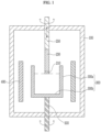
- FIG. 1 is a schematic cross-sectional view of the manufacturing apparatus used when growing the silicon carbide single crystal.
- the manufacturing apparatus of the silicon carbide single crystal may include a reaction chamber 100, a crucible 300 disposed inside of the reaction chamber 100, a seed crystal 210 extended to the inside of the crucible 300, a seed crystal support portion 230 connected to the seed crystal 210, a moving member 250, and a heating member 400 for heating the crucible 300.
- the reaction chamber 100 has a closed and sealed form to include an empty interior space, and the inside may be maintained by an atmosphere such as constant pressure.
- a vacuum pump and a gas tank for controlling atmosphere may be connected to the reaction chamber 100.
- the vacuum pump and the gas tank for controlling atmosphere are used to vacuum the inside of the reaction chamber 100, and then inert gas such as argon gas may be filled therein.
- the silicon carbide seed crystal 210 may be connected to the seed crystal support portion 230 and the moving member 250 to be disposed inside of the crucible 300, and in particular, to be disposed so that the seed crystal may be in contact with the fused solution provided inside of the crucible 300.
- This fused solution may include the above-described silicon-based fusion composition.
- a meniscus may be formed between the surface of the silicon carbide seed crystal 210 and the fused solution.
- the meniscus refers to a curved surface formed on the fused solution by surface tension occurring when the lower surface of the silicon carbide seed crystal 210 is brought into contact with the fused solution and then slightly lifted.
- the silicon carbide single crystal is grown by forming the meniscus, occurrence of the polycrystal is suppressed, thereby obtaining a higher quality single crystal.
- the silicon carbide seed crystal 210 is formed of a silicon carbide single crystal.
- the crystal structure of the silicon carbide seed crystal 210 is the same as the silicon carbide single crystal to be manufactured.
- a 4H polytype silicon carbide single crystal is manufactured, a 4H polytype silicon carbide seed crystal 210 may be used.
- a crystal growth surface may be the (0001) plane or (000-1) plane, or an inclined surface at an angle of 8° or less from the (0001) plane or (000-1) plane.
- the seed crystal support portion 230 connects the seed crystal 210 and the moving member 250. One end of the seed crystal support portion 230 may be connected to the moving member 250, and the other end may be connected to the seed crystal 210.
- the seed crystal support portion 230 is connected to the moving member 250 and may be moved in a vertical direction along the height direction of the crucible 300. Specifically, the seed crystal support portion 230 may be moved to the inside of the crucible 300 for the growth process of the silicon carbide single crystal, or moved to the outside of the crucible 300 after finishing the growth process of the silicon carbide single crystal. In addition, in the present specification, the exemplary embodiment in which the seed crystal support portion 230 is moved in a vertical direction is described, but not limited thereto, and the seed crystal support portion 230 may be moved or rotated in any direction, and a known means for this may be included.
- the seed crystal support portion 230 may be attached to and detached from the moving member 250.
- the seed crystal support portion 230 may be coupled to the moving member 250 so that the seed crystal is provided inside of the crucible 300 for obtaining the silicon carbide single crystal, and separated from the moving member 250 after the growth process of the single crystal is finished.
- the moving member 250 may be connected to a driving portion (not shown) to move or rotate the inside of the chamber 100.
- the moving member 250 may include a known means for vertical moving or rotating.
- the crucible 300 may be provided inside of the reaction chamber 100, in the form of a container having an opened upper side, and include an external circumferential surface 300a and a lower surface 300b, except an upper surface.
- the crucible 300 may be in any form for forming the silicon carbide single crystal without limitation on the above-described forms.
- the crucible 300 may be charged with and contain fusion raw materials such as silicon or silicon carbide powder.
- the crucible 300 may be made of a carbon-containing material such as graphite and silicon carbide, and the crucible 300 made of the material itself may be utilized as a source of a carbon raw material. Otherwise, without limitation thereto, a crucible made of ceramic may be used, and in this case, a material or source for providing carbon may be provided separately.
- the heating member 400 may heat the crucible 300 to fuse or heat the material contained in the crucible 300.
- the heating member 400 may use a resistance type heating means or induction heating type heating means. Specifically, heats may be formed in a resistive manner in which the heating member 400 itself generates heats, or in an induction heating manner in which the heating member 400 is formed by an induction coil and high-frequency current is allowed to flow in the induction coil, thereby heating the crucible 300.
- the method is not limited thereto, and any heating member may be used, of course.
- the manufacturing apparatus of silicon carbide may further include the rotating member 500.
- the rotating member 500 may be coupled to a lower side of the crucible 300 to rotate the crucible 300. Since a fused solution having a uniform composition may be provided by rotating the crucible 300, the silicon carbide single crystal having high quality may grow in the silicon carbide seed crystal 210.
- initial fusion raw materials including the above-described silicon-based fusion composition are added to the crucible 300.
- the initial fusion raw material may be in a powder form, but not limited thereto.
- the initial fusion raw material may not include carbon separately, but not limited thereto, and the initial fusion raw material may include carbon.
- the crucible 300 containing the initial raw material is heated using the heating member 400 under an inert atmosphere such as argon gas.
- an inert atmosphere such as argon gas.
- the initial fusion raw material in the crucible 300 is changed to the fused solution including carbon (C), silicon (Si) and metals (first metal, scandium, aluminum).
- the temperature of the fused solution in the crucible 300 is slowly lowered, and the carbon solubility in the fused solution is decreased. For this reason, when a silicon carbide supersaturation state is reached in the vicinity of the seed crystal 210, the silicon carbide single crystal grows on the seed crystal 210 using the supersaturation as driving force.
- silicon carbide single crystal grows, a condition to precipitate silicon carbide from the fused solution may be changed.
- silicon and carbon are added to adapt the composition of the fused solution over time, thereby maintaining the fused solution to have a composition within a certain range. Silicon and carbon to be added may be added continuously or discontinuously.
- the growth speed of the single crystal to be obtained may be high, thereby reducing time and cost required for the process.
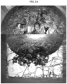
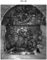
- FIGS. 2A , FIG. 2B , FIG. 2C , FIG. 2D and FIG. 2E is an image of the surface and the cross section of a solidified product precipitated by a slow cooling method, according to Comparative Example 1, Comparative Example 2, Example 1, Example 2 and Example 3.
- FIG. 2A is an image for Comparative Example 1 including Si 0.56 Cr 0.4 Al 0.04
- FIG. 2B is an image for Comparative Example 2 including Si 0.56 Cr 0.2 Sc 0.2 Al 0.04
- FIG. 2C is an image for Example 1 including Si 0.56 Cr 0.38 Sc 0.02 Al 0.04
- FIG. 2D is an image for Example 2 including Si 0.56 Cr 0.36 Sc 0.04 Al 0.04
- FIG. 2E is an image for Example 3 including Si 0.56 Cr 0.32 Sc 0.08 Al 0.04 .
- the inside of the crucible made of graphite is charged with the initial raw materials according to the chemical composition of Comparative Examples 1 and 2, and Examples 1 to 3, at about 30% by volume. Thereafter, the crucible is fused at 1900 degrees (°C) for 2 hours, cooled to 1600 degrees (°C) at a rate of 1 degree (°C) per minute, and then rapidly cooled, thereby obtaining a crucible having a solidified product formed therein. Thereafter, the crucible was cut, and carbon solubility characteristics and silicon carbide crystallization characteristics depending on each Example and Comparative Example were observed. The carbon solubility of the solidified product was observed using a C-S analyzer.
- Comparative Example 1 Si 0.56 Cr 0.4 Al 0.04
- a solidified product in a stable form may be obtained, but a silicon carbide precipitate having a hexagon shape was not found on the surface of the solidified product, and the erosion degree of the crucible was confirmed to be low.
- the erosion degree of the crucible represents that the carbon solubility in the fused solution is low, and specifically, the carbon solubility of Comparative Example 1 was measured as 4.3%.
- Example 1 Si 0.56 Cr 0.38 Sc 0.02 Al 0.04 ) shown in FIG. 2C had a not-high erosion degree of the crucible, as compared with Comparative Example 1, however, it was visually observed that the silicon carbide crystal was precipitated on the surface of the solidified product.. In addition, as a result of analyzing the carbon solubility of the solidified product, the carbon solubility of about 5.7% was shown, and thus, high carbon solubility as compared with Comparative Example 1 was confirmed.
- Example 2 Si 0.56 Cr 0.36 Sc 0.04 Al 0.04 ) shown in FIG. 2D that a corner portion of the crucible was eroded, and a very big sized silicon carbide single crystal of about 8 mm was precipitated on the surface of the solidified product.
- the carbon solubility of the solidified product for Example 2 was measured as about 7.9%.
- Example 3 Si 0.56 Cr 0.32 Sc 0.08 Al 0.04 ) shown in FIG. 2E that the erosion degree of the crucible inner wall was significant, as compared with Examples 1 and 2, thereby having excellent carbon solubility.
- the carbon solubility of the solidified product for Example 3 was measured as about 10.6%, and it was confirmed that a large amount of hexagonal silicon carbide single crystals was precipitated on the surface of the solidified product.
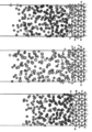
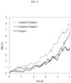
- FIGS. 3 and 4 Each of (a), (b) and (c) of FIG. 3 is an AIMD simulation image for reviewing the carbon solubility of Comparative Example 1 (Si 0.56 Cr 0.42 Al 0.04 ), Comparative Example 2 (Si 0.56 Sc 0.32 Al 0.04 ) and Example 1 (Si 0.46 Cr 0.43 Sc 0.08 Al 0.04 ), and FIG. 4 is a graph which analyzes the mean squared displacement (MSD) of the carbon atom for Comparative Example 1, Comparative Example 2 and Example 1 of (a), (b) and (c) of FIG. 3 .
- MSD mean squared displacement
- Example 1 was confirmed to have a high mean squared displacement value of the carbon atom, as compared with Comparative Examples 1 and 2. This means that the fused composition using chromium-scandium (Cr 43 at%-Sc 8at%) has a higher carbon solubility than the chemical composition using chromium (Cr 42 at%) or scandium (32 at%) alone, thereby capable of improving a crystal growth speed.
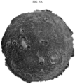
- FIG. 5A is an image of growth of the silicon carbide single crystal according to the Comparative Example (Si 0.56 Cr 0.4 Al 0.04 )
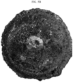
- FIG. 5B is an image of growth of the silicon carbide single crystal according to the Example (Si 0.56 Cr 0.36 Sc 0.04 Al 0.04 ).
- the silicon-based fusion composition according to an exemplary embodiment of the present invention may provide the silicon carbide single crystal having high quality, and also reduce time and cost required for the process by a rapid growth speed.
Landscapes
- Chemical & Material Sciences (AREA)
- Engineering & Computer Science (AREA)
- Crystallography & Structural Chemistry (AREA)
- Materials Engineering (AREA)
- Metallurgy (AREA)
- Organic Chemistry (AREA)
- Inorganic Chemistry (AREA)
- Crystals, And After-Treatments Of Crystals (AREA)
Claims (7)
- Siliciumschmelzzusammensetzung für ein Lösungswachstumsverfahren zum Bilden eines Siliciumcarbid-Einkristalls, umfassend:
Silicium, ein erstes Metall (M1), Scandium (Sc) und Aluminium (Al), wie durch die folgende Formel 1 dargestellt:
SiaM1bSccAld (Formel 1)
wobei a mehr als 0,5 und weniger als 0,7 beträgt, b mehr als 0,2 und weniger als 0,4 beträgt, c mehr als 0,01 und weniger als 0,1 beträgt und d mehr als 0,01 und weniger als 0,05 beträgt und das erste Metall (M1) eines oder mehrere ausgewählt aus der Gruppe bestehend aus Titan (Ti), Chrom (Cr), Vanadium (V), Yttrium (Y), Mangan (Mn), Eisen (Fe), Kobalt (Co), Bor (B), Cer (Ce), Lanthan (La) und Praseodym (Pr) ist. - Siliciumschmelzzusammensetzung nach Anspruch 1, bei der die Siliciumschmelzzusammensetzung eine Kohlenstofflöslichkeit von 5% oder mehr aufweist.
- Siliciumschmelzlösung, umfassend: die Siliciumschmelzzusammensetzung nach Anspruch 1 und Kohlenstoff, wobei das Scandium eine Kohlenstofflöslichkeit in der Siliciumschmelzlösung erhöht.
- Herstellungsverfahren für einen Siliciumcarbid-Einkristall, umfassend:Herstellen eines Siliciumcarbid-Impfkristalls;Herstellen einer Siliciumschmelzzusammensetzung, umfassend: Silicium (Si), ein erstes Metall (M1), Scandium (Sc) und Aluminium (Al), wie durch die folgende Formel 1 dargestellt:
SiaM1bSccAld (Formel 1)
wobei a mehr als 0,5 und weniger als 0,7 beträgt, b mehr als 0,2 und weniger als 0,4 beträgt, c mehr als 0,01 und weniger als 0,1 beträgt und d mehr als 0,01 und weniger als 0,05 beträgt; das erste Metall (M1) eines oder mehrere ausgewählt aus der Gruppe bestehend aus Titan (Ti), Chrom (Cr), Vanadium (V), Yttrium (Y), Mangan (Mn), Eisen (Fe), Kobalt (Co), Bor (B), Cer (Ce), Lanthan (La) und Praseodym (Pr) ist;Zugeben von Kohlenstoff (C) zu der Siliciumschmelzzusammensetzung, um eine Schmelzlösung zu bilden, undUnterkühlen der Schmelzlösung, um den Siliciumcarbid-Einkristall auf dem Impfkristall zu züchten. - Herstellungsverfahren für einen Siliciumcarbid-Einkristall nach Anspruch 4, bei dem die Siliciumschmelzzusammensetzung eine Kohlenstofflöslichkeit von 5% oder mehr aufweist.
- Herstellungsverfahren für einen Siliciumcarbid-Einkristall nach Anspruch 4, bei dem das Scandium eine Kohlenstofflöslichkeit in der Schmelzlösung erhöht.
- Herstellungsverfahren für einen Siliciumcarbid-Einkristall nach Anspruch 4, bei dem eine Wachstumsgeschwindigkeit des Siliciumcarbids 80 µm/h oder mehr beträgt.
Applications Claiming Priority (2)
| Application Number | Priority Date | Filing Date | Title |
|---|---|---|---|
| KR1020170082781A KR102142424B1 (ko) | 2017-06-29 | 2017-06-29 | 실리콘계 용융 조성물 및 이를 이용하는 실리콘카바이드 단결정의 제조 방법 |
| PCT/KR2018/006161 WO2019004611A1 (ko) | 2017-06-29 | 2018-05-30 | 실리콘계 용융 조성물 및 이를 이용하는 실리콘카바이드 단결정의 제조 방법 |
Publications (3)
| Publication Number | Publication Date |
|---|---|
| EP3575451A1 EP3575451A1 (de) | 2019-12-04 |
| EP3575451A4 EP3575451A4 (de) | 2020-01-22 |
| EP3575451B1 true EP3575451B1 (de) | 2024-08-28 |
Family
ID=64741991
Family Applications (1)
| Application Number | Title | Priority Date | Filing Date |
|---|---|---|---|
| EP18824134.3A Active EP3575451B1 (de) | 2017-06-29 | 2018-05-30 | Geschmolzene zusammensetzung auf siliciumbasis und verfahren zur herstellung von siliciumkarbideinkristallen damit |
Country Status (6)
| Country | Link |
|---|---|
| US (1) | US11203818B2 (de) |
| EP (1) | EP3575451B1 (de) |
| JP (1) | JP6821896B2 (de) |
| KR (1) | KR102142424B1 (de) |
| CN (1) | CN110382751B (de) |
| WO (1) | WO2019004611A1 (de) |
Families Citing this family (2)
| Publication number | Priority date | Publication date | Assignee | Title |
|---|---|---|---|---|
| JP7581810B2 (ja) * | 2020-12-04 | 2024-11-13 | 株式会社プロテリアル | 炭化ケイ素単結晶の製造方法 |
| CN115478324A (zh) * | 2022-08-31 | 2022-12-16 | 昆明理工大学 | 一种助溶剂法生长单晶或多晶SiC晶体的方法 |
Family Cites Families (19)
| Publication number | Priority date | Publication date | Assignee | Title |
|---|---|---|---|---|
| JP3876628B2 (ja) | 2001-02-07 | 2007-02-07 | 株式会社デンソー | 炭化珪素単結晶の製造方法および炭化珪素単結晶 |
| JP4453348B2 (ja) | 2003-11-25 | 2010-04-21 | トヨタ自動車株式会社 | 炭化珪素単結晶の製造方法 |
| JP4419937B2 (ja) | 2005-09-16 | 2010-02-24 | 住友金属工業株式会社 | 炭化珪素単結晶の製造方法 |
| JP4179331B2 (ja) | 2006-04-07 | 2008-11-12 | トヨタ自動車株式会社 | SiC単結晶の製造方法 |
| JP4586857B2 (ja) | 2008-02-06 | 2010-11-24 | トヨタ自動車株式会社 | p型SiC半導体単結晶の製造方法 |
| JP5244007B2 (ja) | 2009-03-26 | 2013-07-24 | 国立大学法人名古屋大学 | 3C−SiC単結晶の製造方法 |
| JP5218348B2 (ja) | 2009-09-03 | 2013-06-26 | 新日鐵住金株式会社 | 炭化珪素単結晶の製造方法 |
| WO2011040240A1 (ja) | 2009-09-29 | 2011-04-07 | 富士電機ホールディングス株式会社 | SiC単結晶およびその製造方法 |
| JP5273131B2 (ja) | 2010-11-26 | 2013-08-28 | 信越化学工業株式会社 | SiC単結晶の製造方法 |
| JP5273130B2 (ja) | 2010-11-26 | 2013-08-28 | 信越化学工業株式会社 | SiC単結晶の製造方法 |
| JP6128588B2 (ja) | 2013-02-28 | 2017-05-17 | 国立研究開発法人産業技術総合研究所 | SiC単結晶、その製造方法およびその表面清浄化方法 |
| WO2014189008A1 (ja) | 2013-05-20 | 2014-11-27 | 日立化成株式会社 | 炭化珪素単結晶及びその製造方法 |
| JP6062045B2 (ja) * | 2013-05-31 | 2017-01-18 | 新日鐵住金株式会社 | SiC単結晶の製造装置及び当該製造装置を用いるSiC単結晶の製造方法 |
| US20160273126A1 (en) | 2013-11-12 | 2016-09-22 | Nippon Steel & Sumitomo Metal Corporation | METHOD FOR PRODUCING SiC SINGLE CRYSTAL |
| JP6216060B2 (ja) * | 2015-01-29 | 2017-10-18 | 京セラ株式会社 | 結晶の製造方法 |
| JP2016169126A (ja) | 2015-03-13 | 2016-09-23 | 京セラ株式会社 | 結晶の製造方法 |
| JP2016185884A (ja) | 2015-03-27 | 2016-10-27 | 京セラ株式会社 | 結晶の製造方法 |
| JP6725096B2 (ja) * | 2015-10-26 | 2020-07-15 | エルジー・ケム・リミテッド | シリコン系溶融組成物およびこれを用いたSiC単結晶の製造方法 |
| WO2018062689A1 (ko) * | 2016-09-29 | 2018-04-05 | 주식회사 엘지화학 | 실리콘계 용융 조성물 및 이를 이용하는 실리콘카바이드 단결정의 제조 방법 |
-
2017
- 2017-06-29 KR KR1020170082781A patent/KR102142424B1/ko active Active
-
2018
- 2018-05-30 JP JP2019543926A patent/JP6821896B2/ja active Active
- 2018-05-30 EP EP18824134.3A patent/EP3575451B1/de active Active
- 2018-05-30 CN CN201880012928.8A patent/CN110382751B/zh active Active
- 2018-05-30 US US16/494,523 patent/US11203818B2/en active Active
- 2018-05-30 WO PCT/KR2018/006161 patent/WO2019004611A1/ko not_active Ceased
Also Published As
| Publication number | Publication date |
|---|---|
| CN110382751B (zh) | 2021-05-11 |
| EP3575451A4 (de) | 2020-01-22 |
| KR102142424B1 (ko) | 2020-08-07 |
| EP3575451A1 (de) | 2019-12-04 |
| US20200010973A1 (en) | 2020-01-09 |
| WO2019004611A1 (ko) | 2019-01-03 |
| JP2020508277A (ja) | 2020-03-19 |
| JP6821896B2 (ja) | 2021-01-27 |
| CN110382751A (zh) | 2019-10-25 |
| KR20190002207A (ko) | 2019-01-08 |
| US11203818B2 (en) | 2021-12-21 |
Similar Documents
| Publication | Publication Date | Title |
|---|---|---|
| TWI554659B (zh) | SiC單晶的製造方法 | |
| JP5273130B2 (ja) | SiC単結晶の製造方法 | |
| CN101796227B (zh) | 碳化硅单晶的生长方法 | |
| JP5218348B2 (ja) | 炭化珪素単結晶の製造方法 | |
| EP3406769B1 (de) | Siliciumbasierte schmelzzusammensetzung und verfahren zur herstellung eines siliciumcarbid-einkristalls mittels dieser | |
| JP5273131B2 (ja) | SiC単結晶の製造方法 | |
| US11203818B2 (en) | Silicon based fusion composition and manufacturing method of silicon carbide single crystal using the same | |
| KR102136269B1 (ko) | 실리콘카바이드 단결정의 제조 장치 | |
| EP4130347A1 (de) | Verfahren zur herstellung eines sic-einkristalls | |
| JP7072146B2 (ja) | 鉄ガリウム合金の単結晶育成方法 | |
| KR102091629B1 (ko) | 실리콘계 용융 조성물 및 이를 이용하는 실리콘카바이드 단결정의 제조 방법 | |
| KR102158624B1 (ko) | 실리콘계 용융 조성물 및 이를 이용하는 실리콘카바이드 단결정의 제조 방법 | |
| EP3636806B1 (de) | Siliciumbasierte schmelzzusammensetzung und verfahren zur herstellung eines siliciumcarbideinkristalls unter verwendung davon | |
| KR102673789B1 (ko) | 실리콘카바이드 단결정의 제조 방법 | |
| WO2019053856A9 (ja) | ヒ化ガリウム系化合物半導体結晶およびウエハ群 | |
| KR20180091344A (ko) | 실리콘카바이드 단결정의 제조 방법 | |
| KR20210004735A (ko) | 실리콘카바이드 단결정의 제조 방법 | |
| JP2005350324A (ja) | SiC単結晶の製造方法 | |
| KR102601625B1 (ko) | 실리콘카바이드 단결정의 제조 방법 | |
| WO2019088740A2 (ko) | 실리콘계 용융 조성물 및 이를 이용하는 실리콘카바이드 단결정의 제조 방법 |
Legal Events
| Date | Code | Title | Description |
|---|---|---|---|
| STAA | Information on the status of an ep patent application or granted ep patent |
Free format text: STATUS: THE INTERNATIONAL PUBLICATION HAS BEEN MADE |
|
| PUAI | Public reference made under article 153(3) epc to a published international application that has entered the european phase |
Free format text: ORIGINAL CODE: 0009012 |
|
| STAA | Information on the status of an ep patent application or granted ep patent |
Free format text: STATUS: REQUEST FOR EXAMINATION WAS MADE |
|
| 17P | Request for examination filed |
Effective date: 20190830 |
|
| AK | Designated contracting states |
Kind code of ref document: A1 Designated state(s): AL AT BE BG CH CY CZ DE DK EE ES FI FR GB GR HR HU IE IS IT LI LT LU LV MC MK MT NL NO PL PT RO RS SE SI SK SM TR |
|
| AX | Request for extension of the european patent |
Extension state: BA ME |
|
| A4 | Supplementary search report drawn up and despatched |
Effective date: 20191220 |
|
| RIC1 | Information provided on ipc code assigned before grant |
Ipc: C30B 29/06 20060101ALI20191216BHEP Ipc: C30B 29/36 20060101AFI20191216BHEP Ipc: C30B 9/04 20060101ALI20191216BHEP Ipc: C30B 9/06 20060101ALI20191216BHEP |
|
| STAA | Information on the status of an ep patent application or granted ep patent |
Free format text: STATUS: EXAMINATION IS IN PROGRESS |
|
| DAV | Request for validation of the european patent (deleted) | ||
| DAX | Request for extension of the european patent (deleted) | ||
| 17Q | First examination report despatched |
Effective date: 20200917 |
|
| GRAP | Despatch of communication of intention to grant a patent |
Free format text: ORIGINAL CODE: EPIDOSNIGR1 |
|
| STAA | Information on the status of an ep patent application or granted ep patent |
Free format text: STATUS: GRANT OF PATENT IS INTENDED |
|
| INTG | Intention to grant announced |
Effective date: 20240529 |
|
| GRAS | Grant fee paid |
Free format text: ORIGINAL CODE: EPIDOSNIGR3 |
|
| GRAA | (expected) grant |
Free format text: ORIGINAL CODE: 0009210 |
|
| STAA | Information on the status of an ep patent application or granted ep patent |
Free format text: STATUS: THE PATENT HAS BEEN GRANTED |
|
| AK | Designated contracting states |
Kind code of ref document: B1 Designated state(s): AL AT BE BG CH CY CZ DE DK EE ES FI FR GB GR HR HU IE IS IT LI LT LU LV MC MK MT NL NO PL PT RO RS SE SI SK SM TR |
|
| REG | Reference to a national code |
Ref country code: GB Ref legal event code: FG4D |
|
| REG | Reference to a national code |
Ref country code: CH Ref legal event code: EP |
|
| REG | Reference to a national code |
Ref country code: DE Ref legal event code: R096 Ref document number: 602018073717 Country of ref document: DE |
|
| REG | Reference to a national code |
Ref country code: IE Ref legal event code: FG4D |
|
| REG | Reference to a national code |
Ref country code: LT Ref legal event code: MG9D |
|
| PG25 | Lapsed in a contracting state [announced via postgrant information from national office to epo] |
Ref country code: NO Free format text: LAPSE BECAUSE OF FAILURE TO SUBMIT A TRANSLATION OF THE DESCRIPTION OR TO PAY THE FEE WITHIN THE PRESCRIBED TIME-LIMIT Effective date: 20241128 |
|
| REG | Reference to a national code |
Ref country code: AT Ref legal event code: MK05 Ref document number: 1718042 Country of ref document: AT Kind code of ref document: T Effective date: 20240828 |
|
| PG25 | Lapsed in a contracting state [announced via postgrant information from national office to epo] |
Ref country code: PT Free format text: LAPSE BECAUSE OF FAILURE TO SUBMIT A TRANSLATION OF THE DESCRIPTION OR TO PAY THE FEE WITHIN THE PRESCRIBED TIME-LIMIT Effective date: 20241230 Ref country code: NL Free format text: LAPSE BECAUSE OF FAILURE TO SUBMIT A TRANSLATION OF THE DESCRIPTION OR TO PAY THE FEE WITHIN THE PRESCRIBED TIME-LIMIT Effective date: 20240828 Ref country code: GR Free format text: LAPSE BECAUSE OF FAILURE TO SUBMIT A TRANSLATION OF THE DESCRIPTION OR TO PAY THE FEE WITHIN THE PRESCRIBED TIME-LIMIT Effective date: 20241129 Ref country code: PL Free format text: LAPSE BECAUSE OF FAILURE TO SUBMIT A TRANSLATION OF THE DESCRIPTION OR TO PAY THE FEE WITHIN THE PRESCRIBED TIME-LIMIT Effective date: 20240828 Ref country code: FI Free format text: LAPSE BECAUSE OF FAILURE TO SUBMIT A TRANSLATION OF THE DESCRIPTION OR TO PAY THE FEE WITHIN THE PRESCRIBED TIME-LIMIT Effective date: 20240828 |
|
| PG25 | Lapsed in a contracting state [announced via postgrant information from national office to epo] |
Ref country code: BG Free format text: LAPSE BECAUSE OF FAILURE TO SUBMIT A TRANSLATION OF THE DESCRIPTION OR TO PAY THE FEE WITHIN THE PRESCRIBED TIME-LIMIT Effective date: 20240828 |
|
| PG25 | Lapsed in a contracting state [announced via postgrant information from national office to epo] |
Ref country code: LV Free format text: LAPSE BECAUSE OF FAILURE TO SUBMIT A TRANSLATION OF THE DESCRIPTION OR TO PAY THE FEE WITHIN THE PRESCRIBED TIME-LIMIT Effective date: 20240828 |
|
| REG | Reference to a national code |
Ref country code: NL Ref legal event code: MP Effective date: 20240828 |
|
| PG25 | Lapsed in a contracting state [announced via postgrant information from national office to epo] |
Ref country code: IS Free format text: LAPSE BECAUSE OF FAILURE TO SUBMIT A TRANSLATION OF THE DESCRIPTION OR TO PAY THE FEE WITHIN THE PRESCRIBED TIME-LIMIT Effective date: 20241228 Ref country code: AT Free format text: LAPSE BECAUSE OF FAILURE TO SUBMIT A TRANSLATION OF THE DESCRIPTION OR TO PAY THE FEE WITHIN THE PRESCRIBED TIME-LIMIT Effective date: 20240828 |
|
| PG25 | Lapsed in a contracting state [announced via postgrant information from national office to epo] |
Ref country code: HR Free format text: LAPSE BECAUSE OF FAILURE TO SUBMIT A TRANSLATION OF THE DESCRIPTION OR TO PAY THE FEE WITHIN THE PRESCRIBED TIME-LIMIT Effective date: 20240828 |
|
| PG25 | Lapsed in a contracting state [announced via postgrant information from national office to epo] |
Ref country code: ES Free format text: LAPSE BECAUSE OF FAILURE TO SUBMIT A TRANSLATION OF THE DESCRIPTION OR TO PAY THE FEE WITHIN THE PRESCRIBED TIME-LIMIT Effective date: 20240828 Ref country code: RS Free format text: LAPSE BECAUSE OF FAILURE TO SUBMIT A TRANSLATION OF THE DESCRIPTION OR TO PAY THE FEE WITHIN THE PRESCRIBED TIME-LIMIT Effective date: 20241128 |
|
| PG25 | Lapsed in a contracting state [announced via postgrant information from national office to epo] |
Ref country code: RS Free format text: LAPSE BECAUSE OF FAILURE TO SUBMIT A TRANSLATION OF THE DESCRIPTION OR TO PAY THE FEE WITHIN THE PRESCRIBED TIME-LIMIT Effective date: 20241128 Ref country code: PT Free format text: LAPSE BECAUSE OF FAILURE TO SUBMIT A TRANSLATION OF THE DESCRIPTION OR TO PAY THE FEE WITHIN THE PRESCRIBED TIME-LIMIT Effective date: 20241230 Ref country code: PL Free format text: LAPSE BECAUSE OF FAILURE TO SUBMIT A TRANSLATION OF THE DESCRIPTION OR TO PAY THE FEE WITHIN THE PRESCRIBED TIME-LIMIT Effective date: 20240828 Ref country code: NO Free format text: LAPSE BECAUSE OF FAILURE TO SUBMIT A TRANSLATION OF THE DESCRIPTION OR TO PAY THE FEE WITHIN THE PRESCRIBED TIME-LIMIT Effective date: 20241128 Ref country code: NL Free format text: LAPSE BECAUSE OF FAILURE TO SUBMIT A TRANSLATION OF THE DESCRIPTION OR TO PAY THE FEE WITHIN THE PRESCRIBED TIME-LIMIT Effective date: 20240828 Ref country code: LV Free format text: LAPSE BECAUSE OF FAILURE TO SUBMIT A TRANSLATION OF THE DESCRIPTION OR TO PAY THE FEE WITHIN THE PRESCRIBED TIME-LIMIT Effective date: 20240828 Ref country code: IS Free format text: LAPSE BECAUSE OF FAILURE TO SUBMIT A TRANSLATION OF THE DESCRIPTION OR TO PAY THE FEE WITHIN THE PRESCRIBED TIME-LIMIT Effective date: 20241228 Ref country code: HR Free format text: LAPSE BECAUSE OF FAILURE TO SUBMIT A TRANSLATION OF THE DESCRIPTION OR TO PAY THE FEE WITHIN THE PRESCRIBED TIME-LIMIT Effective date: 20240828 Ref country code: GR Free format text: LAPSE BECAUSE OF FAILURE TO SUBMIT A TRANSLATION OF THE DESCRIPTION OR TO PAY THE FEE WITHIN THE PRESCRIBED TIME-LIMIT Effective date: 20241129 Ref country code: FI Free format text: LAPSE BECAUSE OF FAILURE TO SUBMIT A TRANSLATION OF THE DESCRIPTION OR TO PAY THE FEE WITHIN THE PRESCRIBED TIME-LIMIT Effective date: 20240828 Ref country code: ES Free format text: LAPSE BECAUSE OF FAILURE TO SUBMIT A TRANSLATION OF THE DESCRIPTION OR TO PAY THE FEE WITHIN THE PRESCRIBED TIME-LIMIT Effective date: 20240828 Ref country code: BG Free format text: LAPSE BECAUSE OF FAILURE TO SUBMIT A TRANSLATION OF THE DESCRIPTION OR TO PAY THE FEE WITHIN THE PRESCRIBED TIME-LIMIT Effective date: 20240828 Ref country code: AT Free format text: LAPSE BECAUSE OF FAILURE TO SUBMIT A TRANSLATION OF THE DESCRIPTION OR TO PAY THE FEE WITHIN THE PRESCRIBED TIME-LIMIT Effective date: 20240828 |
|
| PG25 | Lapsed in a contracting state [announced via postgrant information from national office to epo] |
Ref country code: SM Free format text: LAPSE BECAUSE OF FAILURE TO SUBMIT A TRANSLATION OF THE DESCRIPTION OR TO PAY THE FEE WITHIN THE PRESCRIBED TIME-LIMIT Effective date: 20240828 Ref country code: RO Free format text: LAPSE BECAUSE OF FAILURE TO SUBMIT A TRANSLATION OF THE DESCRIPTION OR TO PAY THE FEE WITHIN THE PRESCRIBED TIME-LIMIT Effective date: 20240828 Ref country code: DK Free format text: LAPSE BECAUSE OF FAILURE TO SUBMIT A TRANSLATION OF THE DESCRIPTION OR TO PAY THE FEE WITHIN THE PRESCRIBED TIME-LIMIT Effective date: 20240828 |
|
| PG25 | Lapsed in a contracting state [announced via postgrant information from national office to epo] |
Ref country code: EE Free format text: LAPSE BECAUSE OF FAILURE TO SUBMIT A TRANSLATION OF THE DESCRIPTION OR TO PAY THE FEE WITHIN THE PRESCRIBED TIME-LIMIT Effective date: 20240828 |
|
| PG25 | Lapsed in a contracting state [announced via postgrant information from national office to epo] |
Ref country code: CZ Free format text: LAPSE BECAUSE OF FAILURE TO SUBMIT A TRANSLATION OF THE DESCRIPTION OR TO PAY THE FEE WITHIN THE PRESCRIBED TIME-LIMIT Effective date: 20240828 |
|
| PG25 | Lapsed in a contracting state [announced via postgrant information from national office to epo] |
Ref country code: IT Free format text: LAPSE BECAUSE OF FAILURE TO SUBMIT A TRANSLATION OF THE DESCRIPTION OR TO PAY THE FEE WITHIN THE PRESCRIBED TIME-LIMIT Effective date: 20240828 Ref country code: SK Free format text: LAPSE BECAUSE OF FAILURE TO SUBMIT A TRANSLATION OF THE DESCRIPTION OR TO PAY THE FEE WITHIN THE PRESCRIBED TIME-LIMIT Effective date: 20240828 |
|
| REG | Reference to a national code |
Ref country code: DE Ref legal event code: R097 Ref document number: 602018073717 Country of ref document: DE |
|
| PLBE | No opposition filed within time limit |
Free format text: ORIGINAL CODE: 0009261 |
|
| STAA | Information on the status of an ep patent application or granted ep patent |
Free format text: STATUS: NO OPPOSITION FILED WITHIN TIME LIMIT |
|
| PGFP | Annual fee paid to national office [announced via postgrant information from national office to epo] |
Ref country code: DE Payment date: 20250422 Year of fee payment: 8 |
|
| PGFP | Annual fee paid to national office [announced via postgrant information from national office to epo] |
Ref country code: FR Payment date: 20250422 Year of fee payment: 8 |
|
| 26N | No opposition filed |
Effective date: 20250530 |
|
| PG25 | Lapsed in a contracting state [announced via postgrant information from national office to epo] |
Ref country code: SE Free format text: LAPSE BECAUSE OF FAILURE TO SUBMIT A TRANSLATION OF THE DESCRIPTION OR TO PAY THE FEE WITHIN THE PRESCRIBED TIME-LIMIT Effective date: 20240828 |
|
| REG | Reference to a national code |
Ref country code: CH Ref legal event code: H13 Free format text: ST27 STATUS EVENT CODE: U-0-0-H10-H13 (AS PROVIDED BY THE NATIONAL OFFICE) Effective date: 20251223 |
|
| PG25 | Lapsed in a contracting state [announced via postgrant information from national office to epo] |
Ref country code: LU Free format text: LAPSE BECAUSE OF NON-PAYMENT OF DUE FEES Effective date: 20250530 |
|
| PG25 | Lapsed in a contracting state [announced via postgrant information from national office to epo] |
Ref country code: CH Free format text: LAPSE BECAUSE OF NON-PAYMENT OF DUE FEES Effective date: 20250531 |
|
| REG | Reference to a national code |
Ref country code: BE Ref legal event code: MM Effective date: 20250531 |
|
| PG25 | Lapsed in a contracting state [announced via postgrant information from national office to epo] |
Ref country code: MC Free format text: LAPSE BECAUSE OF FAILURE TO SUBMIT A TRANSLATION OF THE DESCRIPTION OR TO PAY THE FEE WITHIN THE PRESCRIBED TIME-LIMIT Effective date: 20240828 |
|
| PGFP | Annual fee paid to national office [announced via postgrant information from national office to epo] |
Ref country code: GB Payment date: 20260324 Year of fee payment: 9 |
|
| PG25 | Lapsed in a contracting state [announced via postgrant information from national office to epo] |
Ref country code: IE Free format text: LAPSE BECAUSE OF NON-PAYMENT OF DUE FEES Effective date: 20250530 |
|
| PG25 | Lapsed in a contracting state [announced via postgrant information from national office to epo] |
Ref country code: BE Free format text: LAPSE BECAUSE OF NON-PAYMENT OF DUE FEES Effective date: 20250531 |