EP3545548B1 - Integrated circuit nanoparticle thermal routing structure in interconnect region - Google Patents
Integrated circuit nanoparticle thermal routing structure in interconnect region Download PDFInfo
- Publication number
- EP3545548B1 EP3545548B1 EP17874052.8A EP17874052A EP3545548B1 EP 3545548 B1 EP3545548 B1 EP 3545548B1 EP 17874052 A EP17874052 A EP 17874052A EP 3545548 B1 EP3545548 B1 EP 3545548B1
- Authority
- EP
- European Patent Office
- Prior art keywords
- routing structure
- integrated circuit
- nanoparticles
- forming
- interconnect region
- Prior art date
- Legal status (The legal status is an assumption and is not a legal conclusion. Google has not performed a legal analysis and makes no representation as to the accuracy of the status listed.)
- Active
Links
Images


Classifications
-
- H—ELECTRICITY
- H01—ELECTRIC ELEMENTS
- H01L—SEMICONDUCTOR DEVICES NOT COVERED BY CLASS H10
- H01L23/00—Details of semiconductor or other solid state devices
- H01L23/34—Arrangements for cooling, heating, ventilating or temperature compensation ; Temperature sensing arrangements
- H01L23/36—Selection of materials, or shaping, to facilitate cooling or heating, e.g. heatsinks
- H01L23/367—Cooling facilitated by shape of device
- H01L23/3677—Wire-like or pin-like cooling fins or heat sinks
-
- H—ELECTRICITY
- H01—ELECTRIC ELEMENTS
- H01L—SEMICONDUCTOR DEVICES NOT COVERED BY CLASS H10
- H01L23/00—Details of semiconductor or other solid state devices
- H01L23/34—Arrangements for cooling, heating, ventilating or temperature compensation ; Temperature sensing arrangements
- H01L23/36—Selection of materials, or shaping, to facilitate cooling or heating, e.g. heatsinks
- H01L23/367—Cooling facilitated by shape of device
-
- H—ELECTRICITY
- H01—ELECTRIC ELEMENTS
- H01L—SEMICONDUCTOR DEVICES NOT COVERED BY CLASS H10
- H01L21/00—Processes or apparatus adapted for the manufacture or treatment of semiconductor or solid state devices or of parts thereof
- H01L21/02—Manufacture or treatment of semiconductor devices or of parts thereof
- H01L21/04—Manufacture or treatment of semiconductor devices or of parts thereof the devices having potential barriers, e.g. a PN junction, depletion layer or carrier concentration layer
- H01L21/48—Manufacture or treatment of parts, e.g. containers, prior to assembly of the devices, using processes not provided for in a single one of the groups H01L21/18 - H01L21/326 or H10D48/04 - H10D48/07
- H01L21/4814—Conductive parts
- H01L21/4871—Bases, plates or heatsinks
- H01L21/4882—Assembly of heatsink parts
-
- H—ELECTRICITY
- H01—ELECTRIC ELEMENTS
- H01L—SEMICONDUCTOR DEVICES NOT COVERED BY CLASS H10
- H01L21/00—Processes or apparatus adapted for the manufacture or treatment of semiconductor or solid state devices or of parts thereof
- H01L21/70—Manufacture or treatment of devices consisting of a plurality of solid state components formed in or on a common substrate or of parts thereof; Manufacture of integrated circuit devices or of parts thereof
- H01L21/71—Manufacture of specific parts of devices defined in group H01L21/70
- H01L21/768—Applying interconnections to be used for carrying current between separate components within a device comprising conductors and dielectrics
- H01L21/76801—Applying interconnections to be used for carrying current between separate components within a device comprising conductors and dielectrics characterised by the formation and the after-treatment of the dielectrics, e.g. smoothing
-
- H—ELECTRICITY
- H01—ELECTRIC ELEMENTS
- H01L—SEMICONDUCTOR DEVICES NOT COVERED BY CLASS H10
- H01L21/00—Processes or apparatus adapted for the manufacture or treatment of semiconductor or solid state devices or of parts thereof
- H01L21/70—Manufacture or treatment of devices consisting of a plurality of solid state components formed in or on a common substrate or of parts thereof; Manufacture of integrated circuit devices or of parts thereof
- H01L21/71—Manufacture of specific parts of devices defined in group H01L21/70
- H01L21/768—Applying interconnections to be used for carrying current between separate components within a device comprising conductors and dielectrics
- H01L21/76838—Applying interconnections to be used for carrying current between separate components within a device comprising conductors and dielectrics characterised by the formation and the after-treatment of the conductors
- H01L21/76877—Filling of holes, grooves or trenches, e.g. vias, with conductive material
-
- H—ELECTRICITY
- H01—ELECTRIC ELEMENTS
- H01L—SEMICONDUCTOR DEVICES NOT COVERED BY CLASS H10
- H01L23/00—Details of semiconductor or other solid state devices
- H01L23/34—Arrangements for cooling, heating, ventilating or temperature compensation ; Temperature sensing arrangements
- H01L23/36—Selection of materials, or shaping, to facilitate cooling or heating, e.g. heatsinks
- H01L23/373—Cooling facilitated by selection of materials for the device or materials for thermal expansion adaptation, e.g. carbon
- H01L23/3731—Ceramic materials or glass
-
- H—ELECTRICITY
- H01—ELECTRIC ELEMENTS
- H01L—SEMICONDUCTOR DEVICES NOT COVERED BY CLASS H10
- H01L23/00—Details of semiconductor or other solid state devices
- H01L23/34—Arrangements for cooling, heating, ventilating or temperature compensation ; Temperature sensing arrangements
- H01L23/36—Selection of materials, or shaping, to facilitate cooling or heating, e.g. heatsinks
- H01L23/373—Cooling facilitated by selection of materials for the device or materials for thermal expansion adaptation, e.g. carbon
- H01L23/3733—Cooling facilitated by selection of materials for the device or materials for thermal expansion adaptation, e.g. carbon having a heterogeneous or anisotropic structure, e.g. powder or fibres in a matrix, wire mesh, porous structures
-
- H—ELECTRICITY
- H01—ELECTRIC ELEMENTS
- H01L—SEMICONDUCTOR DEVICES NOT COVERED BY CLASS H10
- H01L23/00—Details of semiconductor or other solid state devices
- H01L23/34—Arrangements for cooling, heating, ventilating or temperature compensation ; Temperature sensing arrangements
- H01L23/36—Selection of materials, or shaping, to facilitate cooling or heating, e.g. heatsinks
- H01L23/373—Cooling facilitated by selection of materials for the device or materials for thermal expansion adaptation, e.g. carbon
- H01L23/3736—Metallic materials
-
- H—ELECTRICITY
- H01—ELECTRIC ELEMENTS
- H01L—SEMICONDUCTOR DEVICES NOT COVERED BY CLASS H10
- H01L23/00—Details of semiconductor or other solid state devices
- H01L23/48—Arrangements for conducting electric current to or from the solid state body in operation, e.g. leads, terminal arrangements ; Selection of materials therefor
- H01L23/481—Internal lead connections, e.g. via connections, feedthrough structures
-
- H—ELECTRICITY
- H01—ELECTRIC ELEMENTS
- H01L—SEMICONDUCTOR DEVICES NOT COVERED BY CLASS H10
- H01L23/00—Details of semiconductor or other solid state devices
- H01L23/52—Arrangements for conducting electric current within the device in operation from one component to another, i.e. interconnections, e.g. wires, lead frames
- H01L23/522—Arrangements for conducting electric current within the device in operation from one component to another, i.e. interconnections, e.g. wires, lead frames including external interconnections consisting of a multilayer structure of conductive and insulating layers inseparably formed on the semiconductor body
- H01L23/5226—Via connections in a multilevel interconnection structure
-
- H—ELECTRICITY
- H01—ELECTRIC ELEMENTS
- H01L—SEMICONDUCTOR DEVICES NOT COVERED BY CLASS H10
- H01L24/00—Arrangements for connecting or disconnecting semiconductor or solid-state bodies; Methods or apparatus related thereto
- H01L24/01—Means for bonding being attached to, or being formed on, the surface to be connected, e.g. chip-to-package, die-attach, "first-level" interconnects; Manufacturing methods related thereto
- H01L24/02—Bonding areas ; Manufacturing methods related thereto
- H01L24/04—Structure, shape, material or disposition of the bonding areas prior to the connecting process
- H01L24/05—Structure, shape, material or disposition of the bonding areas prior to the connecting process of an individual bonding area
-
- H—ELECTRICITY
- H01—ELECTRIC ELEMENTS
- H01L—SEMICONDUCTOR DEVICES NOT COVERED BY CLASS H10
- H01L24/00—Arrangements for connecting or disconnecting semiconductor or solid-state bodies; Methods or apparatus related thereto
- H01L24/01—Means for bonding being attached to, or being formed on, the surface to be connected, e.g. chip-to-package, die-attach, "first-level" interconnects; Manufacturing methods related thereto
- H01L24/02—Bonding areas ; Manufacturing methods related thereto
- H01L24/04—Structure, shape, material or disposition of the bonding areas prior to the connecting process
- H01L24/06—Structure, shape, material or disposition of the bonding areas prior to the connecting process of a plurality of bonding areas
-
- H—ELECTRICITY
- H01—ELECTRIC ELEMENTS
- H01L—SEMICONDUCTOR DEVICES NOT COVERED BY CLASS H10
- H01L21/00—Processes or apparatus adapted for the manufacture or treatment of semiconductor or solid state devices or of parts thereof
- H01L21/70—Manufacture or treatment of devices consisting of a plurality of solid state components formed in or on a common substrate or of parts thereof; Manufacture of integrated circuit devices or of parts thereof
- H01L21/71—Manufacture of specific parts of devices defined in group H01L21/70
- H01L21/768—Applying interconnections to be used for carrying current between separate components within a device comprising conductors and dielectrics
- H01L21/76801—Applying interconnections to be used for carrying current between separate components within a device comprising conductors and dielectrics characterised by the formation and the after-treatment of the dielectrics, e.g. smoothing
- H01L21/76829—Applying interconnections to be used for carrying current between separate components within a device comprising conductors and dielectrics characterised by the formation and the after-treatment of the dielectrics, e.g. smoothing characterised by the formation of thin functional dielectric layers, e.g. dielectric etch-stop, barrier, capping or liner layers
-
- H—ELECTRICITY
- H01—ELECTRIC ELEMENTS
- H01L—SEMICONDUCTOR DEVICES NOT COVERED BY CLASS H10
- H01L2224/00—Indexing scheme for arrangements for connecting or disconnecting semiconductor or solid-state bodies and methods related thereto as covered by H01L24/00
- H01L2224/01—Means for bonding being attached to, or being formed on, the surface to be connected, e.g. chip-to-package, die-attach, "first-level" interconnects; Manufacturing methods related thereto
- H01L2224/10—Bump connectors; Manufacturing methods related thereto
- H01L2224/12—Structure, shape, material or disposition of the bump connectors prior to the connecting process
- H01L2224/13—Structure, shape, material or disposition of the bump connectors prior to the connecting process of an individual bump connector
- H01L2224/13001—Core members of the bump connector
- H01L2224/1302—Disposition
- H01L2224/13025—Disposition the bump connector being disposed on a via connection of the semiconductor or solid-state body
-
- H—ELECTRICITY
- H01—ELECTRIC ELEMENTS
- H01L—SEMICONDUCTOR DEVICES NOT COVERED BY CLASS H10
- H01L2224/00—Indexing scheme for arrangements for connecting or disconnecting semiconductor or solid-state bodies and methods related thereto as covered by H01L24/00
- H01L2224/01—Means for bonding being attached to, or being formed on, the surface to be connected, e.g. chip-to-package, die-attach, "first-level" interconnects; Manufacturing methods related thereto
- H01L2224/10—Bump connectors; Manufacturing methods related thereto
- H01L2224/12—Structure, shape, material or disposition of the bump connectors prior to the connecting process
- H01L2224/14—Structure, shape, material or disposition of the bump connectors prior to the connecting process of a plurality of bump connectors
- H01L2224/1451—Function
- H01L2224/14515—Bump connectors having different functions
- H01L2224/14519—Bump connectors having different functions including bump connectors providing primarily thermal dissipation
-
- H—ELECTRICITY
- H01—ELECTRIC ELEMENTS
- H01L—SEMICONDUCTOR DEVICES NOT COVERED BY CLASS H10
- H01L23/00—Details of semiconductor or other solid state devices
- H01L23/52—Arrangements for conducting electric current within the device in operation from one component to another, i.e. interconnections, e.g. wires, lead frames
- H01L23/522—Arrangements for conducting electric current within the device in operation from one component to another, i.e. interconnections, e.g. wires, lead frames including external interconnections consisting of a multilayer structure of conductive and insulating layers inseparably formed on the semiconductor body
- H01L23/532—Arrangements for conducting electric current within the device in operation from one component to another, i.e. interconnections, e.g. wires, lead frames including external interconnections consisting of a multilayer structure of conductive and insulating layers inseparably formed on the semiconductor body characterised by the materials
- H01L23/5329—Insulating materials
- H01L23/53295—Stacked insulating layers
Definitions
- This relates to integrated circuits, and more particularly to thermal management in integrated circuits.
- Integrated circuits frequently generate undesired heat in some active components. It is sometimes desired to remove the heat through a heat sink or other passive structure. It is sometimes desired to divert the heat from thermally sensitive components in the integrated circuit. Managing excess heat in integrated circuits has become increasingly problematic.
- US 2016/093551 discloses thermal management structures in microelectronic devices.
- an integrated circuit according to claim 1 and a method of forming an integrated circuit according to claim 10. Additional aspects are specified in the dependent claims.
- an integrated circuit has a substrate and an interconnect region disposed on the substrate.
- the interconnect region has a plurality of interconnect levels.
- the integrated circuit includes a thermal routing structure in the interconnect region.
- the thermal routing structure extends over a portion, but not all, of the integrated circuit in the interconnect region.
- the thermal routing structure includes a cohered nanoparticle film in which adjacent nanoparticles cohere to each other.
- the thermal routing structure has a thermal conductivity higher than dielectric material touching the thermal routing structure.
- the cohered nanoparticle film is formed by a method which includes an additive process.
- instant top surface of an integrated circuit refers to the top surface of the integrated circuit, which exists at the particular step being described.
- the instant top surface may change from step to step in the formation of the integrated circuit.
- lateral refers to a direction parallel to a plane of an instant top surface of the integrated circuit
- vertical refers to a direction perpendicular to the plane of the instant top surface of the integrated circuit
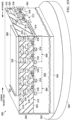
- FIG. 1A and FIG. 1B are cross sections of an example integrated circuit containing a thermal routing structure according to an embodiment.
- the integrated circuit 100 includes a substrate 102 including a semiconductor material 104 such as silicon, silicon germanium or silicon carbide. Alternatively, the semiconductor material 104 may be a type III-V semiconductor such as gallium nitride or gallium arsenide. Other semiconductor materials are within the scope of this example.
- the integrated circuit 100 further includes an interconnect region 106 disposed above the substrate 102. Heat-generating components 108 of the integrated circuit 100, depicted in FIG.
- the integrated circuit 100 may also include thermally sensitive components 112, depicted in FIG. 1A as MOS transistors.
- the components 108 and 112 may be laterally separated by field oxide 114 at the boundary 110 between the substrate 102 and the interconnect region 106.
- the field oxide 114 may have a shallow trench isolation (STI) structure as depicted in FIG. 1A , or may have a localized oxidation of silicon (LOCOS) structure.
- STI shallow trench isolation
- LOC localized oxidation of silicon
- the interconnect region 106 may include contacts 116, interconnects 118 and vias 120 disposed in a dielectric layer stack 122.
- the contacts 116 make electrical connections to the heat-generating components 108 and the thermally sensitive components 112.
- the interconnects 118 are disposed in a plurality of interconnect levels.
- the interconnects 118 in a first interconnect level make electrical connections to the contacts 116.
- the vias 120 are disposed between successive interconnect levels and make electrical connections to the interconnects.
- a top surface 124 of the interconnect region 106 is located at a surface of the interconnect region 106 opposite to the boundary 110 between the substrate 102 and the interconnect region 106.
- the interconnects 118 may include aluminum interconnects, damascene copper interconnects, and/or plated copper interconnects.
- An aluminum interconnect may include an aluminum layer with a few percent silicon, titanium, and/or copper, possibly on an adhesion layer including titanium, and possibly with an anti-reflection layer of titanium nitride on the aluminum layer.
- a damascene copper interconnect may include copper on a barrier layer of tantalum and/or tantalum nitride, disposed in a trench in the dielectric layer stack 122.
- a plated copper interconnect may include an adhesion layer at a bottom of the interconnect, and may have a barrier layer disposed on the sides of the interconnect.
- Bond pad structures 126 may be disposed over the top surface 124 of the interconnect region 106, and may be electrically coupled to the interconnects 118.
- a protective overcoat 128 may be disposed over the top surface 124 of the interconnect region 106.
- the protective overcoat 128 may include one or more layers of dielectric material, such as silicon dioxide, silicon nitride, silicon oxide nitride, and/or polyimide.
- a thermal routing structure 130 is disposed in the interconnect region 106, extending over a portion, but not all, of the integrated circuit 100 in the interconnect region 106.
- the thermal routing structure 130 has a higher thermal conductivity than dielectric material in the interconnect region 106 that touches the thermal routing structure 130.
- Thermal conductivity is a property of a material, and may be expressed in units of watts / meter °C.
- the thermal routing structure 130 includes a cohered nanoparticle film 132 including primarily nanoparticles 133, shown in more detail in FIG. 1B . Adjacent nanoparticles 133 cohere to each other.
- the thermal routing structure 130 is substantially free of an organic binder material such as adhesive or polymer.
- the thermal routing structure 130 may extend from an area over the heat-generating components 108 to a heat removal region 134 of the integrated circuit 100, as shown in FIG. 1A .
- the thermal routing structure 130 may be located outside an area over the thermally sensitive components 112, as shown in FIG. 1A , thus configured to advantageously divert heat from the heat-generating components 108 away from the thermally sensitive components 112 during operation of the integrated circuit 100.
- thermal routing structure 130 may be electrically non-conductive, and examples of the nanoparticles 133 may include nanoparticles of aluminum oxide, diamond, hexagonal boron nitride, cubic boron nitride, and/or aluminum nitride.
- the thermal routing structure 130 may touch the contacts 116, the interconnects 118, and/or the vias 120 without risking undesired electrical shunts, enabling more complete coverage of the area over the heat-generating components 108 and in the heat removal region 134, to advantageously collect more heat from the heat-generating components 108, and more efficiently deliver the heat to the heat removal region 134.
- the thermal routing structure 130 may be electrically conductive.
- examples of the nanoparticles 133 may include nanoparticles of metal, graphene, graphene embedded in metal, graphite, graphitic carbon, and/or carbon nanotubes. Electrically conductive versions of the thermal routing structure 130 may be separated from the contacts 116, the interconnects 118, and the vias 120.
- the nanoparticles 133 may include nanoparticles that include metal, and the thermal routing structure 130 may include a layer of graphitic material on the cohered nanoparticle film 132.
- examples of the nanoparticles 133 may include nanoparticles of copper, nickel, palladium, platinum, iridium, rhodium, cerium, osmium, molybdenum, and/or gold.
- the thermal routing structure 130 is electrically conductive, and hence may be separated from the contacts 116, the interconnects 118, and the vias 120.
- An optional planarization layer 136 may be disposed laterally adjacent to the thermal routing structure 130 to provide a substantially level surface for subsequent layers of the dielectric layer stack 122 and subsequent interconnect levels.
- the planarization layer 136 may have a thickness comparable to a thickness of the thermal routing structure 130.
- the planarization layer 136 may have a thermal conductivity comparable to a thermal conductivity of the dielectric layer stack 122, which is significantly less than the thermal conductivity of the thermal routing structure 130.
- the planarization layer 136 may include dielectric materials such as silicon dioxide and may have a granular structure.
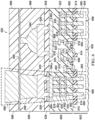
- FIG. 2A through FIG. 2F depict an example method of forming an integrated circuit with a thermal routing structure according to an embodiment.
- the integrated circuit 200 is formed on a substrate 202 which includes a semiconductor material 204.
- the substrate 202 may be a semiconductor wafer.
- the semiconductor material 204 may be a type IV semiconductor such as silicon, silicon germanium or silicon carbide.
- the semiconductor material 204 may be a type III-V semiconductor such as gallium nitride or gallium arsenide. Other semiconductor materials are within the scope of this example.
- Components are formed in the semiconductor material 204, such as heat-generating components 208 and thermally sensitive components 212.
- the components may include MOS transistors, bipolar junction transistors, JFETs, resistors, SCRs, diodes and/or other components.
- Field oxide 214 may be formed in the substrate 202 to laterally separate the components.
- the field oxide 214 may be formed by an STI process or alternatively by a LOCOS process.
- An interconnect region 206 is formed over the substrate 202.
- FIG. 2A shows the interconnect region 206 at a stage partway through completion.
- the interconnect region 206 may be formed as a series of dielectric layers to form a dielectric layer stack 222, with interconnect elements formed in each of the dielectric layers.
- a pre-metal dielectric (PMD) layer of the dielectric layer stack 222 may be formed directly over the substrate 202, and contacts 216 may be subsequently formed through the PMD layer to make electrical connections to the components, including the heat-generating components 208 and the thermally sensitive components 212.
- a first intra-metal dielectric (IMD) layer is formed as part of the dielectric layer stack 222.
- Interconnects 218 in a first interconnect level in the first IMD layer are formed over the PMD layer and the contacts 216.
- the interconnects 218 in the first interconnect level make electrical connections to the contacts 216.
- a portion of a first inter-level dielectric (ILD) layer may be formed over the first IMD layer and first interconnect level, as part of the dielectric layer stack 222.
- ILD inter-level dielectric
- Forming the thermal routing structure of this example begins with forming a nanoparticle ink film 238 of a nanoparticle ink 240 by an additive process 242 over an instant top surface of the interconnect region 206.
- an additive process disposes the nanoparticles in a desired area and does not dispose the nanoparticles outside of the desired area, so a final desired shape of the nanoparticles is produced without needing to remove a portion of the dispensed nanoparticles.
- Additive processes may enable forming films in desired areas without photolithographic processes and subsequent etch processes, thus advantageously reducing fabrication cost and complexity.
- the nanoparticle ink 240 includes the nanoparticles and a carrier fluid.
- the nanoparticle ink 240 may be an ink, a slurry, or a sol gel.
- the nanoparticles may include materials described for the nanoparticles 133 in reference to FIG. 1A and FIG. 1B .
- a composition of the nanoparticle ink 240 may be selected to provide a desired adhesion to the integrated circuit 200.
- the nanoparticle ink 240 is dispensed onto the integrated circuit 200 in an area for the subsequently-formed thermal routing structure, and is not dispensed over the entire instant top surface of the interconnect region 206.
- the additive process 242 may include a discrete droplet process, sometimes referred to as an inkjet process, using a discrete droplet dispensing apparatus 243.
- the discrete droplet dispensing apparatus 243 may be configured so that the integrated circuit 200 and the discrete droplet dispensing apparatus 243 may be moved laterally with respect to each other to provide a desired dispensing pattern for the nanoparticle ink film 238.
- the discrete droplet dispensing apparatus 243 may have a plurality of dispensing ports which may be independently activated in parallel to provide a desired throughput for the additive process 242.
- the additive process 242 may include a continuous extrusion process, a direct laser transfer process, an electrostatic deposition process, or an electrochemical deposition process.
- vias may be formed in the first ILD, making electrical connections to the interconnects 218 in the first interconnect level. Additional IMD layers with interconnects in sequential interconnect levels, and additional ILD layers with vias, may be formed in the interconnect region 206, before formation of the thermal routing structure.
- the nanoparticle ink film 238 of FIG. 2A is heated by a bake process 244 to remove at least a portion of a volatile material from the nanoparticle ink film 238 to form a nanoparticle film 246 which includes primarily nanoparticles.
- the first bake process 244 may be a radiant heat process, such as using an incandescent light source 245 as indicated schematically in FIG. 2B , or infrared light emitting diodes (IR LEDs).
- the bake process 244 may be a hot plate process which heats the nanoparticle ink film 238 through the substrate 202.
- the bake process 244 may be performed in a partial vacuum, or in an ambient with a continuous flow of gas at low pressure, to enhance removal of the volatile material.
- Cohesion may also occur by a process that includes a chemical mechanism involving reaction of atoms between the adjacent nanoparticles.
- the cohesion inducing process 248 may include heating by a scanning laser apparatus 249 as depicted schematically in FIG. 2C .
- the scanning laser apparatus 249 may be configured to provide heat to substantially only the nanoparticle film 246 and not provide heat to portions of the integrated circuit 200 laterally adjacent to the nanoparticle film 246, advantageously reducing a total heat load on the components 208 and 212.
- the cohesion inducing process 248 may include a flash heating process, which applies radiant energy for 1 microsecond to 10 microseconds. In another variation, the cohesion inducing process 248 may include a spike heating process, which applies radiant energy for 100 milliseconds to 5 seconds.
- the bake process 244 described in reference to FIG. 2B may be combined with the cohesion inducing process 248, wherein thermal power applied to the nanoparticle film 246 of FIG. 2B is ramped to first remove the volatile material, followed by inducing cohesion of the nanoparticles. Other methods of inducing cohesion between the nanoparticles are within the scope of this example.
- the cohered nanoparticle film 250 may provide the thermal routing structure 230.
- the steps described in reference to FIG. 2A through FIG. 2C may be repeated to form a second cohered nanoparticle film, that in combination with the cohered nanoparticle film 250, provides the thermal routing structure 230 with a desired thickness.
- Some parameters of the process steps, such as bake time and temperature, may be adjusted to accommodate more than one cohered nanoparticle film in the thermal routing structure 230.
- a planarization layer similar to the planarization layer 136 described in reference to FIG. 1A , may optionally be formed that is laterally adjacent to the thermal routing structure 230, to provide a substantially level surface which facilitates formation of subsequent layers of the interconnect region 206.
- the planarization layer may be formed by any of various methods; this example discloses forming the planarization layer using an additive process. Formation of the planarization layer begins with forming a slurry layer 251 by an additive process 252 on the instant top surface of the interconnect region 206 laterally adjacent to the thermal routing structure 230.
- the slurry layer 251 may include dielectric grains dispersed in an aqueous fluid or possibly an organic binder precursor fluid.
- the additive process 252 may use a continuous dispensing apparatus 253 as depicted schematically in FIG. 2D , or may use another additive apparatus such as a discrete droplet dispenser.
- the slurry layer 251 may be dispensed onto substantially all of the instant top surface of the interconnect region 206 that is not covered by the thermal routing structure 230.
- the slurry layer 251 is heated by a slurry bake process 254 to remove at least a portion of a volatile material from the slurry layer 251.
- the slurry bake process 254 may be a radiant heat process using an incandescent source 255, as indicated in FIG. 2E , or may be a hot plate bake process, a forced air bake process, or a combination thereof.
- the slurry layer 251 of FIG. 2E is cured to form the planarization layer 236.
- the slurry layer 251 may be cured by a heat process 256 using a heat lamp 258, as indicated in FIG. 2F , or by exposure to ultraviolet radiation to polymerize an organic precursor in the slurry layer 251.
- Formation of the interconnect region 206 continues with formation of dielectric layers of the dielectric layer stack 222 and formation of vias.
- the vias may be formed through the thermal routing structure 230, and through the planarization layer 236 if present, with appropriate adjustments to etch process for forming via holes.
- FIG. 3A through FIG. 3C depict another example method of forming an integrated circuit with a thermal routing structure according to an embodiment.
- the integrated circuit 300 is formed on a substrate 302 which includes a semiconductor material 304.
- Components are formed in the semiconductor material 304, proximate to a top surface 310 of the substrate 302.
- the components of this example may include a first set of components 308 and a second set of components 360, wherein the first set of components 308 is spatially separated from the second set of components 360, and wherein the first set of components 308 and the second set of components 360 benefit from sharing a same thermal environment.
- the first set of components 308 and the second set of components 360 may be matching components of an analog circuit.
- Matching components are designed to have substantially equal performance parameters, such as drive current and threshold. Because these performance parameters are affected by temperature, reducing a temperature difference between matching components may advantageously reduce differences in the performance parameters.
- the components 308 and 360 may include MOS transistors, bipolar junction transistors, JFETs, resistors, SCRs, diodes and/or other components.
- Field oxide 314 may be formed in the substrate 302 to laterally separate the components. The field oxide 314 may be formed by an STI process or alternatively by a LOCOS process.
- FIG. 3A shows the interconnect region 306 at a stage partway through completion.
- the interconnect region 306 may be formed as a series of dielectric layers, such as a PMD layer, and alternating IMD layers and ILD layers, to form a dielectric layer stack 322, with interconnect elements such as contacts 316, interconnects 318, and vias 320 formed in the dielectric layers.
- Forming the thermal routing structure of this example may begin with optionally forming a dielectric isolation layer 362 over an instant top surface of the interconnect region 306.
- the dielectric isolation layer 362 may electrically isolate the interconnects 318 from the subsequently formed thermal routing structure.
- the dielectric isolation layer 362 may include silicon dioxide-based dielectric material.
- the dielectric isolation layer 362 may be formed by a plasma enhanced chemical vapor deposition (PECVD) process using tetraethyl orthosilicate (TEOS), or spin coating the integrated circuit 300 with hydrogen silsesquioxane (HSQ) or methyl silsesquioxane (MSQ) followed by baking and annealing.
- PECVD plasma enhanced chemical vapor deposition
- TEOS tetraethyl orthosilicate
- HSQ hydrogen silsesquioxane
- MSQ methyl silsesquioxane
- the dielectric isolation layer 362 may be configured as a blanket layer or may be patterned.
- a patterned manifestation of the dielectric isolation layer 362 may be formed of electrically non-conductive nanoparticles having a high thermal conductivity, which may advantageously increase an overall thermal conductivity of the thermal routing structure.
- forming the dielectric isolation layer may be omitted.
- a nanoparticle ink film 338 of a nanoparticle ink 340 is formed on an instant top surface of the interconnect region 306.
- the nanoparticle ink film 338 is formed by an additive process 342.
- the nanoparticle ink 340 may include electrically conductive nanoparticles and a carrier fluid.
- the nanoparticle ink 340 is dispensed onto the integrated circuit 300 in an area for the subsequently-formed thermal routing structure, and is not dispensed over the entire instant top surface of the interconnect region 306.
- the nanoparticle ink 340 may be omitted outside of areas for subsequently formed vias, so as to leave via openings 364 in the nanoparticle ink film 338, to avoid the electrically conductive nanoparticles touching the subsequently formed vias.
- the additive process 342 may use a continuous micro-extrusion dispensing apparatus 343, as indicted schematically in FIG. 3A .
- the continuous micro-extrusion dispensing apparatus 343 may be configured so that the integrated circuit 300 and the continuous micro-extrusion dispensing apparatus 343 may be moved laterally with respect to each other to provide a desired dispensing pattern for the nanoparticle ink film 338.
- the nanoparticle ink film 338 of FIG. 3A is heated by a bake process 344 to remove at least a portion of a volatile material from the nanoparticle ink film 338 to form a nanoparticle film 346 which includes primarily nanoparticles.
- the bake process 344 may be a hot plate process using a hot plate 345 disposed under the substrate 302, as depicted in FIG. 3B .
- the bake process 344 may be a radiant heat process, as described in reference to FIG. 2B .
- the bake process 344 may be performed in a partial vacuum, or in an ambient with a continuous flow of gas at low pressure, to enhance removal of the volatile material.
- the nanoparticle film 346 of FIG. 3B is heated by a cohesion inducing process 348 so that adjacent nanoparticles cohere to each other, to form a cohered nanoparticle film 350.
- the cohesion inducing process 348 may include a flash heating process using a flash lamp 366, as depicted schematically in FIG. 3C . Other methods of inducing cohesion between the nanoparticles are within the scope of this example.
- the cohered nanoparticle film 350 may provide substantially all of the thermal routing structure 330. Alternatively, additional cohered nanoparticle films may be formed to combine with the cohered nanoparticle film 350 to provide the thermal routing structure 330.
- FIG. 4A and FIG. 4B are cross sections of another example integrated circuit containing a thermal routing structure according to an embodiment.
- the integrated circuit 400 includes a substrate 402 including a semiconductor material 404.
- the integrated circuit 400 further includes an interconnect region 406 disposed above the substrate 402.
- a first set of components 408 and a second set of components 460 are disposed in the substrate 402 and the interconnect region 406, proximate to a boundary 410 between the substrate 402 and the interconnect region 406.
- the first set of components 408 and the second set of components 460 may be matching components whose performance benefits from having similar thermal environments.
- the integrated circuit 400 may further include thermally sensitive components 412 whose performance improves as a temperature decreases.
- the components 408, 460 and 412 are depicted in FIG. 4A as MOS transistors, but other manifestations (such as bipolar junction transistors, JFETs, resistors, and SCRs) are within the scope of this example.
- the components 408, 460 and 412 may be laterally separated by field oxide 414 at the boundary 410 between the substrate 402 and the interconnect region 406.
- the interconnect region 406 may include contacts 416, interconnects 418 and vias 420 disposed in a dielectric layer stack 422.
- a top surface 424 of the interconnect region 406 is located at a surface of the interconnect region 406 opposite to the boundary 410 between the substrate 402 and the interconnect region 406.
- Bond pad structures 426 may be disposed over the top surface 424 of the interconnect region 406, and are electrically coupled to the interconnects 418.
- a protective overcoat 428 may be disposed over the top surface 424 of the interconnect region 406. The bond pad structures 426 may extend through the protective overcoat 428.
- a thermal routing structure 430 is disposed in the interconnect region 406, extending over a portion, but not all, of the integrated circuit 400 in the interconnect region 406.
- the thermal routing structure 430 includes a cohered nanoparticle film 432 including nanoparticles 433 which include metal, and a layer of graphitic material 468 disposed on the cohered nanoparticle film 432, shown in detail in FIG. 4B .
- the nanoparticles 433 may include copper, nickel, palladium, platinum, iridium, rhodium, cerium, osmium, molybdenum, and/or gold.
- the layer of graphitic material 468 may include graphite, graphitic carbon, graphene, carbon nanotubes or the like.
- a dielectric isolation layer 470 may optionally be disposed under the thermal routing structure 430.
- the dielectric isolation layer 470 may electrically isolate the layer of cohered nanoparticle film 432 from underlying interconnects 418.
- the thermal routing structure 430 may extend over the first set of components 408 and the second set of components 460, and may extend away the thermally sensitive components 412, as shown in FIG. 4A .
- the thermal routing structure 430 may provide a more closely matched thermal environment for the first set of components 408 and the second set of components 460 and thereby improve their performance, while advantageously diverting heat from the first set of components 408 and the second set of components 460 away from the thermally sensitive components 412.
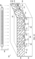
- FIG. 5A through FIG. 5D depict another example method of forming an integrated circuit with a thermal routing structure according to an embodiment.
- the integrated circuit 500 is formed on a substrate 502 which includes a semiconductor material 504.
- Components (such as heat-generating components 508, thermally sensitive components 512 and matching components 560) are formed in the semiconductor material 504 proximate to a top surface 510 of the substrate 502.
- the top surface 510 of the substrate 502 is also a boundary between the substrate 502 and the interconnect region 506.
- Field oxide 514 may be formed in the substrate 502 to laterally separate the components 508, 512 and 560.
- An interconnect region 506 is formed over the substrate 502.
- the interconnect region 506 may be formed to have a dielectric layer stack 522, with interconnect elements such as contacts 516, interconnects 518, and vias 520 formed in the dielectric layer stack 522.
- a dielectric isolation layer may optionally be formed in an area for the thermal routing structure.
- the dielectric isolation layer may be formed by any of various methods, such as described in reference to the dielectric isolation layer 362 of FIG. 3A .
- a nanoparticle ink film 538 containing nanoparticles which include metal is formed by an additive process 572 over an instant top surface of the interconnect region 506, on the dielectric isolation layer, if present.
- the nanoparticles may include the metals described in reference to FIG. 4A and FIG. 4B , or other metal suitable as a catalyst for subsequent growth of graphitic material.
- the nanoparticle ink film 538 is formed in an area for the subsequently-formed thermal routing structure, and is not formed over an entire instant top surface of the interconnect region 506.
- the additive process 572 may include a direct laser transfer process which uses a pulsed laser 573 to transfer small pieces of nanoparticle ink 574 of a source layer 576 containing the nanoparticles to the integrated circuit 500, as depicted in FIG. 5A .
- the source layer 576 is attached to a backing layer 578.
- the combined source layer 576 and backing layer 578 are sometimes referred to as a ribbon.
- the pulsed laser 573, the source layer 576 and backing layer 578, and the integrated circuit 500 may be moved relative to each other to form the nanoparticle ink film 538 in a desired area. Other methods of forming the nanoparticle ink film 538 are within the scope of this example.
- the nanoparticle ink film 538 of FIG. 5A may be heated by a bake process 544 to remove at least a portion of a volatile material from the nanoparticle ink film 538 to form a nanoparticle film 546 which includes primarily nanoparticles.
- the bake process 544 may be a radiant heat process using IR LEDs 545 as depicted schematically in FIG. 5B . Using the IR LEDs 545 may enable application of the radiant heat to substantially only an area containing the nanoparticle ink film 538 while not applying the radiant heat to areas of the integrated circuit 500 outside of the nanoparticle ink film 538, advantageously reducing a heat load on the components 508, 512, and 568.
- the bake process 544 may include a radiant heat process using an incandescent source, or may include a hot plate process.
- the nanoparticle film 546 of FIG. 5B is heated by a cohesion inducing process 548 so that adjacent nanoparticles cohere to each other, to form a cohered nanoparticle film 532.
- the cohesion inducing process 548 may include a spike heating process using an incandescent lamp 566, as depicted schematically in FIG. 5C .
- the spike heating process heats the nanoparticle film 546 for a time duration, such as for 1 millisecond to 10 milliseconds, to advantageously limit heating of the components 508, 512 and 568.
- Other methods of inducing cohesion between the nanoparticles are within the scope of this example.
- a layer of graphitic material 568 is selectively formed on the cohered nanoparticle film 532 by a graphitic material PECVD process.
- the substrate 502 is disposed on a wafer chuck 580 and is heated by the wafer chuck 580, such as to a temperature of 200 °C to 400 °C.
- a carbon-containing reagent gas denoted in FIG. 5D as "CARBON REAGENT GAS” is flowed over the integrated circuit 500 and radio frequency (RF) power, denoted in FIG. 5D as "RF POWER” is applied to the carbon-containing reagent gas to generate carbon radicals above the integrated circuit 500.
- RF radio frequency
- the carbon-containing reagent gas may include methane, straight chain alkanes such as ethane, propane and/or butane, alcohols such as ethanol, and/or cyclic hydrocarbons such as cyclobutane or benzene. Additional gases, such as hydrogen, argon and/or oxygen, may be flowed over the the integrated circuit 500.
- the nanoparticles in the cohered nanoparticle film 532 catalyze the carbon radicals to react to form the graphitic material 568, so that a first layer of the layer of graphitic material 568 is formed selectively on the cohered nanoparticle film 532.
- Subsequent layers of the graphitic material 568 are formed selectively on the previously formed layers of graphitic material 568, so that the layer of graphitic material 568 is formed selectively on the cohered nanoparticle film 532, and the graphitic material 568 is not formed on the integrated circuit 500 outside of the cohered nanoparticle film 532.
- the combined cohered nanoparticle film 532 and the layer of graphitic material 568 provide the thermal routing structure 530.
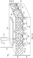
- FIG. 6 is a cross section of an example integrated circuit which includes a combined thermal routing structure according to an embodiment.
- the integrated circuit 600 includes a substrate 602 including a semiconductor material 604.
- the integrated circuit 600 further includes an interconnect region 606 disposed above the substrate 602.
- Heat-generating components 608 are disposed in the substrate 602 and the interconnect region 606, proximate to a boundary 610 between the substrate 602 and the interconnect region 606.
- the components 608 may be MOS transistors, bipolar junction transistors, JFETs, resistors, and/or SCRs.
- the components 608 may be laterally separated by field oxide 614 at the boundary 610 between the substrate 602 and the interconnect region 606.
- the interconnect region 606 may include contacts 616, interconnects 618 and vias 620 disposed in a dielectric layer stack 622. Some of the interconnects 618 are disposed in a top interconnect level 682 which is located proximate to a top surface 624 of the interconnect region 606. The top surface 624 of the interconnect region 606 is located opposite from the boundary 610 between the substrate 602 and the interconnect region 606. Bond pad structures 626 are disposed over the top surface 624 of the interconnect region 606, and are electrically coupled to the interconnects 618 in the top interconnect level 682. A protective overcoat 628 is disposed over the top surface 624 of the interconnect region 606.
- the integrated circuit 600 is assembled using wire bonds 684 on some of the bond pad structures 626.
- the integrated circuit 600 is packaged by encapsulation in an encapsulation material 686.
- the encapsulation material 686 such as an epoxy, is disposed over the protective overcoat 628 and the bond pad structures 626.
- the integrated circuit 600 of this example includes the combined thermal routing structure 688, which extends from inside the substrate 602 through the interconnect region 606, and through the organic polymer encapsulation material 686.
- the combined thermal routing structure 688 includes a thermal routing structure 630 disposed in the interconnect region 606 according to any of the examples herein.
- the combined thermal routing structure 688 may conduct heat generated by the components 608 to a heat removal apparatus, such as a heat sink, located outside of a package containing the integrated circuit 600, which may advantageously reduce an operating temperature of the components 608.
- the combined thermal routing structure 688 may include deep trench thermal routing structures 690 disposed in the substrate 602 and extending to the boundary 610 between the substrate 602 and the interconnect region 606.
- the deep trench thermal routing structures 690 may surround a portion of the components 608 and may be connected to each other at locations out of the plane of FIG. 6 .
- the deep trench thermal routing structures 690 may have structures and may be formed, such as described in Patent Application No. US 15/361,397 .
- the combined thermal routing structure 688 may include high thermal conductivity vias 692 disposed in the interconnect region 606.
- the high thermal conductivity vias 692 may surround a portion of the components 608 and may be connected to each other at locations out of the plane of FIG. 6 .
- the high thermal conductivity vias 692 may have structures and may be formed, such as described in Patent Application No. US 15/361,399 .
- the combined thermal routing structure 688 may include a top level thermal conductivity structure 694 disposed above the top interconnect level 682.
- the top level thermal conductivity structure 694 may have a structure and may be formed, such as described in Patent Application No. US 15/361,390 .
- the combined thermal routing structure 688 may include high thermal conductivity through-package conduits 696 disposed through the encapsulation material 686 to the integrated circuit 600.
- the high thermal conductivity through-package conduits 696 may have structures and may be formed, such as described in Patent Application No. US 15/361,403 .
- the integrated circuit 600 may further include graphitic material vias 698 which are electrically coupled to the components 608.
- the graphitic material vias 698 may conduct heat generated by the components 608 away from the substrate, possibly to the combined thermal routing structure 688, which may advantageously reduce an operating temperature of the components 608.
- the graphitic material vias 698 may have structures and may be formed, such as described in Patent Application No. US 15/361,401 .
Landscapes
- Engineering & Computer Science (AREA)
- Computer Hardware Design (AREA)
- Power Engineering (AREA)
- Microelectronics & Electronic Packaging (AREA)
- General Physics & Mathematics (AREA)
- Physics & Mathematics (AREA)
- Condensed Matter Physics & Semiconductors (AREA)
- Chemical & Material Sciences (AREA)
- Materials Engineering (AREA)
- Manufacturing & Machinery (AREA)
- Ceramic Engineering (AREA)
- Internal Circuitry In Semiconductor Integrated Circuit Devices (AREA)
- Cooling Or The Like Of Semiconductors Or Solid State Devices (AREA)
Applications Claiming Priority (2)
| Application Number | Priority Date | Filing Date | Title |
|---|---|---|---|
| US15/361,394 US10811334B2 (en) | 2016-11-26 | 2016-11-26 | Integrated circuit nanoparticle thermal routing structure in interconnect region |
| PCT/US2017/063136 WO2018098364A1 (en) | 2016-11-26 | 2017-11-22 | Integrated circuit nanoparticle thermal routing structure in interconnect region |
Publications (3)
| Publication Number | Publication Date |
|---|---|
| EP3545548A1 EP3545548A1 (en) | 2019-10-02 |
| EP3545548A4 EP3545548A4 (en) | 2019-12-25 |
| EP3545548B1 true EP3545548B1 (en) | 2025-06-11 |
Family
ID=62192788
Family Applications (1)
| Application Number | Title | Priority Date | Filing Date |
|---|---|---|---|
| EP17874052.8A Active EP3545548B1 (en) | 2016-11-26 | 2017-11-22 | Integrated circuit nanoparticle thermal routing structure in interconnect region |
Country Status (6)
| Country | Link |
|---|---|
| US (1) | US10811334B2 (enExample) |
| EP (1) | EP3545548B1 (enExample) |
| JP (1) | JP7045018B2 (enExample) |
| KR (1) | KR102473615B1 (enExample) |
| CN (1) | CN109937477B (enExample) |
| WO (1) | WO2018098364A1 (enExample) |
Families Citing this family (5)
| Publication number | Priority date | Publication date | Assignee | Title |
|---|---|---|---|---|
| JP7240149B2 (ja) | 2018-08-29 | 2023-03-15 | キオクシア株式会社 | 半導体装置 |
| US20200075508A1 (en) * | 2018-08-29 | 2020-03-05 | Toshiba Memory Corporation | Semiconductor device |
| US11049980B2 (en) | 2018-10-30 | 2021-06-29 | Texas Instruments Incorporated | Integrated MIM diode |
| US11239415B2 (en) * | 2019-04-18 | 2022-02-01 | Nanya Technology Corporation | Memory device and fabrication method thereof |
| US11658092B2 (en) * | 2020-11-13 | 2023-05-23 | Taiwan Semiconductor Manufacturing Company, Ltd. | Thermal interconnect structure for thermal management of electrical interconnect structure |
Family Cites Families (157)
| Publication number | Priority date | Publication date | Assignee | Title |
|---|---|---|---|---|
| US5224030A (en) | 1990-03-30 | 1993-06-29 | The United States Of America As Represented By The Administrator Of The National Aeronautics And Space Administration | Semiconductor cooling apparatus |
| US5481136A (en) | 1992-10-28 | 1996-01-02 | Sumitomo Electric Industries, Ltd. | Semiconductor element-mounting composite heat-sink base |
| US5683939A (en) | 1993-04-02 | 1997-11-04 | Harris Corporation | Diamond insulator devices and method of fabrication |
| US7067406B2 (en) | 1997-03-31 | 2006-06-27 | Intel Corporation | Thermal conducting trench in a semiconductor structure and method for forming the same |
| US6222254B1 (en) | 1997-03-31 | 2001-04-24 | Intel Corporation | Thermal conducting trench in a semiconductor structure and method for forming the same |
| US7368013B2 (en) | 1997-04-04 | 2008-05-06 | Chien-Min Sung | Superabrasive particle synthesis with controlled placement of crystalline seeds |
| US6046503A (en) | 1997-09-26 | 2000-04-04 | Siemens Aktiengesellschaft | Metalization system having an enhanced thermal conductivity |
| US5955781A (en) | 1998-01-13 | 1999-09-21 | International Business Machines Corporation | Embedded thermal conductors for semiconductor chips |
| JPH11238734A (ja) | 1998-02-20 | 1999-08-31 | Nec Corp | 半導体集積回路 |
| JP3347057B2 (ja) * | 1998-05-22 | 2002-11-20 | 株式会社東芝 | 半導体装置 |
| US6265771B1 (en) | 1999-01-27 | 2001-07-24 | International Business Machines Corporation | Dual chip with heat sink |
| US6288426B1 (en) | 2000-02-28 | 2001-09-11 | International Business Machines Corp. | Thermal conductivity enhanced semiconductor structures and fabrication processes |
| GB0022329D0 (en) | 2000-09-12 | 2000-10-25 | Mitel Semiconductor Ltd | Semiconductor device |
| US6512292B1 (en) | 2000-09-12 | 2003-01-28 | International Business Machines Corporation | Semiconductor chip structures with embedded thermal conductors and a thermal sink disposed over opposing substrate surfaces |
| JP4833398B2 (ja) | 2000-09-18 | 2011-12-07 | ポリマテック株式会社 | 熱伝導性成形体の製造方法 |
| JP2002097371A (ja) | 2000-09-20 | 2002-04-02 | Polymatech Co Ltd | 熱伝導性高分子組成物及び熱伝導性成形体 |
| US7161239B2 (en) | 2000-12-22 | 2007-01-09 | Broadcom Corporation | Ball grid array package enhanced with a thermal and electrical connector |
| JP4663153B2 (ja) | 2001-05-22 | 2011-03-30 | ポリマテック株式会社 | 熱伝導性複合材料組成物 |
| JP4714371B2 (ja) | 2001-06-06 | 2011-06-29 | ポリマテック株式会社 | 熱伝導性成形体及びその製造方法 |
| JP3791601B2 (ja) | 2002-02-08 | 2006-06-28 | 日本電気株式会社 | ナノグラファイト構造体の作製方法 |
| US6525419B1 (en) | 2002-02-14 | 2003-02-25 | Intel Corporation | Thermally coupling electrically decoupling cooling device for integrated circuits |
| US7071603B2 (en) | 2002-02-20 | 2006-07-04 | Cdream Corporation | Patterned seed layer suitable for electron-emitting device, and associated fabrication method |
| JP4416376B2 (ja) | 2002-05-13 | 2010-02-17 | 富士通株式会社 | 半導体装置及びその製造方法 |
| US6771502B2 (en) | 2002-06-28 | 2004-08-03 | Advanced Energy Technology Inc. | Heat sink made from longer and shorter graphite sheets |
| JP2004051852A (ja) | 2002-07-22 | 2004-02-19 | Polymatech Co Ltd | 熱伝導性高分子成形体及びその製造方法 |
| US7332211B1 (en) | 2002-11-07 | 2008-02-19 | Massachusetts Institute Of Technology | Layered materials including nanoparticles |
| JP2004175926A (ja) | 2002-11-27 | 2004-06-24 | Polymatech Co Ltd | 熱伝導性エポキシ樹脂成形体及びその製造方法 |
| DE10336747A1 (de) | 2003-08-11 | 2005-03-17 | Infineon Technologies Ag | Halbleiterbauelementanordnung mit einer Nanopartikel aufweisenden Isolationsschicht |
| US20070126116A1 (en) | 2004-08-24 | 2007-06-07 | Carlos Dangelo | Integrated Circuit Micro-Cooler Having Tubes of a CNT Array in Essentially the Same Height over a Surface |
| US7345364B2 (en) | 2004-02-04 | 2008-03-18 | Agere Systems Inc. | Structure and method for improved heat conduction for semiconductor devices |
| DE102004008135A1 (de) * | 2004-02-18 | 2005-09-22 | Infineon Technologies Ag | Halbleiterbauteil mit einem Stapel aus Halbleiterchips und Verfahren zur Herstellung desselben |
| US7135773B2 (en) | 2004-02-26 | 2006-11-14 | International Business Machines Corporation | Integrated circuit chip utilizing carbon nanotube composite interconnection vias |
| US7288839B2 (en) | 2004-02-27 | 2007-10-30 | International Business Machines Corporation | Apparatus and methods for cooling semiconductor integrated circuit package structures |
| US7286359B2 (en) | 2004-05-11 | 2007-10-23 | The U.S. Government As Represented By The National Security Agency | Use of thermally conductive vias to extract heat from microelectronic chips and method of manufacturing |
| JP5374801B2 (ja) | 2004-08-31 | 2013-12-25 | 富士通株式会社 | 炭素元素からなる線状構造物質の形成体及び形成方法 |
| DE102004058305B3 (de) | 2004-12-02 | 2006-05-18 | Infineon Technologies Ag | Halbleiterbauteil mit einem eine Passivierungsschicht aufweisenden Halbleiterchip sowie Verfahren zur Herstellung desselben |
| US7260939B2 (en) | 2004-12-17 | 2007-08-28 | General Electric Company | Thermal transfer device and system and method incorporating same |
| US7989349B2 (en) | 2005-04-15 | 2011-08-02 | Micron Technology, Inc. | Methods of manufacturing nanotubes having controlled characteristics |
| US7651963B2 (en) | 2005-04-15 | 2010-01-26 | Siemens Energy, Inc. | Patterning on surface with high thermal conductivity materials |
| CN100488280C (zh) | 2005-06-04 | 2009-05-13 | 华为技术有限公司 | 一种鉴权方法及相应的信息传递方法 |
| US8022532B2 (en) | 2005-06-06 | 2011-09-20 | Rohm Co., Ltd. | Interposer and semiconductor device |
| US8664759B2 (en) | 2005-06-22 | 2014-03-04 | Agere Systems Llc | Integrated circuit with heat conducting structures for localized thermal control |
| JP4686274B2 (ja) | 2005-06-30 | 2011-05-25 | ポリマテック株式会社 | 放熱部品及びその製造方法 |
| US7355289B2 (en) | 2005-07-29 | 2008-04-08 | Freescale Semiconductor, Inc. | Packaged integrated circuit with enhanced thermal dissipation |
| US7586191B2 (en) | 2005-08-11 | 2009-09-08 | Hall David R | Integrated circuit apparatus with heat spreader |
| US7633152B2 (en) | 2005-09-02 | 2009-12-15 | Agere Systems Inc. | Heat dissipation in integrated circuits |
| US7312531B2 (en) | 2005-10-28 | 2007-12-25 | Taiwan Semiconductor Manufacturing Co., Ltd. | Semiconductor device and fabrication method thereof |
| TW200735308A (en) | 2005-12-23 | 2007-09-16 | Koninkl Philips Electronics Nv | On-chip interconnect-stack cooling using sacrificial interconnect segments |
| DE102006001792B8 (de) | 2006-01-12 | 2013-09-26 | Infineon Technologies Ag | Halbleitermodul mit Halbleiterchipstapel und Verfahren zur Herstellung desselben |
| US7335575B2 (en) | 2006-02-03 | 2008-02-26 | International Business Machines Corporation | Semiconductor constructions and semiconductor device fabrication methods |
| US8217518B2 (en) | 2006-03-08 | 2012-07-10 | Stmicroelectronics Asia Pacific Pte., Ltd. | Enhancing metal/low-K interconnect reliability using a protection layer |
| US9013035B2 (en) | 2006-06-20 | 2015-04-21 | Broadcom Corporation | Thermal improvement for hotspots on dies in integrated circuit packages |
| JP2008060172A (ja) | 2006-08-29 | 2008-03-13 | Toshiba Corp | 半導体装置 |
| WO2008033388A2 (en) | 2006-09-12 | 2008-03-20 | Qd Vision, Inc. | A composite including nanoparticles, methods, and products including a composite |
| US7656010B2 (en) | 2006-09-20 | 2010-02-02 | Panasonic Corporation | Semiconductor device |
| JP2008091714A (ja) | 2006-10-03 | 2008-04-17 | Rohm Co Ltd | 半導体装置 |
| US20120141678A1 (en) | 2006-11-27 | 2012-06-07 | Fujifilm Dimatix, Inc. | Carbon Nanotube Ink |
| JP5526457B2 (ja) | 2006-12-01 | 2014-06-18 | 富士通株式会社 | 炭素細長構造束状体、その製造方法および電子素子 |
| US7763973B1 (en) | 2007-04-05 | 2010-07-27 | Hewlett-Packard Development Company, L.P. | Integrated heat sink for a microchip |
| US7582962B1 (en) | 2007-11-07 | 2009-09-01 | Rockwell Collins, Inc. | Heat dissipation device |
| US8421128B2 (en) | 2007-12-19 | 2013-04-16 | International Business Machines Corporation | Semiconductor device heat dissipation structure |
| US8110416B2 (en) | 2007-12-24 | 2012-02-07 | Texas Instruments Incorporated | AC impedance spectroscopy testing of electrical parametric structures |
| CN101499480B (zh) | 2008-01-30 | 2013-03-20 | 松下电器产业株式会社 | 半导体芯片及半导体装置 |
| US20090218682A1 (en) | 2008-03-03 | 2009-09-03 | Nils Lundberg | Semiconductor chip |
| US8203167B2 (en) | 2008-03-25 | 2012-06-19 | Bridge Semiconductor Corporation | Semiconductor chip assembly with post/base heat spreader and adhesive between base and terminal |
| US8470701B2 (en) | 2008-04-03 | 2013-06-25 | Advanced Diamond Technologies, Inc. | Printable, flexible and stretchable diamond for thermal management |
| US8502373B2 (en) | 2008-05-05 | 2013-08-06 | Qualcomm Incorporated | 3-D integrated circuit lateral heat dissipation |
| JP5248412B2 (ja) * | 2008-06-06 | 2013-07-31 | 株式会社半導体エネルギー研究所 | 半導体装置の作製方法 |
| WO2010035627A1 (en) * | 2008-09-25 | 2010-04-01 | Semiconductor Energy Laboratory Co., Ltd. | Semiconductor device |
| US20100140790A1 (en) | 2008-12-05 | 2010-06-10 | Seagate Technology Llc | Chip having thermal vias and spreaders of cvd diamond |
| US20100148357A1 (en) | 2008-12-16 | 2010-06-17 | Freescale Semiconductor, Inc. | Method of packaging integrated circuit dies with thermal dissipation capability |
| JP2010205955A (ja) | 2009-03-04 | 2010-09-16 | Micro Coatec Kk | 熱伝導性電子回路基板およびそれを用いた電子機器ならびにその製造方法 |
| CN102448879B (zh) | 2009-06-16 | 2014-10-22 | 富士通株式会社 | 石墨结构体、电子部件及电子部件的制造方法 |
| US8237252B2 (en) | 2009-07-22 | 2012-08-07 | Stats Chippac, Ltd. | Semiconductor device and method of embedding thermally conductive layer in interconnect structure for heat dissipation |
| JP5356972B2 (ja) | 2009-10-20 | 2013-12-04 | 新光電気工業株式会社 | 放熱用部品及びその製造方法、半導体パッケージ |
| US20110140232A1 (en) | 2009-12-15 | 2011-06-16 | Intersil Americas Inc. | Methods of forming a thermal conduction region in a semiconductor structure and structures resulting therefrom |
| KR20110085481A (ko) | 2010-01-20 | 2011-07-27 | 삼성전자주식회사 | 적층 반도체 패키지 |
| US8410474B2 (en) | 2010-01-21 | 2013-04-02 | Hitachi, Ltd. | Graphene grown substrate and electronic/photonic integrated circuits using same |
| JP5375638B2 (ja) * | 2010-02-05 | 2013-12-25 | 三菱化学株式会社 | 三次元集積回路用の層間充填材組成物、塗布液、三次元集積回路の製造方法 |
| JP3159040U (ja) | 2010-02-09 | 2010-05-06 | 有限会社ディアックス | カーボンナノチューブ放熱板 |
| US8618654B2 (en) | 2010-07-20 | 2013-12-31 | Marvell World Trade Ltd. | Structures embedded within core material and methods of manufacturing thereof |
| US8248803B2 (en) | 2010-03-31 | 2012-08-21 | Hong Kong Applied Science and Technology Research Institute Company Limited | Semiconductor package and method of manufacturing the same |
| WO2011122228A1 (ja) | 2010-03-31 | 2011-10-06 | 日本電気株式会社 | 半導体内蔵基板 |
| US9508626B2 (en) | 2010-04-23 | 2016-11-29 | STATS ChipPAC Pte. Ltd. | Semiconductor device and method of forming openings in thermally-conductive frame of FO-WLCSP to dissipate heat and reduce package height |
| US9431316B2 (en) | 2010-05-04 | 2016-08-30 | STATS ChipPAC Pte. Ltd. | Semiconductor device and method of forming channels in back surface of FO-WLCSP for heat dissipation |
| US8241964B2 (en) | 2010-05-13 | 2012-08-14 | Stats Chippac, Ltd. | Semiconductor device and method of embedding bumps formed on semiconductor die into penetrable adhesive layer to reduce die shifting during encapsulation |
| JP2011249361A (ja) | 2010-05-21 | 2011-12-08 | Toyota Motor Corp | 半導体装置とその製造方法 |
| KR101114256B1 (ko) * | 2010-07-14 | 2012-03-05 | 한국과학기술원 | 패턴 제조 방법 |
| US8314472B2 (en) | 2010-07-29 | 2012-11-20 | Avago Technologies Wireless Ip (Singapore) Pte. Ltd. | Semiconductor structure comprising pillar |
| US8901613B2 (en) | 2011-03-06 | 2014-12-02 | Monolithic 3D Inc. | Semiconductor device and structure for heat removal |
| US8552554B2 (en) | 2010-08-12 | 2013-10-08 | Industrial Technology Research Institute | Heat dissipation structure for electronic device and fabrication method thereof |
| KR101698932B1 (ko) | 2010-08-17 | 2017-01-23 | 삼성전자 주식회사 | 반도체 패키지 및 그 제조방법 |
| US8617926B2 (en) | 2010-09-09 | 2013-12-31 | Advanced Micro Devices, Inc. | Semiconductor chip device with polymeric filler trench |
| US8404588B2 (en) | 2010-10-06 | 2013-03-26 | Electronics And Telecommunications Research Institute | Method of manufacturing via electrode |
| US8810996B2 (en) | 2010-11-22 | 2014-08-19 | The Trustees Of The Stevens Institute Of Technology | Inkjet-printed flexible electronic components from graphene oxide |
| US8466054B2 (en) | 2010-12-13 | 2013-06-18 | Io Semiconductor, Inc. | Thermal conduction paths for semiconductor structures |
| US8440999B2 (en) | 2011-02-15 | 2013-05-14 | International Business Machines Corporation | Semiconductor chip with graphene based devices in an interconnect structure of the chip |
| JP2012182336A (ja) | 2011-03-02 | 2012-09-20 | Toshiba Corp | 半導体装置 |
| WO2012133818A1 (ja) * | 2011-03-31 | 2012-10-04 | 三菱化学株式会社 | 三次元集積回路積層体、及び三次元集積回路積層体用の層間充填材 |
| DE102011051705A1 (de) | 2011-07-08 | 2013-01-10 | Fraunhofer-Gesellschaft zur Förderung der angewandten Forschung e.V. | Schichtsystem mit einer Schicht aus parallel zueinander angeordneten Kohlenstoffröhren und einer elektrisch leitenden Deckschicht, Verfahren zur Herstellung des Schichtsystems und dessen Verwendung in der Mikrosystemtechnik |
| JP5779042B2 (ja) | 2011-08-18 | 2015-09-16 | 新光電気工業株式会社 | 半導体装置 |
| WO2013028826A2 (en) | 2011-08-25 | 2013-02-28 | Wisconsin Alumni Research Foundation | Barrier guided growth of microstructured and nanostructured graphene and graphite |
| EP2751836A4 (en) | 2011-08-31 | 2015-08-19 | Hewlett Packard Development Co | THERMAL ENCLOSURE |
| KR20130088223A (ko) | 2012-01-31 | 2013-08-08 | (주)보명 | 칩 온 보드 led pcb 기판용 열전도성 폴리머 레진 |
| JP5970859B2 (ja) * | 2012-02-29 | 2016-08-17 | 三菱化学株式会社 | 三次元集積回路用の層間充填材組成物、塗布液及び三次元集積回路の製造方法 |
| US8937376B2 (en) | 2012-04-16 | 2015-01-20 | Advanced Semiconductor Engineering, Inc. | Semiconductor packages with heat dissipation structures and related methods |
| CN103374751B (zh) | 2012-04-25 | 2016-06-15 | 清华大学 | 具有微构造的外延结构体的制备方法 |
| US9099375B2 (en) | 2012-05-21 | 2015-08-04 | The United States Of America, As Represented By The Secretary Of The Navy | Diamond and diamond composite material |
| ES2441428B1 (es) | 2012-07-04 | 2016-02-05 | Abengoa Solar New Technologies, S.A. | Formulación de tintas con base de nanopartículas cerámicas |
| US20140008756A1 (en) | 2012-07-09 | 2014-01-09 | International Business Machines Corporation | Deep trench heat sink |
| US9656246B2 (en) | 2012-07-11 | 2017-05-23 | Carbice Corporation | Vertically aligned arrays of carbon nanotubes formed on multilayer substrates |
| KR20140009730A (ko) | 2012-07-12 | 2014-01-23 | 삼성전자주식회사 | 방열 부재를 구비한 반도체 칩 및 디스플레이 모듈 |
| US8846452B2 (en) | 2012-08-21 | 2014-09-30 | Infineon Technologies Ag | Semiconductor device package and methods of packaging thereof |
| KR101404126B1 (ko) | 2012-08-30 | 2014-06-13 | 한국과학기술연구원 | 나노 입자 제조 방법, 나노 입자 및 이를 포함하는 유기 발광 소자, 태양 전지, 인쇄용 잉크, 바이오 이미지 장치 및 센서 |
| US8836110B2 (en) | 2012-08-31 | 2014-09-16 | Freescale Semiconductor, Inc. | Heat spreader for use within a packaged semiconductor device |
| US8963317B2 (en) | 2012-09-21 | 2015-02-24 | Taiwan Semiconductor Manufacturing Company, Ltd. | Thermal dissipation through seal rings in 3DIC structure |
| JP5972735B2 (ja) | 2012-09-21 | 2016-08-17 | 株式会社東芝 | 半導体装置 |
| JP6093556B2 (ja) * | 2012-11-13 | 2017-03-08 | 富士通株式会社 | 半導体装置および半導体集積回路装置、電子装置 |
| JP5624600B2 (ja) | 2012-12-27 | 2014-11-12 | 株式会社東芝 | 配線及び半導体装置の製造方法 |
| US20150315442A1 (en) * | 2012-12-28 | 2015-11-05 | Albemarle Europe Sprl | Production Method of a Novel Polishing Alumina |
| US9245813B2 (en) | 2013-01-30 | 2016-01-26 | International Business Machines Corporation | Horizontally aligned graphite nanofibers in etched silicon wafer troughs for enhanced thermal performance |
| US9252242B2 (en) | 2013-03-25 | 2016-02-02 | International Business Machines Corporation | Semiconductor structure with deep trench thermal conduction |
| US9478507B2 (en) | 2013-03-27 | 2016-10-25 | Qualcomm Incorporated | Integrated circuit assembly with faraday cage |
| JP5626400B2 (ja) * | 2013-04-22 | 2014-11-19 | 株式会社ニコン | 積層型半導体装置 |
| US9396883B2 (en) | 2013-04-26 | 2016-07-19 | Intel Corporation | Faradaic energy storage device structures and associated techniques and configurations |
| KR20140132961A (ko) | 2013-05-09 | 2014-11-19 | 한국화학연구원 | 하이브리드 필러 시스템을 이용한 열전도성 고분자 조성물, 이의 제조방법 및 이를 이용한 성형품 |
| KR20140142382A (ko) | 2013-05-30 | 2014-12-12 | 삼성전자주식회사 | 레이저를 이용한 그래핀 패터닝 방법 |
| DE112013006978B4 (de) | 2013-06-18 | 2021-12-16 | Intel Corporation | Integrierte thermoelektrische Kühlung |
| US10192810B2 (en) | 2013-06-28 | 2019-01-29 | Intel Corporation | Underfill material flow control for reduced die-to-die spacing in semiconductor packages |
| JP2015015388A (ja) | 2013-07-05 | 2015-01-22 | ソニー株式会社 | 半導体装置 |
| FR3008223B1 (fr) * | 2013-07-08 | 2017-01-27 | Univ Paul Sabatier - Toulouse Iii | Materiau composite electriquement isolant, procede de fabrication d'un tel materiau et son utilisation en tant qu'isolant electrique |
| TWI589326B (zh) | 2013-08-29 | 2017-07-01 | 財團法人工業技術研究院 | 發光模組及應用其之光照系統 |
| GB201319117D0 (en) | 2013-10-30 | 2013-12-11 | Element Six Technologies Us Corp | Semiconductor device structures comprising polycrystalline CVD Diamond with improved near-substrate thermal conductivity |
| JP6156015B2 (ja) | 2013-09-24 | 2017-07-05 | 三菱電機株式会社 | 半導体装置及びその製造方法 |
| JP6519086B2 (ja) | 2013-09-25 | 2019-05-29 | リンテック株式会社 | 熱伝導性接着シート、その製造方法及びそれを用いた電子デバイス |
| US20150136357A1 (en) | 2013-11-21 | 2015-05-21 | Honeywell Federal Manufacturing & Technologies, Llc | Heat dissipation assembly |
| TWM483543U (zh) | 2013-12-11 | 2014-08-01 | Tcy Tec Corp | 熱傳遞催化散熱結構 |
| KR101566593B1 (ko) | 2013-12-11 | 2015-11-05 | 주식회사 동부하이텍 | 반도체 패키지 |
| US20150166921A1 (en) | 2013-12-17 | 2015-06-18 | Uchicago Argonne, Llc | Carbon nanofiber materials and lubricants |
| KR20150076715A (ko) | 2013-12-27 | 2015-07-07 | 삼성전기주식회사 | 전력 반도체 소자 |
| US9469918B2 (en) | 2014-01-24 | 2016-10-18 | Ii-Vi Incorporated | Substrate including a diamond layer and a composite layer of diamond and silicon carbide, and, optionally, silicon |
| US20150237762A1 (en) | 2014-02-20 | 2015-08-20 | Raytheon Company | Integrated thermal management system |
| JP6543438B2 (ja) | 2014-03-04 | 2019-07-10 | ローム株式会社 | 半導体装置 |
| US20150270356A1 (en) | 2014-03-20 | 2015-09-24 | Massachusetts Institute Of Technology | Vertical nitride semiconductor device |
| US9362198B2 (en) | 2014-04-10 | 2016-06-07 | Freescale Semiconductor, Inc. | Semiconductor devices with a thermally conductive layer and methods of their fabrication |
| US20150325531A1 (en) | 2014-05-09 | 2015-11-12 | International Business Machines Corporation | Through crack stop via |
| US9355985B2 (en) | 2014-05-30 | 2016-05-31 | Freescale Semiconductor, Inc. | Microelectronic packages having sidewall-deposited heat spreader structures and methods for the fabrication thereof |
| US9308731B2 (en) | 2014-09-08 | 2016-04-12 | Vadient Optics, Llc | Nanocomposite inkjet printer with integrated nanocomposite-ink factory |
| JP6397229B2 (ja) | 2014-06-12 | 2018-09-26 | 国立研究開発法人産業技術総合研究所 | 厚み方向に高い熱伝導率を有する熱伝導性部材及び積層体 |
| US9397023B2 (en) | 2014-09-28 | 2016-07-19 | Texas Instruments Incorporated | Integration of heat spreader for beol thermal management |
| JP2016072447A (ja) * | 2014-09-30 | 2016-05-09 | 株式会社東芝 | トランジスタ |
| US9818692B2 (en) | 2014-12-12 | 2017-11-14 | Gan Systems Inc. | GaN semiconductor device structure and method of fabrication by substrate replacement |
| US9401315B1 (en) | 2015-03-26 | 2016-07-26 | Globalfoundries Inc. | Thermal hot spot cooling for semiconductor devices |
| US9551839B2 (en) | 2015-03-31 | 2017-01-24 | Raytheon Company | Optical component including nanoparticle heat sink |
| US9704827B2 (en) * | 2015-06-25 | 2017-07-11 | Taiwan Semiconductor Manufacturing Co., Ltd. | Hybrid bond pad structure |
| CN105419345A (zh) | 2015-12-24 | 2016-03-23 | 平湖阿莱德实业有限公司 | 高导热组合物及制备方法及其导热垫片 |
| US10204893B2 (en) * | 2016-05-19 | 2019-02-12 | Invensas Bonding Technologies, Inc. | Stacked dies and methods for forming bonded structures |
-
2016
- 2016-11-26 US US15/361,394 patent/US10811334B2/en active Active
-
2017
- 2017-11-22 KR KR1020197014757A patent/KR102473615B1/ko active Active
- 2017-11-22 EP EP17874052.8A patent/EP3545548B1/en active Active
- 2017-11-22 JP JP2019528498A patent/JP7045018B2/ja active Active
- 2017-11-22 CN CN201780068361.1A patent/CN109937477B/zh active Active
- 2017-11-22 WO PCT/US2017/063136 patent/WO2018098364A1/en not_active Ceased
Also Published As
| Publication number | Publication date |
|---|---|
| KR102473615B1 (ko) | 2022-12-05 |
| US20180151470A1 (en) | 2018-05-31 |
| JP7045018B2 (ja) | 2022-03-31 |
| US10811334B2 (en) | 2020-10-20 |
| CN109937477B (zh) | 2023-09-15 |
| JP2020502787A (ja) | 2020-01-23 |
| EP3545548A4 (en) | 2019-12-25 |
| CN109937477A (zh) | 2019-06-25 |
| WO2018098364A1 (en) | 2018-05-31 |
| KR20190094347A (ko) | 2019-08-13 |
| EP3545548A1 (en) | 2019-10-02 |
Similar Documents
| Publication | Publication Date | Title |
|---|---|---|
| EP3545547B1 (en) | Integrated circuit nanoparticle thermal routing structure over interconnect region | |
| EP3545548B1 (en) | Integrated circuit nanoparticle thermal routing structure in interconnect region | |
| US20230307312A1 (en) | High thermal conductivity vias by additive processing | |
| US20240312862A1 (en) | Thermal routing trench by additive processing | |
| US10790228B2 (en) | Interconnect via with grown graphitic material | |
| US9698075B2 (en) | Integration of backside heat spreader for thermal management | |
| US9397023B2 (en) | Integration of heat spreader for beol thermal management | |
| US11004680B2 (en) | Semiconductor device package thermal conduit | |
| US12500082B2 (en) | Semicondctor device package thermal conduit | |
| US11355414B2 (en) | Nanoparticle matrix for backside heat spreading |
Legal Events
| Date | Code | Title | Description |
|---|---|---|---|
| STAA | Information on the status of an ep patent application or granted ep patent |
Free format text: STATUS: THE INTERNATIONAL PUBLICATION HAS BEEN MADE |
|
| PUAI | Public reference made under article 153(3) epc to a published international application that has entered the european phase |
Free format text: ORIGINAL CODE: 0009012 |
|
| STAA | Information on the status of an ep patent application or granted ep patent |
Free format text: STATUS: REQUEST FOR EXAMINATION WAS MADE |
|
| 17P | Request for examination filed |
Effective date: 20190626 |
|
| AK | Designated contracting states |
Kind code of ref document: A1 Designated state(s): AL AT BE BG CH CY CZ DE DK EE ES FI FR GB GR HR HU IE IS IT LI LT LU LV MC MK MT NL NO PL PT RO RS SE SI SK SM TR |
|
| AX | Request for extension of the european patent |
Extension state: BA ME |
|
| RIN1 | Information on inventor provided before grant (corrected) |
Inventor name: COLOMBO, LUIGI Inventor name: DOERING, ROBERT, REID Inventor name: VENUGOPAL, ARCHANA Inventor name: COOK, BENJAMIN, STASSEN |
|
| A4 | Supplementary search report drawn up and despatched |
Effective date: 20191125 |
|
| RIC1 | Information provided on ipc code assigned before grant |
Ipc: H01L 23/34 20060101AFI20191119BHEP |
|
| DAV | Request for validation of the european patent (deleted) | ||
| DAX | Request for extension of the european patent (deleted) | ||
| STAA | Information on the status of an ep patent application or granted ep patent |
Free format text: STATUS: EXAMINATION IS IN PROGRESS |
|
| 17Q | First examination report despatched |
Effective date: 20210414 |
|
| GRAP | Despatch of communication of intention to grant a patent |
Free format text: ORIGINAL CODE: EPIDOSNIGR1 |
|
| STAA | Information on the status of an ep patent application or granted ep patent |
Free format text: STATUS: GRANT OF PATENT IS INTENDED |
|
| INTG | Intention to grant announced |
Effective date: 20250109 |
|
| P01 | Opt-out of the competence of the unified patent court (upc) registered |
Free format text: CASE NUMBER: APP_2102/2025 Effective date: 20250113 |
|
| GRAS | Grant fee paid |
Free format text: ORIGINAL CODE: EPIDOSNIGR3 |
|
| GRAA | (expected) grant |
Free format text: ORIGINAL CODE: 0009210 |
|
| STAA | Information on the status of an ep patent application or granted ep patent |
Free format text: STATUS: THE PATENT HAS BEEN GRANTED |
|
| AK | Designated contracting states |
Kind code of ref document: B1 Designated state(s): AL AT BE BG CH CY CZ DE DK EE ES FI FR GB GR HR HU IE IS IT LI LT LU LV MC MK MT NL NO PL PT RO RS SE SI SK SM TR |
|
| REG | Reference to a national code |
Ref country code: GB Ref legal event code: FG4D |
|
| REG | Reference to a national code |
Ref country code: CH Ref legal event code: EP |
|
| REG | Reference to a national code |
Ref country code: IE Ref legal event code: FG4D |
|
| REG | Reference to a national code |
Ref country code: DE Ref legal event code: R096 Ref document number: 602017089931 Country of ref document: DE |
|
| PG25 | Lapsed in a contracting state [announced via postgrant information from national office to epo] |
Ref country code: FI Free format text: LAPSE BECAUSE OF FAILURE TO SUBMIT A TRANSLATION OF THE DESCRIPTION OR TO PAY THE FEE WITHIN THE PRESCRIBED TIME-LIMIT Effective date: 20250611 Ref country code: ES Free format text: LAPSE BECAUSE OF FAILURE TO SUBMIT A TRANSLATION OF THE DESCRIPTION OR TO PAY THE FEE WITHIN THE PRESCRIBED TIME-LIMIT Effective date: 20250611 |
|
| REG | Reference to a national code |
Ref country code: LT Ref legal event code: MG9D |
|
| PG25 | Lapsed in a contracting state [announced via postgrant information from national office to epo] |
Ref country code: NO Free format text: LAPSE BECAUSE OF FAILURE TO SUBMIT A TRANSLATION OF THE DESCRIPTION OR TO PAY THE FEE WITHIN THE PRESCRIBED TIME-LIMIT Effective date: 20250911 Ref country code: GR Free format text: LAPSE BECAUSE OF FAILURE TO SUBMIT A TRANSLATION OF THE DESCRIPTION OR TO PAY THE FEE WITHIN THE PRESCRIBED TIME-LIMIT Effective date: 20250912 |
|
| REG | Reference to a national code |
Ref country code: NL Ref legal event code: MP Effective date: 20250611 |
|
| PG25 | Lapsed in a contracting state [announced via postgrant information from national office to epo] |
Ref country code: BG Free format text: LAPSE BECAUSE OF FAILURE TO SUBMIT A TRANSLATION OF THE DESCRIPTION OR TO PAY THE FEE WITHIN THE PRESCRIBED TIME-LIMIT Effective date: 20250611 |
|
| PG25 | Lapsed in a contracting state [announced via postgrant information from national office to epo] |
Ref country code: HR Free format text: LAPSE BECAUSE OF FAILURE TO SUBMIT A TRANSLATION OF THE DESCRIPTION OR TO PAY THE FEE WITHIN THE PRESCRIBED TIME-LIMIT Effective date: 20250611 |
|
| PG25 | Lapsed in a contracting state [announced via postgrant information from national office to epo] |
Ref country code: RS Free format text: LAPSE BECAUSE OF FAILURE TO SUBMIT A TRANSLATION OF THE DESCRIPTION OR TO PAY THE FEE WITHIN THE PRESCRIBED TIME-LIMIT Effective date: 20250911 |
|
| PG25 | Lapsed in a contracting state [announced via postgrant information from national office to epo] |
Ref country code: LV Free format text: LAPSE BECAUSE OF FAILURE TO SUBMIT A TRANSLATION OF THE DESCRIPTION OR TO PAY THE FEE WITHIN THE PRESCRIBED TIME-LIMIT Effective date: 20250611 |
|
| PG25 | Lapsed in a contracting state [announced via postgrant information from national office to epo] |
Ref country code: NL Free format text: LAPSE BECAUSE OF FAILURE TO SUBMIT A TRANSLATION OF THE DESCRIPTION OR TO PAY THE FEE WITHIN THE PRESCRIBED TIME-LIMIT Effective date: 20250611 |
|
| REG | Reference to a national code |
Ref country code: DE Ref legal event code: R079 Ref document number: 602017089931 Country of ref document: DE Free format text: PREVIOUS MAIN CLASS: H01L0023340000 Ipc: H10W0040000000 |
|
| PG25 | Lapsed in a contracting state [announced via postgrant information from national office to epo] |
Ref country code: PT Free format text: LAPSE BECAUSE OF FAILURE TO SUBMIT A TRANSLATION OF THE DESCRIPTION OR TO PAY THE FEE WITHIN THE PRESCRIBED TIME-LIMIT Effective date: 20251013 |