EP3352201B1 - Siliziumkarbid-halbleiterbauelement mit erhöhter kanalmobilität - Google Patents
Siliziumkarbid-halbleiterbauelement mit erhöhter kanalmobilität Download PDFInfo
- Publication number
- EP3352201B1 EP3352201B1 EP18155888.3A EP18155888A EP3352201B1 EP 3352201 B1 EP3352201 B1 EP 3352201B1 EP 18155888 A EP18155888 A EP 18155888A EP 3352201 B1 EP3352201 B1 EP 3352201B1
- Authority
- EP
- European Patent Office
- Prior art keywords
- alkaline earth
- earth metal
- silicon carbide
- layer
- oxide
- Prior art date
- Legal status (The legal status is an assumption and is not a legal conclusion. Google has not performed a legal analysis and makes no representation as to the accuracy of the status listed.)
- Active
Links
Images







Classifications
-
- H—ELECTRICITY
- H10—SEMICONDUCTOR DEVICES; ELECTRIC SOLID-STATE DEVICES NOT OTHERWISE PROVIDED FOR
- H10D—INORGANIC ELECTRIC SEMICONDUCTOR DEVICES
- H10D64/00—Electrodes of devices having potential barriers
- H10D64/60—Electrodes characterised by their materials
- H10D64/66—Electrodes having a conductor capacitively coupled to a semiconductor by an insulator, e.g. MIS electrodes
- H10D64/68—Electrodes having a conductor capacitively coupled to a semiconductor by an insulator, e.g. MIS electrodes characterised by the insulator, e.g. by the gate insulator
- H10D64/691—Electrodes having a conductor capacitively coupled to a semiconductor by an insulator, e.g. MIS electrodes characterised by the insulator, e.g. by the gate insulator comprising metallic compounds, e.g. metal oxides or metal silicates
-
- H—ELECTRICITY
- H10—SEMICONDUCTOR DEVICES; ELECTRIC SOLID-STATE DEVICES NOT OTHERWISE PROVIDED FOR
- H10D—INORGANIC ELECTRIC SEMICONDUCTOR DEVICES
- H10D12/00—Bipolar devices controlled by the field effect, e.g. insulated-gate bipolar transistors [IGBT]
- H10D12/01—Manufacture or treatment
-
- H—ELECTRICITY
- H10—SEMICONDUCTOR DEVICES; ELECTRIC SOLID-STATE DEVICES NOT OTHERWISE PROVIDED FOR
- H10D—INORGANIC ELECTRIC SEMICONDUCTOR DEVICES
- H10D12/00—Bipolar devices controlled by the field effect, e.g. insulated-gate bipolar transistors [IGBT]
- H10D12/411—Insulated-gate bipolar transistors [IGBT]
- H10D12/441—Vertical IGBTs
-
- H—ELECTRICITY
- H10—SEMICONDUCTOR DEVICES; ELECTRIC SOLID-STATE DEVICES NOT OTHERWISE PROVIDED FOR
- H10D—INORGANIC ELECTRIC SEMICONDUCTOR DEVICES
- H10D30/00—Field-effect transistors [FET]
- H10D30/60—Insulated-gate field-effect transistors [IGFET]
-
- H—ELECTRICITY
- H10—SEMICONDUCTOR DEVICES; ELECTRIC SOLID-STATE DEVICES NOT OTHERWISE PROVIDED FOR
- H10D—INORGANIC ELECTRIC SEMICONDUCTOR DEVICES
- H10D30/00—Field-effect transistors [FET]
- H10D30/60—Insulated-gate field-effect transistors [IGFET]
- H10D30/64—Double-diffused metal-oxide semiconductor [DMOS] FETs
- H10D30/66—Vertical DMOS [VDMOS] FETs
-
- H—ELECTRICITY
- H10—SEMICONDUCTOR DEVICES; ELECTRIC SOLID-STATE DEVICES NOT OTHERWISE PROVIDED FOR
- H10D—INORGANIC ELECTRIC SEMICONDUCTOR DEVICES
- H10D30/00—Field-effect transistors [FET]
- H10D30/60—Insulated-gate field-effect transistors [IGFET]
- H10D30/64—Double-diffused metal-oxide semiconductor [DMOS] FETs
- H10D30/66—Vertical DMOS [VDMOS] FETs
- H10D30/668—Vertical DMOS [VDMOS] FETs having trench gate electrodes, e.g. UMOS transistors
-
- H—ELECTRICITY
- H10—SEMICONDUCTOR DEVICES; ELECTRIC SOLID-STATE DEVICES NOT OTHERWISE PROVIDED FOR
- H10D—INORGANIC ELECTRIC SEMICONDUCTOR DEVICES
- H10D62/00—Semiconductor bodies, or regions thereof, of devices having potential barriers
- H10D62/10—Shapes, relative sizes or dispositions of the regions of the semiconductor bodies; Shapes of the semiconductor bodies
- H10D62/102—Constructional design considerations for preventing surface leakage or controlling electric field concentration
- H10D62/103—Constructional design considerations for preventing surface leakage or controlling electric field concentration for increasing or controlling the breakdown voltage of reverse-biased devices
- H10D62/105—Constructional design considerations for preventing surface leakage or controlling electric field concentration for increasing or controlling the breakdown voltage of reverse-biased devices by having particular doping profiles, shapes or arrangements of PN junctions; by having supplementary regions, e.g. junction termination extension [JTE]
- H10D62/106—Constructional design considerations for preventing surface leakage or controlling electric field concentration for increasing or controlling the breakdown voltage of reverse-biased devices by having particular doping profiles, shapes or arrangements of PN junctions; by having supplementary regions, e.g. junction termination extension [JTE] having supplementary regions doped oppositely to or in rectifying contact with regions of the semiconductor bodies, e.g. guard rings with PN or Schottky junctions
-
- H—ELECTRICITY
- H10—SEMICONDUCTOR DEVICES; ELECTRIC SOLID-STATE DEVICES NOT OTHERWISE PROVIDED FOR
- H10D—INORGANIC ELECTRIC SEMICONDUCTOR DEVICES
- H10D62/00—Semiconductor bodies, or regions thereof, of devices having potential barriers
- H10D62/80—Semiconductor bodies, or regions thereof, of devices having potential barriers characterised by the materials
- H10D62/83—Semiconductor bodies, or regions thereof, of devices having potential barriers characterised by the materials being Group IV materials, e.g. B-doped Si or undoped Ge
- H10D62/832—Semiconductor bodies, or regions thereof, of devices having potential barriers characterised by the materials being Group IV materials, e.g. B-doped Si or undoped Ge being Group IV materials comprising two or more elements, e.g. SiGe
- H10D62/8325—Silicon carbide
-
- H—ELECTRICITY
- H10—SEMICONDUCTOR DEVICES; ELECTRIC SOLID-STATE DEVICES NOT OTHERWISE PROVIDED FOR
- H10D—INORGANIC ELECTRIC SEMICONDUCTOR DEVICES
- H10D64/00—Electrodes of devices having potential barriers
- H10D64/01—Manufacture or treatment
- H10D64/013—Manufacture or treatment of electrodes having a conductor capacitively coupled to a semiconductor by an insulator
- H10D64/01366—Manufacture or treatment of electrodes having a conductor capacitively coupled to a semiconductor by an insulator the semiconductor being silicon carbide
-
- H—ELECTRICITY
- H10—SEMICONDUCTOR DEVICES; ELECTRIC SOLID-STATE DEVICES NOT OTHERWISE PROVIDED FOR
- H10D—INORGANIC ELECTRIC SEMICONDUCTOR DEVICES
- H10D64/00—Electrodes of devices having potential barriers
- H10D64/60—Electrodes characterised by their materials
- H10D64/66—Electrodes having a conductor capacitively coupled to a semiconductor by an insulator, e.g. MIS electrodes
- H10D64/68—Electrodes having a conductor capacitively coupled to a semiconductor by an insulator, e.g. MIS electrodes characterised by the insulator, e.g. by the gate insulator
- H10D64/681—Electrodes having a conductor capacitively coupled to a semiconductor by an insulator, e.g. MIS electrodes characterised by the insulator, e.g. by the gate insulator having a compositional variation, e.g. multilayered
- H10D64/685—Electrodes having a conductor capacitively coupled to a semiconductor by an insulator, e.g. MIS electrodes characterised by the insulator, e.g. by the gate insulator having a compositional variation, e.g. multilayered being perpendicular to the channel plane
-
- H—ELECTRICITY
- H10—SEMICONDUCTOR DEVICES; ELECTRIC SOLID-STATE DEVICES NOT OTHERWISE PROVIDED FOR
- H10D—INORGANIC ELECTRIC SEMICONDUCTOR DEVICES
- H10D64/00—Electrodes of devices having potential barriers
- H10D64/60—Electrodes characterised by their materials
- H10D64/66—Electrodes having a conductor capacitively coupled to a semiconductor by an insulator, e.g. MIS electrodes
- H10D64/68—Electrodes having a conductor capacitively coupled to a semiconductor by an insulator, e.g. MIS electrodes characterised by the insulator, e.g. by the gate insulator
- H10D64/693—Electrodes having a conductor capacitively coupled to a semiconductor by an insulator, e.g. MIS electrodes characterised by the insulator, e.g. by the gate insulator the insulator comprising nitrogen, e.g. nitrides, oxynitrides or nitrogen-doped materials
-
- H—ELECTRICITY
- H10—SEMICONDUCTOR DEVICES; ELECTRIC SOLID-STATE DEVICES NOT OTHERWISE PROVIDED FOR
- H10P—GENERIC PROCESSES OR APPARATUS FOR THE MANUFACTURE OR TREATMENT OF DEVICES COVERED BY CLASS H10
- H10P14/00—Formation of materials, e.g. in the shape of layers or pillars
- H10P14/20—Formation of materials, e.g. in the shape of layers or pillars of semiconductor materials
- H10P14/29—Formation of materials, e.g. in the shape of layers or pillars of semiconductor materials characterised by the substrates
- H10P14/2901—Materials
- H10P14/2902—Materials being Group IVA materials
- H10P14/2904—Silicon carbide
-
- H—ELECTRICITY
- H10—SEMICONDUCTOR DEVICES; ELECTRIC SOLID-STATE DEVICES NOT OTHERWISE PROVIDED FOR
- H10P—GENERIC PROCESSES OR APPARATUS FOR THE MANUFACTURE OR TREATMENT OF DEVICES COVERED BY CLASS H10
- H10P14/00—Formation of materials, e.g. in the shape of layers or pillars
- H10P14/60—Formation of materials, e.g. in the shape of layers or pillars of insulating materials
- H10P14/63—Formation of materials, e.g. in the shape of layers or pillars of insulating materials characterised by the formation processes
- H10P14/6326—Deposition processes
- H10P14/6342—Liquid deposition, e.g. spin-coating, sol-gel techniques or spray coating
-
- H—ELECTRICITY
- H10—SEMICONDUCTOR DEVICES; ELECTRIC SOLID-STATE DEVICES NOT OTHERWISE PROVIDED FOR
- H10P—GENERIC PROCESSES OR APPARATUS FOR THE MANUFACTURE OR TREATMENT OF DEVICES COVERED BY CLASS H10
- H10P14/00—Formation of materials, e.g. in the shape of layers or pillars
- H10P14/60—Formation of materials, e.g. in the shape of layers or pillars of insulating materials
- H10P14/63—Formation of materials, e.g. in the shape of layers or pillars of insulating materials characterised by the formation processes
- H10P14/6326—Deposition processes
- H10P14/6342—Liquid deposition, e.g. spin-coating, sol-gel techniques or spray coating
- H10P14/6346—Liquid deposition, e.g. spin-coating, sol-gel techniques or spray coating using printing, e.g. ink-jet printing
-
- H—ELECTRICITY
- H10—SEMICONDUCTOR DEVICES; ELECTRIC SOLID-STATE DEVICES NOT OTHERWISE PROVIDED FOR
- H10P—GENERIC PROCESSES OR APPARATUS FOR THE MANUFACTURE OR TREATMENT OF DEVICES COVERED BY CLASS H10
- H10P14/00—Formation of materials, e.g. in the shape of layers or pillars
- H10P14/60—Formation of materials, e.g. in the shape of layers or pillars of insulating materials
- H10P14/69—Inorganic materials
- H10P14/692—Inorganic materials composed of oxides, glassy oxides or oxide-based glasses
- H10P14/6938—Inorganic materials composed of oxides, glassy oxides or oxide-based glasses the material containing at least one metal element, e.g. metal oxides, metal oxynitrides or metal oxycarbides
-
- H—ELECTRICITY
- H10—SEMICONDUCTOR DEVICES; ELECTRIC SOLID-STATE DEVICES NOT OTHERWISE PROVIDED FOR
- H10D—INORGANIC ELECTRIC SEMICONDUCTOR DEVICES
- H10D62/00—Semiconductor bodies, or regions thereof, of devices having potential barriers
- H10D62/80—Semiconductor bodies, or regions thereof, of devices having potential barriers characterised by the materials
- H10D62/881—Semiconductor bodies, or regions thereof, of devices having potential barriers characterised by the materials being a two-dimensional material
- H10D62/882—Graphene
-
- H—ELECTRICITY
- H10—SEMICONDUCTOR DEVICES; ELECTRIC SOLID-STATE DEVICES NOT OTHERWISE PROVIDED FOR
- H10P—GENERIC PROCESSES OR APPARATUS FOR THE MANUFACTURE OR TREATMENT OF DEVICES COVERED BY CLASS H10
- H10P14/00—Formation of materials, e.g. in the shape of layers or pillars
- H10P14/60—Formation of materials, e.g. in the shape of layers or pillars of insulating materials
- H10P14/66—Formation of materials, e.g. in the shape of layers or pillars of insulating materials characterised by the type of materials
- H10P14/662—Laminate layers, e.g. stacks of alternating high-k metal oxides
-
- H—ELECTRICITY
- H10—SEMICONDUCTOR DEVICES; ELECTRIC SOLID-STATE DEVICES NOT OTHERWISE PROVIDED FOR
- H10P—GENERIC PROCESSES OR APPARATUS FOR THE MANUFACTURE OR TREATMENT OF DEVICES COVERED BY CLASS H10
- H10P14/00—Formation of materials, e.g. in the shape of layers or pillars
- H10P14/60—Formation of materials, e.g. in the shape of layers or pillars of insulating materials
- H10P14/69—Inorganic materials
- H10P14/692—Inorganic materials composed of oxides, glassy oxides or oxide-based glasses
- H10P14/6921—Inorganic materials composed of oxides, glassy oxides or oxide-based glasses containing silicon
- H10P14/69215—Inorganic materials composed of oxides, glassy oxides or oxide-based glasses containing silicon the material being a silicon oxide, e.g. SiO2
-
- H—ELECTRICITY
- H10—SEMICONDUCTOR DEVICES; ELECTRIC SOLID-STATE DEVICES NOT OTHERWISE PROVIDED FOR
- H10P—GENERIC PROCESSES OR APPARATUS FOR THE MANUFACTURE OR TREATMENT OF DEVICES COVERED BY CLASS H10
- H10P14/00—Formation of materials, e.g. in the shape of layers or pillars
- H10P14/60—Formation of materials, e.g. in the shape of layers or pillars of insulating materials
- H10P14/69—Inorganic materials
- H10P14/692—Inorganic materials composed of oxides, glassy oxides or oxide-based glasses
- H10P14/6921—Inorganic materials composed of oxides, glassy oxides or oxide-based glasses containing silicon
- H10P14/6928—Inorganic materials composed of oxides, glassy oxides or oxide-based glasses containing silicon the material containing silicon and at least one metal element, e.g. metal silicate based insulators or metal silicon oxynitrides
-
- H—ELECTRICITY
- H10—SEMICONDUCTOR DEVICES; ELECTRIC SOLID-STATE DEVICES NOT OTHERWISE PROVIDED FOR
- H10P—GENERIC PROCESSES OR APPARATUS FOR THE MANUFACTURE OR TREATMENT OF DEVICES COVERED BY CLASS H10
- H10P14/00—Formation of materials, e.g. in the shape of layers or pillars
- H10P14/60—Formation of materials, e.g. in the shape of layers or pillars of insulating materials
- H10P14/69—Inorganic materials
- H10P14/692—Inorganic materials composed of oxides, glassy oxides or oxide-based glasses
- H10P14/6938—Inorganic materials composed of oxides, glassy oxides or oxide-based glasses the material containing at least one metal element, e.g. metal oxides, metal oxynitrides or metal oxycarbides
- H10P14/6939—Inorganic materials composed of oxides, glassy oxides or oxide-based glasses the material containing at least one metal element, e.g. metal oxides, metal oxynitrides or metal oxycarbides characterised by the metal
Definitions
- the present disclosure relates to semiconductor devices, and more particularly relates to semiconductor devices having increased channel mobility.
- the low channel mobility is due in large part to the gate oxidation process, whereby a defected interface between the gate oxide and the underlying SiC is formed. Defects which occur at the gate oxide/SiC interface trap charge and scatter carriers which result in a reduced channel mobility.
- a gate oxidation process that improves the channel mobility, or channel resistance, of SiC MOSFETs and similar semiconductor devices.
- US2008/017936 discloses a gate stack, useful in field effect transistors (FETs) and comprising an oxide or oxynitride interfacial layer, a gate dielectric and a gate electrode.
- the present invention provides a semiconductor device as claimed in claim 1.
- Embodiments of a semiconductor device having increased channel mobility and methods of manufacturing thereof are disclosed.
- the semiconductor device includes a SiC substrate including a channel region and a gate stack on the substrate over the channel region, where the gate stack includes an alkaline earth metal rich layer.
- the alkaline earth metal results in a substantial improvement of the channel mobility of the semiconductor device.
- the channel mobility of the semiconductor device is at least two and a half times greater than that of the same semiconductor device without the alkaline earth metal.
- the channel mobility of the semiconductor device is at least 50 cm 2 V -1 s -1 for control voltages greater than 3 Volts.
- the channel mobility of the semiconductor device is at least 50 cm 2 V -1 s -1 for control voltages in a range of and including 3 Volts to 15 Volts.
- the gate stack includes an interlayer containing an alkaline earth metal rich layer on the substrate over the channel region and one or more additional gate stack layers on a surface of the interlayer opposite the substrate.
- the one or more additional gate stack layers include a gate oxide layer on the surface of the interlayer opposite the substrate and a gate contact on a surface of the gate oxide opposite the interlayer.
- the gate stack includes an alkaline earth metal-oxide-alkaline earth metal structure that includes a first alkaline earth metal rich layer, an oxide layer on a surface of the first alkaline earth metal rich layer, and a second alkaline earth metal rich layer on a surface of the oxide layer opposite the first alkaline earth metal rich layer.
- MOS device having increased channel mobility
- the MOS device is a lateral MOS Field Effect Transistor (MOSFET) including a substrate, a source region formed in the substrate, a drain region formed in the substrate, and a gate stack formed on the substrate between the source and drain regions.
- the gate stack includes an alkaline earth metal rich layer. The alkaline earth metal results in a substantial improvement of the channel mobility of the MOSFET.
- the channel mobility of the MOSFET is at least two and a half times greater than that of the same MOSFET without the alkaline earth metal.
- the channel mobility of the MOSFET is at least 50 cm 2 V -1 s -1 for control voltages greater than 3 Volts. In yet another embodiment, the channel mobility of the MOSFET is at least 50 cm 2 V -1 s -1 for control voltages in a range of and including 3 Volts to 15 Volts.
- the gate stack of the lateral MOSFET includes an interlayer containing an alkaline earth metal rich layer on the substrate between the source and drain regions and one or more additional gate stack layers on a surface of the interlayer opposite the substrate.
- the one or more additional gate stack layers include a gate oxide layer on the surface of the interlayer opposite the substrate and a gate contact on a surface of the gate oxide opposite the interlayer.
- the gate stack of the lateral MOSFET includes an alkaline earth metal-oxide-alkaline earth metal structure that includes a first alkaline earth metal rich layer, an oxide layer on a surface of the first alkaline earth metal rich layer, and a second alkaline earth metal rich layer on a surface of the oxide layer opposite the first alkaline earth metal rich layer.
- the MOS device is a vertical MOSFET including a substrate, a source region formed in the substrate, a gate stack formed on the substrate over a channel region, and a drain on a surface of the substrate opposite the gate stack.
- the gate stack includes an alkaline earth metal rich layer. The alkaline earth metal results in a substantial improvement of the channel mobility of the MOSFET.
- the channel mobility of the MOSFET is at least two and a half times greater than that of the same MOSFET without the alkaline earth metal.
- the channel mobility of the MOSFET is at least 50 cm 2 V -1 s -1 for control voltages greater than 3 Volts.
- the channel mobility of the MOSFET is at least 50 cm 2 V -1 s -1 for control voltages in a range of and including 3 Volts to 15 Volts.
- the gate stack of the vertical MOSFET includes an interlayer containing an alkaline earth metal rich layer on the substrate and one or more additional gate stack layers on a surface of the interlayer opposite the substrate.
- the one or more additional gate stack layers include a gate oxide layer on the surface of the interlayer opposite the substrate and a gate contact on a surface of the gate oxide opposite the interlayer.
- the gate stack of the vertical MOSFET includes an alkaline earth metal-oxide-alkaline earth metal structure that includes a first alkaline earth metal rich layer, an oxide layer on a surface of the first alkaline earth metal rich layer, and a second alkaline earth metal rich layer on a surface of the oxide layer opposite the first alkaline earth metal rich layer.
- the IGBT includes a substrate, an emitter region formed in the substrate, a gate stack formed on the substrate over a channel region, and a collector on a surface of the substrate opposite the gate stack.
- the gate stack includes an alkaline earth metal rich layer. The alkaline earth metal results in a substantial improvement of the channel mobility of the IGBT.
- the channel mobility of the IGBT is at least two and a half times greater than that of the same IGBT without the alkaline earth metal.
- the channel mobility of the IGBT is at least 50 cm 2 V -1 s -1 for control voltages greater than 3 Volts.
- the channel mobility of the IGBT is at least 50 cm 2 V -1 s -1 for control voltages in a range of and including 3 Volts to 15 Volts.
- the gate stack of the IGBT includes an interlayer containing an alkaline earth metal rich layer on the substrate and one or more additional gate stack layers on a surface of the interlayer opposite the substrate.
- the one or more additional gate stack layers include a gate oxide layer on the surface of the interlayer opposite the substrate and a gate contact on a surface of the gate oxide opposite the interlayer.
- the gate stack of the IGBT includes an alkaline earth metal-oxide-alkaline earth metal structure that includes a first alkaline earth metal rich layer, an oxide layer on a surface of the first alkaline earth metal rich layer, and a second alkaline earth metal rich layer on a surface of the oxide layer opposite the first alkaline earth metal rich layer.
- a trench, or U-shaped, Field Effect Transistor (FET) having increased channel mobility is also disclosed.
- the trench FET includes a first semiconductor layer of a first conductivity type, a drift region of the first conductivity type on a first surface of the first semiconductor layer, a well of a second conductivity type on a surface of the drift region opposite the first semiconductor layer, a source region of the first conductivity type on or in the well opposite the drift region, a trench that extends from a surface of the source region through the well to the surface of the drift region opposite the first semiconductor layer, and a gate stack in the trench.
- the gate stack includes an alkaline earth metal rich layer. The alkaline earth metal results in a substantial improvement of the channel mobility of the trench FET.
- the channel mobility of the trench FET is at least two and a half times greater than that of the same trench FET without the alkaline earth metal. In another embodiment, the channel mobility of the trench FET is at least 50 cm 2 V -1 s -1 for control voltages greater than 3 Volts. In yet another embodiment, the channel mobility of the trench FET is at least 50 cm 2 V -1 s -1 for control voltages in a range of and including 3 Volts to 15 Volts.
- the gate stack of the trench FET includes an interlayer containing an alkaline earth metal rich layer on the surface of the drift region opposite the first semiconductor layer and one or more additional gate stack layers on a surface of the interlayer opposite the drift region.
- the one or more additional gate stack layers include a gate oxide layer on the surface of the interlayer opposite the drift region and a gate contact on a surface of the gate oxide opposite the interlayer.
- the gate stack of the trench FET includes an alkaline earth metal-oxide-alkaline earth metal structure that includes a first alkaline earth metal rich layer, an oxide layer on a surface of the first alkaline earth metal rich layer, and a second alkaline earth metal rich layer on a surface of the oxide layer opposite the first alkaline earth metal rich layer.
- the passivation structure includes an interlayer containing an alkaline earth metal rich layer on a surface of a substrate and a dielectric layer on a surface of the interlayer opposite the substrate.
- the passivation structure includes an alkaline earth metal-oxide-alkaline earth metal structure including a first alkaline earth metal rich layer on a surface of the substrate, an oxide layer on a surface of the first alkaline earth metal rich layer opposite the substrate, and a second alkaline earth metal rich layer on a surface of the oxide layer opposite the first alkaline earth metal rich layer.
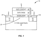
- FIG 1 illustrates a Silicon Carbide (SiC) lateral Metal-Oxide-Semiconductor Field Effect Transistor (MOSFET) 10 (hereinafter "MOSFET 10") according to one embodiment of the present disclosure.
- the MOSFET 10 includes a p-type SiC substrate 12, a first n+ well 14 forming a source region of the MOSFET 10, a second n+ well 16 forming a drain region of the MOSFET 10, and a gate stack 18 arranged as shown.
- the p-type SiC substrate 12 may be of the 4H, 6H, 3C, or 15R polytype.
- a “substrate” may be a bulk substrate, a series of epitaxial layers (i.e., epilayers), or a combination thereof (i.e., a series of one or more epilayers grown on a bulk substrate).
- the gate stack 18 is formed on the surface of the substrate 12 between the source and drain regions such that the gate stack 18 is deposited over a channel region 20 of the MOSFET 10.
- the gate stack 18 includes an interlayer 22 on the surface of the substrate 12 over the channel region 20. Additionally, the gate stack 18 may include a gate oxide 24 on the surface of the interlayer 22 opposite the substrate 12, and a gate contact 26 on the surface of the gate oxide 24 opposite the interlayer 22.
- the interlayer 22 contains an alkaline earth metal.
- the interlayer 22 may be, for example:
- a channel mobility of the MOSFET 10 is substantially greater than that of a conventional SiC MOSFET (e.g., the same SiC MOSFET but without the interlayer 22) without significantly lowering a threshold voltage of the MOSFET 10.
- the channel mobility of the MOSFET 10 is at least two and a half times greater than that of the same MOSFET without the interlayer 22 containing the alkaline earth metal.
- the channel mobility of the MOSFET 10 is at least 50 cm 2 V -1 s -1 for control voltages greater than 3 Volts.
- the channel mobility of the MOSFET 10 is at least 40 cm 2 V -1 s -1 for control voltages greater than 2.5 Volts. In another embodiment, the channel mobility of the MOSFET 10 is at least 60 cm 2 V -1 s -1 for control voltages greater than 4 Volts. In another embodiment, the channel mobility of the MOSFET 10 is in a range of and including 40-75 cm 2 V -1 s -1 for control voltages greater than 2.5 Volts. In another embodiment, the channel mobility of the MOSFET 10 is in a range of and including 50-75 cm 2 V -1 s -1 for control voltages greater than 3 Volts.
- the channel mobility of the MOSFET 10 is at least 50 cm 2 V -1 s -1 for control voltages in a range of and including 3 Volts to 15 Volts.
- the channel mobility of the MOSFET 10 is at least 40 cm 2 V -1 s -1 for control voltages in a range of and including 2.5 Volts to 15 Volts, at least 60 cm 2 V -1 s -1 for control voltages in a range of and including 4 Volts to 15 Volts, in a range of and including 40-75 cm 2 V -1 s -1 for control voltages in a range of and including 2.5 Volts to 15 Volts, and in a range of and including 50-75 cm 2 V -1 s -1 for control voltages in a range of and including 3 Volts to 15 Volts.
- the gate oxide 24 is preferably Silicon Dioxide (SiO 2 ), but is not limited thereto.
- the gate oxide 24 may alternatively be formed of Aluminum Oxide (Al 2 O 3 ), Hafnium Oxide (HfO 2 ), or similar dielectric material.
- a thickness of the gate oxide 24 may vary depending on the particular implementation. As one example, the thickness of the gate oxide 24 is in the range of and including 300 Angstroms to 1000 Angstroms.
- the gate contact 26 is preferably polysilicon, but is not limited thereto.
- the gate contact 26 may alternatively be formed of a metal such as, for example, Aluminum (Al), Platinum (Pt), Molybdenum (Mo), or the like.
- the MOSFET 10 includes a metal source contact 28 formed over the first n+ well 14 to provide a source contact for the MOSFET 10.
- a metal drain contact 30 is formed over the second n+ well 16 to provide a drain contact for the MOSFET 10.
- the metal source and drain contacts 28 and 30 may be formed of, for example, Nickel (Ni), Nickel Silicide (NiSi), Tantalum Disilicide (TaSi 2 ), or the like.
- a positive gate voltage is applied to the gate contact 26 an n-type inversion channel is created between the n+ wells 14 and 16 forming the source and drain regions of the MOSFET 10.
- the gate voltage is greater than a turn-on, or threshold, voltage of the MOSFET 10, current flows from the source region to the drain region of the MOSFET 10.
- FIGS 2A through 2E graphically illustrate an exemplary process for fabricating the MOSFET 10 of Figure 1 according to one embodiment of the present disclosure.
- the process begins with the p-type SiC substrate 12.
- a "substrate” may be a bulk substrate, a series of epitaxial layers, or a combination thereof (i.e., one or more epitaxial layers formed on a bulk substrate).
- the n+ wells 14 and 16 are formed in the substrate 12.
- the n+ wells 14 and 16 may be formed using a conventional technique such as ion implantation.
- the interlayer 22 is formed on, and in this particular embodiment directly on, the surface of the substrate 12, as illustrated in Figure 2C .
- a Ba or BaO layer is deposited on, and preferably directly on, the substrate 12 as the interlayer 22.
- the interlayer 22 may contain other alkaline earth metals such as, for example, Sr.
- the Ba or BaO may be deposited using any suitable technique such as, for example, Molecular Beam Epitaxy (MBE), thermal evaporation, e-beam evaporation, sputtering, Chemical Vapor Deposition (CVD), atomic layer deposition, spin coating, dip coating, ink-jet printing, or the like.
- the thickness of the interlayer 22 is preferably in the range of and including 2 Angstroms to 15 Angstroms. Even more preferably, the thickness of the interlayer 22 is in the range of and including 2 Angstroms to 10 Angstroms.
- the interlayer 22 may be formed via dry or wet chemistry.
- dry chemistry the interlayer 22 is Formed using, for example, one of the following dry chemistry processes:
- the gate oxide 24 is then formed on, and in this embodiment directly on, the surface of the interlayer 22 opposite the substrate 12.
- the gate oxide 24 is SiO 2 having a thickness of approximately 500 Angstroms.
- other dielectric materials may be used.
- the gate oxide 24 may be formed using any suitable technique such as, for example, PECVD, sputter deposition, or electron beam deposition.
- the interlayer 22 and the gate oxide 24 are densified by annealing in oxygen. In one exemplary embodiment, annealing is performed at a temperature of 950 degrees Celsius for 1.5 hours. However, the temperature, time, and ambient used for the annealing process may be varied to optimize device characteristics and to improve reliability as desired for a particular implementation.
- the annealing may result in chemical bonding of elements present in the interlayer 22 and the gate oxide 24.
- the interlayer 22 is initially formed by depositing a Ba or BaO layer, and the gate oxide 24 is SiO 2 such that, after annealing, the interlayer 22 is formed of, or at least includes, Ba X Si Y O Y .
- the gate contact 26 and the metal source and drain contacts 28 and 30 are formed.
- the gate contact 26 may be formed of Molybdenum (Mo) and have a thickness of 35 nanometers.
- Mo Molybdenum
- other gate materials and thicknesses may be used.
- the metal source and drain contacts 28 and 30 are ohmic contacts formed using known ohmic contact formation techniques. More specifically, as an example, a gate contact material is formed on, and in this embodiment directly on, the surface of the gate oxide 24 opposite the interlayer 22. The gate material, the gate oxide 24, and the interlayer 22 are then etched to form the gate stack 18 between the n+ wells 14 and 16. The source and drain contacts 28 and 30 are then formed on the n+ wells 14 and 16, respectively.
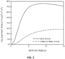
- Figure 3 graphically illustrates the channel mobility of an exemplary embodiment of the MOSFET 10 as compared to that of a conventional SiC MOSFET.
- the channel mobility of the MOSFET 10 is at least approximately two and a half times that of the conventional SiC MOSFET. Further, the channel mobility of the MOSFET 10 is at least 50 cm 2 V -1 s -1 for control voltages greater than 3 Volts.
- the channel mobility of the MOSFET 10 is also at least 40 cm 2 V -1 s -1 for control voltages greater than 2.5 Volts, at least 60 cm 2 V -1 s -1 for control voltages greater than 4 Volts, in a range of and including 40-75 cm 2 V -1 s -1 for control voltages greater than 2.5 Volts, and in a range of and including 50-75 cm 2 V -1 s -1 for control voltages greater than 3 Volts. Still further, the channel mobility of the MOSFET 10 is at least 50 cm 2 V -1 s -1 for control voltages in a range of and including 3 Volts to 15 Volts.
- the channel mobility of the MOSFET 10 is also at least 40 cm 2 V -1 s -1 for control voltages in a range of and including 2.5 Volts to 15 Volts, at least 60 cm 2 V -1 s -1 for control voltages in a range of and including 4 Volts to 15 Volts, in a range of and including 40-75 cm 2 V -1 s -1 for control voltages in a range of and including 2.5 Volts to 15 Volts, and in a range of and including 50-75 cm 2 V -1 s -1 for control voltages in a range of and including 3 Volts to 15 Volts.
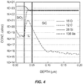
- FIG 4 graphically illustrates elemental depth profiles for one exemplary embodiment of the MOSFET 10 of Figure 1 .
- the elemental depth profiles are more specifically Secondary Ion Mass Spectrometry (SIMS) profiles of various elements in one exemplary embodiment of the gate stack 18 of the MOSFET 10.
- the interlayer 22 contains Ba and is approximately 6 Angstroms thick
- the gate oxide 24 is SiO 2 and is approximately 500 Angstroms thick.
- the vertical lines roughly show the interface between the substrate 12 and the interlayer 22 and the interface between the interlayer 22 and the gate oxide 24.
- MOSFET 10 which is a lateral MOSFET
- present disclosure is not limited thereto.
- MOS devices e.g., vertical MOSFETs, power MOSFETs such as, for example, Double-implanted MOSFETs (DMOSFETs) and U-Shape or trench MOSFETs (UMOSFETs), or the like
- IGBTs Insulated Gate Bipolar Transistors
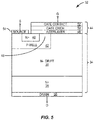
- FIG. 5 illustrates a SiC DMOSFET 32 (hereinafter "DMOSFET 32") according to one embodiment of the present disclosure.
- the DMOSFET 32 is an exemplary vertical MOSFET.
- the DMOSFET 32 includes a SiC substrate 34, which is preferably 4H-SiC.
- the SiC substrate 34 includes a lightly doped n-type drift layer 36 and a heavily doped n-type layer 38.
- the n-type layer 38 forms a drain region of the DMOSFET 32.
- the DMOSFET 32 also includes an n+ source region 40 formed in a p-type well 42, and a gate stack 44 arranged as shown.
- the gate stack 44 is formed over a channel region 46 of the DMOSFET 32 as shown.
- the gate stack 44 is the same as the gate stack 18 of Figure 1 . Specifically, the gate stack 44 includes an interlayer 48 on or directly on the surface of the substrate 34 over the channel region 46, a gate oxide 50 on or directly on the surface of the interlayer 48 opposite the substrate 34, and a gate contact 52 on or directly on the surface of the gate oxide 50 opposite the interlayer 48.
- the interlayer 48 contains an alkaline earth metal.
- the interlayer 48 may be, for example:
- a channel mobility of the DMOSFET 32 is substantially greater than that of a conventional SiC DMOSFET (e.g., the same SiC DMOSFET but without the interlayer 48) without significantly lowering a threshold voltage of the DMOSFET 32.
- the channel mobility of the DMOSFET 32 is at least two and a half times greater than that of the same DMOSFET without the interlayer 48 containing the alkaline earth metal.
- the channel mobility of the DMOSFET 32 is at least 50 cm 2 V -1 s -1 for control voltages greater than 3 Volts.
- the channel mobility of the DMOSFET 32 is at least 40 cm 2 V -1 s -1 for control voltages greater than 2.5 Volts. In another embodiment, the channel mobility of the DMOSFET 32 is at least 60 cm 2 V -1 s -1 for control voltages greater than 4 Volts. In another embodiment, the channel mobility of the DMOSFET 32 is in a range of and including 40-75 cm 2 V -1 s -1 for control voltages greater than 2.5 Volts. In another embodiment, the channel mobility of the DMOSFET 32 is in a range of and including 50-75 cm 2 V -1 s -1 for control voltages greater than 3 Volts.
- the channel mobility of the DMOSFET 32 is at least 50 cm 2 V -1 s -1 for control voltages in a range of and including 3 Volts to 15 Volts.
- the channel mobility of the DMOSFET 32 is at least 40 cm 2 V -1 s -1 for control voltages in a range of and including 2.5 Volts to 15 Volts, at least 60 cm 2 V -1 s -1 for control voltages in a range of and including 4 Volts to 15 Volts, in a range of and including 40-75 cm 2 V -1 s -1 for control voltages in a range of and including 2.5 Volts to 15 Volts, and in a range of and including 50-75 cm 2 V -1 s -1 for control voltages in a range of and including 3 Volts to 15 Volts.
- the gate oxide 50 is preferably SiO 2 , but is not limited thereto.
- the gate oxide 50 may alternatively be formed of Al 2 O 3 , HfO, or similar dielectric material.
- a thickness of the gate oxide 50 may vary depending on the particular implementation. As one example, the thickness of the gate oxide 50 is in the range of and including 300 Angstroms to 1000 Angstroms.
- the gate contact 52 is preferably polysilicon, but is not limited thereto.
- the gate contact 52 may alternatively be formed of a metal such as, for example, Al.
- the DMOSFET 32 includes a metal source contact 54 formed on the source region as illustrated. Likewise, a metal drain contact 56 is formed on a surface of the drain region opposite the drift layer 36 to provide a drain contact for the DMOSFET 32.
- FIG. 6 illustrates an IGBT 58 according to another embodiment of the present disclosure.
- the IGBT 58 includes a SiC substrate 60, which is preferably 4H-SiC.
- the SiC substrate 60 includes a lightly doped n-type drift layer 62 and a highly doped p-type injector layer 64.
- the injector layer 64 may also be referred to herein as a collector region of the IGBT 58.
- the IGBT 58 also includes an n+ source region 66 formed in a p-type well 68, and a gate stack 70 arranged as shown.
- the gate stack 70 is formed over a channel region 72 of the IGBT 58 as shown.
- the gate stack 70 is the same as the gate stack 18 of Figure 1 .
- the gate stack 70 includes an interlayer 74 on or directly on the surface of the substrate 60 over the channel region 72, a gate oxide 76 on or directly on the surface of the interlayer 74 opposite the substrate 60, and a gate contact 78 on or directly on the surface of the gate oxide 76 opposite the interlayer 74.
- the interlayer 74 contains an alkaline earth metal.
- the interlayer 74 may be, for example:
- a channel mobility of the IGBT 58 is substantially greater than that of a conventional SiC IGBT (e.g., the same SiC IGBT but without the interlayer 74) without significantly lowering a threshold voltage of the IGBT 58.
- the channel mobility of the IGBT 58 is at least two and a half times greater than that of the same IGBT without the interlayer 74 containing the alkaline earth metal.
- the channel mobility of the IGBT 58 is at least 50 cm 2 V -1 s -1 for control voltages greater than 3 Volts.
- the channel mobility of the IGBT 58 is at least 40 cm 2 V -1 s -1 for control voltages greater than 2.5 Volts. In another embodiment, the channel mobility of the IGBT 58 is at least 60 cm 2 V -1 s -1 for control voltages greater than 4 Volts. In another embodiment, the channel mobility of the IGBT 58 is in a range of and including 40-75 cm 2 V -1 s -1 for control voltages greater than 2.5 Volts. In another embodiment, the channel mobility of the IGBT 58 is in a range of and including 50-75 cm 2 V -1 s -1 for control voltages greater than 3 Volts.
- the channel mobility of the IGBT 58 is at least 50 cm 2 V -1 s -1 for control voltages in a range of and including 3 Volts to 15 Volts.
- the channel mobility of the IGBT 58 is at least 40 cm 2 V -1 s -1 for control voltages in a range of and including 2.5 Volts to 15 Volts, at least 60 cm 2 V -1 s -1 for control voltages in a range of and including 4 Volts to 15 Volts, in a range of and including 40-75 cm 2 V -1 s -1 for control voltages in a range of and including 2.5 Volts to 15 Volts, and in a range of and including 50-75 cm 2 V -1 s -1 for control voltages in a range of and including 3 Volts to 15 Volts.
- the gate oxide 76 is preferably SiO 2 , but is not limited thereto.
- the gate oxide 76 may alternatively be formed of Al 2 O 3 , HfO, or similar dielectric material.
- a thickness of the gate oxide 76 may vary depending on the particular implementation. As one example, the thickness of the gate oxide 76 is in the range of and including 300 Angstroms to 1000 Angstroms.
- the gate contact 78 is preferably polysilicon, but is not limited thereto.
- the gate contact 78 may alternatively be formed of a metal such as, for example, Al.
- the IGBT 58 includes a metal emitter contact 80 formed over the n+ source region 66 as shown.
- a metal collector contact 82 is formed on a surface of the injector layer 64 opposite the drift layer 62 to provide a collector contact for the IGBT 58.
- FIG. 7 illustrates a trench, or U-shaped, MOSFET 84 according to another embodiment of the present disclosure.
- the MOSFET 84 includes a SiC substrate 86, which is preferably 4H-SiC.
- the SiC substrate 86 includes a highly doped n-type layer 88, a lightly doped n-type drift layer 90, a p-type well 94, and an n+ source region 92 formed in or on the p-type well 94.
- a gate stack 96 is formed in a trench 98 that extends through the n+ source region 92 and the p-type well 94 to the surface of the n-type drift layer 90.
- the gate stack 96 is formed over or adjacent to a channel region 100 of the MOSFET 84 as shown.
- the gate stack 96 is the same as the gate stack 18 of Figure 1 .
- the gate stack 96 includes an interlayer 102 on or directly on the surface of the n-type drift layer 90, on or directly on the sidewalls of the trench 98, and partially on or directly on the surface of the n+ source region 92 on or adjacent to the channel region 100, a gate oxide 104 on or directly on the surface of the interlayer 102, and a gate contact 106 on or directly on the surface of the gate oxide 104 opposite the interlayer 102.
- the interlayer 102 contains an alkaline earth metal.
- the interlayer 102 may be, for example:
- a channel mobility of the MOSFET 84 is substantially greater than that of a conventional SiC trench MOSFET (e.g., the same SiC trench MOSFET but without the interlayer 102) without significantly lowering a threshold voltage of the MOSFET 84.
- the channel mobility of the MOSFET 84 is at least two and a half times greater than that of the same MOSFET without the interlayer 102 containing the alkaline earth metal.
- the channel mobility of the MOSFET 84 is at least 50 cm 2 V -1 s -1 for control voltages greater than 3 Volts.
- the channel mobility of the MOSEFT 84 is at least 40 cm 2 V -1 s -1 for control voltages greater than 2.5 Volts. In another embodiment, the channel mobility of the MOSFET 84 is at least 60 cm 2 V -1 s -1 for control voltages greater than 4 Volts. In another embodiment, the channel mobility of the MOSFET 84 is in a range of and including 40-75 cm 2 V -1 s -1 for control voltages greater than 2.5 Volts. In another embodiment, the channel mobility of the MOSFET 84 is in a range of and including 50-75 cm 2 V -1 s -1 for control voltages greater than 3 Volts.
- the channel mobility of the MOSFET 84 is at least 50 cm 2 V -1 s -1 for control voltages in a range of and including 3 Volts to 15 Volts.
- the channel mobility of the MOSFET 84 is at least 40 cm 2 V -1 s -1 for control voltages in a range of and including 2.5 Volts to 15 Volts, at least 60 cm 2 V -1 s -1 for control voltages in a range of and including 4 Volts to 15 Volts, in a range of and including 40-75 cm 2 V -1 s -1 for control voltages in a range of and including 2.5 Volts to 15 Volts, and in a range of and including 50-75 cm 2 V -1 s -1 for control voltages in a range of and including 3 Volts to 15 Volts.
- the gate oxide 104 is preferably SiO 2 , but is not limited thereto.
- the gate oxide 104 may alternatively be formed of Al 2 O 3 , HfO, or similar dielectric material.
- a thickness of the gate oxide 104 may vary depending on the particular implementation. As one example, the thickness of the gate oxide 104 is in the range of and including 300 Angstroms to 1000 Angstroms.
- the gate contact 106 is preferably polysilicon, but is not limited thereto.
- the gate contact 106 may alternatively be formed of a metal such as, for example, Al.
- the MOSFET 84 includes a metal source contact 108 formed over the n+ source region 92 as shown.
- a metal drain contact 110 is formed on a second surface of the n-type layer 88 opposite the n-type drift layer 90 to provide a drain contact for the MOSFET 84.
- FIG. 8 illustrates a passivation structure 112 for a semiconductor device according to another embodiment of the present disclosure.
- the passivation structure 112 includes an interlayer 114 on or directly on a surface of a substrate 116 (which in this particular example is an n-type drift layer) and a dielectric layer 118 on or directly on a surface of the interlayer 114 opposite the substrate 116.
- the passivation structure 112 is formed over a number of guard rings 120 that, as will be appreciated by one of ordinary skill in the art, provide an edge termination for one or more semiconductor devices formed on the substrate 116.
- the passivation structure 112 is not limited thereto.
- the interlayer 114 contains an alkaline earth metal.
- the interlayer 114 may be, for example:
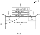
- FIG. 9 illustrates the MOSFET 10 of Figure 1 according to yet another embodiment of the present disclosure.
- the MOSFET 10 is substantially the same as that of Figure 1 .
- the interlayer 22 and the gate oxide 24 are replaced with an alkaline earth metal-oxide-alkaline earth metal structure formed by a first alkaline earth metal (AEM) rich layer 132 on or directly on the substrate 12 over the channel region 20, an oxide layer 134 on or directly on the first AEM rich layer 132 opposite the substrate 12, and a second AEM rich layer 136 on a surface of the oxide layer 134 opposite the first AEM rich layer 132.
- the AEM rich layers 132 and 136 contain the same or different alkaline earth metals.
- Each of the AEM rich layers 132 and 136 may be, for example:
- each of the AEM rich layers 132 and 136 is BaO. In another exemplary embodiment, each of the AEM rich layers 132 and 136 is Ba X Si Y O z .
- the first and second AEM rich layers 132 and 136 may be formed using, for example, any of the dry or wet chemistry processes described above with respect to the interlayer 22 that are suitable for forming the AEM rich layers 132 and 136.
- a channel mobility of the MOSFET 10 is substantially greater than that of a conventional SiC MOSFET (e.g., the same SiC MOSFET but without the alkaline earth metal-oxide-alkaline earth metal structure) without significantly lowering a threshold voltage of the MOSFET 10.
- the channel mobility of the MOSFET 10 is at least two and a half times greater than that of the same MOSFET without the alkaline earth metal-oxide-alkaline earth metal structure.
- the channel mobility of the MOSFET 10 is at least 50 cm 2 V -1 s -1 for control voltages greater than 3 Volts. In another embodiment, the channel mobility of the MOSFET 10 is at least 40 cm 2 V -1 s -1 for control voltages greater than 2.5 Volts. In another embodiment, the channel mobility of the MOSFET 10 is at least 60 cm 2 V -1 s -1 for control voltages greater than 4 Volts. In another embodiment, the channel mobility of the MOSFET 10 is in a range of and including 40-75 cm 2 V -1 s -1 for control voltages greater than 2.5 Volts.
- the channel mobility of the MOSFET 10 is in a range of and including 50-75 cm 2 V -1 s -1 for control voltages greater than 3 Volts. In yet another embodiment, the channel mobility of the MOSFET 10 is at least 50 cm 2 V -1 s -1 for control voltages in a range of and including 3 Volts to 15 Volts.
- the channel mobility of the MOSFET 10 is at least 40 cm 2 V -1 s -1 for control voltages in a range of and including 2.5 Volts to 15 Volts, at least 60 cm 2 V -1 s -1 for control voltages in a range of and including 4 Volts to 15 Volts, in a range of and including 40-75 cm 2 V -1 s -1 for control voltages in a range of and including 2.5 Volts to 15 Volts, and in a range of and including 50-75 cm 2 V -1 s -1 for control voltages in a range of and including 3 Volts to 15 Volts.
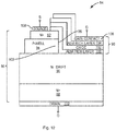
- FIG 10 illustrates the DMOSFET 32 of Figure 5 according to yet another embodiment of the present disclosure.
- the DMOSFET 32 is substantially the same as that of Figure 5 .
- the interlayer 48 and the gate oxide 50 are replaced with an alkaline earth metal-oxide-alkaline earth metal structure formed by a first AEM rich layer 138 on or directly on the substrate 34 over the channel region 46, an oxide layer 140 on or directly on the first AEM rich layer 138 opposite the substrate 34, and a second AEM rich layer 142 on a surface of the oxide layer 140 opposite the first AEM rich layer 138.
- the AEM rich layers 138 and 142 contain the same or different alkaline earth metals.
- Each of the AEM rich layers 138 and 142 may be, for example:
- each of the AEM rich layers 138 and 142 is BaO. In another exemplary embodiment, each of the AEM rich layers 138 and 142 is Ba X Si Y O z .
- the first and second AEM rich layers 138 and 142 may be formed using, for example, any of the dry or wet chemistry processes described above with respect to the interlayer 22 that are suitable for forming the AEM rich layers 138 and 142.
- a channel mobility of the DMOSFET 32 is substantially greater than that of a conventional SiC DMOSFET (e.g., the same SiC DMOSFET but without the alkaline earth metal-oxide-alkaline earth metal structure) without significantly lowering a threshold voltage of the DMOSFET 32.
- the channel mobility of the DMOSFET 32 is at least two and a half times greater than that of the same DMOSFET without the alkaline earth metal-oxide-alkaline earth metal structure.
- the channel mobility of the DMOSFET 32 is at least 50 cm 2 V -1 s -1 for control voltages greater than 3 Volts. In another embodiment, the channel mobility of the DMOSFET 32 is at least 40 cm 2 V -1 s -1 for control voltages greater than 2.5 Volts. In another embodiment, the channel mobility of the DMOSFET 32 is at least 60 cm 2 V -1 s -1 for control voltages greater than 4 Volts. In another embodiment, the channel mobility of the DMOSFET 32 is in a range of and including 40-75 cm 2 V -1 s -1 for control voltages greater than 2.5 Volts.
- the channel mobility of the DMOSFET 32 is in a range of and including 50-75 cm 2 V -1 s -1 for control voltages greater than 3 Volts. In yet another embodiment, the channel mobility of the DMOSFET 32 is at least 50 cm 2 V -1 s -1 for control voltages in a range of and including 3 Volts to 15 Volts.
- the channel mobility of the DMOSFET 32 is at least 40 cm 2 V -1 s -1 for control voltages in a range of and including 2.5 Volts to 15 Volts, at least 60 cm 2 V -1 s -1 for control voltages in a range of and including 4 Volts to 15 Volts, in a range of and including 40-75 cm 2 V -1 s -1 for control voltages in a range of and including 2.5 Volts to 15 Volts, and in a range of and including 50-75 cm 2 V -1 s -1 for control voltages in a range of and including 3 Volts to 15 Volts.
- FIG 11 illustrates the IGBT 58 of Figure 6 according to yet another embodiment of the present disclosure.
- the IGBT 58 is substantially the same as that of Figure 6 .
- the interlayer 74 and the gate oxide 76 are replaced with an alkaline earth metal-oxide-alkaline earth metal structure formed by a first AEM rich layer 144 on or directly on the substrate 60 over the channel region 72, an oxide layer 146 on or directly on the first AEM rich layer 144 opposite the substrate 60, and a second AEM rich layer 148 on a surface of the oxide layer 146 opposite the first AEM rich layer 144.
- the AEM rich layers 144 and 148 contain the same or different alkaline earth metals.
- Each of the AEM rich layers 144 and 148 may be, for example:
- each of the AEM rich layers 144 and 148 is BaO. In another exemplary embodiment, each of the AEM rich layers 144 and 148 is Ba X Si Y O z .
- the first and second AEM rich layers 144 and 148 may be formed using, for example, any of the dry or wet chemistry processes described above with respect to the interlayer 22 that are suitable for forming the AEM rich layers 144 and 148.
- a channel mobility of the IGBT 58 is substantially greater than that of a conventional SiC IGBT (e.g., the same SiC IGBT but without the alkaline earth metal-oxide-alkaline earth metal structure) without significantly lowering a threshold voltage of the IGBT 58.
- the channel mobility of the IGBT 58 is at least two and a half times greater than that of the same IGBT without the alkaline earth metal-oxide-alkaline earth metal structure.
- the channel mobility of the IGBT 58 is at least 50 cm 2 V -1 s -1 for control voltages greater than 3 Volts. In another embodiment, the channel mobility of the IGBT 58 is at least 40 cm 2 V -1 s -1 for control voltages greater than 2.5 Volts. In another embodiment, the channel mobility of the IGBT 58 is at least 60 cm 2 V -1 s -1 for control voltages greater than 4 Volts. In another embodiment, the channel mobility of the IGBT 58 is in a range of and including 40-75 cm 2 V -1 s -1 for control voltages greater than 2.5 Volts.
- the channel mobility of the IGBT 58 is in a range of and including 50-75 cm 2 V -1 s -1 for control voltages greater than 3 Volts. In yet another embodiment, the channel mobility of the IGBT 58 is at least 50 cm 2 V -1 s -1 for control voltages in a range of and including 3 Volts to 15 Volts.
- the channel mobility of the IGBT 58 is at least 40 cm 2 V -1 s -1 for control voltages in a range of and including 2.5 Volts to 15 Volts, at least 60 cm 2 V -1 s -1 for control voltages in a range of and including 4 Volts to 15 Volts, in a range of and including 40-75 cm 2 V -1 s -1 for control voltages in a range of and including 2.5 Volts to 15 Volts, and in a range of and including 50-75 cm 2 V -1 s -1 for control voltages in a range of and including 3 Volts to 15 Volts.
- FIG 12 illustrates the trench, or U-shaped, MOSFET 84 of Figure 7 according to yet another embodiment of the present disclosure.
- the MOSFET 84 is substantially the same as that of Figure 7 .
- the interlayer 102 and the gate oxide 104 are replaced with an alkaline earth metal-oxide-alkaline earth metal structure formed by a first AEM rich layer 150 on or directly on the substrate 86 within the trench 98, an oxide layer 152 on or directly on the first AEM rich layer 150 opposite the substrate 86, and a second AEM rich layer 154 on a surface of the oxide layer 152 opposite the first AEM rich layer 150.
- the AEM rich layers 150 and 154 contain the same or different alkaline earth metals.
- Each of the AEM rich layers 150 and 154 may be, for example:
- each of the AEM rich layers 150 and 154 is BaO. In another exemplary embodiment, each of the AEM rich layers 150 and 154 is Ba X Si Y O z .
- the first and second AEM rich layers 150 and 154 may be formed using, for example, any of the dry or wet chemistry processes described above with respect to the interlayer 22 that are suitable for forming the AEM rich layers 150 and 154.
- a channel mobility of the MOSFET 84 is substantially greater than that of a conventional SiC trench MOSFET (e.g., the same SiC trench MOSFET but without the alkaline earth metal-oxide-alkaline earth metal structure) without significantly lowering a threshold voltage of the MOSFET 84.
- the channel mobility of the MOSFET 84 is at least two and a half times greater than that of the same MOSFET without the alkaline earth metal-oxide-alkaline earth metal structure.
- the channel mobility of the MOSFET 84 is at least 50 cm 2 V -1 s -1 for control voltages greater than 3 Volts. In another embodiment, the channel mobility of the MOSEFT 84 is at least 40 cm 2 V -1 s -1 for control voltages greater than 2.5 Volts. In another embodiment, the channel mobility of the MOSFET 84 is at least 60 cm 2 V -1 s -1 for control voltages greater than 4 Volts. In another embodiment, the channel mobility of the MOSFET 84 is in a range of and including 40-75 cm 2 V -1 s -1 for control voltages greater than 2.5 Volts.
- the channel mobility of the MOSFET 84 is in a range of and including 50-75 cm 2 V -1 s -1 for control voltages greater than 3 Volts. In yet another embodiment, the channel mobility of the MOSFET 84 is at least 50 cm 2 V -1 s -1 for control voltages in a range of and including 3 Volts to 15 Volts.
- the channel mobility of the MOSFET 84 is at least 40 cm 2 V -1 s -1 for control voltages in a range of and including 2.5 Volts to 15 Volts, at least 60 cm 2 V -1 s -1 for control voltages in a range of and including 4 Volts to 15 Volts, in a range of and including 40-75 cm 2 V -1 s -1 for control voltages in a range of and including 2.5 Volts to 15 Volts, and in a range of and including 50-75 cm 2 V -1 s -1 for control voltages in a range of and including 3 Volts to 15 Volts.
- FIG 13 illustrates the passivation structure 112 of Figure 8 according to yet another embodiment of the present disclosure.
- the passivation structure 112 includes an alkaline earth metal-oxide-alkaline earth metal structure formed by a first AEM rich layer 156 on or directly on the substrate 116, an oxide layer 158 on or directly on the first AEM rich layer 156 opposite the substrate 116, and a second AEM rich layer 160 on a surface of the oxide layer 158 opposite the first AEM rich layer 156.
- the AEM rich layers 156 and 160 contain the same or different alkaline earth metals.
- Each of the AEM rich layers 156 and 160 may be, for example:
- semiconductor devices specifically illustrated and described herein are exemplary.
- One of ordinary skill in the art will recognize numerous variations to the illustrated semiconductor devices as well as other types of semiconductor devices to which the disclosed gate, or control contact, stack is applicable. These variations and additional semiconductor devices are considered to be within the scope of the present disclosure.
- the specific devices illustrated herein are n-channel devices, the concepts described herein are equally applicable to p-channel devices.
- the disclosed gate, or control contact, stack can also be used with similar p-channel devices (e.g., a p-channel MOSFET or a p-channel IGBT).
Landscapes
- Insulated Gate Type Field-Effect Transistor (AREA)
- Electrodes Of Semiconductors (AREA)
- Metal-Oxide And Bipolar Metal-Oxide Semiconductor Integrated Circuits (AREA)
- Formation Of Insulating Films (AREA)
Claims (14)
- Halbleitervorrichtung (10), die Folgendes umfasst:ein Siliziumkarbidsubstrat (12), das eine Kanalzone (20) umfasst; undeinen Gate-Stapel (18) auf dem Siliziumkarbidsubstrat auf der Kanalzone, wobei der Gate-Stapel Folgendes umfasst:eine oder mehrere Oxidschichten (132), die Bariumsilikat oder Bariumoxid umfassen;eine dielektrische Schicht (134) auf der einen oder den mehreren Oxidschichten; undeine Gate-Kontaktschicht (26) auf der dielektrischen Schicht.
- Halbleitervorrichtung nach Anspruch 1, wobei die dielektrische Schicht eine Oxidschicht ist und der Gate-Stapel ferner Folgendes umfasst:eine erdalkalimetallreiche Schicht (136) auf der dielektrischen Schicht; unddie Gate-Kontaktschicht (26) auf der erdalkalimetallreichen Schicht gegenüber der dielektrischen Schicht.
- Halbleitervorrichtung nach Anspruch 1, wobei:
die dielektrische Schicht eine Oxidschicht umfasst, die aus einer Gruppe besteht, die aus Folgendem besteht:Siliziumdioxid (SiO2), Aluminiumoxid (Al2O3) und Hafniumoxid (HfO); unddie eine oder die mehreren Oxidschichten direkt auf einer Oberfläche des Siliziumkarbidsubstrats in der Kanalzone liegen. - Halbleitervorrichtung nach Anspruch 1, wobei die Halbleitervorrichtung ein lateraler Metalloxid-Halbleiter-Feldeffekttransistor (metal-oxide-semiconductor field-effect transistor - MOSFET) (10) ist, der ferner Folgendes umfasst:eine Source-Zone (14), die in dem Siliziumkarbidsubstrat ausgebildet ist; undeine Drain-Zone (16), die in dem Siliziumkarbidsubstrat ausgebildet ist;wobei der Gate-Stapel auf dem Siliziumkarbidsubstrat zwischen der Source- und der Drain-Zone ausgebildet ist.
- Halbleitervorrichtung nach Anspruch 1, wobei die Halbleitervorrichtung ein vertikaler Metalloxid-Halbleiter-Feldeffekttransistor (MOSFET) (32) ist, der ferner Folgendes umfasst:eine Senke (42) einer ersten Leitfähigkeitsart, die in dem Siliziumkarbidsubstrat ausgebildet ist, wobei das Siliziumkarbidsubstrat aus einer zweiten Leitfähigkeitsart besteht;eine Source-Zone (40) der zweiten Leitfähigkeitsart, die in der Senke ausgebildet ist,wobei der Gate-Stapel auf dem Siliziumkarbidsubstrat liegt und sich auf wenigstens einem Abschnitt der Senke und der Source-Zone erstreckt; undein Drain-Kontakt (56) auf einer Oberfläche des Siliziumkarbidsubstrats gegenüber dem Gate-Stapel.
- Halbleitervorrichtung nach Anspruch 1, wobei die Halbleitervorrichtung ein Bipolartransistor mit isolierter Gate-Elektrode (insulated-gate bipolar transistor- IGBT) (58) ist, der ferner Folgendes umfasst:eine Emitterzone (66), die in dem Siliziumkarbidsubstrat ausgebildet ist, wobei der Gate-Stapel auf dem Siliziumkarbidsubstrat liegt und sich auf wenigstens einem Abschnitt der Emitterzone erstreckt; undeinen Kollektorkontakt (82) auf einer Oberfläche des Siliziumkarbidsubstrats gegenüber dem Gate-Stapel.
- Halbleitervorrichtung nach Anspruch 1, wobei die Halbleitervorrichtung ein Grabenfeldeffekttransistor (84) ist und:
das Siliziumkarbidsubstrat Folgendes umfasst:eine erste Schicht (88) einer ersten Leitfähigkeitsart;eine Driftschicht (90) der ersten Leitfähigkeitsart auf einer ersten Oberfläche der ersten Schicht der ersten Leitfähigkeitsart;eine Senke (94) einer zweiten Leitfähigkeitsart auf einer Oberfläche der Driftschicht gegenüber der ersten Schicht;eine Source-Zone (92) der ersten Leitfähigkeitsart in oder auf der Senke;einen Source-Kontakt (108) auf einer Oberfläche der Source-Zone gegenüber der Senke;einen Drain-Kontakt (110) auf einer zweiten Oberfläche der ersten Schicht gegenüber der Driftschicht; undeinen Graben (98), der sich von der Oberfläche der Source-Zone durch die Senke zu der Oberfläche der Driftschicht erstreckt, wobei der Gate-Stapel in dem Graben ausgebildet ist. - Halbleitervorrichtung nach den Ansprüchen 4-7, wobei das Siliziumkarbidsubstrat zu einer Gruppe gehört, die aus Folgendem besteht: einem 4H-Siliziumkarbid(SiC)-Substrat, einem 6H-SiC-Substrat, einem 3C-SiC-Substrat und einem 15R-SiC-Substrat.
- Halbleitervorrichtung nach Anspruch 1, wobei eine Dicke der dielektrischen Schicht in einem Bereich von einschließlich 300 bis 1000 Angström liegt und die Halbleitervorrichtung eine Leistungsvorrichtung ist.
- Halbleitervorrichtung nach Anspruch 1, wobei die eine oder die mehreren Oxidschichten eine Zwischenschicht direkt auf dem Siliziumkarbidsubstrat in der Kanalzone sind.
- Verfahren zum Herstellen einer Halbleitervorrichtung, das Folgendes umfasst:Bereitstellen eines Siliziumkarbidsubstrats (12), das eine Kanalzone (20) umfasst; undAusbilden eines Gate-Stapels durch Folgendes:Abscheiden eines Erdalkalimetalls auf der Kanalzone des Siliziumkarbidsubstrats;Oxidieren des Erdalkalimetalls;Tempern des Erdalkalimetalls nach dem Oxidieren des Erdalkalimetalls, wobei dadurch eine erdalkalimetallreiche Schicht ausgebildet wird;Bereitstellen einer dielektrischen Schicht (24, 134) auf der erdalkalimetallreichen Schicht; undBereitstellen einer Gate-Kontaktschicht (26) auf der dielektrischen Schicht.
- Verfahren für die Herstellung nach Anspruch 11, wobei das Ausbilden der erdalkalimetallreichen Schicht auf der Kanalzone das Ausbilden einer ersten erdalkalimetallreichen Schicht direkt auf einer Oberfläche des Siliziumkarbidsubstrats umfasst.
- Verfahren für die Herstellung nach Anspruch 11, wobei die Halbleitervorrichtung ein vertikaler Metalloxid-Halbleiter-Feldeffekttransistor (MOSFET) ist und das Verfahren ferner Folgendes umfasst:Bereitstellen einer Senke einer ersten Leitfähigkeitsart, die in dem Siliziumkarbidsubstrat ausgebildet ist, wobei das Siliziumkarbidsubstrat aus einer zweiten Leitfähigkeitsart besteht;Bereitstellen einer Source-Zone der zweiten Leitfähigkeitsart, die in dem Siliziumkarbidsubstrat ausgebildet ist, wobei der Gate-Stapel auf dem Siliziumkarbidsubstrat liegt und sich über wenigstens einen Abschnitt der Senke und der Source-Zone erstreckt; undBereitstellen eines Drain-Kontakts auf einer Oberfläche des Siliziumkarbidsubstrats gegenüber der erdalkalimetallreichen Schicht, wobei das Siliziumkarbidsubstrat zu einer Gruppe gehört, die aus Folgendem besteht: einem 4H-Siliziumkarbid(SiC)-Substrat, einem 6H-SiC-Substrat, einem 3C-SiC-Substrat und einem 15R-SiC-Substrat.
- Verfahren für die Herstellung nach Anspruch 11, wobei die erdalkalimetallreichen Schicht Bariumsilikat umfasst.
Applications Claiming Priority (4)
| Application Number | Priority Date | Filing Date | Title |
|---|---|---|---|
| US201161501460P | 2011-06-27 | 2011-06-27 | |
| US13/229,266 US9396946B2 (en) | 2011-06-27 | 2011-09-09 | Wet chemistry processes for fabricating a semiconductor device with increased channel mobility |
| EP12741411.8A EP2724363B1 (de) | 2011-06-27 | 2012-06-26 | Nasschemieverfahren zur herstellung einer halbleitenden vorrichtung mit erhöhter kanalmobilität |
| PCT/US2012/044199 WO2013003348A1 (en) | 2011-06-27 | 2012-06-26 | Wet chemistry processes for fabricating a semiconductor device with increased channel mobility |
Related Parent Applications (2)
| Application Number | Title | Priority Date | Filing Date |
|---|---|---|---|
| EP12741411.8A Division-Into EP2724363B1 (de) | 2011-06-27 | 2012-06-26 | Nasschemieverfahren zur herstellung einer halbleitenden vorrichtung mit erhöhter kanalmobilität |
| EP12741411.8A Division EP2724363B1 (de) | 2011-06-27 | 2012-06-26 | Nasschemieverfahren zur herstellung einer halbleitenden vorrichtung mit erhöhter kanalmobilität |
Publications (2)
| Publication Number | Publication Date |
|---|---|
| EP3352201A1 EP3352201A1 (de) | 2018-07-25 |
| EP3352201B1 true EP3352201B1 (de) | 2020-11-18 |
Family
ID=47361010
Family Applications (2)
| Application Number | Title | Priority Date | Filing Date |
|---|---|---|---|
| EP12741411.8A Active EP2724363B1 (de) | 2011-06-27 | 2012-06-26 | Nasschemieverfahren zur herstellung einer halbleitenden vorrichtung mit erhöhter kanalmobilität |
| EP18155888.3A Active EP3352201B1 (de) | 2011-06-27 | 2012-06-26 | Siliziumkarbid-halbleiterbauelement mit erhöhter kanalmobilität |
Family Applications Before (1)
| Application Number | Title | Priority Date | Filing Date |
|---|---|---|---|
| EP12741411.8A Active EP2724363B1 (de) | 2011-06-27 | 2012-06-26 | Nasschemieverfahren zur herstellung einer halbleitenden vorrichtung mit erhöhter kanalmobilität |
Country Status (7)
| Country | Link |
|---|---|
| US (2) | US9396946B2 (de) |
| EP (2) | EP2724363B1 (de) |
| JP (2) | JP5997767B2 (de) |
| KR (2) | KR101600721B1 (de) |
| CN (2) | CN103930973B (de) |
| TW (2) | TWI501322B (de) |
| WO (1) | WO2013003348A1 (de) |
Families Citing this family (25)
| Publication number | Priority date | Publication date | Assignee | Title |
|---|---|---|---|---|
| IN2015KN00665A (de) | 2012-09-07 | 2015-07-17 | Avery Dennison Corp | |
| JP6168945B2 (ja) * | 2013-09-20 | 2017-07-26 | 株式会社東芝 | 半導体装置およびその製造方法 |
| US9111919B2 (en) | 2013-10-03 | 2015-08-18 | Cree, Inc. | Field effect device with enhanced gate dielectric structure |
| JP6189261B2 (ja) * | 2014-07-07 | 2017-08-30 | 株式会社東芝 | 半導体装置およびその製造方法 |
| US10910481B2 (en) * | 2014-11-05 | 2021-02-02 | Cree, Inc. | Semiconductor device with improved insulated gate |
| JP6526549B2 (ja) * | 2015-03-24 | 2019-06-05 | 株式会社東芝 | 半導体装置、インバータ回路、駆動装置、車両、及び、昇降機 |
| JP6552950B2 (ja) * | 2015-03-24 | 2019-07-31 | 株式会社東芝 | 半導体装置、半導体装置の製造方法、インバータ回路、駆動装置、車両、及び、昇降機 |
| US9673315B2 (en) | 2015-03-24 | 2017-06-06 | Kabushiki Kaisha Toshiba | Semiconductor device, inverter circuit, driving device, vehicle, and elevator |
| JP6667809B2 (ja) * | 2016-05-30 | 2020-03-18 | 株式会社東芝 | 半導体装置、インバータ回路、駆動装置、車両、及び、昇降機 |
| JP6606020B2 (ja) * | 2016-06-15 | 2019-11-13 | 株式会社東芝 | 半導体装置、インバータ回路、駆動装置、車両、及び、昇降機 |
| CN107863392A (zh) * | 2016-09-22 | 2018-03-30 | 中兴通讯股份有限公司 | 一种SiC MOS电容及其制造方法 |
| CN107871781A (zh) * | 2016-09-27 | 2018-04-03 | 西安电子科技大学 | 一种碳化硅mosfet及其制造方法 |
| JP6844228B2 (ja) * | 2016-12-02 | 2021-03-17 | 富士電機株式会社 | 半導体装置および半導体装置の製造方法 |
| CN109037332A (zh) * | 2017-06-12 | 2018-12-18 | 中兴通讯股份有限公司 | 碳化硅金属氧化物半导体场效应晶体管及其制造方法 |
| JP6367434B2 (ja) * | 2017-06-21 | 2018-08-01 | 株式会社東芝 | 半導体装置およびその製造方法 |
| US10497777B2 (en) | 2017-09-08 | 2019-12-03 | Hestia Power Inc. | Semiconductor power device |
| US10276704B1 (en) * | 2017-10-17 | 2019-04-30 | Mitsubishi Electric Research Laboratiories, Inc. | High electron mobility transistor with negative capacitor gate |
| KR20200125582A (ko) * | 2018-03-02 | 2020-11-04 | 미쯔비시 가스 케미칼 컴파니, 인코포레이티드 | 알루미나의 보호액, 보호방법 및 이것을 이용한 알루미나층을 가지는 반도체 기판의 제조방법 |
| CN110120425B (zh) * | 2019-05-22 | 2020-08-11 | 西安电子科技大学 | 垂直型的高压mosfet器件及制作方法 |
| JP7388020B2 (ja) * | 2019-07-11 | 2023-11-29 | 富士電機株式会社 | 絶縁ゲート型半導体装置 |
| CN112466756A (zh) * | 2020-11-17 | 2021-03-09 | 深圳宝铭微电子有限公司 | 一种碳化硅mosfet制造方法 |
| CN114551600A (zh) * | 2022-02-22 | 2022-05-27 | 苏州龙驰半导体科技有限公司 | 半导体器件的制作方法和半导体器件 |
| JP2025531221A (ja) * | 2022-09-16 | 2025-09-19 | ヒタチ・エナジー・リミテッド | SiC MOSFETにおけるチャネル移動度を向上させる方法 |
| TWI835394B (zh) * | 2022-11-08 | 2024-03-11 | 財團法人工業技術研究院 | 半導體元件 |
| DE102023206109B4 (de) * | 2023-06-28 | 2026-02-19 | Infineon Technologies Ag | Siliziumcarbidvorrichtung und herstellungsverfahren |
Family Cites Families (57)
| Publication number | Priority date | Publication date | Assignee | Title |
|---|---|---|---|---|
| US4499147A (en) * | 1981-12-28 | 1985-02-12 | Ibiden Co., Ltd. | Silicon carbide substrates and a method of producing the same |
| US5918132A (en) | 1996-12-31 | 1999-06-29 | Intel Corporation | Method for narrow space formation and self-aligned channel implant |
| US7115461B2 (en) | 1997-07-24 | 2006-10-03 | Texas Instruments Incorporated | High permittivity silicate gate dielectric |
| JPH11135774A (ja) | 1997-07-24 | 1999-05-21 | Texas Instr Inc <Ti> | 高誘電率シリケート・ゲート誘電体 |
| US6841439B1 (en) * | 1997-07-24 | 2005-01-11 | Texas Instruments Incorporated | High permittivity silicate gate dielectric |
| US20010013629A1 (en) * | 1998-06-30 | 2001-08-16 | Gang Bai | Multi-layer gate dielectric |
| US6972436B2 (en) | 1998-08-28 | 2005-12-06 | Cree, Inc. | High voltage, high temperature capacitor and interconnection structures |
| US6246076B1 (en) | 1998-08-28 | 2001-06-12 | Cree, Inc. | Layered dielectric on silicon carbide semiconductor structures |
| JP2000106428A (ja) | 1998-09-28 | 2000-04-11 | Toshiba Corp | 半導体装置 |
| JP2000150875A (ja) | 1998-11-13 | 2000-05-30 | Toshiba Corp | 半導体装置及び薄膜形成方法 |
| US6241821B1 (en) * | 1999-03-22 | 2001-06-05 | Motorola, Inc. | Method for fabricating a semiconductor structure having a crystalline alkaline earth metal oxide interface with silicon |
| KR20000066800A (ko) * | 1999-04-21 | 2000-11-15 | 김영환 | 정전기방전 보호소자가 구비된 반도체장치의 레이아웃 |
| TW468212B (en) | 1999-10-25 | 2001-12-11 | Motorola Inc | Method for fabricating a semiconductor structure including a metal oxide interface with silicon |
| US6537613B1 (en) * | 2000-04-10 | 2003-03-25 | Air Products And Chemicals, Inc. | Process for metal metalloid oxides and nitrides with compositional gradients |
| AU2001257346A1 (en) * | 2000-05-31 | 2001-12-11 | Motorola, Inc. | Semiconductor device and method for manufacturing the same |
| KR100697714B1 (ko) | 2000-07-11 | 2007-03-21 | 프리스케일 세미컨덕터, 인크. | Si 기판 위에 결정형 알칼리 토금속 산화물을 제조하는방법 |
| US20020030181A1 (en) | 2000-09-11 | 2002-03-14 | Stroud Eric M. | Chemical solvent for opaque coatings on scratch-off game tickets |
| CA2360312A1 (en) * | 2000-10-30 | 2002-04-30 | National Research Council Of Canada | Novel gate dielectric |
| AU2002213173A1 (en) * | 2000-11-14 | 2002-05-27 | Motorola, Inc. | Semiconductor structure having high dielectric constant material |
| JP2002184973A (ja) | 2000-12-11 | 2002-06-28 | Hitachi Ltd | 半導体装置及びその製造方法 |
| US20020089023A1 (en) * | 2001-01-05 | 2002-07-11 | Motorola, Inc. | Low leakage current metal oxide-nitrides and method of fabricating same |
| US6713846B1 (en) * | 2001-01-26 | 2004-03-30 | Aviza Technology, Inc. | Multilayer high κ dielectric films |
| US7371633B2 (en) | 2001-02-02 | 2008-05-13 | Samsung Electronics Co., Ltd. | Dielectric layer for semiconductor device and method of manufacturing the same |
| JP2002299338A (ja) | 2001-04-03 | 2002-10-11 | Matsushita Electric Ind Co Ltd | 薄膜形成方法及び半導体装置の製造方法 |
| JP3773448B2 (ja) * | 2001-06-21 | 2006-05-10 | 松下電器産業株式会社 | 半導体装置 |
| US6511876B2 (en) * | 2001-06-25 | 2003-01-28 | International Business Machines Corporation | High mobility FETS using A1203 as a gate oxide |
| US20040012043A1 (en) * | 2002-07-17 | 2004-01-22 | Gealy F. Daniel | Novel dielectric stack and method of making same |
| JP3845616B2 (ja) | 2002-12-27 | 2006-11-15 | 株式会社東芝 | 電界効果トランジスタ及びその製造方法 |
| US7183186B2 (en) | 2003-04-22 | 2007-02-27 | Micro Technology, Inc. | Atomic layer deposited ZrTiO4 films |
| JP2005135974A (ja) | 2003-10-28 | 2005-05-26 | Seiko Epson Corp | 絶縁膜の形成方法、並びに圧電体デバイス、強誘電体デバイス、及び電子機器 |
| US7053425B2 (en) * | 2003-11-12 | 2006-05-30 | General Electric Company | Gas sensor device |
| WO2005050777A2 (en) | 2003-11-18 | 2005-06-02 | Halliburton Energy Services, Inc. | Receiver electronics proximate antenna |
| US7115959B2 (en) | 2004-06-22 | 2006-10-03 | International Business Machines Corporation | Method of forming metal/high-k gate stacks with high mobility |
| GB0423343D0 (en) * | 2004-10-21 | 2004-11-24 | Koninkl Philips Electronics Nv | Metal-oxide-semiconductor device |
| US7667277B2 (en) * | 2005-01-13 | 2010-02-23 | International Business Machines Corporation | TiC as a thermally stable p-metal carbide on high k SiO2 gate stacks |
| US7109079B2 (en) * | 2005-01-26 | 2006-09-19 | Freescale Semiconductor, Inc. | Metal gate transistor CMOS process and method for making |
| US20070001231A1 (en) * | 2005-06-29 | 2007-01-04 | Amberwave Systems Corporation | Material systems for dielectrics and metal electrodes |
| KR100650698B1 (ko) * | 2005-08-02 | 2006-11-27 | 삼성전자주식회사 | 듀얼 게이트를 갖는 반도체 장치의 제조 방법 |
| US7436018B2 (en) * | 2005-08-11 | 2008-10-14 | Micron Technology, Inc. | Discrete trap non-volatile multi-functional memory device |
| US7727904B2 (en) * | 2005-09-16 | 2010-06-01 | Cree, Inc. | Methods of forming SiC MOSFETs with high inversion layer mobility |
| US7521376B2 (en) * | 2005-10-26 | 2009-04-21 | International Business Machines Corporation | Method of forming a semiconductor structure using a non-oxygen chalcogen passivation treatment |
| JP4868910B2 (ja) | 2006-03-30 | 2012-02-01 | 株式会社東芝 | 半導体装置およびその製造方法 |
| US20080017936A1 (en) * | 2006-06-29 | 2008-01-24 | International Business Machines Corporation | Semiconductor device structures (gate stacks) with charge compositions |
| US8106381B2 (en) * | 2006-10-18 | 2012-01-31 | Translucent, Inc. | Semiconductor structures with rare-earths |
| US7531452B2 (en) | 2007-03-30 | 2009-05-12 | Tokyo Electron Limited | Strained metal silicon nitride films and method of forming |
| JP5280670B2 (ja) * | 2007-12-07 | 2013-09-04 | ルネサスエレクトロニクス株式会社 | 半導体装置の製造方法 |
| JP2009152392A (ja) | 2007-12-20 | 2009-07-09 | Fujitsu Microelectronics Ltd | 半導体装置の製造方法及び半導体装置 |
| US7947549B2 (en) | 2008-02-26 | 2011-05-24 | International Business Machines Corporation | Gate effective-workfunction modification for CMOS |
| US7741202B2 (en) * | 2008-08-07 | 2010-06-22 | Tokyo Electron Limited | Method of controlling interface layer thickness in high dielectric constant film structures including growing and annealing a chemical oxide layer |
| JP4768788B2 (ja) | 2008-09-12 | 2011-09-07 | 株式会社東芝 | 半導体装置およびその製造方法 |
| US8044469B2 (en) | 2008-09-19 | 2011-10-25 | Samsung Electronics Co., Ltd. | Semiconductor device and associated methods |
| US7999332B2 (en) * | 2009-05-14 | 2011-08-16 | International Business Machines Corporation | Asymmetric semiconductor devices and method of fabricating |
| JP5592083B2 (ja) * | 2009-06-12 | 2014-09-17 | アイメック | 基板処理方法およびそれを用いた半導体装置の製造方法 |
| US7989902B2 (en) * | 2009-06-18 | 2011-08-02 | International Business Machines Corporation | Scavenging metal stack for a high-k gate dielectric |
| JP5721351B2 (ja) * | 2009-07-21 | 2015-05-20 | ローム株式会社 | 半導体装置 |
| JP5568913B2 (ja) | 2009-07-24 | 2014-08-13 | 株式会社ユーテック | Pzt膜の製造方法及び水蒸気加熱装置 |
| US8232148B2 (en) | 2010-03-04 | 2012-07-31 | International Business Machines Corporation | Structure and method to make replacement metal gate and contact metal |
-
2011
- 2011-09-09 US US13/229,266 patent/US9396946B2/en active Active
- 2011-09-09 US US13/229,276 patent/US9269580B2/en active Active
-
2012
- 2012-06-26 KR KR1020147002125A patent/KR101600721B1/ko active Active
- 2012-06-26 EP EP12741411.8A patent/EP2724363B1/de active Active
- 2012-06-26 CN CN201280041907.1A patent/CN103930973B/zh active Active
- 2012-06-26 CN CN201710685897.XA patent/CN107342318B/zh active Active
- 2012-06-26 JP JP2014518913A patent/JP5997767B2/ja active Active
- 2012-06-26 WO PCT/US2012/044199 patent/WO2013003348A1/en not_active Ceased
- 2012-06-26 EP EP18155888.3A patent/EP3352201B1/de active Active
- 2012-06-26 KR KR1020147015854A patent/KR101660142B1/ko active Active
- 2012-06-27 TW TW101123054A patent/TWI501322B/zh active
- 2012-06-27 TW TW103131034A patent/TWI578405B/zh active
-
2016
- 2016-08-26 JP JP2016165443A patent/JP6255071B2/ja active Active
Non-Patent Citations (1)
| Title |
|---|
| None * |
Also Published As
| Publication number | Publication date |
|---|---|
| EP2724363B1 (de) | 2018-04-04 |
| JP2017022388A (ja) | 2017-01-26 |
| US20120326163A1 (en) | 2012-12-27 |
| US20120329216A1 (en) | 2012-12-27 |
| TW201507035A (zh) | 2015-02-16 |
| CN107342318A (zh) | 2017-11-10 |
| WO2013003348A1 (en) | 2013-01-03 |
| CN103930973B (zh) | 2017-08-29 |
| EP3352201A1 (de) | 2018-07-25 |
| KR101660142B1 (ko) | 2016-09-26 |
| US9269580B2 (en) | 2016-02-23 |
| EP2724363A1 (de) | 2014-04-30 |
| TWI578405B (zh) | 2017-04-11 |
| JP5997767B2 (ja) | 2016-09-28 |
| KR101600721B1 (ko) | 2016-03-07 |
| CN103930973A (zh) | 2014-07-16 |
| TW201306138A (zh) | 2013-02-01 |
| JP2014523131A (ja) | 2014-09-08 |
| CN107342318B (zh) | 2021-02-02 |
| KR20140050015A (ko) | 2014-04-28 |
| JP6255071B2 (ja) | 2017-12-27 |
| US9396946B2 (en) | 2016-07-19 |
| TWI501322B (zh) | 2015-09-21 |
| KR20140085595A (ko) | 2014-07-07 |
Similar Documents
| Publication | Publication Date | Title |
|---|---|---|
| EP2724363B1 (de) | Nasschemieverfahren zur herstellung einer halbleitenden vorrichtung mit erhöhter kanalmobilität | |
| US9812529B2 (en) | Semiconductor device and method for manufacturing the same | |
| US9496365B2 (en) | Semiconductor device and manufacturing method for the same | |
| US9755064B2 (en) | Semiconductor device and method for manufacturing the same | |
| US9478616B2 (en) | Semiconductor device having high performance channel | |
| US9443937B2 (en) | Semiconductor device | |
| US8941120B2 (en) | Semiconductor device and method for manufacturing the same | |
| WO2016181903A1 (ja) | 炭化珪素半導体装置およびその製造方法 | |
| JP2010027833A (ja) | 炭化珪素半導体装置およびその製造方法 | |
| EP3216047B1 (de) | Halbleiterbauelement mit verbessertem isoliertem gate | |
| JP2007019095A (ja) | 半導体装置の製造方法 | |
| JP2003303974A (ja) | 炭化珪素半導体装置 |
Legal Events
| Date | Code | Title | Description |
|---|---|---|---|
| PUAI | Public reference made under article 153(3) epc to a published international application that has entered the european phase |
Free format text: ORIGINAL CODE: 0009012 |
|
| STAA | Information on the status of an ep patent application or granted ep patent |
Free format text: STATUS: THE APPLICATION HAS BEEN PUBLISHED |
|
| AC | Divisional application: reference to earlier application |
Ref document number: 2724363 Country of ref document: EP Kind code of ref document: P |
|
| AK | Designated contracting states |
Kind code of ref document: A1 Designated state(s): AL AT BE BG CH CY CZ DE DK EE ES FI FR GB GR HR HU IE IS IT LI LT LU LV MC MK MT NL NO PL PT RO RS SE SI SK SM TR |
|
| STAA | Information on the status of an ep patent application or granted ep patent |
Free format text: STATUS: REQUEST FOR EXAMINATION WAS MADE |
|
| 17P | Request for examination filed |
Effective date: 20190116 |
|
| RBV | Designated contracting states (corrected) |
Designated state(s): AL AT BE BG CH CY CZ DE DK EE ES FI FR GB GR HR HU IE IS IT LI LT LU LV MC MK MT NL NO PL PT RO RS SE SI SK SM TR |
|
| STAA | Information on the status of an ep patent application or granted ep patent |
Free format text: STATUS: EXAMINATION IS IN PROGRESS |
|
| 17Q | First examination report despatched |
Effective date: 20191217 |
|
| GRAP | Despatch of communication of intention to grant a patent |
Free format text: ORIGINAL CODE: EPIDOSNIGR1 |
|
| STAA | Information on the status of an ep patent application or granted ep patent |
Free format text: STATUS: GRANT OF PATENT IS INTENDED |
|
| RIC1 | Information provided on ipc code assigned before grant |
Ipc: H01L 29/16 20060101ALN20200527BHEP Ipc: H01L 21/314 20060101ALI20200527BHEP Ipc: H01L 21/336 20060101ALI20200527BHEP Ipc: H01L 29/51 20060101ALI20200527BHEP Ipc: H01L 21/331 20060101ALI20200527BHEP Ipc: H01L 21/28 20060101AFI20200527BHEP |
|
| INTG | Intention to grant announced |
Effective date: 20200615 |
|
| GRAS | Grant fee paid |
Free format text: ORIGINAL CODE: EPIDOSNIGR3 |
|
| GRAA | (expected) grant |
Free format text: ORIGINAL CODE: 0009210 |
|
| STAA | Information on the status of an ep patent application or granted ep patent |
Free format text: STATUS: THE PATENT HAS BEEN GRANTED |
|
| AC | Divisional application: reference to earlier application |
Ref document number: 2724363 Country of ref document: EP Kind code of ref document: P |
|
| AK | Designated contracting states |
Kind code of ref document: B1 Designated state(s): AL AT BE BG CH CY CZ DE DK EE ES FI FR GB GR HR HU IE IS IT LI LT LU LV MC MK MT NL NO PL PT RO RS SE SI SK SM TR |
|
| REG | Reference to a national code |
Ref country code: GB Ref legal event code: FG4D |
|
| REG | Reference to a national code |
Ref country code: CH Ref legal event code: EP |
|
| REG | Reference to a national code |
Ref country code: DE Ref legal event code: R096 Ref document number: 602012073350 Country of ref document: DE |
|
| REG | Reference to a national code |
Ref country code: IE Ref legal event code: FG4D |
|
| REG | Reference to a national code |
Ref country code: AT Ref legal event code: REF Ref document number: 1336683 Country of ref document: AT Kind code of ref document: T Effective date: 20201215 |
|
| REG | Reference to a national code |
Ref country code: AT Ref legal event code: MK05 Ref document number: 1336683 Country of ref document: AT Kind code of ref document: T Effective date: 20201118 |
|
| REG | Reference to a national code |
Ref country code: NL Ref legal event code: MP Effective date: 20201118 |
|
| PG25 | Lapsed in a contracting state [announced via postgrant information from national office to epo] |
Ref country code: RS Free format text: LAPSE BECAUSE OF FAILURE TO SUBMIT A TRANSLATION OF THE DESCRIPTION OR TO PAY THE FEE WITHIN THE PRESCRIBED TIME-LIMIT Effective date: 20201118 Ref country code: PT Free format text: LAPSE BECAUSE OF FAILURE TO SUBMIT A TRANSLATION OF THE DESCRIPTION OR TO PAY THE FEE WITHIN THE PRESCRIBED TIME-LIMIT Effective date: 20210318 Ref country code: FI Free format text: LAPSE BECAUSE OF FAILURE TO SUBMIT A TRANSLATION OF THE DESCRIPTION OR TO PAY THE FEE WITHIN THE PRESCRIBED TIME-LIMIT Effective date: 20201118 Ref country code: NO Free format text: LAPSE BECAUSE OF FAILURE TO SUBMIT A TRANSLATION OF THE DESCRIPTION OR TO PAY THE FEE WITHIN THE PRESCRIBED TIME-LIMIT Effective date: 20210218 Ref country code: GR Free format text: LAPSE BECAUSE OF FAILURE TO SUBMIT A TRANSLATION OF THE DESCRIPTION OR TO PAY THE FEE WITHIN THE PRESCRIBED TIME-LIMIT Effective date: 20210219 |
|
| PG25 | Lapsed in a contracting state [announced via postgrant information from national office to epo] |
Ref country code: AT Free format text: LAPSE BECAUSE OF FAILURE TO SUBMIT A TRANSLATION OF THE DESCRIPTION OR TO PAY THE FEE WITHIN THE PRESCRIBED TIME-LIMIT Effective date: 20201118 Ref country code: BG Free format text: LAPSE BECAUSE OF FAILURE TO SUBMIT A TRANSLATION OF THE DESCRIPTION OR TO PAY THE FEE WITHIN THE PRESCRIBED TIME-LIMIT Effective date: 20210218 Ref country code: PL Free format text: LAPSE BECAUSE OF FAILURE TO SUBMIT A TRANSLATION OF THE DESCRIPTION OR TO PAY THE FEE WITHIN THE PRESCRIBED TIME-LIMIT Effective date: 20201118 Ref country code: IS Free format text: LAPSE BECAUSE OF FAILURE TO SUBMIT A TRANSLATION OF THE DESCRIPTION OR TO PAY THE FEE WITHIN THE PRESCRIBED TIME-LIMIT Effective date: 20210318 Ref country code: LV Free format text: LAPSE BECAUSE OF FAILURE TO SUBMIT A TRANSLATION OF THE DESCRIPTION OR TO PAY THE FEE WITHIN THE PRESCRIBED TIME-LIMIT Effective date: 20201118 Ref country code: SE Free format text: LAPSE BECAUSE OF FAILURE TO SUBMIT A TRANSLATION OF THE DESCRIPTION OR TO PAY THE FEE WITHIN THE PRESCRIBED TIME-LIMIT Effective date: 20201118 |
|
| REG | Reference to a national code |
Ref country code: LT Ref legal event code: MG9D |
|
| PG25 | Lapsed in a contracting state [announced via postgrant information from national office to epo] |
Ref country code: HR Free format text: LAPSE BECAUSE OF FAILURE TO SUBMIT A TRANSLATION OF THE DESCRIPTION OR TO PAY THE FEE WITHIN THE PRESCRIBED TIME-LIMIT Effective date: 20201118 |
|
| PG25 | Lapsed in a contracting state [announced via postgrant information from national office to epo] |
Ref country code: RO Free format text: LAPSE BECAUSE OF FAILURE TO SUBMIT A TRANSLATION OF THE DESCRIPTION OR TO PAY THE FEE WITHIN THE PRESCRIBED TIME-LIMIT Effective date: 20201118 Ref country code: SK Free format text: LAPSE BECAUSE OF FAILURE TO SUBMIT A TRANSLATION OF THE DESCRIPTION OR TO PAY THE FEE WITHIN THE PRESCRIBED TIME-LIMIT Effective date: 20201118 Ref country code: SM Free format text: LAPSE BECAUSE OF FAILURE TO SUBMIT A TRANSLATION OF THE DESCRIPTION OR TO PAY THE FEE WITHIN THE PRESCRIBED TIME-LIMIT Effective date: 20201118 Ref country code: LT Free format text: LAPSE BECAUSE OF FAILURE TO SUBMIT A TRANSLATION OF THE DESCRIPTION OR TO PAY THE FEE WITHIN THE PRESCRIBED TIME-LIMIT Effective date: 20201118 Ref country code: CZ Free format text: LAPSE BECAUSE OF FAILURE TO SUBMIT A TRANSLATION OF THE DESCRIPTION OR TO PAY THE FEE WITHIN THE PRESCRIBED TIME-LIMIT Effective date: 20201118 Ref country code: EE Free format text: LAPSE BECAUSE OF FAILURE TO SUBMIT A TRANSLATION OF THE DESCRIPTION OR TO PAY THE FEE WITHIN THE PRESCRIBED TIME-LIMIT Effective date: 20201118 |
|
| REG | Reference to a national code |
Ref country code: DE Ref legal event code: R097 Ref document number: 602012073350 Country of ref document: DE |
|
| PG25 | Lapsed in a contracting state [announced via postgrant information from national office to epo] |
Ref country code: DK Free format text: LAPSE BECAUSE OF FAILURE TO SUBMIT A TRANSLATION OF THE DESCRIPTION OR TO PAY THE FEE WITHIN THE PRESCRIBED TIME-LIMIT Effective date: 20201118 |
|
| PLBE | No opposition filed within time limit |
Free format text: ORIGINAL CODE: 0009261 |
|
| STAA | Information on the status of an ep patent application or granted ep patent |
Free format text: STATUS: NO OPPOSITION FILED WITHIN TIME LIMIT |
|
| 26N | No opposition filed |
Effective date: 20210819 |
|
| PG25 | Lapsed in a contracting state [announced via postgrant information from national office to epo] |
Ref country code: AL Free format text: LAPSE BECAUSE OF FAILURE TO SUBMIT A TRANSLATION OF THE DESCRIPTION OR TO PAY THE FEE WITHIN THE PRESCRIBED TIME-LIMIT Effective date: 20201118 Ref country code: NL Free format text: LAPSE BECAUSE OF FAILURE TO SUBMIT A TRANSLATION OF THE DESCRIPTION OR TO PAY THE FEE WITHIN THE PRESCRIBED TIME-LIMIT Effective date: 20201118 |
|
| PG25 | Lapsed in a contracting state [announced via postgrant information from national office to epo] |
Ref country code: SI Free format text: LAPSE BECAUSE OF FAILURE TO SUBMIT A TRANSLATION OF THE DESCRIPTION OR TO PAY THE FEE WITHIN THE PRESCRIBED TIME-LIMIT Effective date: 20201118 |
|
| PG25 | Lapsed in a contracting state [announced via postgrant information from national office to epo] |
Ref country code: MC Free format text: LAPSE BECAUSE OF FAILURE TO SUBMIT A TRANSLATION OF THE DESCRIPTION OR TO PAY THE FEE WITHIN THE PRESCRIBED TIME-LIMIT Effective date: 20201118 Ref country code: ES Free format text: LAPSE BECAUSE OF FAILURE TO SUBMIT A TRANSLATION OF THE DESCRIPTION OR TO PAY THE FEE WITHIN THE PRESCRIBED TIME-LIMIT Effective date: 20201118 |
|
| REG | Reference to a national code |
Ref country code: CH Ref legal event code: PL |
|
| GBPC | Gb: european patent ceased through non-payment of renewal fee |
Effective date: 20210626 |
|
| REG | Reference to a national code |
Ref country code: BE Ref legal event code: MM Effective date: 20210630 |
|
| PG25 | Lapsed in a contracting state [announced via postgrant information from national office to epo] |
Ref country code: LU Free format text: LAPSE BECAUSE OF NON-PAYMENT OF DUE FEES Effective date: 20210626 |
|
| PG25 | Lapsed in a contracting state [announced via postgrant information from national office to epo] |
Ref country code: LI Free format text: LAPSE BECAUSE OF NON-PAYMENT OF DUE FEES Effective date: 20210630 Ref country code: IE Free format text: LAPSE BECAUSE OF NON-PAYMENT OF DUE FEES Effective date: 20210626 Ref country code: GB Free format text: LAPSE BECAUSE OF NON-PAYMENT OF DUE FEES Effective date: 20210626 Ref country code: CH Free format text: LAPSE BECAUSE OF NON-PAYMENT OF DUE FEES Effective date: 20210630 |
|
| PG25 | Lapsed in a contracting state [announced via postgrant information from national office to epo] |
Ref country code: IS Free format text: LAPSE BECAUSE OF FAILURE TO SUBMIT A TRANSLATION OF THE DESCRIPTION OR TO PAY THE FEE WITHIN THE PRESCRIBED TIME-LIMIT Effective date: 20210318 Ref country code: FR Free format text: LAPSE BECAUSE OF NON-PAYMENT OF DUE FEES Effective date: 20210630 |
|
| PG25 | Lapsed in a contracting state [announced via postgrant information from national office to epo] |
Ref country code: BE Free format text: LAPSE BECAUSE OF NON-PAYMENT OF DUE FEES Effective date: 20210630 |
|
| PG25 | Lapsed in a contracting state [announced via postgrant information from national office to epo] |
Ref country code: CY Free format text: LAPSE BECAUSE OF FAILURE TO SUBMIT A TRANSLATION OF THE DESCRIPTION OR TO PAY THE FEE WITHIN THE PRESCRIBED TIME-LIMIT Effective date: 20201118 |
|
| PG25 | Lapsed in a contracting state [announced via postgrant information from national office to epo] |
Ref country code: HU Free format text: LAPSE BECAUSE OF FAILURE TO SUBMIT A TRANSLATION OF THE DESCRIPTION OR TO PAY THE FEE WITHIN THE PRESCRIBED TIME-LIMIT; INVALID AB INITIO Effective date: 20120626 |
|
| PG25 | Lapsed in a contracting state [announced via postgrant information from national office to epo] |
Ref country code: MK Free format text: LAPSE BECAUSE OF FAILURE TO SUBMIT A TRANSLATION OF THE DESCRIPTION OR TO PAY THE FEE WITHIN THE PRESCRIBED TIME-LIMIT Effective date: 20201118 |
|
| PG25 | Lapsed in a contracting state [announced via postgrant information from national office to epo] |
Ref country code: MT Free format text: LAPSE BECAUSE OF FAILURE TO SUBMIT A TRANSLATION OF THE DESCRIPTION OR TO PAY THE FEE WITHIN THE PRESCRIBED TIME-LIMIT Effective date: 20201118 |
|
| REG | Reference to a national code |
Ref country code: DE Ref legal event code: R079 Ref document number: 602012073350 Country of ref document: DE Free format text: PREVIOUS MAIN CLASS: H01L0021280000 Ipc: H10D0064010000 |
|
| PGFP | Annual fee paid to national office [announced via postgrant information from national office to epo] |
Ref country code: DE Payment date: 20250627 Year of fee payment: 14 |
|
| PGFP | Annual fee paid to national office [announced via postgrant information from national office to epo] |
Ref country code: IT Payment date: 20250619 Year of fee payment: 14 |
|
| PG25 | Lapsed in a contracting state [announced via postgrant information from national office to epo] |
Ref country code: TR Free format text: LAPSE BECAUSE OF FAILURE TO SUBMIT A TRANSLATION OF THE DESCRIPTION OR TO PAY THE FEE WITHIN THE PRESCRIBED TIME-LIMIT Effective date: 20201118 |