EP3258752A1 - Verfahren zur formung einer laminierten leiterplatte und unter verwendung davon laminierte leiterplatte - Google Patents
Verfahren zur formung einer laminierten leiterplatte und unter verwendung davon laminierte leiterplatte Download PDFInfo
- Publication number
- EP3258752A1 EP3258752A1 EP16749345.1A EP16749345A EP3258752A1 EP 3258752 A1 EP3258752 A1 EP 3258752A1 EP 16749345 A EP16749345 A EP 16749345A EP 3258752 A1 EP3258752 A1 EP 3258752A1
- Authority
- EP
- European Patent Office
- Prior art keywords
- circuit
- circuit board
- laminated
- circuit boards
- forming
- Prior art date
- Legal status (The legal status is an assumption and is not a legal conclusion. Google has not performed a legal analysis and makes no representation as to the accuracy of the status listed.)
- Pending
Links
Images


Classifications
-
- H—ELECTRICITY
- H05—ELECTRIC TECHNIQUES NOT OTHERWISE PROVIDED FOR
- H05K—PRINTED CIRCUITS; CASINGS OR CONSTRUCTIONAL DETAILS OF ELECTRIC APPARATUS; MANUFACTURE OF ASSEMBLAGES OF ELECTRICAL COMPONENTS
- H05K3/00—Apparatus or processes for manufacturing printed circuits
- H05K3/36—Assembling printed circuits with other printed circuits
- H05K3/361—Assembling flexible printed circuits with other printed circuits
-
- H—ELECTRICITY
- H05—ELECTRIC TECHNIQUES NOT OTHERWISE PROVIDED FOR
- H05K—PRINTED CIRCUITS; CASINGS OR CONSTRUCTIONAL DETAILS OF ELECTRIC APPARATUS; MANUFACTURE OF ASSEMBLAGES OF ELECTRICAL COMPONENTS
- H05K1/00—Printed circuits
- H05K1/02—Details
- H05K1/11—Printed elements for providing electric connections to or between printed circuits
- H05K1/115—Via connections; Lands around holes or via connections
- H05K1/116—Lands, clearance holes or other lay-out details concerning the surrounding of a via
-
- H—ELECTRICITY
- H05—ELECTRIC TECHNIQUES NOT OTHERWISE PROVIDED FOR
- H05K—PRINTED CIRCUITS; CASINGS OR CONSTRUCTIONAL DETAILS OF ELECTRIC APPARATUS; MANUFACTURE OF ASSEMBLAGES OF ELECTRICAL COMPONENTS
- H05K1/00—Printed circuits
- H05K1/02—Details
- H05K1/11—Printed elements for providing electric connections to or between printed circuits
- H05K1/118—Printed elements for providing electric connections to or between printed circuits specially for flexible printed circuits, e.g. using folded portions
-
- H—ELECTRICITY
- H05—ELECTRIC TECHNIQUES NOT OTHERWISE PROVIDED FOR
- H05K—PRINTED CIRCUITS; CASINGS OR CONSTRUCTIONAL DETAILS OF ELECTRIC APPARATUS; MANUFACTURE OF ASSEMBLAGES OF ELECTRICAL COMPONENTS
- H05K1/00—Printed circuits
- H05K1/02—Details
- H05K1/14—Structural association of two or more printed circuits
- H05K1/144—Stacked arrangements of planar printed circuit boards
-
- H—ELECTRICITY
- H05—ELECTRIC TECHNIQUES NOT OTHERWISE PROVIDED FOR
- H05K—PRINTED CIRCUITS; CASINGS OR CONSTRUCTIONAL DETAILS OF ELECTRIC APPARATUS; MANUFACTURE OF ASSEMBLAGES OF ELECTRICAL COMPONENTS
- H05K3/00—Apparatus or processes for manufacturing printed circuits
- H05K3/36—Assembling printed circuits with other printed circuits
- H05K3/361—Assembling flexible printed circuits with other printed circuits
- H05K3/363—Assembling flexible printed circuits with other printed circuits by soldering
-
- H—ELECTRICITY
- H05—ELECTRIC TECHNIQUES NOT OTHERWISE PROVIDED FOR
- H05K—PRINTED CIRCUITS; CASINGS OR CONSTRUCTIONAL DETAILS OF ELECTRIC APPARATUS; MANUFACTURE OF ASSEMBLAGES OF ELECTRICAL COMPONENTS
- H05K3/00—Apparatus or processes for manufacturing printed circuits
- H05K3/40—Forming printed elements for providing electric connections to or between printed circuits
- H05K3/403—Edge contacts; Windows or holes in the substrate having plural connections on the walls thereof
-
- H—ELECTRICITY
- H05—ELECTRIC TECHNIQUES NOT OTHERWISE PROVIDED FOR
- H05K—PRINTED CIRCUITS; CASINGS OR CONSTRUCTIONAL DETAILS OF ELECTRIC APPARATUS; MANUFACTURE OF ASSEMBLAGES OF ELECTRICAL COMPONENTS
- H05K3/00—Apparatus or processes for manufacturing printed circuits
- H05K3/40—Forming printed elements for providing electric connections to or between printed circuits
- H05K3/4038—Through-connections; Vertical interconnect access [VIA] connections
-
- H—ELECTRICITY
- H05—ELECTRIC TECHNIQUES NOT OTHERWISE PROVIDED FOR
- H05K—PRINTED CIRCUITS; CASINGS OR CONSTRUCTIONAL DETAILS OF ELECTRIC APPARATUS; MANUFACTURE OF ASSEMBLAGES OF ELECTRICAL COMPONENTS
- H05K3/00—Apparatus or processes for manufacturing printed circuits
- H05K3/46—Manufacturing multilayer circuits
- H05K3/4611—Manufacturing multilayer circuits by laminating two or more circuit boards
- H05K3/4623—Manufacturing multilayer circuits by laminating two or more circuit boards the circuit boards having internal via connections between two or more circuit layers before lamination, e.g. double-sided circuit boards
-
- H—ELECTRICITY
- H05—ELECTRIC TECHNIQUES NOT OTHERWISE PROVIDED FOR
- H05K—PRINTED CIRCUITS; CASINGS OR CONSTRUCTIONAL DETAILS OF ELECTRIC APPARATUS; MANUFACTURE OF ASSEMBLAGES OF ELECTRICAL COMPONENTS
- H05K3/00—Apparatus or processes for manufacturing printed circuits
- H05K3/46—Manufacturing multilayer circuits
- H05K3/4611—Manufacturing multilayer circuits by laminating two or more circuit boards
- H05K3/4626—Manufacturing multilayer circuits by laminating two or more circuit boards characterised by the insulating layers or materials
- H05K3/4635—Manufacturing multilayer circuits by laminating two or more circuit boards characterised by the insulating layers or materials laminating flexible circuit boards using additional insulating adhesive materials between the boards
-
- H—ELECTRICITY
- H05—ELECTRIC TECHNIQUES NOT OTHERWISE PROVIDED FOR
- H05K—PRINTED CIRCUITS; CASINGS OR CONSTRUCTIONAL DETAILS OF ELECTRIC APPARATUS; MANUFACTURE OF ASSEMBLAGES OF ELECTRICAL COMPONENTS
- H05K3/00—Apparatus or processes for manufacturing printed circuits
- H05K3/46—Manufacturing multilayer circuits
- H05K3/4688—Composite multilayer circuits, i.e. comprising insulating layers having different properties
- H05K3/4691—Rigid-flexible multilayer circuits comprising rigid and flexible layers, e.g. having in the bending regions only flexible layers
-
- H—ELECTRICITY
- H05—ELECTRIC TECHNIQUES NOT OTHERWISE PROVIDED FOR
- H05K—PRINTED CIRCUITS; CASINGS OR CONSTRUCTIONAL DETAILS OF ELECTRIC APPARATUS; MANUFACTURE OF ASSEMBLAGES OF ELECTRICAL COMPONENTS
- H05K1/00—Printed circuits
- H05K1/02—Details
- H05K1/0277—Bendability or stretchability details
- H05K1/028—Bending or folding regions of flexible printed circuits
-
- H—ELECTRICITY
- H05—ELECTRIC TECHNIQUES NOT OTHERWISE PROVIDED FOR
- H05K—PRINTED CIRCUITS; CASINGS OR CONSTRUCTIONAL DETAILS OF ELECTRIC APPARATUS; MANUFACTURE OF ASSEMBLAGES OF ELECTRICAL COMPONENTS
- H05K1/00—Printed circuits
- H05K1/02—Details
- H05K1/03—Use of materials for the substrate
- H05K1/0393—Flexible materials
-
- H—ELECTRICITY
- H05—ELECTRIC TECHNIQUES NOT OTHERWISE PROVIDED FOR
- H05K—PRINTED CIRCUITS; CASINGS OR CONSTRUCTIONAL DETAILS OF ELECTRIC APPARATUS; MANUFACTURE OF ASSEMBLAGES OF ELECTRICAL COMPONENTS
- H05K2201/00—Indexing scheme relating to printed circuits covered by H05K1/00
- H05K2201/04—Assemblies of printed circuits
- H05K2201/041—Stacked PCBs, i.e. having neither an empty space nor mounted components in between
-
- H—ELECTRICITY
- H05—ELECTRIC TECHNIQUES NOT OTHERWISE PROVIDED FOR
- H05K—PRINTED CIRCUITS; CASINGS OR CONSTRUCTIONAL DETAILS OF ELECTRIC APPARATUS; MANUFACTURE OF ASSEMBLAGES OF ELECTRICAL COMPONENTS
- H05K2201/00—Indexing scheme relating to printed circuits covered by H05K1/00
- H05K2201/05—Flexible printed circuits [FPCs]
- H05K2201/058—Direct connection between two or more FPCs or between flexible parts of rigid PCBs
-
- H—ELECTRICITY
- H05—ELECTRIC TECHNIQUES NOT OTHERWISE PROVIDED FOR
- H05K—PRINTED CIRCUITS; CASINGS OR CONSTRUCTIONAL DETAILS OF ELECTRIC APPARATUS; MANUFACTURE OF ASSEMBLAGES OF ELECTRICAL COMPONENTS
- H05K2201/00—Indexing scheme relating to printed circuits covered by H05K1/00
- H05K2201/09—Shape and layout
- H05K2201/09145—Edge details
- H05K2201/09181—Notches in edge pads
-
- H—ELECTRICITY
- H05—ELECTRIC TECHNIQUES NOT OTHERWISE PROVIDED FOR
- H05K—PRINTED CIRCUITS; CASINGS OR CONSTRUCTIONAL DETAILS OF ELECTRIC APPARATUS; MANUFACTURE OF ASSEMBLAGES OF ELECTRICAL COMPONENTS
- H05K2201/00—Indexing scheme relating to printed circuits covered by H05K1/00
- H05K2201/09—Shape and layout
- H05K2201/09818—Shape or layout details not covered by a single group of H05K2201/09009 - H05K2201/09809
- H05K2201/09845—Stepped hole, via, edge, bump or conductor
-
- H—ELECTRICITY
- H05—ELECTRIC TECHNIQUES NOT OTHERWISE PROVIDED FOR
- H05K—PRINTED CIRCUITS; CASINGS OR CONSTRUCTIONAL DETAILS OF ELECTRIC APPARATUS; MANUFACTURE OF ASSEMBLAGES OF ELECTRICAL COMPONENTS
- H05K2201/00—Indexing scheme relating to printed circuits covered by H05K1/00
- H05K2201/10—Details of components or other objects attached to or integrated in a printed circuit board
- H05K2201/10007—Types of components
- H05K2201/10121—Optical component, e.g. opto-electronic component
-
- H—ELECTRICITY
- H05—ELECTRIC TECHNIQUES NOT OTHERWISE PROVIDED FOR
- H05K—PRINTED CIRCUITS; CASINGS OR CONSTRUCTIONAL DETAILS OF ELECTRIC APPARATUS; MANUFACTURE OF ASSEMBLAGES OF ELECTRICAL COMPONENTS
- H05K2201/00—Indexing scheme relating to printed circuits covered by H05K1/00
- H05K2201/10—Details of components or other objects attached to or integrated in a printed circuit board
- H05K2201/10007—Types of components
- H05K2201/10151—Sensor
-
- H—ELECTRICITY
- H05—ELECTRIC TECHNIQUES NOT OTHERWISE PROVIDED FOR
- H05K—PRINTED CIRCUITS; CASINGS OR CONSTRUCTIONAL DETAILS OF ELECTRIC APPARATUS; MANUFACTURE OF ASSEMBLAGES OF ELECTRICAL COMPONENTS
- H05K3/00—Apparatus or processes for manufacturing printed circuits
- H05K3/10—Apparatus or processes for manufacturing printed circuits in which conductive material is applied to the insulating support in such a manner as to form the desired conductive pattern
- H05K3/12—Apparatus or processes for manufacturing printed circuits in which conductive material is applied to the insulating support in such a manner as to form the desired conductive pattern using thick film techniques, e.g. printing techniques to apply the conductive material or similar techniques for applying conductive paste or ink patterns
- H05K3/1275—Apparatus or processes for manufacturing printed circuits in which conductive material is applied to the insulating support in such a manner as to form the desired conductive pattern using thick film techniques, e.g. printing techniques to apply the conductive material or similar techniques for applying conductive paste or ink patterns by other printing techniques, e.g. letterpress printing, intaglio printing, lithographic printing, offset printing
-
- H10W72/072—
-
- H10W99/00—
-
- Y—GENERAL TAGGING OF NEW TECHNOLOGICAL DEVELOPMENTS; GENERAL TAGGING OF CROSS-SECTIONAL TECHNOLOGIES SPANNING OVER SEVERAL SECTIONS OF THE IPC; TECHNICAL SUBJECTS COVERED BY FORMER USPC CROSS-REFERENCE ART COLLECTIONS [XRACs] AND DIGESTS
- Y10—TECHNICAL SUBJECTS COVERED BY FORMER USPC
- Y10T—TECHNICAL SUBJECTS COVERED BY FORMER US CLASSIFICATION
- Y10T29/00—Metal working
- Y10T29/49—Method of mechanical manufacture
- Y10T29/49002—Electrical device making
- Y10T29/49117—Conductor or circuit manufacturing
- Y10T29/49124—On flat or curved insulated base, e.g., printed circuit, etc.
- Y10T29/49126—Assembling bases
Definitions
- the present invention relates to a flexible board on which circuits are formed, and particularly relates to a laminated circuit board in which circuits formed on a plurality of laminated circuit boards are connected to each other and function.
- Printed electronics technology for forming electronic devices using printing techniques has been developed and established as a new industry. This technology is characterized in that a low-temperature process based on a printing technique is used to deposit a wiring material, an organic semiconductor material, and an insulating material, so that an electronic device that has the function of a circuit, a display, a sensor, or the like is formed on a soft and lightweight flexible board such as a plastic film.
- a soft and lightweight flexible board such as a plastic film.
- no vacuum apparatus or high-temperature device is needed during manufacturing, and thus there is an advantage in that the manufacturing cost is suppressed.
- application to various fields and market expansion are expected.
- Organic semiconductors have attracted attention as an important field in printed electronics technology, but a state in which, due to poor performance and material instability, practical use has not been achieved has continued for a long time. Meanwhile, a high-performance and stable organic semiconductor material and a deposition technique thereof have recently been developed, and research and development toward the practical use thereof has gradually gained traction.
- Patent Document 1 JP 2000-277689A
- the present invention provides a highly productive technique of printable electronic device integration that is needed when a plurality of electronic devices are integrated on a flexible board.
- the present invention is such that electronic devices that are to be integrated are formed on individual boards, and the boards are laid to overlap each other in a predetermined relationship, and then are electrically connected to each other, so as to be able to function as an integrated device.
- At least two circuit boards on which electronic devices are formed are laid to overlap each other partially or entirely, and at least one through-hole is formed in an overlapping region penetrating the plurality of circuit boards. Furthermore, this through-hole is filled with an electrically-conductive material, and a through-via that enables the circuit boards to be electrically connected is formed.
- a circuit on each circuit board is laid out in advance so that a part thereof reaches a region in which the through-via is to be formed, then the part of the circuit can electrically be connected to the through-via.
- a yield ratio of each electronic device is multiplied, and therefore the yield ratio of the integrated device decreases.
- individual good electronic devices are selected and laminated, and thus the problem that the yield ratio of the integrated device decreases can be prevented.
- FIGS. 2A, 2B, 2C, and 2D schematically show the present invention in which circuit boards 110, 120, 130, and 140 are laminated, through-holes 201 are formed at predetermined positions penetrating all of the boards, and an electrically-conductive material is embedded in the through-holes to form through-vias 301 for electrically connecting circuits provided on the circuit boards.
- the four flexible boards are laminated, the four flexible boards including: the board 110 on which illuminance sensors for monitoring illuminance are arranged in a line; the board 140 on which a temperature sensor is formed; and the boards 120 and 130 that are two separate boards on which circuits for controlling the illuminance sensors and the temperature sensor are formed divided between the two.
- the number of boards is not limited.
- FIG. 4 shows the four circuit boards immediately after they are bonded to each other, in a partial cross sectional view taken along a line (direction B) intersecting a row of the through-vias that are to be formed in the subsequent process, and in a top view thereof.
- Interconnects on the circuit boards are laid out in advance so that: in the range shown in this figure, interconnects 111 and 121 are connected to each other; interconnects 131 and 141 are connected to each other; interconnects 112, 122, and 132 are connected to each other; interconnects 113, 123, 133, and 142 are connected to each other; and interconnects 114, 124, 134, and 143 are connected to each other.
- Circuits, which are however not shown, on the circuit boards are each made of a plurality of interconnect layers, and only the interconnects of the uppermost layer are shown.
- a layout configuration is possible in which only one circuit interconnect layer is provided on the circuit board, or in which an intermediate layer of multilayer interconnects is connected to a through-via.
- FIG. 5 shows a cross sectional view and a top view of a part (region A) of the laminated circuit board immediately after the through-holes 201 are formed, at predetermined positions, in the laminated circuit board obtained by bonding the circuit boards 110, 120, 130, and 140 to each other.
- the through-holes are formed using a laser, but in the application range of the present invention, the means for forming the through-holes is not limited.
- the through-holes are formed through the circuit board 110 of the lowermost layer as well, but the through-holes are not necessarily formed passing through the board of the lowermost layer.
- FIG. 6 shows a cross sectional view and a top view of a part (region A) of the laminated circuit board immediately after an electrically-conductive material is embedded in the through-holes 201 formed in the previous step and the through-vias 301 are formed.
- the circuits on the circuit boards 110, 120, and 130 are connected to each other at necessary contacts, and all of the laminated boards function as an integrated device.
- an electroless plating method is used to embed gold to form the through-vias, but within the application range of the present invention, another method may also be used to embed another electrically-conductive material. Furthermore, it is not essential to completely fill the through-holes with an electrically-conductive material. It is also possible to form an electrically-conductive material layer only on side walls of the through-vias using a plating method or the like. It is possible to connect circuits on the circuit boards to each other at necessary positions using an electrically-conductive material in the through-vias, which is an object of the present patent application.
- the through-vias formed in the through-holes are used to connect the circuits on the circuit boards to each other, but it is also possible to form notch-shaped or semicircular recesses at peripheral ends of the circuit boards, and to bring the electrically-conductive material into contact with the circuit boards along the recesses, so that the circuits on the circuit boards are connected to each other.
- the recesses may not necessarily be formed if a large contact surface can be ensured between the circuits on the circuit boards and the electrically-conductive material that connects the circuit boards.
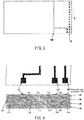
- FIG. 7 is a perspective view schematically showing this state.
- the forgoing first embodiment has described an example in which four circuit boards are laminated, but as an application of the present invention, it is also possible that, when a plurality of circuit boards are laminated, the circuit boards are bonded to each other while being classified into several groups, through-holes are formed in each group of laminated boards, then these groups of laminated boards are laid to overlap each other, and through-vias are formed. Furthermore, it is also conceivable that the present invention is applied to each group of laminated boards to subject the group of laminated boards to processing until the formation of through-vias, and then the groups of laminated boards are further laminated.
- Laminated circuit boards 500, 600, and 700 to which the present invention was applied are formed in advance.
- the laminated circuit board 500 is obtained by laminating two circuit boards
- the laminated circuit board 600 is obtained by laminating four circuit boards
- the laminated circuit board 700 is obtained by laminating five circuit boards.
- the laminated board 500 has through-vias 501, 502, 503, 504, 505, 506, 507, and 508,
- the laminated board 600 has through-vias 601, 602, 603, 604, 605, 606, 607, 608, 609, and 610
- the laminated board 700 has through-vias 701, 702, 703, 704, 705, 706, 707, 708, 709, and 710.
- a laminated integrated device 800 is obtained by laminating these three laminated boards.
- the present embodiment relates to an integration of illuminance sensor arrays, a temperature sensor, and an organic semiconductor circuit, but if these are formed on the same flexible board, the area of the integrated devices increases, and thus the yield ratio greatly decreases. In the experiment, the yield ratio never exceeded 20%. When the present invention was applied, it was observed that a yield ratio of about 80% could be achieved.
Landscapes
- Engineering & Computer Science (AREA)
- Microelectronics & Electronic Packaging (AREA)
- Manufacturing & Machinery (AREA)
- Production Of Multi-Layered Print Wiring Board (AREA)
- Combinations Of Printed Boards (AREA)
- Printing Elements For Providing Electric Connections Between Printed Circuits (AREA)
Applications Claiming Priority (2)
| Application Number | Priority Date | Filing Date | Title |
|---|---|---|---|
| JP2015027013 | 2015-02-13 | ||
| PCT/JP2016/055734 WO2016129705A1 (ja) | 2015-02-13 | 2016-02-12 | 積層回路基板の形成方法及びこれにより形成された積層回路基板 |
Publications (2)
| Publication Number | Publication Date |
|---|---|
| EP3258752A1 true EP3258752A1 (de) | 2017-12-20 |
| EP3258752A4 EP3258752A4 (de) | 2018-10-17 |
Family
ID=56614810
Family Applications (1)
| Application Number | Title | Priority Date | Filing Date |
|---|---|---|---|
| EP16749345.1A Pending EP3258752A4 (de) | 2015-02-13 | 2016-02-12 | Verfahren zur formung einer laminierten leiterplatte und unter verwendung davon laminierte leiterplatte |
Country Status (5)
| Country | Link |
|---|---|
| US (2) | US11122693B2 (de) |
| EP (1) | EP3258752A4 (de) |
| JP (1) | JP6489713B2 (de) |
| CN (1) | CN107211548B (de) |
| WO (1) | WO2016129705A1 (de) |
Cited By (1)
| Publication number | Priority date | Publication date | Assignee | Title |
|---|---|---|---|---|
| US11522234B2 (en) | 2017-09-06 | 2022-12-06 | Semiconductor Energy Laboratory Co., Ltd. | Semiconductor device, battery unit, and battery module |
Families Citing this family (3)
| Publication number | Priority date | Publication date | Assignee | Title |
|---|---|---|---|---|
| US10356902B2 (en) * | 2015-12-26 | 2019-07-16 | Intel Corporation | Board to board interconnect |
| KR102212009B1 (ko) * | 2019-04-08 | 2021-02-03 | 충남대학교 산학협력단 | 플렉서블 기판 기반의 하이브리드 집적회로 장치 및 그의 제조 방법 |
| US20230326823A1 (en) * | 2022-04-06 | 2023-10-12 | Infineon Technologies Ag | Temperature Sensor Arrangement in Semiconductor Module |
Family Cites Families (38)
| Publication number | Priority date | Publication date | Assignee | Title |
|---|---|---|---|---|
| JPH0369191A (ja) * | 1989-08-08 | 1991-03-25 | Nec Corp | 電子部品内蔵の多層プリント基板 |
| JP3198796B2 (ja) * | 1993-06-25 | 2001-08-13 | 富士電機株式会社 | モールドモジュール |
| JPH09331153A (ja) * | 1996-06-11 | 1997-12-22 | Toshiba Chem Corp | 多層フレキシブル配線板の製造方法 |
| US5729896A (en) * | 1996-10-31 | 1998-03-24 | International Business Machines Corporation | Method for attaching a flip chip on flexible circuit carrier using chip with metallic cap on solder |
| JPH10326970A (ja) * | 1997-05-23 | 1998-12-08 | Toshiba Corp | フレキシブルプリント配線板及びその製造方法 |
| US6159586A (en) * | 1997-09-25 | 2000-12-12 | Nitto Denko Corporation | Multilayer wiring substrate and method for producing the same |
| JP4547728B2 (ja) | 1999-03-29 | 2010-09-22 | ソニー株式会社 | 半導体装置及びその製造方法 |
| JP2001077501A (ja) * | 1999-09-03 | 2001-03-23 | Seiko Epson Corp | フレキシブル配線基板、電気光学装置および電子機器 |
| US6815709B2 (en) * | 2001-05-23 | 2004-11-09 | International Business Machines Corporation | Structure having flush circuitry features and method of making |
| KR100491179B1 (ko) | 2001-11-21 | 2005-05-24 | 마츠시타 덴끼 산교 가부시키가이샤 | 박형 회로기판 및 박형 회로기판의 제조방법 |
| JP4079626B2 (ja) * | 2001-11-21 | 2008-04-23 | 松下電器産業株式会社 | 薄型回路基板 |
| US7033959B2 (en) | 2002-05-31 | 2006-04-25 | Nokia Corporation | Method for manufacturing organic semiconductor systems |
| WO2004016054A1 (ja) * | 2002-08-07 | 2004-02-19 | Denso Corporation | 配線基板および配線基板の接続構造 |
| JP2005038951A (ja) * | 2003-07-17 | 2005-02-10 | Sumitomo Bakelite Co Ltd | 回路基板、多層基板、回路基板の製造方法および多層基板の製造方法 |
| JP2005116868A (ja) * | 2003-10-09 | 2005-04-28 | Nitto Denko Corp | 多層配線回路基板の製造方法 |
| US20050121225A1 (en) * | 2003-12-03 | 2005-06-09 | Phoenix Precision Technology Corporation | Multi-layer circuit board and method for fabricating the same |
| US6930240B1 (en) * | 2004-03-18 | 2005-08-16 | Agilent Technologies, Inc. | Flex-circuit shielded connection |
| US7543376B2 (en) * | 2004-10-20 | 2009-06-09 | Panasonic Corporation | Manufacturing method of flexible printed wiring board |
| JP2006179589A (ja) * | 2004-12-21 | 2006-07-06 | Matsushita Electric Ind Co Ltd | 多層フレキシブル配線基板、その製造方法および多層フレキシブル配線の回路基板との接続方法 |
| JP4955970B2 (ja) * | 2005-09-20 | 2012-06-20 | 住友電気工業株式会社 | フレキシブルプリント配線板およびその製造方法 |
| JP2007173477A (ja) * | 2005-12-21 | 2007-07-05 | Sumitomo Electric Ind Ltd | フレキシブルプリント配線板 |
| JP2007335675A (ja) * | 2006-06-15 | 2007-12-27 | Fuji Electric Systems Co Ltd | 電源装置および電源装置の製造方法 |
| US20080017305A1 (en) * | 2006-07-21 | 2008-01-24 | Teamchem Company | Method for fabricating multi-layered printed circuit board without via holes |
| JP2008071902A (ja) * | 2006-09-13 | 2008-03-27 | Fujifilm Corp | 配線方法 |
| JP4653726B2 (ja) * | 2006-12-08 | 2011-03-16 | 住友電気工業株式会社 | フレキシブル配線板の接続構造およびフレキシブル配線板の接続方法 |
| JP2008153441A (ja) * | 2006-12-18 | 2008-07-03 | Koa Corp | 配線基板およびその製造方法 |
| KR101391807B1 (ko) * | 2007-01-03 | 2014-05-08 | 삼성디스플레이 주식회사 | 잉크젯 프린팅과 나노 임프린팅을 이용한 패턴 형성 방법 |
| JP2008258357A (ja) * | 2007-04-04 | 2008-10-23 | Fujikura Ltd | リジッドフレキ基板とその製造方法 |
| CN101282637A (zh) * | 2007-04-06 | 2008-10-08 | 富葵精密组件(深圳)有限公司 | 柔性电路板表面贴装承载装置 |
| JP2008294337A (ja) * | 2007-05-28 | 2008-12-04 | Japan Electronic Materials Corp | セラミック基板 |
| KR101238178B1 (ko) * | 2007-10-29 | 2013-02-28 | 히타치가세이가부시끼가이샤 | 회로 접속 재료, 접속 구조체 및 그의 제조 방법 |
| JP5184335B2 (ja) * | 2008-12-26 | 2013-04-17 | 株式会社フジクラ | プリント配線板およびその製造方法、プリント配線板の接続方法 |
| WO2012061008A1 (en) * | 2010-10-25 | 2012-05-10 | Hsio Technologies, Llc | High performance electrical circuit structure |
| JP5455034B2 (ja) * | 2009-12-09 | 2014-03-26 | ホシデン株式会社 | フレキシブル配線基板 |
| TW201130405A (en) * | 2010-02-23 | 2011-09-01 | Ibiden Co Ltd | Flex-rigid wiring board and method for manufacturing the same |
| US20140120401A1 (en) * | 2012-10-30 | 2014-05-01 | Samsung Sdi Co., Ltd. | Connecting structure between circuit boards and battery pack having the same |
| JP2014212181A (ja) * | 2013-04-18 | 2014-11-13 | 船井電機株式会社 | 多層基板 |
| TWI667865B (zh) * | 2014-05-07 | 2019-08-01 | 易鼎股份有限公司 | Flexible circuit board line lap structure |
-
2016
- 2016-02-12 EP EP16749345.1A patent/EP3258752A4/de active Pending
- 2016-02-12 JP JP2016574880A patent/JP6489713B2/ja active Active
- 2016-02-12 CN CN201680008786.9A patent/CN107211548B/zh active Active
- 2016-02-12 WO PCT/JP2016/055734 patent/WO2016129705A1/ja not_active Ceased
-
2017
- 2017-08-14 US US15/676,472 patent/US11122693B2/en active Active
-
2019
- 2019-06-24 US US16/450,459 patent/US11985768B2/en active Active
Cited By (1)
| Publication number | Priority date | Publication date | Assignee | Title |
|---|---|---|---|---|
| US11522234B2 (en) | 2017-09-06 | 2022-12-06 | Semiconductor Energy Laboratory Co., Ltd. | Semiconductor device, battery unit, and battery module |
Also Published As
| Publication number | Publication date |
|---|---|
| EP3258752A4 (de) | 2018-10-17 |
| JP6489713B2 (ja) | 2019-03-27 |
| US11985768B2 (en) | 2024-05-14 |
| CN107211548A (zh) | 2017-09-26 |
| US20190313535A1 (en) | 2019-10-10 |
| JPWO2016129705A1 (ja) | 2018-01-11 |
| US20170374746A1 (en) | 2017-12-28 |
| WO2016129705A1 (ja) | 2016-08-18 |
| US11122693B2 (en) | 2021-09-14 |
| CN107211548B (zh) | 2021-10-29 |
Similar Documents
| Publication | Publication Date | Title |
|---|---|---|
| US11985768B2 (en) | Laminated circuit board | |
| CN105376936B (zh) | 具有集成的功率电子电路系统和逻辑电路系统的模块 | |
| EP1956878A3 (de) | Verfahren zur Herstellung einer mehrschichtigen Leiterplatte | |
| CN106158814B (zh) | 具有包埋无源组件的电路板和其制造方法 | |
| US20170179102A1 (en) | System in package | |
| US9589942B2 (en) | Package structure and manufacturing method thereof | |
| US20170094797A1 (en) | Printed circuit board and method for manufacturing the same | |
| EP1926136A3 (de) | Elektronisches Bauelement und Herstellungsverfahren dafür | |
| EP2423948A3 (de) | Seitliche Verbindung für einen Dünnfilmwiderstand ohne Kontaktlöcher und Herstellungsverfahren dafür | |
| WO2009037939A1 (ja) | プリント配線板及びその製造方法 | |
| EP1739747A3 (de) | Halbleiterchip und Verfahren zur Herstellung | |
| JP2011071315A5 (de) | ||
| KR101405328B1 (ko) | 연성 회로 기판 | |
| JP2018133572A (ja) | 多層配線基板およびこれを備えるプローブカード | |
| WO2008111408A1 (ja) | 多層配線基板及びその製造方法 | |
| TWI677271B (zh) | 線路基板及其製作方法 | |
| CN107454761B (zh) | 高密度增层多层板的制造方法 | |
| EP2654390A2 (de) | Struktur einer Gitterlücke einer elektrischen Leiterplatte | |
| KR20160110588A (ko) | 반도체 장치 및 그 제조 방법 | |
| US10453787B2 (en) | Method and apparatus for forming multi-layered vias in sequentially fabricated circuits | |
| TW201530728A (zh) | 具有嵌設元件的積體電路封裝系統及製造該積體電路封裝系統的方法 | |
| KR20110113980A (ko) | 필름을 포함한 다층 인쇄회로기판 및 그 제조 방법 | |
| WO2014195806A3 (en) | Methods and systems for insertion of spare wiring structures for improved engineering change orders | |
| US9578747B2 (en) | Structure of via hole of electrical circuit board | |
| CN110896590A (zh) | 线路基板及其制作方法 |
Legal Events
| Date | Code | Title | Description |
|---|---|---|---|
| STAA | Information on the status of an ep patent application or granted ep patent |
Free format text: STATUS: THE INTERNATIONAL PUBLICATION HAS BEEN MADE |
|
| PUAI | Public reference made under article 153(3) epc to a published international application that has entered the european phase |
Free format text: ORIGINAL CODE: 0009012 |
|
| STAA | Information on the status of an ep patent application or granted ep patent |
Free format text: STATUS: REQUEST FOR EXAMINATION WAS MADE |
|
| 17P | Request for examination filed |
Effective date: 20170913 |
|
| AK | Designated contracting states |
Kind code of ref document: A1 Designated state(s): AL AT BE BG CH CY CZ DE DK EE ES FI FR GB GR HR HU IE IS IT LI LT LU LV MC MK MT NL NO PL PT RO RS SE SI SK SM TR |
|
| AX | Request for extension of the european patent |
Extension state: BA ME |
|
| DAV | Request for validation of the european patent (deleted) | ||
| DAX | Request for extension of the european patent (deleted) | ||
| A4 | Supplementary search report drawn up and despatched |
Effective date: 20180917 |
|
| RIC1 | Information provided on ipc code assigned before grant |
Ipc: H05K 3/36 20060101ALI20180911BHEP Ipc: H05K 1/11 20060101ALI20180911BHEP Ipc: H05K 3/46 20060101AFI20180911BHEP Ipc: H05K 1/14 20060101ALI20180911BHEP Ipc: H05K 3/40 20060101ALI20180911BHEP |
|
| RAP3 | Party data changed (applicant data changed or rights of an application transferred) |
Owner name: PI-CRYSTAL INCORPORATION |
|
| STAA | Information on the status of an ep patent application or granted ep patent |
Free format text: STATUS: EXAMINATION IS IN PROGRESS |
|
| 17Q | First examination report despatched |
Effective date: 20210415 |
|
| GRAP | Despatch of communication of intention to grant a patent |
Free format text: ORIGINAL CODE: EPIDOSNIGR1 |
|
| STAA | Information on the status of an ep patent application or granted ep patent |
Free format text: STATUS: GRANT OF PATENT IS INTENDED |