EP2996247B1 - Démodulation de signaux modulés on-off-key dans des systèmes d'isolation de signaux - Google Patents
Démodulation de signaux modulés on-off-key dans des systèmes d'isolation de signaux Download PDFInfo
- Publication number
- EP2996247B1 EP2996247B1 EP15183914.9A EP15183914A EP2996247B1 EP 2996247 B1 EP2996247 B1 EP 2996247B1 EP 15183914 A EP15183914 A EP 15183914A EP 2996247 B1 EP2996247 B1 EP 2996247B1
- Authority
- EP
- European Patent Office
- Prior art keywords
- current
- transistors
- transistor
- signal
- output
- Prior art date
- Legal status (The legal status is an assumption and is not a legal conclusion. Google has not performed a legal analysis and makes no representation as to the accuracy of the status listed.)
- Active
Links
- 230000000295 complement effect Effects 0.000 claims description 4
- 238000002955 isolation Methods 0.000 description 11
- 238000000034 method Methods 0.000 description 6
- 230000004044 response Effects 0.000 description 6
- 230000004888 barrier function Effects 0.000 description 5
- 230000008569 process Effects 0.000 description 4
- 230000000694 effects Effects 0.000 description 3
- 230000000737 periodic effect Effects 0.000 description 3
- 230000007704 transition Effects 0.000 description 3
- 230000004913 activation Effects 0.000 description 2
- 238000004891 communication Methods 0.000 description 2
- 238000005516 engineering process Methods 0.000 description 2
- 210000002569 neuron Anatomy 0.000 description 2
- 238000004513 sizing Methods 0.000 description 2
- 230000005355 Hall effect Effects 0.000 description 1
- 230000009471 action Effects 0.000 description 1
- 230000005540 biological transmission Effects 0.000 description 1
- 239000003990 capacitor Substances 0.000 description 1
- 230000003750 conditioning effect Effects 0.000 description 1
- 230000005669 field effect Effects 0.000 description 1
- 230000036039 immunity Effects 0.000 description 1
- 230000003287 optical effect Effects 0.000 description 1
- 230000005693 optoelectronics Effects 0.000 description 1
- 230000004043 responsiveness Effects 0.000 description 1
- 230000035945 sensitivity Effects 0.000 description 1
- 230000011664 signaling Effects 0.000 description 1
- 230000002123 temporal effect Effects 0.000 description 1
Images


Classifications
-
- H—ELECTRICITY
- H04—ELECTRIC COMMUNICATION TECHNIQUE
- H04L—TRANSMISSION OF DIGITAL INFORMATION, e.g. TELEGRAPHIC COMMUNICATION
- H04L27/00—Modulated-carrier systems
- H04L27/02—Amplitude-modulated carrier systems, e.g. using on-off keying; Single sideband or vestigial sideband modulation
- H04L27/06—Demodulator circuits; Receiver circuits
-
- H—ELECTRICITY
- H03—ELECTRONIC CIRCUITRY
- H03K—PULSE TECHNIQUE
- H03K5/00—Manipulating of pulses not covered by one of the other main groups of this subclass
- H03K5/22—Circuits having more than one input and one output for comparing pulses or pulse trains with each other according to input signal characteristics, e.g. slope, integral
- H03K5/24—Circuits having more than one input and one output for comparing pulses or pulse trains with each other according to input signal characteristics, e.g. slope, integral the characteristic being amplitude
- H03K5/2472—Circuits having more than one input and one output for comparing pulses or pulse trains with each other according to input signal characteristics, e.g. slope, integral the characteristic being amplitude using field effect transistors
- H03K5/2481—Circuits having more than one input and one output for comparing pulses or pulse trains with each other according to input signal characteristics, e.g. slope, integral the characteristic being amplitude using field effect transistors with at least one differential stage
-
- H—ELECTRICITY
- H04—ELECTRIC COMMUNICATION TECHNIQUE
- H04L—TRANSMISSION OF DIGITAL INFORMATION, e.g. TELEGRAPHIC COMMUNICATION
- H04L25/00—Baseband systems
- H04L25/02—Details ; arrangements for supplying electrical power along data transmission lines
- H04L25/08—Modifications for reducing interference; Modifications for reducing effects due to line faults ; Receiver end arrangements for detecting or overcoming line faults
Definitions
- the present invention relates to signal isolators and, particularly, signal isolators that operate according to an on-off keyed signal protocol.
- Isolators are devices that exchange data signals between two galvanically isolated circuit systems.
- the two circuit systems each operate in different voltage domains, which may include different supply voltages and different ground references.
- Isolation devices may provide data exchange across an isolation barrier, which maintains the galvanic isolation.
- Typical isolation devices include micro-transformers, capacitors, magneto-resistors/giant magneto-resistors and opto-electronic devices.
- On-off keying is a signaling protocol that identifies a digital state of input data based on the type of signal that is transmitted through the isolation barrier.
- a first digital data state (say, a digital "1”) might be signaled by transmitting a periodic signal across the isolation barrier.
- a second digital data state (a digital "0") might be signaled by transmitting no signal across the isolation barrier.
- a receiver circuit would detect the presence or absence of the periodic signal and decode a digital output signal therefrom.
- OOK-based signal isolators typically have inefficient designs.
- isolator receivers may include a multiplier (or mixer) and an integrator as an energy detector for OOK demodulation.
- a mixer however, has a limited ability to handle common mode noise. Integrators typically are very slow for applications that require high data rate transmission across the isolation barrier.
- BHAT N ET AL "Asymmetric Cross-Coupled Differential Pair Configuration to Realize Neuron Activation Function and Its Derivative", IEEE TRANSACTIONS ON CIRCUITS AND SYSTEMS II: ANALOG AND DIGITALSIGNAL PROCESSING, INSTITUTE OF ELECTRICAL AND ELECTRONICS ENGINEERS INC, 345 EAST 47 STREET, NEW YORK, N.Y. 10017, USA, (20050101), vol. 52, no. 1, January 2005 , discloses: a circuit technique to generate the sigmoid neuron activation function (NAF) and its derivative (DNAF). The circuit makes use of transistor asymmetry in cross-coupled differential pair to obtain the derivative. The asymmetry is introduced through external control signal, as and when required. This results in the efficient utilization of the hardware by realizing NAF and DNAF using the same building blocks.
- Embodiments of the present invention provide a receiver system for an on-off key isolator system.
- the system may include a receiver that generates an intermediate current signal based on an OOK input signal.
- the intermediate current may be provided at a first current level when the input signal has a first OOK state and a second current level when the input signal has a second OOK state.
- the system also may include an output driver to generate a voltage representation of the intermediate current signal. Performing signal processing in a current domain permits fast transitions between OOK states.
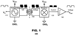
- FIG. 1 illustrates an isolator system 100 according to an embodiment of the present invention.
- the system 100 may include a transmitter 110, an isolator 120, a receiver 130 and an output driver 140.
- the isolator 120 may span an isolation boundary 150, which galvanically isolates two voltage domains from each other.
- the transmitter 110 may belong to a first voltage domain, which possesses its own voltage and ground supplies (shown as V DD1 , GND 1 ).
- the receiver 130 and output driver 140 may belong to a second voltage domain, which possesses voltage and ground supplies (V DD2 , GND 2 ) separate from the supplies of the first voltage domain.
- the isolation boundary 150 may prevent communication of voltages from one domain to the other.
- the system 100 may be provided for communication of digital data from the first voltage domain to the second voltage domain by on-off keying ("OOK" for short).
- the transmitter 110 may receive an input signal that takes one of two binary voltage levels.
- the transmitter 110 may generate an output signal having a state that is determined from the state of the input signal. For example, if the input signal corresponds to a binary value of "1,” the transmitter 110 may generate a periodic signal as its output but, if the input signal corresponds to a binary value of "0,” the transmitter 110 may output an inert signal (no activity). This action of toggling between an active state and an inactive state based on the state of the input signal represents one example of an on-off keyed output.
- the isolator 120 may be provided as a micro-transformer (shown in FIG 1 ), capacitive isolators, magneto-resistive sensors, an optical signal isolator or as Hall effect devices.
- the isolator 120 may receive the output from the transmitter 110 in the first voltage domain and pass a received signal to the receiver 130 in the second voltage domain.
- the received signal is illustrated as a copy of the OOK output that the isolator 120 receives from the transmitter 110, the received signal may include perturbations (not illustrated) that are induced into the signal by the isolator 120, for example, shifts in voltage, distortions induced by the isolator's temporal response and noise effects.
- the received signal may be provided to the receiver 130 as a voltage.
- the receiver 130 and output driver 140 may form an OOK receiver system in aggregate.
- the receiver 130 may generate a current signal from the OOK signal supplied to it by the isolator 120.
- the output driver 140 may generate a voltage signal from the current signal supplied to it by the receiver 130.
- the receiver 130 and output driver 140 may exchange current domain signals to provide a low latency output in response to OOK signals provided by the isolator 120.
- FIG. 2 illustrates a receiver 200 according to an embodiment of the present invention, which may be employed as a receiver in the system of FIG. 1 .
- the receiver 200 may include a current source 210, two differential pair circuits 220, 230 and a pair of current mirrors 240, 250.
- the differential pair circuits 220, 230 each may include a pair of mismatched transistors 222, 224 for pair 220 and 232, 234 for pair 230.
- the transistors in each pair 220, 230 may be mismatched according to a predetermined sizing ratio, shown as N to 1.
- transistors 222 and 232 may be N times larger than their counterpart transistors 224 and 234.
- the transistors 222, 232 may pass N times more current than the counterpart transistors 224 and 234.
- the input signal V IN may be a differential signal represented by component signals V INN and V INP .
- Gates of transistors 222 and 234 may receive a first input voltage V INP and gates of the other transistors 224 and 232 may receive a second input voltage V INN .
- Sources of the transistors 222, 224 in the first differential pair 220 may be connected to a common node, which may be coupled to a transistor 244 within the current mirror 240.
- Sources of the transistors 232, 234 in the second differential pair 230 may be connected to a second node, which may be coupled to another transistor 246 within the current mirror 240.
- Drains of the unit-sized transistors 224, 234 of the two differential pairs 220, 230 may be connected together and connected to a first transistor 252 in the second current mirror 250. Drains of the N-sized transistors 222, 232 of the two differential pairs 220, 230 may be connected to voltage supplies V DD .
- the first current mirror 240 may include a plurality of transistors 242-248 whose gates are connected together.
- the first transistor 242 may be connected to the current source 210 at its drain.
- the first transistor 242 also may be configured in a diode-connected configuration.
- an amount of current that passes through the first transistor 242 (which is defined by the current source 210) defines the amount of current that passes through the remaining transistors 244-248 of the current mirror 240.
- the transistors 244-248 may be sized so that twice as much current passes through transistors 244 and 246 as passes through transistor 248 (shown as I B and 1 ⁇ 2I B , respectively).
- the second current mirror 250 may include a pair of transistors 252 and 254. As discussed, a first transistor 252 may be connected to the unit-sized transistors 224 and 234 of the differential pairs 220, 230. The second transistor 254 may be connected to the transistor 248 in the first current mirror 240. The first transistor 252 may be provided in a diode-connected configuration. Thus, the current that passes through transistor 252 defines an amount of current that passes through transistor 254.
- An output terminal I OUT of the receiver 200 may be provided at the connection between transistors 254 and 248.
- the transistors 254 and 248 perform a current comparison at the output terminal I OUT .
- the transistor 248 may sink an amount of current from the output terminal equal to 1 ⁇ 2I B .
- the transistor 254 may source an amount of current I SIG to the output terminal in an amount that is determined by the differential pairs 220, 230, which in turn is determined by the input signals V INP and V INN .
- I SIG # 1 ⁇ 2I B a residual current is either sourced to or sunk from the output terminal I OUT .
- the transistors are illustrated as MOSFET transistors and, specifically, transistors 222-224, 232-234 and 242-248 are illustrated as NMOS transistors and transistors 252-254 are illustrated as PMOS transistors.
- the principles of the present invention apply to transistors of other process technologies, such as BJT transistors and the like.
- process types may be inverted (e.g., PMOS transistors may be provided where NMOS transistors are illustrated and NMOS transistors may be provided where PMOS transistors are illustrated) with appropriate inversion of supply voltages.
- process types may be inverted (e.g., PMOS transistors may be provided where NMOS transistors are illustrated and NMOS transistors may be provided where PMOS transistors are illustrated) with appropriate inversion of supply voltages.
- Such variations are immaterial to the principles of the present invention unless mentioned herein.
- FIG. 3 illustrates exemplary input and output signals that may be processed by the receiver of FIG. 2 .
- the input signals V INP and V INN may toggle between two phases of operation according to the OOK signal structure of the system.
- the OOK signal In a first phase of operation, the OOK signal may be in an "OFF" state in which V INP and V INN are inactive signals.
- V INP and V INN each have voltages of 1 ⁇ 2V DD .
- the OOK signal may be in an "ON" state in which V INP and V INN are active signals.
- the V INP and V INN signals oscillate between V DD and ground, centered about 1 ⁇ 2V DD .
- V INP and V INN may not be full rail signals (e.g., transitioning fully to ground or to V DD ) owing to losses within the circuit system.
- the transistors 222, 224, 232, 234 of the differential pairs 220, 230 may become partially conductive.
- the transistors 222, 232 may source N times as much current to their respective transistors 244, 246 in the current mirror 240 than the transistors 224, 234 do.
- the current mirror transistors 244, 246 each govern current through the differential pairs 220, 230, limiting the total current through each pair 220, 230 to I B .
- transistors 224 and 234 each pass current in the amount of 1 N + 1 I B and the transistors 222, 232 each pass the remainder of the current N N + 1 I B .
- V INP and V INN may oscillate between V DD and ground. Conductivity of the transistors 222, 224, 232, 234 of the differential pairs 220, 230 may vary according to these signals.
- V INP When V INP is at its maximum level, for example, transistors 222 and 234 may be nearly fully conductive. At this same time, V INN will be at its minimum level, which may render transistors 224 and 232 minimally conductive. Thus, transistors 222 and 234 each may pass nearly all of the current (I B ) that their associated current mirror transistors 244 and 246 sink.
- the current passed by transistor 224 may be sourced by transistor 252 in the second current mirror.
- the second transistor 254 in the second current mirror 250 may generate a current I SIG at I B .
- transistors 232 and 224 may be nearly fully conductive.
- V INP will be at its minimum level, which may render transistors 222 and 234 minimally conductive.
- transistors 224 and 232 each may pass nearly all of the current (I B ) that their associated current mirror transistors 244 and 246 sink.
- the current passed by transistor 234 may be sourced by transistor 252 in the second current mirror.
- the second transistor 254 in the second current mirror 250 may generate a current I SIG at I B .
- the I SIG current may vary in response to the V INP and V INN input signals as shown in FIG. 3 .
- the I SIG current may be compared to the 1 ⁇ 2I B current that is sunk from the output terminal by the current mirror transistor 248.
- the receiver of FIG. 2 may generate an output current I OUT having the form illustrated in FIG. 3 .
- FIG. 4 illustrates a current comparator 400 according to an embodiment of the present invention.
- the comparator 400 may include an inverter 410, a pair of pulling transistors 420, 430, current sources 440 and 450 and one or more inverters 460.
- the inverter 410 may accept a current input I IN on an input terminal.
- the input current may be an output current I OUT generated by a receiver such as those described in FIGS. 1 , 2 , 6 and 8 of this disclosure.
- the input terminal I IN also may be connected to a first supply voltage V DD by a first transistor 420 and to a second supply voltage (shown as ground) by a second transistor 430. Gates of the transistors 420, 430 may be coupled to an output of the inverter 410. The transistors 420, 430 may provide a positive feedback control within the comparator 400 to pull an input signal in the direction of one of the supplies V DD or ground as the input current I IN drives the inverter's input in that direction.
- the inverter 410 may be connected to the supply voltages V DD and ground by respective current sources 440, 450.
- the current sources 440, 450 may limit responsiveness of the inverter 410 to transitions in the input current signal IIN, which helps to filter signal glitches and other transients that otherwise might by introduced by noise within the system.
- the inverter(s) 460 may buffer a voltage output provided by the inverter 410.
- the inverters 460 may include filters or other signal conditioning circuits (not shown) to filter transients from the inverter's output.
- a voltage V OUT output from the inverters 460 may be output from the isolator system as a digital output signal.
- FIG. 5 illustrates exemplary input and output signals that may be processed by the comparator 400 of FIG. 4 .
- the input current I IN is shown as the output current signal I OUT in FIG. 3 .
- the output signal generated from the input current I IN is shown as V OUT .
- FIG. 6 illustrates a receiver 600 according to another embodiment of the present invention.
- the receiver 600 may include a plurality of current sources 610, 612, 614, two differential pair circuits 620, 630 and a current mirror 640.
- the current sources 610 and 612 may supply currents to an associated differential pair circuit 620 or 630 at a first level I B .
- the current source 614 may source current to an output terminal I OUT at a level that is half the level of current sources 610 and 620 (e.g., 1 ⁇ 2I B ).
- the differential pair circuits 620, 630 each may include a pair of mismatched transistors 622, 624 for differential pair circuit 620 and 632, 634 for differential pair circuit 630.
- the transistors in each pair 620, 630 may be mismatched according to a predetermined sizing ratio, shown as N to 1.
- transistors 622 and 632 may be N times larger than their counterpart transistors 624 and 634.
- the transistors 622, 632 may pass N times more current than the counterpart transistors 624 and 634.
- the input signal V IN may be a differential signal represented by component signals V INN and V INP .
- Gates of transistors 622 and 634 may receive a first input voltage V INP and gates of the other transistors 624 and 632 may receive a second input voltage V INN .
- Sources of the transistors 622, 624 in the first differential pair circuit 620 may be connected to a common node, which may be coupled to current source 610.
- Sources of the transistors 632, 634 in the second differential pair 630 may be connected to a second node, which may be coupled to another current source 620.
- Drains of the unit-sized transistors 624, 634 of the two differential pair circuits 620, 630 may be connected together and connected to a first transistor 642 in the second current mirror 640. Drains of the N-sized transistors 622, 632 of the two differential pair circuits 620, 630 may be connected to a voltage supply (ground, in this case).
- the current mirror 640 may include a pair of transistors 642 and 644. As discussed, a first transistor 642 may be connected to the unit-sized transistors 624 and 634 of the differential pairs 620, 630. The second transistor 644 may be connected to the current source 614. The first transistor 642 may be provided in a diode-connected configuration. Thus, the current that passes through transistor 642 defines an amount of current that passes through transistor 644.
- An output terminal I OUT of the receiver 600 may be provided at the connection between transistors 644 and current source 614.
- the transistor 644 and current source 614 perform a current comparison at the output terminal I OUT .
- the current source 614 may source an amount of current to the output terminal equal to 1 ⁇ 2I B .
- the transistor 644 may sink an amount of current I SIG from the output terminal I OUT in an amount that is determined by the differential pair circuits 620, 630, which in turn is determined by the input signals V INP and V INN .
- I SIG # 1 ⁇ 2I B a residual current is either sourced to or sunk from the output terminal I OUT .
- the circuit of FIG. 6 may operate in accordance with the principles discussed above with respect to FIG. 3 .
- the transistors 622-624, 632-634 of the differential pairs 620, 630 are illustrated as PMOS transistors rather than NMOS transistors as illustrated in FIG. 2 and, therefore, the conductivity of the transistors will be inverted from that of the FIG. 2 circuit during the ON phase.
- the circuit of FIG. 6 may generate a signal current I SIG as illustrated in FIG. 3 , which may be compared to the current 1 ⁇ 2I B of the current source 614 to generate the I OUT signal, also illustrated in FIG. 3 .
- FIG. 7 illustrates an output driver 700 according to another embodiment of the present invention.
- the output driver 700 may include an inverter 710, a pair of pulling transistors 715, 720, a pair of gating transistors 725, 730, a pair of current sources 735, 740 and one or more output inverters 745.
- An input current signal I IN may be input to an input of the inverter 710.
- the pulling transistors 715, 720 may couple the input terminal I IN to respective high and low voltage supplies V DD and ground. Gates of the pulling transistors 715, 720 may be coupled to an output of the inverter 710.
- the gating transistors 725 and 730 and current sources 735, 740 may be provided in pairs.
- a first transistor-current source pair 725, 735 may provide a second circuit path between the input terminal I IN and the high voltage supply V DD in parallel to a circuit path provided by the first pulling transistor 715.
- a second transistor-current source pair 730, 740 may provide a circuit path between the input terminal I IN and the low voltage supply (ground) in parallel to a circuit path that is provided by the second pulling transistor 720.
- the gating transistors and pulling transistors may be provided as complementary device types. In the example illustrated in FIG. 7 , the first pulling transistor 715 is illustrated as an NMOS transistor and the first gating transistor 725 is illustrated as a PMOS transistor.
- the second pulling transistor 720 is illustrated as a PMOS transistor and the second gating transistor 730 is illustrated as an NMOS transistor.
- a buffer 755 may be provided in a circuit path from the inverter output chain to a gate of transistor 715.
- current sources 735, 740 are illustrated as ideal current sources, their operation may be gated by their associated transistors 725 and 730. Thus, current source 735 will not supply current when its associated transistor 725 is rendered non-conductive. Similarly, current source 740 will not drive current when its associated transistor 730 is non-conductive. Gates of the gating transistors 725, 730 may be coupled to a node after one of the inverters 745. The provision of current sources 735 and 740 adds a hysteresis effect to operation of the output driver 700 which reduces its sensitivity to noise and other short term transients in the input current I IN .
- the output driver 700 may include one or more output inverters 745.
- Two output inverters 745.1, 745.2 are illustrated in FIG. 7 although different implementations may include other numbers of inverters as may be desired. Increasing the number of inverters may increase the driver's resistance to transients in the input current signal but also may increase the latency of the driver's response to key changes in the input signal.
- an input current I IN may be presented to the inverter 710, in the form illustrated in FIG. 3 .
- the inverter 710 may generate an output voltage at one of two levels, V DD or ground.
- the inverter's output may be input to the transistors 715-730.
- the transistor 715 When the inverter's output is set to V DD , the transistor 715 may become conductive, which allows the input current to pass to V DD .
- the transistor 715 may be sized to weakly pull the input node to V DD as compared to pulls exerted by the inverter 710.
- the transistor 720 When the inverter's output is set to ground, the transistor 720 may become conductive, which allows the input current to pass to ground.
- the transistor 720 also may be sized to weakly pull the input node to ground as compared to pulls exerted by the inverter 710.
- FIG. 8 illustrates a receiver circuit 800 according to another embodiment of the present invention.
- the receiver 800 may include four differential pair circuits 810-840, several current mirrors 850-880, and a plurality of current sources 890-896.
- the differential pair circuits 810-840 each may include a pair of mismatched transistors, shown as having a ratio of N to 1.
- Two differential pair circuits 810, 820 may have transistors 812, 814, 822 and 824 of a first doping type (NMOS transistors, in the example illustrated in FIG. 8 ) and the other two differential circuits 830, 840 may have transistors 832, 834, 842, 844 of a complementary doping type (e.g., PMOS transistors, in this example).
- Tails of each of the differential pair circuits 810-840 may be connected to respective current sources 890-896.
- the current mirrors 850-880 may be arranged to sum currents that pass through the N-sized transistors 812, 822, 832 and 842 and those that pass through the unit-sized transistors 814, 824, 834, 844.
- Current mirror 850 may have a first leg, provided by transistor 852, that is coupled to the unit-sized transistors 814, 824 of differential pairs 810 and 820 and a second leg, provided by transistor 854 for an output current ISIG N .
- the transistor 852 may be provided in a diode-connected configuration. Thus, an amount of current passed by the unit-sized transistors 814, 824 of the two differential pairs may be output to the second leg of the current mirror, also shown as ISIG N .
- the current mirror 860 may have a first leg, provided by transistor 862, that is coupled to the unit-sized transistors 834, 844 of differential pairs 830 and 840 and also to the output leg of current mirror 850.
- a second leg of the current mirror 860, provided by transistor 864, may be coupled to the output terminal I OUT .
- the transistor 862 may be provided in a diode-connected configuration.
- the current mirror 860 may generate a current signal ISIG representing a sum between ISIG N and the current passed by the unit-sized transistors 834, 844 of the second pair of differential pair circuits 830, 840.
- current mirror 870 may have a first leg, provided by transistor 872, that is coupled to the N-sized transistors 832, 842 of differential pairs 830 and 840 and a second leg, provided by transistor 874 for an output current IREF P .
- the transistor 874 may be provided in a diode-connected configuration.
- an amount of current passed by the N-sized transistors 832, 842 of the differential pairs 830 and 840 may be output to the second leg of the current mirror, also shown as IREF P .
- the current mirror 880 may have a first leg, provided by transistor 862, that is coupled to the N-sized transistors 812, 824 of differential pairs 810 and 820 and also to the output leg of current mirror 870.
- a second leg of the current mirror 880, provided by transistor 884, may be coupled to the output terminal I OUT .
- the transistor 882 may be provided in a diode-connected configuration.
- the current mirror 880 may generate a current signal IREF representing a sum between IREF P and the current passed by the N-sized transistors 812, 822 of the second pair of differential pair circuits 810, 820.
- the transistors 882, 884 of current mirror 880 may be mismatched transistors with transistor 882 being larger than transistor 884 (shown as being M times larger). In such an embodiment, the transistor 882 would pass M times the current that transistor 884 passes. In other words, the current I REF would be to 1/M th the current that passes through the N-sized transistors 812, 822, 832 and 842 of the differential pair circuits 810, 820, 830 and 840.
- the output terminal I OUT of the receiver 800 may be provided at the connection between transistors 884 and 864.
- the current mirrors 860 and 880 may perform a current comparison at the output terminal I OUT .
- the transistor 864 may sink an amount of current I SIG from the output terminal I OUT based on the amount of current sunk by the unit-sized transistors 814, 824, 834, 844 of the differential pair circuits 810, 820, 830 and 840.
- the transistor 884 may source an amount of current IREF to the output terminal I OUT based on the amount of current sunk by the N-sized transistors 812, 822, 832 and 842 of the differential pair circuits 810, 820, 830 and 840.
- I REF #I SIG a residual amount of current either would be sourced output from the receiver 800 or sunk by the receiver 800 through the I OUT terminal.
- the input signals V INP and V INN may toggle between two phases of operation according to the OOK signal structure of the system.
- the OOK signal may be in an "OFF" state in which V INP and V INN are inactive signals.
- V INP and V INN each may have voltages of 1 ⁇ 2V DD which may render all transistors of the differential pair circuits 810, 820, 830 and 840 partially conductive.
- the OOK signal may be in an "ON" state in which V INP and V INN are active signals.
- the V INP and V INN signals may oscillate between V DD and ground, centered about 1 ⁇ 2V DD . Again, V INP and V INN may not be full rail signals owing to losses within the circuit system.
- Conductivity of the transistors in the differential pair circuits 810, 820, 830 and 840 may vary according to these signals.
- N and M may be tuned to suit individual application needs. They should be set so that the current comparison at the output terminal (I OUT ) generates a first detectable state when the OOK signal is in an "OFF" state and another state when the OOK signal is in an "ON” state. Typically, M will be larger than 2.
- FIG. 8 provides several advantages over the design shown in, for example, FIG. 2 .
- the receiver 800 will remain responsive to input signals at both extremes of an input voltage (V DD and ground).
- Transistors of each type may be non-responsive when a difference of voltages between their gates and their sources fail to overcome a V GS threshold inherent to those transistors.
- the gate voltage must exceed the source voltage by the V GS thresholds and, when such transistors connect their sources to ground, the transistors may not be responsive to an input voltage that differs from ground by less than the transistor's V GS threshold.
- the gate voltage must be less than the source voltage by the V GS threshold and, when such transistors connect their sources to V DD , the transistors may not be responsive to an input voltage that differs from V DD by less than the transistor's V GS threshold.
- the differential pairs of one doping type say, those having the PMOS transistors
- the differential pairs of the complementary doping type may continue operation.
- the design of FIG. 8 may provide for rail-to-rail operation.
- FIG. 8 may conserve resources as compared to the design of FIG. 2 .
- current that passes through the N-sized transistors was sourced to the supplies (V DD and ground)
- the currents that are used in both the N-sized transistors and the unit-sized transistors are used to drive their respective current mirrors.
- the FIG. 8 embodiment may provide for more efficient use of resources.
- the receivers of the foregoing embodiments may be used cooperatively with a transmitter 110 that operates in a separate voltage domain that is isolated from a voltage domain of the receiver by an isolation boundary 150.
- Exemplary transmitters are illustrated in a co-pending application, filed on even date herewith, entitled “Methods and Structures to Generate On/Off Keyed Carrier Signals for Signal Isolators,” s.n. 14/486,937 (attorney docket 13641/518001), the disclosure of which is incorporated herein by reference.
Landscapes
- Engineering & Computer Science (AREA)
- Computer Networks & Wireless Communication (AREA)
- Signal Processing (AREA)
- Physics & Mathematics (AREA)
- Nonlinear Science (AREA)
- Power Engineering (AREA)
- Logic Circuits (AREA)
- Amplifiers (AREA)
- Electronic Switches (AREA)
Claims (7)
- Système récepteur de touche Marche/Arrêt (« OOK »), comprenant :- un récepteur (130) qui, en réponse à un signal d'entrée OOK, génère un signal de courant intermédiaire sur la base du signal d'entrée, le signal intermédiaire Iout comprenant un premier niveau de courant quand le signal d'entrée a un premier état OOK et un second niveau de courant quand le signal d'entrée a un second état OOK, et- un premier pilote de sortie (140) pour générer une représentation de tension du signal de courant intermédiaire ; et,caractérisé en ce que le récepteur comprend :. deux paires (810, 820 ; 830, 840) de circuits à paire différentielle non associés ayant des entrées pour un signal d'entrée différentiel, le signal d'entrée différentiel étant le signal d'entrée OOK, chaque circuit à paire différentielle comprenant une paire de transistors dont l'un a une conductibilité plus faible que l'autre, dans lequel un type dispositif de transistors dans les deux premiers des circuits à paire différentielle (810, 820) sont complémentaires d'un type dispositif de transistors dans les deux autres des circuits à paire différentielle (830, 840),. un premier miroir de courant (860) ayant une paire de chemins de courant, un premier chemin de courant couplé aux transistors à plus faible conductibilité des quatre circuits à paire différentielle et un deuxième chemin de courant couplé à une borne de sortie du récepteur,. un second miroir de courant (880) ayant une paire de chemins de courant, un premier chemin de courant couplé aux transistors à plus grande conductibilité des quatre circuits à paire différentielle et un deuxième chemin de courant couplé à la borne de sortie du récepteur, et. des sources de courant (890, 892, 894, 896) couplées à chacun des circuits à paire différentielle.
- Système selon la revendication 1 comprenant en outre :- un troisième miroir de courant (850) ayant une paire de chemins de courant, un premier chemin de courant couplé aux transistors à plus faible conductibilité des deux premiers circuits à paire différentielle et un deuxième chemin de courant couplé au premier chemin de courant du premier miroir de courant ; et- un quatrième miroir de courant (870) ayant une paire de chemins de courant, un premier chemin de courant couplé aux transistors à plus grande conductibilité des deux autres circuits à paire différentielle et un deuxième chemin de courant couplé au premier chemin de courant du deuxième miroir de courant.
- Système selon l'une quelconque des revendications précédentes, dans lequel le pilote de sortie comprend un onduleur.
- Système selon la revendication 3, dans lequel le pilote de sortie comprend en outre un moyen pour appliquer un retour positif à une entre du pilote de sortie.
- Système selon la revendication 3 ou 4, dans lequel le pilote de sortie comprend une pluralité d'onduleurs en cascade.
- Système selon la revendication 3, 4 ou 5, dans lequel le pilote de sortie comprend un onduleur à courant limité.
- Système selon la revendication 3, 4, 5 ou 6, dans lequel le pilote de sortie comprend en outre un filtre couplé à la sortie de l'onduleur.
Applications Claiming Priority (1)
| Application Number | Priority Date | Filing Date | Title |
|---|---|---|---|
| US14/486,951 US10270630B2 (en) | 2014-09-15 | 2014-09-15 | Demodulation of on-off-key modulated signals in signal isolator systems |
Publications (3)
| Publication Number | Publication Date |
|---|---|
| EP2996247A2 EP2996247A2 (fr) | 2016-03-16 |
| EP2996247A3 EP2996247A3 (fr) | 2016-06-22 |
| EP2996247B1 true EP2996247B1 (fr) | 2018-04-25 |
Family
ID=54150239
Family Applications (1)
| Application Number | Title | Priority Date | Filing Date |
|---|---|---|---|
| EP15183914.9A Active EP2996247B1 (fr) | 2014-09-15 | 2015-09-04 | Démodulation de signaux modulés on-off-key dans des systèmes d'isolation de signaux |
Country Status (3)
| Country | Link |
|---|---|
| US (1) | US10270630B2 (fr) |
| EP (1) | EP2996247B1 (fr) |
| CN (1) | CN105429624B (fr) |
Families Citing this family (12)
| Publication number | Priority date | Publication date | Assignee | Title |
|---|---|---|---|---|
| US10536309B2 (en) * | 2014-09-15 | 2020-01-14 | Analog Devices, Inc. | Demodulation of on-off-key modulated signals in signal isolator systems |
| US10270630B2 (en) * | 2014-09-15 | 2019-04-23 | Analog Devices, Inc. | Demodulation of on-off-key modulated signals in signal isolator systems |
| CN110063006B (zh) | 2016-10-13 | 2021-12-03 | 亚德诺半导体无限责任公司 | 用于跨越隔离屏障传输功率的系统和方法 |
| DE102018204782A1 (de) | 2018-03-28 | 2019-10-02 | Robert Bosch Gmbh | Detektorschaltung und System zur galvanisch-getrennten Übertragung digitaler Signale |
| US11018660B2 (en) | 2018-09-07 | 2021-05-25 | Analog Devices Global Unlimited Company | Multi-mode feedback control through digital isolator |
| US11204635B2 (en) | 2019-09-23 | 2021-12-21 | International Business Machines Corporation | Droop detection using power supply sensitive delay |
| US11281249B2 (en) | 2019-09-23 | 2022-03-22 | International Business Machines Corporation | Voltage sensitive current circuit |
| US10833653B1 (en) | 2019-09-23 | 2020-11-10 | International Business Machines Corporation | Voltage sensitive delay |
| US11152920B2 (en) * | 2019-09-23 | 2021-10-19 | International Business Machines Corporation | Voltage starved passgate with IR drop |
| US11533027B2 (en) | 2019-10-18 | 2022-12-20 | Analog Devices, Inc. | Low power receiver circuit for isolated data communications |
| CN111817709B (zh) * | 2020-09-04 | 2020-12-15 | 上海川土微电子有限公司 | 一种基于Efficient-OOK的数字隔离器电路及数字隔离器 |
| TWI737529B (zh) * | 2020-10-30 | 2021-08-21 | 精拓科技股份有限公司 | 數位隔離器 |
Family Cites Families (321)
| Publication number | Priority date | Publication date | Assignee | Title |
|---|---|---|---|---|
| US3058078A (en) | 1956-02-21 | 1962-10-09 | Siegfried R Hoh | Low capacitance transformer |
| US3537022A (en) | 1968-01-10 | 1970-10-27 | Hewlett Packard Co | Signal translating circuit |
| JPS5119739B1 (fr) | 1970-11-06 | 1976-06-19 | ||
| US3714540A (en) | 1970-11-10 | 1973-01-30 | Oxy Metal Finishing Corp | Isolation and transforming circuit |
| US3808673A (en) | 1971-03-17 | 1974-05-07 | Monsanto Co | Opto-isolator devices and method for the fabrication thereof |
| US3798608A (en) | 1972-12-15 | 1974-03-19 | Johnson Service Co | Digital signal transmission apparatus |
| US4065713A (en) | 1974-09-13 | 1977-12-27 | Nixdorf Computer Ag | Voltage stabilizer |
| DE2529296A1 (de) | 1975-07-01 | 1977-01-20 | Ferranti Ltd | Impuls-transformator |
| US6420992B1 (en) | 1975-08-26 | 2002-07-16 | Martin R. Richmond | On board jammer |
| US4035710A (en) | 1975-10-20 | 1977-07-12 | International Business Machines Corporation | Pulse width modulated voltage regulator-converter/power converter having means for improving the static stability characteristics thereof |
| US4027152A (en) * | 1975-11-28 | 1977-05-31 | Hewlett-Packard Company | Apparatus and method for transmitting binary-coded information |
| US4024452A (en) | 1976-03-10 | 1977-05-17 | Bell Telephone Laboratories, Incorporated | Integrated solid state isolator circuit |
| DE2760152C2 (de) | 1977-02-18 | 1985-06-20 | Robert Bosch Gmbh, 7000 Stuttgart | Differenzverstärker |
| US4118603A (en) | 1977-05-31 | 1978-10-03 | Noramco, Inc. | DC signaling circuit for use in conjunction with isolation transformers |
| US4227045A (en) | 1978-06-28 | 1980-10-07 | Honeywell Inc. | Data processing protocol system |
| WO1981000658A1 (fr) | 1979-08-31 | 1981-03-05 | Electro Med Eng Pty Ltd | Affaiblisseur non-reciproque de donnees de lignes telephoniques |
| US4275404A (en) | 1979-10-05 | 1981-06-23 | Bell Telephone Laboratories, Incorporated | Monolithic opto-isolator |
| CH647109A5 (de) | 1980-03-19 | 1984-12-28 | Studer Willi Fa | Differentialstufe mit genauem exponentiellem zusammenhang zwischen dem kollektorstromverhaeltnis und der spannung zwischen den beiden basen. |
| US4321487A (en) | 1980-04-07 | 1982-03-23 | Reliance Electric Company | Common mode rejection coupler |
| US4352998A (en) | 1980-04-07 | 1982-10-05 | Reliance Electric Company | Common mode rejection coupler |
| US4302807A (en) | 1980-08-04 | 1981-11-24 | Burroughs Corporation | Controlled current base drive circuit |
| US4547961A (en) | 1980-11-14 | 1985-10-22 | Analog Devices, Incorporated | Method of manufacture of miniaturized transformer |
| US4443839A (en) | 1980-12-23 | 1984-04-17 | Tokyo Shibaura Denki Kabushiki Kaisha | Single ended, separately driven, resonant DC-DC converter |
| US4318170A (en) | 1981-01-12 | 1982-03-02 | Cabalfin Rolando V | Power inverter oscillator circuit |
| JPS5946148B2 (ja) | 1981-02-10 | 1984-11-10 | 横河電機株式会社 | 絶縁装置 |
| US4538136A (en) | 1981-03-30 | 1985-08-27 | Amtel Systems Corporation | Power line communication system utilizing a local oscillator |
| US4554462A (en) | 1982-03-16 | 1985-11-19 | Fanuc Limited | Non-polarized contactless relay |
| JPS58164338U (ja) | 1982-04-27 | 1983-11-01 | フアナツク株式会社 | 無接点リレ− |
| JPS58215833A (ja) | 1982-06-10 | 1983-12-15 | Yamatake Honeywell Co Ltd | 磁気信号伝送装置 |
| US4475149A (en) | 1982-09-13 | 1984-10-02 | Venus Scientific Inc. | Resonant current-driven power source |
| US4818855A (en) | 1985-01-11 | 1989-04-04 | Indala Corporation | Identification system |
| GB2173956B (en) | 1985-03-29 | 1989-01-05 | Plessey Co Plc | Improvements relating to electric transformers |
| US4712170A (en) | 1985-04-25 | 1987-12-08 | Power Modifications Incorporated | Power supply having tuned radio frequency circuit |
| US4660014A (en) | 1985-06-19 | 1987-04-21 | Jaycor | Electromagnetic pulse isolation transformer |
| US4864589A (en) | 1985-07-24 | 1989-09-05 | Nec Home Electronics Ltd. | Spread spectrum power line communications |
| US4703283A (en) | 1986-02-24 | 1987-10-27 | Howard Samuels | Isolation amplifier with T-type modulator |
| US4780795A (en) | 1986-04-28 | 1988-10-25 | Burr-Brown Corporation | Packages for hybrid integrated circuit high voltage isolation amplifiers and method of manufacture |
| US4835486A (en) | 1986-04-28 | 1989-05-30 | Burr-Brown Corporation | Isolation amplifier with precise timing of signals coupled across isolation barrier |
| US4748419A (en) | 1986-04-28 | 1988-05-31 | Burr-Brown Corporation | Isolation amplifier with precise timing of signals coupled across isolation barrier |
| US4785345A (en) | 1986-05-08 | 1988-11-15 | American Telephone And Telegraph Co., At&T Bell Labs. | Integrated transformer structure with primary winding in substrate |
| US4720667A (en) | 1986-06-20 | 1988-01-19 | Lee Fred C | Zero-current switching quasi-resonant converters operating in a full-wave mode |
| US4879505A (en) | 1986-12-23 | 1989-11-07 | Analog Devices, Inc. | Temperature and power supply compensation circuit for integrated circuits |
| US4899152A (en) | 1986-12-23 | 1990-02-06 | Analog Devices, Inc. | Method and apparatus for temperature compensating a digital to analog converter |
| US4825450A (en) | 1987-03-12 | 1989-04-25 | The Boeing Company | Binary data communication system |
| US4924210A (en) | 1987-03-17 | 1990-05-08 | Omron Tateisi Electronics Company | Method of controlling communication in an ID system |
| US4737851A (en) | 1987-04-24 | 1988-04-12 | Rca Corporation | On/off control circuitry for television |
| US4845466A (en) | 1987-08-17 | 1989-07-04 | Signetics Corporation | System for high speed digital transmission in repetitive noise environment |
| DE3731020A1 (de) | 1987-09-11 | 1989-03-30 | Siemens Ag | Schaltungsanordnung zur uebertragung von sendeimpulsen zwischen zwei galvanisch getrennten stromkreisen |
| DE3731644A1 (de) | 1987-09-19 | 1989-03-30 | Thomson Brandt Gmbh | Schaltungsanordnung fuer ein geregeltes schaltnetzteil |
| US4885582A (en) | 1987-09-28 | 1989-12-05 | The Grass Valley Group, Inc. | "Simple code" encoder/decoder |
| US4959631A (en) | 1987-09-29 | 1990-09-25 | Kabushiki Kaisha Toshiba | Planar inductor |
| JPH01116281A (ja) | 1987-10-29 | 1989-05-09 | Aisin Seiki Co Ltd | 点火装置 |
| US5327030A (en) | 1987-11-13 | 1994-07-05 | Analog Devices, Inc. | Decoder and monolithic integrated circuit incorporating same |
| US4859877A (en) | 1988-01-04 | 1989-08-22 | Gte Laboratories Incorporated | Bidirectional digital signal transmission system |
| US4817865A (en) | 1988-03-17 | 1989-04-04 | Racal Data Communications Inc. | Ventilation system for modular electronic housing |
| US5041780A (en) | 1988-09-13 | 1991-08-20 | California Institute Of Technology | Integrable current sensors |
| CA1331214C (fr) | 1989-01-05 | 1994-08-02 | Kun-Ming Lee | Circuit de commande d'interface a dispositif actif de charge et de decharge |
| US4937468A (en) | 1989-01-09 | 1990-06-26 | Sundstrand Corporation | Isolation circuit for pulse waveforms |
| US4920474A (en) | 1989-03-23 | 1990-04-24 | North American Philips Corporation | High frequency high voltage power supply with controlled output power |
| JPH0377360A (ja) | 1989-08-18 | 1991-04-02 | Mitsubishi Electric Corp | 半導体装置 |
| US5057968A (en) | 1989-10-16 | 1991-10-15 | Lockheed Corporation | Cooling system for electronic modules |
| US5396394A (en) | 1990-02-06 | 1995-03-07 | International Business Machines Corp. | ISDN device line protection circuit |
| US5136455A (en) | 1990-03-16 | 1992-08-04 | Esp Electronic Systems Protection, Inc. | Electromagnetic interference suppression device |
| FR2662320B1 (fr) | 1990-05-18 | 1994-05-13 | Cemagref | Dispositif de liaison sans contact pour relier des troncons de bus serie. |
| DE69121043D1 (de) | 1990-10-18 | 1996-08-29 | Valor Electronics Inc | Nicht-gekoppelte integrierte magnetische Struktur |
| JPH04172711A (ja) | 1990-11-06 | 1992-06-19 | Mitsubishi Electric Corp | 半導体遅延回路 |
| US5128729A (en) | 1990-11-13 | 1992-07-07 | Motorola, Inc. | Complex opto-isolator with improved stand-off voltage stability |
| GB2252208B (en) | 1991-01-24 | 1995-05-03 | Burr Brown Corp | Hybrid integrated circuit planar transformer |
| US5102040A (en) | 1991-03-28 | 1992-04-07 | At&T Bell Laboratories | Method and apparatus for fan control to achieve enhanced cooling |
| US5204551A (en) | 1991-07-01 | 1993-04-20 | Motorola, Inc. | Method and apparatus for high power pulse modulation |
| KR960003163B1 (ko) * | 1991-07-15 | 1996-03-05 | 삼성전자주식회사 | 문자 정보 보상 장치 |
| FR2679670B1 (fr) | 1991-07-23 | 1993-10-29 | Dan Serbanescu | Systeme de communication bilaterale sans contacts pour les cartes de credit a microprocesseur. |
| US5450305A (en) | 1991-08-12 | 1995-09-12 | Auckland Uniservices Limited | Resonant power supplies |
| US5142432A (en) | 1991-10-21 | 1992-08-25 | General Motors Corporation | Fault detection apparatus for a transformer isolated transistor drive circuit for a power device |
| US5260967A (en) | 1992-01-13 | 1993-11-09 | Interdigital Technology Corporation | CDMA/TDMA spread-spectrum communications system and method |
| US5430641A (en) | 1992-04-27 | 1995-07-04 | Dell Usa, L.P. | Synchronously switching inverter and regulator |
| JP3141562B2 (ja) | 1992-05-27 | 2001-03-05 | 富士電機株式会社 | 薄膜トランス装置 |
| US5369666A (en) | 1992-06-09 | 1994-11-29 | Rockwell International Corporation | Modem with digital isolation |
| US5270882A (en) | 1992-07-15 | 1993-12-14 | International Business Machines Corporation | Low-voltage, low-power amplifier for magnetoresistive sensor |
| US5588021A (en) | 1992-09-25 | 1996-12-24 | Light & Sound Design Limited | Repeater for use in a control network |
| US5300896A (en) | 1992-10-16 | 1994-04-05 | Suesserman Michael F | Bootstrapped, AC-coupled differential amplifier |
| US5329225A (en) | 1992-11-02 | 1994-07-12 | General Electric Co. | Thin film superconductor inductor with shield for high frequency resonant circuit |
| US5444600A (en) | 1992-12-03 | 1995-08-22 | Linear Technology Corporation | Lead frame capacitor and capacitively-coupled isolator circuit using the same |
| US5334882A (en) | 1992-12-14 | 1994-08-02 | National Semiconductor | Driver for backplane transceiver logic bus |
| US5384808A (en) | 1992-12-31 | 1995-01-24 | Apple Computer, Inc. | Method and apparatus for transmitting NRZ data signals across an isolation barrier disposed in an interface between adjacent devices on a bus |
| WO1994017558A1 (fr) | 1993-01-29 | 1994-08-04 | The Regents Of The University Of California | Composant monolithique passif |
| US5325355A (en) * | 1993-03-19 | 1994-06-28 | Apple Computer, Inc. | Method and apparatus for implementing a common mode level shift in a bus transceiver incorporating a high speed binary data transfer mode with a ternary control transfer mode |
| US5469098A (en) | 1993-03-29 | 1995-11-21 | Exide Electronics Corporation | Isolated gate drive |
| US5339061A (en) | 1993-06-01 | 1994-08-16 | Michael Ebert | Iron-free transformer |
| CN1050242C (zh) | 1993-06-14 | 2000-03-08 | Vlt公司 | 电源变换装置、电源变换器控制装置及其制造电源变换器的方法 |
| US5568516A (en) | 1993-07-02 | 1996-10-22 | Phonic Ear Incorporated | Very low power cordless headset system |
| US5615229A (en) | 1993-07-02 | 1997-03-25 | Phonic Ear, Incorporated | Short range inductively coupled communication system employing time variant modulation |
| US5533054A (en) | 1993-07-09 | 1996-07-02 | Technitrol, Inc. | Multi-level data transmitter |
| AU6669194A (en) * | 1993-08-10 | 1995-02-28 | Microunity Systems Engineering, Inc. | Bicmos current mode driver and receiver |
| JPH07115768A (ja) | 1993-10-14 | 1995-05-02 | Japan Storage Battery Co Ltd | 共振形コンバータ |
| US5631920A (en) | 1993-11-29 | 1997-05-20 | Lexmark International, Inc. | Spread spectrum clock generator |
| US5488627A (en) | 1993-11-29 | 1996-01-30 | Lexmark International, Inc. | Spread spectrum clock generator and associated method |
| US5475579A (en) | 1993-12-20 | 1995-12-12 | At&T Corp. | Pulse width modulator for switching power supply |
| EP0742906B1 (fr) | 1994-01-31 | 1998-09-23 | Fraunhofer-Gesellschaft zur Förderung der angewandten Forschung e.V. | Utilisation d'un dispositif a bobines miniaturise, fabrique en technologie planaire, pour la detection de matieres ferromagnetiques |
| US5467607A (en) | 1994-02-22 | 1995-11-21 | At&T Corp. | Air conditioning control system |
| JP3213156B2 (ja) | 1994-03-15 | 2001-10-02 | 富士通株式会社 | 電子機器 |
| US5636110A (en) | 1994-04-26 | 1997-06-03 | Comarco Wireless Technologies, Inc. | Small form factor power supply |
| KR0165289B1 (ko) * | 1994-06-09 | 1999-03-20 | 김광호 | 멀티 텔레비젼 방송신호 수신장치 및 그 제어방법 |
| US6000128A (en) | 1994-06-21 | 1999-12-14 | Sumitomo Special Metals Co., Ltd. | Process of producing a multi-layered printed-coil substrate |
| EP0774187A1 (fr) | 1994-08-03 | 1997-05-21 | Madge Networks Limited | Isolateur d'interference electromagnetique |
| GB2292856B (en) * | 1994-08-31 | 1999-04-28 | Texas Instruments Ltd | Bus driver |
| GB9421402D0 (en) | 1994-10-21 | 1994-12-07 | Plessey Semiconductors Ltd | Power switch driver |
| US5701037A (en) | 1994-11-15 | 1997-12-23 | Siemens Aktiengesellschaft | Arrangement for inductive signal transmission between the chip layers of a vertically integrated circuit |
| US5539598A (en) | 1994-12-08 | 1996-07-23 | International Business Machines Corporation | Electrostatic protection for a shielded MR sensor |
| US5721506A (en) | 1994-12-14 | 1998-02-24 | Micron Technology, Inc. | Efficient Vccp supply with regulation for voltage control |
| JP3487461B2 (ja) | 1994-12-17 | 2004-01-19 | ソニー株式会社 | 変成器及び増幅器 |
| US5596466A (en) | 1995-01-13 | 1997-01-21 | Ixys Corporation | Intelligent, isolated half-bridge power module |
| US5913817A (en) | 1995-04-05 | 1999-06-22 | Karl Storz Imaging | Electrical isolation of endoscopic video camera |
| US5716323A (en) | 1995-04-05 | 1998-02-10 | Karl Storz Imaging | Electrical isolation of endoscopic video camera |
| US5774350A (en) | 1995-04-07 | 1998-06-30 | Sgs-Thomson Microelectronics S.A. | Integrated low dissipation power controller |
| JPH0937558A (ja) | 1995-07-14 | 1997-02-07 | Yokogawa Electric Corp | インバータ装置 |
| SE509882C2 (sv) | 1995-11-10 | 1999-03-15 | Ericsson Telefon Ab L M | Mottagarkrets innefattande parallella ingångskretsar |
| US5786979A (en) | 1995-12-18 | 1998-07-28 | Douglass; Barry G. | High density inter-chip connections by electromagnetic coupling |
| US5990753A (en) | 1996-01-29 | 1999-11-23 | Stmicroelectronics, Inc. | Precision oscillator circuit having a controllable duty cycle and related methods |
| CN1183587C (zh) | 1996-04-08 | 2005-01-05 | 德克萨斯仪器股份有限公司 | 用于把两个集成电路直流上相互隔离的方法和设备 |
| US5801602A (en) | 1996-04-30 | 1998-09-01 | 3Com Corporation | Isolation and signal filter transformer |
| US5877667A (en) | 1996-08-01 | 1999-03-02 | Advanced Micro Devices, Inc. | On-chip transformers |
| US5831426A (en) | 1996-08-16 | 1998-11-03 | Nonvolatile Electronics, Incorporated | Magnetic current sensor |
| US5757338A (en) | 1996-08-21 | 1998-05-26 | Neomagic Corp. | EMI reduction for a flat-panel display controller using horizontal-line based spread spectrum |
| US5731954A (en) | 1996-08-22 | 1998-03-24 | Cheon; Kioan | Cooling system for computer |
| US5910780A (en) | 1996-11-13 | 1999-06-08 | Analog Devices, Inc. | Switched-transconductance multiplexer circuit with integrated T-switches |
| US5714938A (en) | 1996-11-19 | 1998-02-03 | Cae Electronics Ltd. | Temperature protection device for air cooled electronics housing |
| JPH10178398A (ja) | 1996-12-17 | 1998-06-30 | K D D Technol:Kk | 入出力間電位絶縁装置 |
| JPH10191654A (ja) | 1996-12-24 | 1998-07-21 | Harumi Suzuki | インバータ回路およびその回路を用いた照明装置 |
| US5781077A (en) | 1997-01-28 | 1998-07-14 | Burr-Brown Corporation | Reducing transformer interwinding capacitance |
| US5952849A (en) | 1997-02-21 | 1999-09-14 | Analog Devices, Inc. | Logic isolator with high transient immunity |
| US6385235B1 (en) | 1997-04-22 | 2002-05-07 | Silicon Laboratories, Inc. | Direct digital access arrangement circuitry and method for connecting to phone lines |
| US6359983B1 (en) | 1997-04-22 | 2002-03-19 | Silicon Laboratories, Inc. | Digital isolation system with data scrambling |
| DE19718420A1 (de) | 1997-04-30 | 1998-11-12 | Siemens Ag | Integrierte Datenübertragungsschaltung mit Potentialtrennung zwischen Ein- und Ausgangsschaltkreis |
| JP2002508916A (ja) | 1997-05-06 | 2002-03-19 | オークランド ユニサービシズ リミテッド | 拡大ギャップを横切る誘導電力伝達 |
| US6377646B1 (en) | 1997-07-21 | 2002-04-23 | Cypress Semiconductor Corp. | Spread spectrum at phase lock loop (PLL) feedback path |
| US5969590A (en) | 1997-08-05 | 1999-10-19 | Applied Micro Circuits Corporation | Integrated circuit transformer with inductor-substrate isolation |
| US6038276A (en) * | 1997-08-26 | 2000-03-14 | Dinh; Truong T. | Digital phase lock loop for non-continuous reference signal |
| US5831525A (en) | 1997-09-18 | 1998-11-03 | Harvey; James C. | Filtered air, temperature controlled removable computer cartridge devices |
| US6188494B1 (en) | 1997-10-17 | 2001-02-13 | Schweitzer Engineering Laboratories, Inc. | Fiber-optic transceiver for long distance data communications |
| US6873065B2 (en) | 1997-10-23 | 2005-03-29 | Analog Devices, Inc. | Non-optical signal isolator |
| US20030042571A1 (en) * | 1997-10-23 | 2003-03-06 | Baoxing Chen | Chip-scale coils and isolators based thereon |
| US6054780A (en) | 1997-10-23 | 2000-04-25 | Analog Devices, Inc. | Magnetically coupled signal isolator using a Faraday shielded MR or GMR receiving element |
| SE520906C2 (sv) | 1997-10-28 | 2003-09-09 | Ericsson Telefon Ab L M | Spänningsregulator med ett mycket lågt 'drop-out voltage' |
| US6389063B1 (en) | 1997-10-31 | 2002-05-14 | Hitachi, Ltd. | Signal transmission apparatus using an isolator, modem, and information processor |
| JPH11252580A (ja) * | 1997-10-31 | 1999-09-17 | Texas Instr Inc <Ti> | ビデオデコーダ及びこれに用いるカラー位相ロックループ |
| US5907481A (en) | 1997-10-31 | 1999-05-25 | Telefonaktiebolaget Lm Ericsson | Double ended isolated D.C.--D.C. converter |
| US5942937A (en) | 1997-11-19 | 1999-08-24 | Advanced Micro Devices, Inc. | Signal detection circuit using a plurality of delay stages with edge detection logic |
| JP3247328B2 (ja) | 1997-12-09 | 2002-01-15 | 浩 坂本 | 非接触電力伝達装置 |
| US5900683A (en) | 1997-12-23 | 1999-05-04 | Ford Global Technologies, Inc. | Isolated gate driver for power switching device and method for carrying out same |
| US6025705A (en) | 1997-12-24 | 2000-02-15 | Intel Corporation | DC-to-DC converter |
| KR19990072936A (ko) | 1998-02-27 | 1999-09-27 | 가나이 쓰도무 | 아이솔레이터및그것을사용하는모뎀장치 |
| US6300617B1 (en) | 1998-03-04 | 2001-10-09 | Nonvolatile Electronics, Incorporated | Magnetic digital signal coupler having selected/reversal directions of magnetization |
| US6215374B1 (en) | 1998-03-16 | 2001-04-10 | Broadband Innovations, Inc. | Magnetically coupled resonators for achieving low cost narrow band pass filters having high selectivity, low insertion loss and improved out-of-band rejection |
| US6559692B2 (en) | 1998-04-24 | 2003-05-06 | Cirrus Logic, Inc. | Output driver for a 10baset/100basetx ethernet physical layer line interface |
| US6016050A (en) | 1998-07-07 | 2000-01-18 | Analog Devices, Inc. | Start-up and bias circuit |
| EP0977406B1 (fr) | 1998-07-17 | 2009-09-23 | Endress + Hauser Wetzer GmbH + Co. KG | Circuit de transmission de signaux numériques avec séparation galvanique |
| US6069802A (en) | 1998-07-31 | 2000-05-30 | Priegnitz; Robert A. | Transformer isolated driver and isolated forward converter |
| US6127663A (en) | 1998-10-09 | 2000-10-03 | Ericsson Inc. | Electronics cabinet cooling system |
| US6087882A (en) | 1998-12-04 | 2000-07-11 | Analog Devices, Inc. | Ultra-low power magnetically coupled digital isolator using spin valve resistors |
| IT1313381B1 (it) | 1999-02-22 | 2002-07-23 | St Microelectronics Srl | Comparatore per alta frequenza con isteresi, con segnale di ingressodifferenziale a bassa dinamica, compatibile alle alimentazioni |
| DE19922129C1 (de) | 1999-05-12 | 2000-09-28 | Siemens Ag | Verfahren und Vorrichtung zur logischen Verknüpfung von Signalen auf magnetischer Basis |
| DE19922127C2 (de) | 1999-05-12 | 2002-05-29 | Siemens Ag | Integrierter Schaltkreis mit einem A/D- oder D/A-Wandler mit galvanischer Trennung |
| DE19922123A1 (de) | 1999-05-12 | 2000-11-23 | Siemens Ag | Kompakte Busschnittstelle mit integrierter Potentialtrennung |
| DE19922128C1 (de) | 1999-05-12 | 2001-01-25 | Siemens Ag | Integrierter Schaltkreis zur Erzeugung eines Ansteuersignals für einen Isolated Gate Bipolar Transistor (IGBT) |
| US6255863B1 (en) * | 1999-05-20 | 2001-07-03 | Matsushita Electric Industrial Co., Ltd. | Circuit and method for determining level of differential signal |
| US6826390B1 (en) * | 1999-07-14 | 2004-11-30 | Fujitsu Limited | Receiver, transceiver circuit, signal transmission method, and signal transmission system |
| US6833875B1 (en) * | 1999-09-02 | 2004-12-21 | Techwell, Inc. | Multi-standard video decoder |
| US6377313B1 (en) * | 1999-09-02 | 2002-04-23 | Techwell, Inc. | Sharpness enhancement circuit for video signals |
| US6573940B1 (en) * | 1999-09-02 | 2003-06-03 | Techwell, Inc | Sample rate converters for video signals |
| JP3705966B2 (ja) | 1999-09-07 | 2005-10-12 | 東光株式会社 | スイッチング電源回路 |
| US6728320B1 (en) | 1999-09-23 | 2004-04-27 | Texas Instruments Incorporated | Capacitive data and clock transmission between isolated ICs |
| US6262616B1 (en) | 1999-10-08 | 2001-07-17 | Cirrus Logic, Inc. | Open loop supply independent digital/logic delay circuit |
| US6396329B1 (en) | 1999-10-19 | 2002-05-28 | Rambus, Inc | Method and apparatus for receiving high speed signals with low latency |
| WO2001037323A2 (fr) | 1999-11-03 | 2001-05-25 | Hwu R Jennifer | Transformateur vertical |
| US6553057B1 (en) | 1999-11-09 | 2003-04-22 | Cypress Semiconductor Corp. | Circuit and method for linear control of a spread spectrum transition |
| US6738240B1 (en) | 1999-12-10 | 2004-05-18 | Micron Technology, Inc. | Microtransformer for system-on-chip power supply |
| US6208174B1 (en) * | 1999-12-14 | 2001-03-27 | Analog Devices, Inc. | High-speed comparator systems and methods with enhanced noise rejection |
| WO2001044913A1 (fr) | 1999-12-15 | 2001-06-21 | Hitachi, Ltd. | Dispositif d'interface et systeme de traitement de l'information |
| US6262600B1 (en) | 2000-02-14 | 2001-07-17 | Analog Devices, Inc. | Isolator for transmitting logic signals across an isolation barrier |
| EP1130752B1 (fr) | 2000-02-24 | 2005-05-11 | Matsushita Electric Works, Ltd. | Système de transmission de puissance électrique comprenant une fonction pour maintenir constante la tension de charge |
| DE60012299T2 (de) | 2000-03-20 | 2005-06-30 | Motorola, Inc., Schaumburg | Einstellbarer Taktgenerator mit spektraler Dispersion und Verfahren hierfür |
| TW508938B (en) | 2000-06-28 | 2002-11-01 | Agere Syst Guardian Corp | Inductive coupling for silicon data access arrangement |
| JP3493575B2 (ja) | 2000-07-28 | 2004-02-03 | Necエレクトロニクス株式会社 | 半導体装置、チャージポンプ回路およびpll回路 |
| US6449318B1 (en) * | 2000-08-28 | 2002-09-10 | Telenetwork, Inc. | Variable low frequency offset, differential, OOK, high-speed twisted pair communication |
| FI20002493A (fi) | 2000-11-14 | 2002-05-15 | Salcomp Oy | Teholähdejärjestely ja induktiivisesti kytketty akkulaturi, jossa on langattomasti kytketty ohjaus, ja menetelmä teholähdejärjestelyn ja induktiivisesti kytketyn akkulaturin ohjaamiseksi langattomasti |
| US6542385B1 (en) | 2000-11-22 | 2003-04-01 | Teradyne, Inc. | DUT power supply having improved switching DC-DC converter |
| US6304109B1 (en) | 2000-12-05 | 2001-10-16 | Analog Devices, Inc. | High gain CMOS amplifier |
| FR2818824B1 (fr) | 2000-12-21 | 2003-03-21 | St Microelectronics Sa | Commutateur integre a commande par transformateur rf |
| SE0004794L (sv) | 2000-12-22 | 2002-06-23 | Ericsson Telefon Ab L M | En flerskikts-symmetreringstransformatorstruktur |
| DE10100282B4 (de) | 2001-01-04 | 2005-10-13 | Infineon Technologies Ag | Elektrischer Transformator |
| US6344979B1 (en) | 2001-02-09 | 2002-02-05 | Delta Electronics, Inc. | LLC series resonant DC-to-DC converter |
| JP4074064B2 (ja) | 2001-02-28 | 2008-04-09 | 株式会社東芝 | 半導体装置 |
| JP3839267B2 (ja) | 2001-03-08 | 2006-11-01 | 株式会社ルネサステクノロジ | 半導体装置及びそれを用いた通信端末装置 |
| WO2002073914A1 (fr) | 2001-03-13 | 2002-09-19 | The National University Of Singapore | Procede et dispositif servant a recuperer des donnees a partir d'impulsions |
| US7016490B2 (en) | 2001-05-21 | 2006-03-21 | Conexant Systems, Inc. | Circuit board capacitor structure for forming a high voltage isolation barrier |
| US6400227B1 (en) | 2001-05-31 | 2002-06-04 | Analog Devices, Inc. | Stepped gain controlled RF driver amplifier in CMOS |
| US7285919B2 (en) | 2001-06-22 | 2007-10-23 | Lutron Electronics Co., Inc. | Electronic ballast having improved power factor and total harmonic distortion |
| US6993087B2 (en) | 2001-06-29 | 2006-01-31 | Nokia Mobile Phones Ltd. | Switching mode power amplifier using PWM and PPM for bandpass signals |
| US6686768B2 (en) | 2001-07-05 | 2004-02-03 | Alan Elbert Comer | Electrically-programmable interconnect architecture for easily-configurable stacked circuit arrangements |
| US6556075B1 (en) | 2001-08-24 | 2003-04-29 | Analog Devices, Inc. | Amplifier system and method that approximate constant impedance and quiescent outputs during forward and reverse modes |
| US6765809B2 (en) | 2001-10-09 | 2004-07-20 | Samsung Electronics Co., Ltd. | Power source circuit having regulated primary current |
| US6606260B2 (en) | 2001-10-29 | 2003-08-12 | The Chamberlain Group, Inc. | Switch mode power supply for a telephone entry system or the like |
| US6911860B1 (en) | 2001-11-09 | 2005-06-28 | Altera Corporation | On/off reference voltage switch for multiple I/O standards |
| US6894536B2 (en) * | 2001-12-10 | 2005-05-17 | Intel Corporation | Low power NRZ interconnect for pulsed signaling |
| US6807070B2 (en) | 2001-12-12 | 2004-10-19 | International Rectifier Corporation | Resonant converter with phase delay control |
| US7439636B2 (en) | 2001-12-31 | 2008-10-21 | Lewis James M | Driver system for MOSFET based, high voltage electronic relays for AC power switching and inductive loads |
| US6570522B1 (en) * | 2002-01-11 | 2003-05-27 | International Business Machines Corporation | Differential interpolated analog to digital converter |
| US6801114B2 (en) | 2002-01-23 | 2004-10-05 | Broadcom Corp. | Integrated radio having on-chip transformer balun |
| US6975098B2 (en) | 2002-01-31 | 2005-12-13 | Vlt, Inc. | Factorized power architecture with point of load sine amplitude converters |
| DE10205705C1 (de) | 2002-02-12 | 2003-05-08 | Infineon Technologies Ag | Integrierbare Schaltungsanordnung zur potenzialfreien Signalübertragung |
| TWI222266B (en) | 2002-02-14 | 2004-10-11 | Kazuo Kohno | Self oscillation circuits |
| US7010621B2 (en) | 2002-02-14 | 2006-03-07 | The Boeing Company | System having a spread-spectrum clock for further suppression of electromagnetic emissions in network devices communicating via a network bus |
| US6621365B1 (en) | 2002-04-03 | 2003-09-16 | Nokia Corporation | Method and apparatus providing a dual mode VCO for an adaptive receiver |
| KR100995537B1 (ko) | 2002-04-04 | 2010-11-22 | 톰슨 라이센싱 | 라인 주파수 스위칭 레귤레이터 |
| US7277491B2 (en) | 2002-05-14 | 2007-10-02 | Ess Technology, Inc. | Data access arrangement using a high frequency transformer for electrical isolation |
| DE10232642B4 (de) | 2002-07-18 | 2006-11-23 | Infineon Technologies Ag | Integrierte Transformatoranordnung |
| US6774683B2 (en) | 2002-08-13 | 2004-08-10 | Analog Devices, Inc. | Control loop for minimal tailnode excursion of differential switches |
| KR100892584B1 (ko) | 2002-08-26 | 2009-04-08 | 삼성전자주식회사 | 전원공급장치와 이를 갖는 백라이트 어셈블리 및 액정표시 장치 |
| DE10262239B4 (de) * | 2002-09-18 | 2011-04-28 | Infineon Technologies Ag | Digitales Signalübertragungsverfahren |
| US6693458B1 (en) * | 2002-09-19 | 2004-02-17 | National Semiconductor Corporation | Apparatus for an optimized high speed comparator |
| AU2002951888A0 (en) | 2002-10-08 | 2002-10-24 | Fultec Pty Ltd | A protection device for preventing the flow of undersirable transients |
| US7113750B2 (en) | 2002-12-16 | 2006-09-26 | Tektronix, Inc. | Apparatus and method for input channel isolation within an electronic test instrument |
| SI21435A (sl) | 2003-01-06 | 2004-08-31 | Vinko Kunc | Izolacijski vmesnik s kapacitivno bariero in postopek prenosa signala s pomočjo takega izolacijskega vmesnika |
| US7268825B2 (en) * | 2003-04-01 | 2007-09-11 | Thomson Licensing Llc | Digital synchronizing generator |
| WO2004100473A2 (fr) | 2003-04-30 | 2004-11-18 | Analog Devices, Inc. | Isolateurs de signal utilisant des micro-transformateurs |
| JP4373267B2 (ja) | 2003-07-09 | 2009-11-25 | 株式会社ルネサステクノロジ | スプレッドスペクトラムクロック発生器及びそれを用いた集積回路装置 |
| GB2404798A (en) | 2003-08-04 | 2005-02-09 | Seiko Epson Corp | A two-phase current comparator using a current memory, for a thin-film active matrix image array suitable for fingerprint sensing |
| JP2005079627A (ja) * | 2003-08-28 | 2005-03-24 | Matsushita Electric Ind Co Ltd | データ受信装置およびデータ伝送システム |
| US6972803B2 (en) * | 2003-09-10 | 2005-12-06 | Gennum Corporation | Video signal format detector and generator system and method |
| US6970022B1 (en) | 2003-09-18 | 2005-11-29 | Lattice Semiconductor Corporation | Controlled hysteresis comparator with rail-to-rail input |
| US7881461B2 (en) | 2003-10-31 | 2011-02-01 | Conexant Systems, Inc. | Method and apparatus for conveying bidirectional data, power and timing signals using a single transformer |
| US7167213B1 (en) * | 2003-12-30 | 2007-01-23 | Conexant Systems, Inc. | Comb filter design for separating luminance and chrominance in video signals |
| US7227585B1 (en) * | 2003-12-30 | 2007-06-05 | Conexant Systems, Inc. | Luminance and chrominance separation system |
| JP3870280B2 (ja) | 2004-01-15 | 2007-01-17 | 株式会社日立製作所 | 空気調和機及び電力線通信システム |
| US7098766B2 (en) | 2004-01-21 | 2006-08-29 | Intel Corporation | Magnetic material for transformers and/or inductors |
| US7116183B2 (en) | 2004-02-05 | 2006-10-03 | Qualcomm Incorporated | Temperature compensated voltage controlled oscillator |
| US20080287781A1 (en) | 2004-03-05 | 2008-11-20 | Depuy International Limited | Registration Methods and Apparatus |
| US8169108B2 (en) * | 2004-06-03 | 2012-05-01 | Silicon Laboratories Inc. | Capacitive isolator |
| US7902627B2 (en) | 2004-06-03 | 2011-03-08 | Silicon Laboratories Inc. | Capacitive isolation circuitry with improved common mode detector |
| US8198951B2 (en) | 2004-06-03 | 2012-06-12 | Silicon Laboratories Inc. | Capacitive isolation circuitry |
| US7376212B2 (en) | 2004-06-03 | 2008-05-20 | Silicon Laboratories Inc. | RF isolator with differential input/output |
| US7302247B2 (en) * | 2004-06-03 | 2007-11-27 | Silicon Laboratories Inc. | Spread spectrum isolator |
| US20050288739A1 (en) | 2004-06-24 | 2005-12-29 | Ethicon, Inc. | Medical implant having closed loop transcutaneous energy transfer (TET) power transfer regulation circuitry |
| US7489526B2 (en) * | 2004-08-20 | 2009-02-10 | Analog Devices, Inc. | Power and information signal transfer using micro-transformers |
| US7558080B2 (en) * | 2004-08-20 | 2009-07-07 | Analog Devices, Inc. | Power converter system |
| JP2006074372A (ja) | 2004-09-01 | 2006-03-16 | Toshiba Corp | デジタル信号伝送装置 |
| US7424060B2 (en) | 2004-11-19 | 2008-09-09 | Potentia Semiconductor Inc. | Transformer data coupler with high common mode immunity |
| US7221190B2 (en) * | 2005-03-14 | 2007-05-22 | Texas Instruments Incorporated | Differential comparator with extended common mode voltage range |
| TWI255610B (en) | 2005-03-16 | 2006-05-21 | Winbond Electronics Corp | Super-regenerative receiver with a damping resistance |
| EP1753129B1 (fr) | 2005-08-10 | 2011-07-20 | Semiconductor Components Industries, LLC | Récepteur avec intervalle d'entrée étendu |
| KR100747668B1 (ko) * | 2005-10-31 | 2007-08-08 | 삼성전자주식회사 | 디스플레이 동기 신호 생성 장치를 포함하는 영상 신호수신장치 및 그 제어방법 |
| GB0522477D0 (en) | 2005-11-03 | 2005-12-14 | Analog Devices Inc | Modulator |
| US7719305B2 (en) | 2006-07-06 | 2010-05-18 | Analog Devices, Inc. | Signal isolator using micro-transformers |
| KR101079586B1 (ko) * | 2006-09-04 | 2011-11-03 | 삼성전자주식회사 | 신호수신장치, 디스플레이장치 및 그 제어방법 |
| US7659775B2 (en) | 2006-09-26 | 2010-02-09 | Analog Devices, Inc. | Output differential stage |
| US7923710B2 (en) * | 2007-03-08 | 2011-04-12 | Akros Silicon Inc. | Digital isolator with communication across an isolation barrier |
| US20080279288A1 (en) | 2007-05-11 | 2008-11-13 | Philip John Crawley | Digital Isolator Interface with Process Tracking |
| JP2008141817A (ja) * | 2006-11-30 | 2008-06-19 | Asuka Electron Kk | 無接点伝送装置 |
| WO2008100843A2 (fr) * | 2007-02-12 | 2008-08-21 | Rambus Inc. | Correction du décalage d'un échantillonneur basée sur un bord |
| US7468547B2 (en) | 2007-05-11 | 2008-12-23 | Intersil Americas Inc. | RF-coupled digital isolator |
| ITTO20070325A1 (it) * | 2007-05-11 | 2008-11-12 | St Microelectronics Srl | Isolatore galvanico integrato utilizzante trasmissione wireless |
| US7919781B2 (en) | 2007-06-12 | 2011-04-05 | Avago Technologies Ecbu Ip (Singapore) Pte. Ltd. | Galvanic isolator having improved high voltage common mode transient immunity |
| US8116055B2 (en) | 2007-06-21 | 2012-02-14 | Avago Technologies Ecbu Ip (Singapore) Pte. Ltd. | Methods and apparatuses for performing common mode pulse compensation in an opto-isolator |
| US8861229B2 (en) * | 2007-06-25 | 2014-10-14 | Silicon Laboratories Inc. | Isolator circuit including a voltage regulator |
| US8004863B2 (en) | 2007-12-26 | 2011-08-23 | Silicon Laboratories Inc. | Circuit device and method of providing feedback across an isolation barrier |
| US8089311B2 (en) | 2008-01-22 | 2012-01-03 | Analog Devices, Inc. | Signal amplifier |
| US8084894B2 (en) | 2008-02-04 | 2011-12-27 | Analog Devices, Inc. | Solid state relay |
| US7741896B2 (en) | 2008-02-15 | 2010-06-22 | Avago Technologies Ecbu Ip (Singapore) Pte. Ltd. | High voltage drive circuit employing capacitive signal coupling and associated devices and methods |
| US8188814B2 (en) | 2008-02-15 | 2012-05-29 | Avago Technologies Ecbu Ip (Singapore) Pte. Ltd. | High voltage isolation dual capacitor communication system |
| US8175172B2 (en) | 2008-09-01 | 2012-05-08 | Avago Technologies Ecbu Ip (Singapore) Pte. Ltd. | High speed digital galvanic isolator with integrated low-voltage differential signal interface |
| US8958868B2 (en) * | 2008-10-28 | 2015-02-17 | Georgia Tech Research Corporation | Systems and methods for multichannel wireless implantable neural recording |
| US7701375B1 (en) * | 2008-10-30 | 2010-04-20 | Hrl Laboratories, Llc | Current steering series-gated quantizer encoder and encoding method |
| US8582669B2 (en) * | 2008-10-30 | 2013-11-12 | Analog Devices, Inc. | Noise reduction circuit in a digital isolator system |
| EP2280488A1 (fr) | 2009-06-30 | 2011-02-02 | STMicroelectronics S.r.l. | Appareil de transmission et réception pour signaux numériques |
| US8693557B1 (en) | 2009-07-02 | 2014-04-08 | Integrated Device Technology Inc. | AC coupled clock receiver with common-mode noise rejection |
| US8576930B2 (en) | 2009-07-31 | 2013-11-05 | Stmicoelectronics S.R.L. | Receiver for signal communication apparatus and related signal communication apparatus |
| EP2282405B1 (fr) | 2009-07-31 | 2016-09-14 | STMicroelectronics Srl | Appareil de communication de signaux et récepteur correspondant |
| US8487670B2 (en) | 2009-09-03 | 2013-07-16 | Qualcomm, Incorporated | Divide-by-two injection-locked ring oscillator circuit |
| US8947117B2 (en) * | 2009-11-05 | 2015-02-03 | Rohm Co., Ltd. | Signal transmission circuit device, semiconductor device, method and apparatus for inspecting semiconductor device, signal transmission device, and motor drive apparatus using signal transmission device |
| US8134418B2 (en) | 2010-04-13 | 2012-03-13 | Xilinx, Inc. | Varactor circuit and voltage-controlled oscillation |
| US8154338B2 (en) | 2010-06-24 | 2012-04-10 | Broadcom Corporation | Offset cancellation for differential circuits |
| US20120025921A1 (en) * | 2010-07-31 | 2012-02-02 | Quintic Holdings | Low Noise VCO Circuit Having Low Noise Bias |
| CN103081359B (zh) * | 2010-09-15 | 2015-09-09 | 三美电机株式会社 | 差动电路 |
| GB2483898B (en) | 2010-09-24 | 2015-07-22 | Cambridge Silicon Radio Ltd | Injection-locked oscillator |
| US8258868B2 (en) * | 2010-11-10 | 2012-09-04 | Texas Instruments Incorporated | Differential input for ambipolar devices |
| US8618787B1 (en) * | 2010-12-16 | 2013-12-31 | Xilinx, Inc. | Current mirror and high-compliance single-stage amplifier |
| CN103229418B (zh) | 2010-12-23 | 2016-05-25 | 意法半导体股份有限公司 | 尤其用于针对超声应用的传输通道的低压隔离开关 |
| US8724355B1 (en) * | 2011-03-11 | 2014-05-13 | Anadigics, Inc. | Multistage amplification and high dynamic range rectification circuit |
| JP5296125B2 (ja) | 2011-03-11 | 2013-09-25 | 東芝マイクロエレクトロニクス株式会社 | 低消費電力回路 |
| CN201976007U (zh) | 2011-04-03 | 2011-09-14 | 张妙娟 | 太阳能电源双推挽振荡电子变压器 |
| US8542046B2 (en) | 2011-05-04 | 2013-09-24 | Intel Corporation | Apparatus, system, and method for voltage swing and duty cycle adjustment |
| FR2977410B1 (fr) | 2011-06-30 | 2014-02-14 | St Microelectronics Grenoble 2 | Modulation de largeur d'impulsion sans comparateur |
| SG188064A1 (en) | 2011-08-23 | 2013-03-28 | Agency Science Tech & Res | Circuit arrangement and receiver including thecircuit arrangement |
| CN102307003A (zh) | 2011-09-14 | 2012-01-04 | 深圳航天科技创新研究院 | 一种功率开关管的隔离驱动电路 |
| WO2013043738A1 (fr) | 2011-09-19 | 2013-03-28 | The Regents Of The University Of California | Circuit de lecture d'impulsion courte fondée sur une détection de tension de corps |
| US8471634B2 (en) * | 2011-10-26 | 2013-06-25 | Realtek Semiconductor Corp. | Method and apparatus of common mode compensation for voltage controlled delay circuits |
| JP5862440B2 (ja) | 2011-12-02 | 2016-02-16 | 住友電気工業株式会社 | 差動増幅回路 |
| US8502584B1 (en) * | 2012-03-30 | 2013-08-06 | Silicon Laboratories Inc | Capacitive isolation receiver circuitry |
| EP2645589B1 (fr) | 2012-03-30 | 2015-05-27 | Renesas Electronics Corporation | Récepteur et circuit intégré à semi-conducteur comprenant celui-ci |
| JP2013229812A (ja) * | 2012-04-26 | 2013-11-07 | Renesas Electronics Corp | 送信回路及びそれを備えた半導体集積回路 |
| US8867592B2 (en) * | 2012-05-09 | 2014-10-21 | Nxp B.V. | Capacitive isolated voltage domains |
| DE102012107818A1 (de) | 2012-08-24 | 2014-03-13 | Endress + Hauser Flowtec Ag | Schaltung zur Signalübertragung und zur galvanischen Trennung |
| US8975914B2 (en) * | 2012-09-04 | 2015-03-10 | Silicon Laboratories Inc. | Isolation receiver |
| WO2014036594A1 (fr) | 2012-09-07 | 2014-03-13 | The Silanna Group Pty Ltd | Isolateur numérique à cmti amélioré |
| US8704568B1 (en) | 2012-09-28 | 2014-04-22 | Analog Devices, Inc. | Sub-gate delay adjustment using digital locked-loop |
| KR101392323B1 (ko) * | 2012-11-01 | 2014-05-07 | 한국과학기술원 | Ook 변조 장치 및 이를 포함하는 무선 통신 송신 장치 |
| US8693528B1 (en) * | 2012-11-30 | 2014-04-08 | Nxp B.V. | Common mode suppression circuit |
| US9698728B2 (en) * | 2012-12-13 | 2017-07-04 | Texas Instruments Incorporated | Digital isolator |
| KR20150044538A (ko) * | 2013-10-17 | 2015-04-27 | 한국전자통신연구원 | Ook 변조를 위한 인터페이스 장치 및 이를 이용한 송신기 |
| CN103580607A (zh) | 2013-11-15 | 2014-02-12 | 盛云科技有限公司 | 一种压控振荡器电路 |
| CN103607201B (zh) | 2013-11-27 | 2016-06-01 | 中国科学院微电子研究所 | 一种宽锁定范围的注入锁定分频器 |
| US9083232B1 (en) | 2014-01-23 | 2015-07-14 | Texas Instruments Incorporated | Input offset control |
| US9577637B2 (en) | 2014-02-19 | 2017-02-21 | Altera Corporation | Stability-enhanced physically unclonable function circuitry |
| US10270630B2 (en) * | 2014-09-15 | 2019-04-23 | Analog Devices, Inc. | Demodulation of on-off-key modulated signals in signal isolator systems |
| US10536309B2 (en) * | 2014-09-15 | 2020-01-14 | Analog Devices, Inc. | Demodulation of on-off-key modulated signals in signal isolator systems |
| US9660848B2 (en) * | 2014-09-15 | 2017-05-23 | Analog Devices Global | Methods and structures to generate on/off keyed carrier signals for signal isolators |
| DE112015004340T5 (de) | 2014-09-24 | 2017-06-01 | Analog Devices, Inc. | Schaltungen und Systeme für gemultiplexte Kommunikation über einen Isolator |
| KR20160037656A (ko) * | 2014-09-29 | 2016-04-06 | 삼성전자주식회사 | 에러 검출기 및 발진기의 에러 검출 방법 |
| US9998301B2 (en) | 2014-11-03 | 2018-06-12 | Analog Devices, Inc. | Signal isolator system with protection for common mode transients |
| US9473329B1 (en) | 2015-01-21 | 2016-10-18 | Holt Integrated Circuits | Analog front-end with galvanically isolated differential bus |
-
2014
- 2014-09-15 US US14/486,951 patent/US10270630B2/en active Active
-
2015
- 2015-09-04 EP EP15183914.9A patent/EP2996247B1/fr active Active
- 2015-09-14 CN CN201510581650.4A patent/CN105429624B/zh active Active
Non-Patent Citations (1)
| Title |
|---|
| None * |
Also Published As
| Publication number | Publication date |
|---|---|
| EP2996247A2 (fr) | 2016-03-16 |
| CN105429624A (zh) | 2016-03-23 |
| US10270630B2 (en) | 2019-04-23 |
| CN105429624B (zh) | 2019-07-26 |
| EP2996247A3 (fr) | 2016-06-22 |
| US20160080182A1 (en) | 2016-03-17 |
Similar Documents
| Publication | Publication Date | Title |
|---|---|---|
| EP2996247B1 (fr) | Démodulation de signaux modulés on-off-key dans des systèmes d'isolation de signaux | |
| US10536309B2 (en) | Demodulation of on-off-key modulated signals in signal isolator systems | |
| US8928307B2 (en) | Signal detection circuit, method and system | |
| US9396871B2 (en) | Signal transmitting circuit | |
| US9396155B2 (en) | Envelope detection device and related communication device | |
| EP3683964B1 (fr) | Procédés et structures permettant de générer des signaux de porteuse marche/arrêt verrouillés pour des isolateurs de signaux | |
| CN202652168U (zh) | 开关电路 | |
| JP2012244220A (ja) | リンギング抑制回路 | |
| US20160241235A1 (en) | Transmission circuit and semiconductor integrated circuit | |
| US8581639B2 (en) | Differential output circuit | |
| US20140240019A1 (en) | Current mode logic latch | |
| CN104113310B (zh) | 失配差分电路 | |
| KR100664620B1 (ko) | Isi-제거 차동 수신기 | |
| CN109565480B (zh) | 具有改进的共模瞬态拒绝的电气隔离的数据隔离器 | |
| US9209790B1 (en) | Low voltage, self-biased, high-speed comparator | |
| US20090021284A1 (en) | Low voltage differential signal receiver | |
| CN109644165B (zh) | 驱动器电路及其控制方法、以及发送/接收系统 | |
| US9191006B1 (en) | Current-limited level shift circuit | |
| EP3157219B1 (fr) | Démodulation de signaux modulés on-off dans des systèmes d'isolation de signaux | |
| US11349522B2 (en) | Communication circuit and communication meihod | |
| EP1530820B1 (fr) | Recepteurs pour signaux de frequence controlée | |
| CN110912541B (zh) | 比较器电路系统 | |
| Kim | Design of a low-power CMOS LVDS I/O interface circuit | |
| US8653859B2 (en) | Electronic comparison circuit | |
| JP4679278B2 (ja) | 半導体装置 |
Legal Events
| Date | Code | Title | Description |
|---|---|---|---|
| PUAI | Public reference made under article 153(3) epc to a published international application that has entered the european phase |
Free format text: ORIGINAL CODE: 0009012 |
|
| AK | Designated contracting states |
Kind code of ref document: A2 Designated state(s): AL AT BE BG CH CY CZ DE DK EE ES FI FR GB GR HR HU IE IS IT LI LT LU LV MC MK MT NL NO PL PT RO RS SE SI SK SM TR |
|
| AX | Request for extension of the european patent |
Extension state: BA ME |
|
| PUAL | Search report despatched |
Free format text: ORIGINAL CODE: 0009013 |
|
| AK | Designated contracting states |
Kind code of ref document: A3 Designated state(s): AL AT BE BG CH CY CZ DE DK EE ES FI FR GB GR HR HU IE IS IT LI LT LU LV MC MK MT NL NO PL PT RO RS SE SI SK SM TR |
|
| AX | Request for extension of the european patent |
Extension state: BA ME |
|
| RIC1 | Information provided on ipc code assigned before grant |
Ipc: H03K 5/24 20060101ALI20160517BHEP Ipc: H03K 3/023 20060101AFI20160517BHEP |
|
| 17P | Request for examination filed |
Effective date: 20161017 |
|
| RBV | Designated contracting states (corrected) |
Designated state(s): AL AT BE BG CH CY CZ DE DK EE ES FI FR GB GR HR HU IE IS IT LI LT LU LV MC MK MT NL NO PL PT RO RS SE SI SK SM TR |
|
| GRAP | Despatch of communication of intention to grant a patent |
Free format text: ORIGINAL CODE: EPIDOSNIGR1 |
|
| INTG | Intention to grant announced |
Effective date: 20171128 |
|
| GRAS | Grant fee paid |
Free format text: ORIGINAL CODE: EPIDOSNIGR3 |
|
| GRAA | (expected) grant |
Free format text: ORIGINAL CODE: 0009210 |
|
| AK | Designated contracting states |
Kind code of ref document: B1 Designated state(s): AL AT BE BG CH CY CZ DE DK EE ES FI FR GB GR HR HU IE IS IT LI LT LU LV MC MK MT NL NO PL PT RO RS SE SI SK SM TR |
|
| REG | Reference to a national code |
Ref country code: GB Ref legal event code: FG4D |
|
| REG | Reference to a national code |
Ref country code: CH Ref legal event code: EP |
|
| REG | Reference to a national code |
Ref country code: AT Ref legal event code: REF Ref document number: 993909 Country of ref document: AT Kind code of ref document: T Effective date: 20180515 |
|
| REG | Reference to a national code |
Ref country code: IE Ref legal event code: FG4D |
|
| REG | Reference to a national code |
Ref country code: DE Ref legal event code: R096 Ref document number: 602015010333 Country of ref document: DE |
|
| REG | Reference to a national code |
Ref country code: NL Ref legal event code: MP Effective date: 20180425 |
|
| REG | Reference to a national code |
Ref country code: LT Ref legal event code: MG4D |
|
| PG25 | Lapsed in a contracting state [announced via postgrant information from national office to epo] |
Ref country code: NL Free format text: LAPSE BECAUSE OF FAILURE TO SUBMIT A TRANSLATION OF THE DESCRIPTION OR TO PAY THE FEE WITHIN THE PRESCRIBED TIME-LIMIT Effective date: 20180425 |
|
| PG25 | Lapsed in a contracting state [announced via postgrant information from national office to epo] |
Ref country code: SE Free format text: LAPSE BECAUSE OF FAILURE TO SUBMIT A TRANSLATION OF THE DESCRIPTION OR TO PAY THE FEE WITHIN THE PRESCRIBED TIME-LIMIT Effective date: 20180425 Ref country code: LT Free format text: LAPSE BECAUSE OF FAILURE TO SUBMIT A TRANSLATION OF THE DESCRIPTION OR TO PAY THE FEE WITHIN THE PRESCRIBED TIME-LIMIT Effective date: 20180425 Ref country code: BG Free format text: LAPSE BECAUSE OF FAILURE TO SUBMIT A TRANSLATION OF THE DESCRIPTION OR TO PAY THE FEE WITHIN THE PRESCRIBED TIME-LIMIT Effective date: 20180725 Ref country code: FI Free format text: LAPSE BECAUSE OF FAILURE TO SUBMIT A TRANSLATION OF THE DESCRIPTION OR TO PAY THE FEE WITHIN THE PRESCRIBED TIME-LIMIT Effective date: 20180425 Ref country code: ES Free format text: LAPSE BECAUSE OF FAILURE TO SUBMIT A TRANSLATION OF THE DESCRIPTION OR TO PAY THE FEE WITHIN THE PRESCRIBED TIME-LIMIT Effective date: 20180425 Ref country code: NO Free format text: LAPSE BECAUSE OF FAILURE TO SUBMIT A TRANSLATION OF THE DESCRIPTION OR TO PAY THE FEE WITHIN THE PRESCRIBED TIME-LIMIT Effective date: 20180725 Ref country code: PL Free format text: LAPSE BECAUSE OF FAILURE TO SUBMIT A TRANSLATION OF THE DESCRIPTION OR TO PAY THE FEE WITHIN THE PRESCRIBED TIME-LIMIT Effective date: 20180425 |
|
| PG25 | Lapsed in a contracting state [announced via postgrant information from national office to epo] |
Ref country code: LV Free format text: LAPSE BECAUSE OF FAILURE TO SUBMIT A TRANSLATION OF THE DESCRIPTION OR TO PAY THE FEE WITHIN THE PRESCRIBED TIME-LIMIT Effective date: 20180425 Ref country code: GR Free format text: LAPSE BECAUSE OF FAILURE TO SUBMIT A TRANSLATION OF THE DESCRIPTION OR TO PAY THE FEE WITHIN THE PRESCRIBED TIME-LIMIT Effective date: 20180726 Ref country code: HR Free format text: LAPSE BECAUSE OF FAILURE TO SUBMIT A TRANSLATION OF THE DESCRIPTION OR TO PAY THE FEE WITHIN THE PRESCRIBED TIME-LIMIT Effective date: 20180425 Ref country code: RS Free format text: LAPSE BECAUSE OF FAILURE TO SUBMIT A TRANSLATION OF THE DESCRIPTION OR TO PAY THE FEE WITHIN THE PRESCRIBED TIME-LIMIT Effective date: 20180425 |
|
| REG | Reference to a national code |
Ref country code: AT Ref legal event code: MK05 Ref document number: 993909 Country of ref document: AT Kind code of ref document: T Effective date: 20180425 |
|
| PG25 | Lapsed in a contracting state [announced via postgrant information from national office to epo] |
Ref country code: PT Free format text: LAPSE BECAUSE OF FAILURE TO SUBMIT A TRANSLATION OF THE DESCRIPTION OR TO PAY THE FEE WITHIN THE PRESCRIBED TIME-LIMIT Effective date: 20180827 |
|
| REG | Reference to a national code |
Ref country code: DE Ref legal event code: R097 Ref document number: 602015010333 Country of ref document: DE |
|
| PG25 | Lapsed in a contracting state [announced via postgrant information from national office to epo] |
Ref country code: AT Free format text: LAPSE BECAUSE OF FAILURE TO SUBMIT A TRANSLATION OF THE DESCRIPTION OR TO PAY THE FEE WITHIN THE PRESCRIBED TIME-LIMIT Effective date: 20180425 Ref country code: CZ Free format text: LAPSE BECAUSE OF FAILURE TO SUBMIT A TRANSLATION OF THE DESCRIPTION OR TO PAY THE FEE WITHIN THE PRESCRIBED TIME-LIMIT Effective date: 20180425 Ref country code: RO Free format text: LAPSE BECAUSE OF FAILURE TO SUBMIT A TRANSLATION OF THE DESCRIPTION OR TO PAY THE FEE WITHIN THE PRESCRIBED TIME-LIMIT Effective date: 20180425 Ref country code: SK Free format text: LAPSE BECAUSE OF FAILURE TO SUBMIT A TRANSLATION OF THE DESCRIPTION OR TO PAY THE FEE WITHIN THE PRESCRIBED TIME-LIMIT Effective date: 20180425 Ref country code: EE Free format text: LAPSE BECAUSE OF FAILURE TO SUBMIT A TRANSLATION OF THE DESCRIPTION OR TO PAY THE FEE WITHIN THE PRESCRIBED TIME-LIMIT Effective date: 20180425 Ref country code: DK Free format text: LAPSE BECAUSE OF FAILURE TO SUBMIT A TRANSLATION OF THE DESCRIPTION OR TO PAY THE FEE WITHIN THE PRESCRIBED TIME-LIMIT Effective date: 20180425 |
|
| PG25 | Lapsed in a contracting state [announced via postgrant information from national office to epo] |
Ref country code: IT Free format text: LAPSE BECAUSE OF FAILURE TO SUBMIT A TRANSLATION OF THE DESCRIPTION OR TO PAY THE FEE WITHIN THE PRESCRIBED TIME-LIMIT Effective date: 20180425 Ref country code: SM Free format text: LAPSE BECAUSE OF FAILURE TO SUBMIT A TRANSLATION OF THE DESCRIPTION OR TO PAY THE FEE WITHIN THE PRESCRIBED TIME-LIMIT Effective date: 20180425 |
|
| PLBE | No opposition filed within time limit |
Free format text: ORIGINAL CODE: 0009261 |
|
| STAA | Information on the status of an ep patent application or granted ep patent |
Free format text: STATUS: NO OPPOSITION FILED WITHIN TIME LIMIT |
|
| 26N | No opposition filed |
Effective date: 20190128 |
|
| PG25 | Lapsed in a contracting state [announced via postgrant information from national office to epo] |
Ref country code: MC Free format text: LAPSE BECAUSE OF FAILURE TO SUBMIT A TRANSLATION OF THE DESCRIPTION OR TO PAY THE FEE WITHIN THE PRESCRIBED TIME-LIMIT Effective date: 20180425 |
|
| REG | Reference to a national code |
Ref country code: CH Ref legal event code: PL |
|
| PG25 | Lapsed in a contracting state [announced via postgrant information from national office to epo] |
Ref country code: SI Free format text: LAPSE BECAUSE OF FAILURE TO SUBMIT A TRANSLATION OF THE DESCRIPTION OR TO PAY THE FEE WITHIN THE PRESCRIBED TIME-LIMIT Effective date: 20180425 |
|
| REG | Reference to a national code |
Ref country code: BE Ref legal event code: MM Effective date: 20180930 |
|
| REG | Reference to a national code |
Ref country code: IE Ref legal event code: MM4A |
|
| PG25 | Lapsed in a contracting state [announced via postgrant information from national office to epo] |
Ref country code: LU Free format text: LAPSE BECAUSE OF NON-PAYMENT OF DUE FEES Effective date: 20180904 |
|
| PG25 | Lapsed in a contracting state [announced via postgrant information from national office to epo] |
Ref country code: IE Free format text: LAPSE BECAUSE OF NON-PAYMENT OF DUE FEES Effective date: 20180904 |
|
| PG25 | Lapsed in a contracting state [announced via postgrant information from national office to epo] |
Ref country code: LI Free format text: LAPSE BECAUSE OF NON-PAYMENT OF DUE FEES Effective date: 20180930 Ref country code: CH Free format text: LAPSE BECAUSE OF NON-PAYMENT OF DUE FEES Effective date: 20180930 Ref country code: FR Free format text: LAPSE BECAUSE OF NON-PAYMENT OF DUE FEES Effective date: 20180930 Ref country code: BE Free format text: LAPSE BECAUSE OF NON-PAYMENT OF DUE FEES Effective date: 20180930 |
|
| PG25 | Lapsed in a contracting state [announced via postgrant information from national office to epo] |
Ref country code: AL Free format text: LAPSE BECAUSE OF FAILURE TO SUBMIT A TRANSLATION OF THE DESCRIPTION OR TO PAY THE FEE WITHIN THE PRESCRIBED TIME-LIMIT Effective date: 20180425 |
|
| PG25 | Lapsed in a contracting state [announced via postgrant information from national office to epo] |
Ref country code: MT Free format text: LAPSE BECAUSE OF NON-PAYMENT OF DUE FEES Effective date: 20180904 |
|
| PG25 | Lapsed in a contracting state [announced via postgrant information from national office to epo] |
Ref country code: TR Free format text: LAPSE BECAUSE OF FAILURE TO SUBMIT A TRANSLATION OF THE DESCRIPTION OR TO PAY THE FEE WITHIN THE PRESCRIBED TIME-LIMIT Effective date: 20180425 |
|
| PG25 | Lapsed in a contracting state [announced via postgrant information from national office to epo] |
Ref country code: CY Free format text: LAPSE BECAUSE OF FAILURE TO SUBMIT A TRANSLATION OF THE DESCRIPTION OR TO PAY THE FEE WITHIN THE PRESCRIBED TIME-LIMIT Effective date: 20180425 Ref country code: HU Free format text: LAPSE BECAUSE OF FAILURE TO SUBMIT A TRANSLATION OF THE DESCRIPTION OR TO PAY THE FEE WITHIN THE PRESCRIBED TIME-LIMIT; INVALID AB INITIO Effective date: 20150904 Ref country code: MK Free format text: LAPSE BECAUSE OF NON-PAYMENT OF DUE FEES Effective date: 20180425 |
|
| PG25 | Lapsed in a contracting state [announced via postgrant information from national office to epo] |
Ref country code: IS Free format text: LAPSE BECAUSE OF FAILURE TO SUBMIT A TRANSLATION OF THE DESCRIPTION OR TO PAY THE FEE WITHIN THE PRESCRIBED TIME-LIMIT Effective date: 20180825 |
|
| PGFP | Annual fee paid to national office [announced via postgrant information from national office to epo] |
Ref country code: GB Payment date: 20230823 Year of fee payment: 9 |
|
| PGFP | Annual fee paid to national office [announced via postgrant information from national office to epo] |
Ref country code: DE Payment date: 20230822 Year of fee payment: 9 |
|
| REG | Reference to a national code |
Ref country code: DE Ref legal event code: R082 Ref document number: 602015010333 Country of ref document: DE Representative=s name: TER MEER STEINMEISTER & PARTNER PATENTANWAELTE, DE |