EP2977794B1 - Optical member, optical system using the optical member, and method of manufacturing an optical member - Google Patents
Optical member, optical system using the optical member, and method of manufacturing an optical member Download PDFInfo
- Publication number
- EP2977794B1 EP2977794B1 EP15180511.6A EP15180511A EP2977794B1 EP 2977794 B1 EP2977794 B1 EP 2977794B1 EP 15180511 A EP15180511 A EP 15180511A EP 2977794 B1 EP2977794 B1 EP 2977794B1
- Authority
- EP
- European Patent Office
- Prior art keywords
- layer
- substrate
- organic resin
- optical member
- main component
- Prior art date
- Legal status (The legal status is an assumption and is not a legal conclusion. Google has not performed a legal analysis and makes no representation as to the accuracy of the status listed.)
- Active
Links
Images


Classifications
-
- G—PHYSICS
- G02—OPTICS
- G02B—OPTICAL ELEMENTS, SYSTEMS OR APPARATUS
- G02B1/00—Optical elements characterised by the material of which they are made; Optical coatings for optical elements
- G02B1/10—Optical coatings produced by application to, or surface treatment of, optical elements
- G02B1/11—Anti-reflection coatings
- G02B1/118—Anti-reflection coatings having sub-optical wavelength surface structures designed to provide an enhanced transmittance, e.g. moth-eye structures
-
- C—CHEMISTRY; METALLURGY
- C03—GLASS; MINERAL OR SLAG WOOL
- C03C—CHEMICAL COMPOSITION OF GLASSES, GLAZES OR VITREOUS ENAMELS; SURFACE TREATMENT OF GLASS; SURFACE TREATMENT OF FIBRES OR FILAMENTS MADE FROM GLASS, MINERALS OR SLAGS; JOINING GLASS TO GLASS OR OTHER MATERIALS
- C03C1/00—Ingredients generally applicable to manufacture of glasses, glazes, or vitreous enamels
- C03C1/006—Ingredients generally applicable to manufacture of glasses, glazes, or vitreous enamels to produce glass through wet route
-
- C—CHEMISTRY; METALLURGY
- C03—GLASS; MINERAL OR SLAG WOOL
- C03C—CHEMICAL COMPOSITION OF GLASSES, GLAZES OR VITREOUS ENAMELS; SURFACE TREATMENT OF GLASS; SURFACE TREATMENT OF FIBRES OR FILAMENTS MADE FROM GLASS, MINERALS OR SLAGS; JOINING GLASS TO GLASS OR OTHER MATERIALS
- C03C17/00—Surface treatment of glass, not in the form of fibres or filaments, by coating
- C03C17/34—Surface treatment of glass, not in the form of fibres or filaments, by coating with at least two coatings having different compositions
- C03C17/42—Surface treatment of glass, not in the form of fibres or filaments, by coating with at least two coatings having different compositions at least one coating of an organic material and at least one non-metal coating
-
- C—CHEMISTRY; METALLURGY
- C09—DYES; PAINTS; POLISHES; NATURAL RESINS; ADHESIVES; COMPOSITIONS NOT OTHERWISE PROVIDED FOR; APPLICATIONS OF MATERIALS NOT OTHERWISE PROVIDED FOR
- C09D—COATING COMPOSITIONS, e.g. PAINTS, VARNISHES OR LACQUERS; FILLING PASTES; CHEMICAL PAINT OR INK REMOVERS; INKS; CORRECTING FLUIDS; WOODSTAINS; PASTES OR SOLIDS FOR COLOURING OR PRINTING; USE OF MATERIALS THEREFOR
- C09D171/00—Coating compositions based on polyethers obtained by reactions forming an ether link in the main chain; Coating compositions based on derivatives of such polymers
-
- C—CHEMISTRY; METALLURGY
- C09—DYES; PAINTS; POLISHES; NATURAL RESINS; ADHESIVES; COMPOSITIONS NOT OTHERWISE PROVIDED FOR; APPLICATIONS OF MATERIALS NOT OTHERWISE PROVIDED FOR
- C09D—COATING COMPOSITIONS, e.g. PAINTS, VARNISHES OR LACQUERS; FILLING PASTES; CHEMICAL PAINT OR INK REMOVERS; INKS; CORRECTING FLUIDS; WOODSTAINS; PASTES OR SOLIDS FOR COLOURING OR PRINTING; USE OF MATERIALS THEREFOR
- C09D179/00—Coating compositions based on macromolecular compounds obtained by reactions forming in the main chain of the macromolecule a linkage containing nitrogen, with or without oxygen, or carbon only, not provided for in groups C09D161/00 - C09D177/00
- C09D179/04—Polycondensates having nitrogen-containing heterocyclic rings in the main chain; Polyhydrazides; Polyamide acids or similar polyimide precursors
- C09D179/08—Polyimides; Polyester-imides; Polyamide-imides; Polyamide acids or similar polyimide precursors
-
- G—PHYSICS
- G02—OPTICS
- G02B—OPTICAL ELEMENTS, SYSTEMS OR APPARATUS
- G02B1/00—Optical elements characterised by the material of which they are made; Optical coatings for optical elements
- G02B1/02—Optical elements characterised by the material of which they are made; Optical coatings for optical elements made of crystals, e.g. rock-salt, semi-conductors
-
- G—PHYSICS
- G02—OPTICS
- G02B—OPTICAL ELEMENTS, SYSTEMS OR APPARATUS
- G02B1/00—Optical elements characterised by the material of which they are made; Optical coatings for optical elements
- G02B1/10—Optical coatings produced by application to, or surface treatment of, optical elements
- G02B1/11—Anti-reflection coatings
- G02B1/111—Anti-reflection coatings using layers comprising organic materials
-
- C—CHEMISTRY; METALLURGY
- C03—GLASS; MINERAL OR SLAG WOOL
- C03C—CHEMICAL COMPOSITION OF GLASSES, GLAZES OR VITREOUS ENAMELS; SURFACE TREATMENT OF GLASS; SURFACE TREATMENT OF FIBRES OR FILAMENTS MADE FROM GLASS, MINERALS OR SLAGS; JOINING GLASS TO GLASS OR OTHER MATERIALS
- C03C2217/00—Coatings on glass
- C03C2217/40—Coatings comprising at least one inhomogeneous layer
- C03C2217/425—Coatings comprising at least one inhomogeneous layer consisting of a porous layer
-
- C—CHEMISTRY; METALLURGY
- C03—GLASS; MINERAL OR SLAG WOOL
- C03C—CHEMICAL COMPOSITION OF GLASSES, GLAZES OR VITREOUS ENAMELS; SURFACE TREATMENT OF GLASS; SURFACE TREATMENT OF FIBRES OR FILAMENTS MADE FROM GLASS, MINERALS OR SLAGS; JOINING GLASS TO GLASS OR OTHER MATERIALS
- C03C2217/00—Coatings on glass
- C03C2217/40—Coatings comprising at least one inhomogeneous layer
- C03C2217/43—Coatings comprising at least one inhomogeneous layer consisting of a dispersed phase in a continuous phase
- C03C2217/46—Coatings comprising at least one inhomogeneous layer consisting of a dispersed phase in a continuous phase characterized by the dispersed phase
- C03C2217/465—Coatings comprising at least one inhomogeneous layer consisting of a dispersed phase in a continuous phase characterized by the dispersed phase having a specific shape
-
- C—CHEMISTRY; METALLURGY
- C03—GLASS; MINERAL OR SLAG WOOL
- C03C—CHEMICAL COMPOSITION OF GLASSES, GLAZES OR VITREOUS ENAMELS; SURFACE TREATMENT OF GLASS; SURFACE TREATMENT OF FIBRES OR FILAMENTS MADE FROM GLASS, MINERALS OR SLAGS; JOINING GLASS TO GLASS OR OTHER MATERIALS
- C03C2217/00—Coatings on glass
- C03C2217/70—Properties of coatings
- C03C2217/73—Anti-reflective coatings with specific characteristics
-
- C—CHEMISTRY; METALLURGY
- C03—GLASS; MINERAL OR SLAG WOOL
- C03C—CHEMICAL COMPOSITION OF GLASSES, GLAZES OR VITREOUS ENAMELS; SURFACE TREATMENT OF GLASS; SURFACE TREATMENT OF FIBRES OR FILAMENTS MADE FROM GLASS, MINERALS OR SLAGS; JOINING GLASS TO GLASS OR OTHER MATERIALS
- C03C2217/00—Coatings on glass
- C03C2217/70—Properties of coatings
- C03C2217/77—Coatings having a rough surface
-
- Y—GENERAL TAGGING OF NEW TECHNOLOGICAL DEVELOPMENTS; GENERAL TAGGING OF CROSS-SECTIONAL TECHNOLOGIES SPANNING OVER SEVERAL SECTIONS OF THE IPC; TECHNICAL SUBJECTS COVERED BY FORMER USPC CROSS-REFERENCE ART COLLECTIONS [XRACs] AND DIGESTS
- Y10—TECHNICAL SUBJECTS COVERED BY FORMER USPC
- Y10T—TECHNICAL SUBJECTS COVERED BY FORMER US CLASSIFICATION
- Y10T428/00—Stock material or miscellaneous articles
- Y10T428/24—Structurally defined web or sheet [e.g., overall dimension, etc.]
- Y10T428/24479—Structurally defined web or sheet [e.g., overall dimension, etc.] including variation in thickness
- Y10T428/24612—Composite web or sheet
-
- Y—GENERAL TAGGING OF NEW TECHNOLOGICAL DEVELOPMENTS; GENERAL TAGGING OF CROSS-SECTIONAL TECHNOLOGIES SPANNING OVER SEVERAL SECTIONS OF THE IPC; TECHNICAL SUBJECTS COVERED BY FORMER USPC CROSS-REFERENCE ART COLLECTIONS [XRACs] AND DIGESTS
- Y10—TECHNICAL SUBJECTS COVERED BY FORMER USPC
- Y10T—TECHNICAL SUBJECTS COVERED BY FORMER US CLASSIFICATION
- Y10T428/00—Stock material or miscellaneous articles
- Y10T428/24—Structurally defined web or sheet [e.g., overall dimension, etc.]
- Y10T428/24942—Structurally defined web or sheet [e.g., overall dimension, etc.] including components having same physical characteristic in differing degree
-
- Y—GENERAL TAGGING OF NEW TECHNOLOGICAL DEVELOPMENTS; GENERAL TAGGING OF CROSS-SECTIONAL TECHNOLOGIES SPANNING OVER SEVERAL SECTIONS OF THE IPC; TECHNICAL SUBJECTS COVERED BY FORMER USPC CROSS-REFERENCE ART COLLECTIONS [XRACs] AND DIGESTS
- Y10—TECHNICAL SUBJECTS COVERED BY FORMER USPC
- Y10T—TECHNICAL SUBJECTS COVERED BY FORMER US CLASSIFICATION
- Y10T428/00—Stock material or miscellaneous articles
- Y10T428/26—Web or sheet containing structurally defined element or component, the element or component having a specified physical dimension
- Y10T428/263—Coating layer not in excess of 5 mils thick or equivalent
- Y10T428/264—Up to 3 mils
- Y10T428/265—1 mil or less
-
- Y—GENERAL TAGGING OF NEW TECHNOLOGICAL DEVELOPMENTS; GENERAL TAGGING OF CROSS-SECTIONAL TECHNOLOGIES SPANNING OVER SEVERAL SECTIONS OF THE IPC; TECHNICAL SUBJECTS COVERED BY FORMER USPC CROSS-REFERENCE ART COLLECTIONS [XRACs] AND DIGESTS
- Y10—TECHNICAL SUBJECTS COVERED BY FORMER USPC
- Y10T—TECHNICAL SUBJECTS COVERED BY FORMER US CLASSIFICATION
- Y10T428/00—Stock material or miscellaneous articles
- Y10T428/26—Web or sheet containing structurally defined element or component, the element or component having a specified physical dimension
- Y10T428/269—Web or sheet containing structurally defined element or component, the element or component having a specified physical dimension including synthetic resin or polymer layer or component
-
- Y—GENERAL TAGGING OF NEW TECHNOLOGICAL DEVELOPMENTS; GENERAL TAGGING OF CROSS-SECTIONAL TECHNOLOGIES SPANNING OVER SEVERAL SECTIONS OF THE IPC; TECHNICAL SUBJECTS COVERED BY FORMER USPC CROSS-REFERENCE ART COLLECTIONS [XRACs] AND DIGESTS
- Y10—TECHNICAL SUBJECTS COVERED BY FORMER USPC
- Y10T—TECHNICAL SUBJECTS COVERED BY FORMER US CLASSIFICATION
- Y10T428/00—Stock material or miscellaneous articles
- Y10T428/31504—Composite [nonstructural laminate]
- Y10T428/31551—Of polyamidoester [polyurethane, polyisocyanate, polycarbamate, etc.]
- Y10T428/31616—Next to polyester [e.g., alkyd]
-
- Y—GENERAL TAGGING OF NEW TECHNOLOGICAL DEVELOPMENTS; GENERAL TAGGING OF CROSS-SECTIONAL TECHNOLOGIES SPANNING OVER SEVERAL SECTIONS OF THE IPC; TECHNICAL SUBJECTS COVERED BY FORMER USPC CROSS-REFERENCE ART COLLECTIONS [XRACs] AND DIGESTS
- Y10—TECHNICAL SUBJECTS COVERED BY FORMER USPC
- Y10T—TECHNICAL SUBJECTS COVERED BY FORMER US CLASSIFICATION
- Y10T428/00—Stock material or miscellaneous articles
- Y10T428/31504—Composite [nonstructural laminate]
- Y10T428/31551—Of polyamidoester [polyurethane, polyisocyanate, polycarbamate, etc.]
- Y10T428/31623—Next to polyamide or polyimide
-
- Y—GENERAL TAGGING OF NEW TECHNOLOGICAL DEVELOPMENTS; GENERAL TAGGING OF CROSS-SECTIONAL TECHNOLOGIES SPANNING OVER SEVERAL SECTIONS OF THE IPC; TECHNICAL SUBJECTS COVERED BY FORMER USPC CROSS-REFERENCE ART COLLECTIONS [XRACs] AND DIGESTS
- Y10—TECHNICAL SUBJECTS COVERED BY FORMER USPC
- Y10T—TECHNICAL SUBJECTS COVERED BY FORMER US CLASSIFICATION
- Y10T428/00—Stock material or miscellaneous articles
- Y10T428/31504—Composite [nonstructural laminate]
- Y10T428/31652—Of asbestos
- Y10T428/31663—As siloxane, silicone or silane
-
- Y—GENERAL TAGGING OF NEW TECHNOLOGICAL DEVELOPMENTS; GENERAL TAGGING OF CROSS-SECTIONAL TECHNOLOGIES SPANNING OVER SEVERAL SECTIONS OF THE IPC; TECHNICAL SUBJECTS COVERED BY FORMER USPC CROSS-REFERENCE ART COLLECTIONS [XRACs] AND DIGESTS
- Y10—TECHNICAL SUBJECTS COVERED BY FORMER USPC
- Y10T—TECHNICAL SUBJECTS COVERED BY FORMER US CLASSIFICATION
- Y10T428/00—Stock material or miscellaneous articles
- Y10T428/31504—Composite [nonstructural laminate]
- Y10T428/31652—Of asbestos
- Y10T428/31667—Next to addition polymer from unsaturated monomers, or aldehyde or ketone condensation product
-
- Y—GENERAL TAGGING OF NEW TECHNOLOGICAL DEVELOPMENTS; GENERAL TAGGING OF CROSS-SECTIONAL TECHNOLOGIES SPANNING OVER SEVERAL SECTIONS OF THE IPC; TECHNICAL SUBJECTS COVERED BY FORMER USPC CROSS-REFERENCE ART COLLECTIONS [XRACs] AND DIGESTS
- Y10—TECHNICAL SUBJECTS COVERED BY FORMER USPC
- Y10T—TECHNICAL SUBJECTS COVERED BY FORMER US CLASSIFICATION
- Y10T428/00—Stock material or miscellaneous articles
- Y10T428/31504—Composite [nonstructural laminate]
- Y10T428/31678—Of metal
- Y10T428/31681—Next to polyester, polyamide or polyimide [e.g., alkyd, glue, or nylon, etc.]
-
- Y—GENERAL TAGGING OF NEW TECHNOLOGICAL DEVELOPMENTS; GENERAL TAGGING OF CROSS-SECTIONAL TECHNOLOGIES SPANNING OVER SEVERAL SECTIONS OF THE IPC; TECHNICAL SUBJECTS COVERED BY FORMER USPC CROSS-REFERENCE ART COLLECTIONS [XRACs] AND DIGESTS
- Y10—TECHNICAL SUBJECTS COVERED BY FORMER USPC
- Y10T—TECHNICAL SUBJECTS COVERED BY FORMER US CLASSIFICATION
- Y10T428/00—Stock material or miscellaneous articles
- Y10T428/31504—Composite [nonstructural laminate]
- Y10T428/31721—Of polyimide
Definitions
- the present invention relates to an optical member having an antireflection property and an optical system using the same, and more particularly, to an optical member suitable for obtaining a high antireflection property in a visible region to a near infrared region over a long period of time, and an optical system using the same.
- an antireflection structure using a fine periodic structure having a wavelength of the visible light region or a shorter wavelength forms a fine periodic structure having an appropriate pitch and height, and thereby shows an excellent antireflection property in a wide wavelength region.
- a method for forming a fine periodic structure coating of a film in which fine particles having a particle diameter equal to or less than the wavelength are dispersed (Japanese Patent No. 03,135,944 ) or the like is known.
- a method of forming a fine periodic structure by formation of a pattern by a fine processing apparatus allows a pitch and a height to be controlled, and enables the formation of the fine periodic structure having an excellent antireflection property (Japanese Patent Application Laid-Open No. S50-070040 ).
- a transparent antireflection film has a microasperity mainly composed of alumina, and a transparent thin-film layer that supports the microasperity, wherein the transparent thin film layer contains at least one kind selected from zirconia, silica, titania and zinc oxide.
- a warm water treatment is executed to a multicomponent film made with the use of an embrocation containing at least one compound selected from compounds of zirconium, silicon, titanium, and zinc, and at least an aluminum compound.
- a metal oxide and a metal halide layer to be formed by a technology using fine particles or a method of growing boehmite on a substrate is produced easily with a high productivity and exhibits excellent optical characteristics.
- such a metal oxide and a metal halide layer have a low density and a number of voids, so moisture or the like reaches the substrate easily from outside, which easily causes the erosion of the substrate and the elution of a substrate component such as alkali ions. Further, there is a problem in that the eluted component makes it difficult to keep the fine structure, resulting in decreased performance.
- an antireflection film including a film containing SiO2 as a main component between a substrate and boehmite
- a film component is eluted from the film containing SiO2 as a main component due to hot water treatment, which changes optical characteristics.
- the present invention has been made in view of the related art described above, and an object is to provide an optical member which can maintain a high-performance antireflection effect over a long period of time for any substrate made of glass and a method of manufacturing an optical member.
- an optical member capable of exhibiting a high antireflection effect stably over a long period of time can be provided.
- FIG. 1 is a schematic cross-sectional view schematically illustrating an optical member according to the embodiment of the present invention.
- a laminated structure including a layer 26 containing an organic resin as a main component and a plate crystal layer 27 formed of a plate crystal containing aluminum oxide as a main component formed on the surface of the layer 26 is formed on the surface of a substrate 25.
- the plate crystal forming the plate crystal layer 27 that is one layer of the laminated structure refers to a plate crystal that is deposited and grows on the surface layer of a film containing aluminum oxide as a main component when the film is soaked in hot water and then the surface layer of the aluminum oxide film is subjected to a deflocculating action or the like.
- the plate crystal layer 27 is preferably a layer of which the refractive index continuously increases from the surface layer side to the substrate side, and a change in the refractive index with respect to the film thickness can be represented by a straight line (a) or a curve (b) or (c) as shown in FIG. 2 . Due to the continuous increase in the refractive index from the surface layer side to the substrate side, a reflectance reduction effect is larger compared with the case where a layer having higher refractive index is laminated subsequently from the surface layer side.
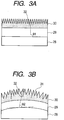
- FIGS. 3A and 3B are schematic cross-sectional views schematically illustrating an optical member according to the embodiment of the present invention in this case.
- the optical member of the present invention has a layer 29 containing an organic resin as a main component and a plate crystal layer 30 formed of a plate crystal containing aluminum oxide as a main component on the substrate 28.
- the surface of the plate crystal layer 30 has an uneven profile 31.
- the plate crystal layer 30 containing aluminum oxide as a main component are formed of a crystal containing an oxide or a hydroxide of aluminum or a hydrate thereof as a main component.
- Especially preferred crystals are boehmite.
- the plate crystals be selectively arranged with a predetermined angle to the surface of a layer for increasing the height of the fine unevenness and reducing the intervals therebetween.
- an oxide or hydroxide of aluminum, or a hydrate thereof is referred to as aluminum oxide.
- one or more oxide layers which contain aluminum oxide alone or any of ZrO 2 , SiO 2 , TiO 2 , ZnO, and MgO, and of which the amount of aluminum oxide is 70 mol% or more, may be referred to as a layer containing aluminum oxide as a main component.
- the surface of the substrate 28 is a flat surface such as flat plate, a film, or a sheet is shown in FIG. 3A .
- the plate crystal be arranged with respect to the surface layer of the substrate with an average angle of an angle ⁇ 1, between an inclination direction 32 of the plate crystal and the substrate surface, of 45° or more and 90° or less, and more preferably 60° or more and 90° or less.
- the plate crystal be arranged with respect to the surface layer of the substrate with an average angle of an angle ⁇ 2, between an inclination direction 32 of the plate crystal and the substrate surface, of 45° or more and 90° or less, and more preferably 60° or more and 90° or less. Note that there may be a case where the value of the angles ⁇ 1 and ⁇ 2 exceeds 90° depending on the gradient of the plate crystals. In this case, measurement is conducted so that the value is 90° or less.
- the thickness of the plate crystal layer 30 is preferably 20 nm or more and 1,000 nm or less, more preferably 50 nm or more and 1,000 nm or less. If the thickness of the layer forming the unevenness is 20 nm or more and 1,000 nm or less, an antireflection property owing to a fine uneven configuration is effective, the possibility that the mechanical strength of the unevenness is impaired is eliminated and the fine uneven configuration becomes advantageous in terms of manufacturing costs. By setting the thickness to 50 nm or more and 1,000 nm or less, the antireflection property is further improved, which is more preferred.
- the surface density of the fine unevenness of the present invention is also important, and the corresponding average surface roughness Ra' value obtained by two-dimensional extension of a center line average roughness is 5 nm or more, more preferably 10 nm or more, still more preferably 15 nm or more and 100 nm or less, and the surface area ratio Sr is 1.1 or more, more preferably 1.15 or more, still more preferably 1.2 or more and 3.5 or less.
- Ra' value is such a value that the center line average roughness Ra defined in JIS B 0601 is applied to a measurement surface and three-dimensionally extended, and the Ra' value is expressed as a "value obtained by averaging absolute values of deviations from a reference surface to a specified surface" and given by the following formula (1).
- Ra ′ 1 S 0 ⁇ Y B Y T ⁇ X L X R
- S surface area of an actual measurement surface).
- the surface area of an actual measurement surface is determined as follows. The measurement surface is divided into minute triangles consisting of the closest three data points (A, B, C), and then the area ⁇ S of each minute triangle is determined using a vector product.
- ⁇ S( ⁇ ABC) [s(s-AB)(s-BC)(s-AC)]0.5 (where AB, BC and AC are the lengths of the sides, and thus s ⁇ 0.5(AB+BC+AC)), and the total sum of the areas ⁇ S is a surface area S to be determined.
- Ra' as the surface density of the fine unevenness is 5 nm or more and Sr is 1.1 or more, antireflection owing to the uneven configuration can be realized. If Ra' is 10 nm or more and Sr is 1.15 or more, the antireflection effect becomes higher than that of the former case. If, Ra' is 15 nm or more and Sr is 1.2 or more, the uneven configuration has a performance capable of enduring practical use. However, if Ra' is 100 nm or more and Sr is 3.5 or more, the effect of scattering by the uneven configuration predominates over the antireflection effect so that a sufficient antireflection property cannot be obtained.
- the plate crystal layer 30 formed of a plate crystal containing aluminum oxide as a main component in the present invention is obtained by compounding an Al metal alone film or a metal film containing metal Al and one of metal Zn or metal Mg into the layer 29 containing an organic resin as a main component followed by soaking in hot water at 50°C or higher or exposure to water vapor. At this time, the uneven profile 31 is formed on the surface of the above metal due to hydration, dissolution, and redeposition.
- the plate crystal layer 30 can also be obtained by forming a layer containing aluminum oxide as a main component on the layer 29 containing an organic resin as a main component, and dissolving or depositing the surface selectively.
- the above layer containing aluminum oxide as a main component can be formed by a known vapor phase method such as CVD or PVD, a liquid phase method such as a sol-gel process, hydrothermal synthesis using an inorganic salt, or the like.
- a known vapor phase method such as CVD or PVD
- a liquid phase method such as a sol-gel process
- hydrothermal synthesis using an inorganic salt or the like.
- an amorphous aluminum oxide layer may remain in a lower portion of the uneven profile 31 in the plate crystal layer 30.
- a method of treating a gel film with hot water the gel film being formed by coating a sol-gel coating solution containing aluminum oxide to grow an alumina plate crystal, because a uniform antireflection layer can be formed on a substrate with a large area or on a non-planar substrate.
- an Al compound is used, or at least one of compounds of Zr, Si, Ti, Zn and Mg is used together with the Al compound.
- Al 2 O 3 , ZrO 2 , SiO 2 , TiO 2 , ZnO and MgO metal alkoxides of the respective metals and salt compounds such as chlorides and nitrates of the respective metals may be used.
- Metal alkoxides are preferably used in terms of film formability particularly for ZrO 2 , SiO 2 and TiO 2 raw materials.
- Aluminum compounds include, for example, aluminum ethoxide, aluminum isopropoxide, aluminum-n-butoxide, aluminum-sec-butoxide, aluminum-tert-butoxide, aluminum acetylacetnate or oligomers of these compounds, aluminum nitrate, aluminum chloride, aluminum acetate, aluminum phosphate, aluminum sulfate, and aluminum hydroxide.
- zirconium alkoxides include zirconilum tetramethoxide, zirconium tetraethoxide, zirconium tetra n-propoxide, zirconium tetraisopropoxide, zirconium tetra n-butoxide, and zirconium tetra-t-butoxide.
- R is the same or different lower alkyl group such as a methyl group, an ethyl group, a propyl group, an isopropyl group, a butyl group, or an isobutyl group.
- Titanium alkoxides include, for example, tetramethoxy titanate, tetraethoxy titanate, tetra n-propoxy titanate, tetraisopropoxy titanate, tetra n-butoxy titanate, and tetraisobutoxy titanate.
- Zinc compounds include, for example, zinc acetate, zinc chloride, zinc nitrate, zinc stearate, zinc oleate, and zinc salicylate, and especially preferred are zinc acetate and zinc chloride.
- Magnesium compounds include magnesium alkoxides such as magnesium dimethoxide, magnesium diethoxide, magnesium dipropoxide and magnesium dibutoxide, magnesium acetylacetate, and magnesium chloride.
- Organic solvents which may be any organic solvents which do not cause raw materials such as the above-mentioned alkoxides to gelate, include: for example, alcohols such as methanol, ethanol, 2-propanol, butanol, ethylene glycol, and ethylene glycol-mono-n-propyl ether; various kinds of aliphatic or alicyclic hydrocarbons such as n-hexane, n-octane, cyclohexane, cyclopentane, and cyclooctane; various kinds of aromatic hydrocarbons such as toluene, xylene, and ethyl benzene; various kinds of esters such as ethyl formate, ethyl acetate, n-butyl acetate, ethylene glycol monomethyl ether acetate, ethylene glycol monoethyl ether acetate, and ethylene glycol monobuthyl ether acetate; various kinds of keto
- alkoxide raw material particularly alkoxides of aluminum, zirconium, and titanium are highly reactive to water, and are abruptly hydrolyzed by addition of moisture in air or water, resulting in opacity and precipitation.
- Aluminum salt compounds, zinc salt compounds and magnesium salt compounds are hard to be dissolved in an organic solvent alone, and the stability of their solutions is low.
- a stabilizer is preferably added to stabilize the solution.
- Stabilizers may include, for example: ⁇ -diketone compounds such as acetyl acetone, dipyrobilemethane, trifluoroacetylacetone, hexafluoroacetylacetone, benzoylacetone, and dibenzoylmethane; ⁇ -ketoester compounds such as methyl acetoacetate, ethyl acetoacetate, allyl acetoacetate, benzyl acetoacetate, iso-propyl acetoacetate, tert-butyl acetoacetate, iso-butyl acetoacetate, 2-methoxyethyl acetoacetate, and 3-keto-n-methyl valeriate; and alkanol amines such as monoethanol amine, diethanol amine and triethanol amine.
- alkanol amines such as monoethanol amine, diethanol amine and triethanol amine.
- the amount of stabilizer added is preferably about 1 in terms of molar ratio to the alkoxide or salt compound.
- a catalyst is preferably added for the purpose of promoting part of the reaction in order to form an appropriate precursor.
- Catalysts may include, for example, nitric acid, hydrochloric acid, sulfuric acid, phosphoric acid, acetic acid, and ammonia.
- a known coating method such as a dipping method, a spin coating method, a spray method, a printing method, a flow coating method, and a combination thereof may be appropriately employed.
- the film After being coated with the above sol-gel coating solution, it is preferable to conduct heat-treatment in a range of 120°C or more and 230°C or less. As the temperature of heat treatment is higher, the film is likely to become more dense. However, when the temperature of the heat treatment exceeds 230°C, the damage such as deformation is caused in the substrate.
- the temperature of the heat treatment is more preferably 150°C or more and 210°C or less.
- the heating time is preferably 10 minutes or longer, although depending upon the heating temperature.
- a gel film which had undergone drying or heat treatment is immersed in hot water, whereby plate crystals containing aluminum oxide as a main component are precipitated to form an unevenness profile of the outermost surface.
- the surface layer of the gel film containing aluminum oxide undergoes a deflocculating action or the like, and some components are eluted, but due to a difference in solubility in hot water between various kinds of hydroxides, plate crystals containing aluminum oxide as a main component are precipitated on the surface layer of the gel film, and grow.
- the temperature of hot water is preferably 40°C to 100°C.
- the hot water treatment time is about 5 minutes to about 24 hours.
- the organic resin used in the layer 29 containing an organic resin as a main component of the present invention may have a function of adjusting the refractive index difference between the substrate 28 and the plate crystal layer 30 containing aluminum oxide as a main component, and may be transparent in a wavelength region of light to be used.
- the layer 29 containing an organic resin as a main component of the present invention adjusts the refractive index difference between the substrate 28 and the plate crystal layer 30 containing aluminum oxide as a main component, thereby contributing to the exhibition of high antireflection property. Therefore, it is desired that the layer 29 have an optimum film thickness and refractive index, and the optimum film thickness and refractive index are kept stably from the time when the film is produced.
- a layer containing 80% by weight or more of an organic resin may be referred to as a layer containing an organic resin as a main component.
- An organic resin having an aromatic ring and/or an imide ring in a main chain is used in the layer containing an organic resin as a main component of the present invention.
- An example of the aromatic ring or imide ring includes structures represented by the following chemical formulae.
- an aromatic ring or an imide ring has a planar structure
- molecular chains of an organic resin in which these structures are introduced in a main chain are likely to be aligned parallel to the substrate during the formation of a film. Therefore, even in the case where the organic resin layer 29 of the present invention having a film thickness of 10 nm or more and 150 nm or less is used, the uniformity of film thickness and refractive index is high. Further, in that case, solvent resistance is excellent, a glass transition temperature is high, heat resistance is excellent, and film thickness and refractive index are unlikely to change.
- the plate crystal layer 30 formed of plate crystals containing aluminum oxide as a main component a gel film containing the aluminum oxide is exposed to water vapor or is soaked in hot water. At this time, it is desired that the change in film thickness and refractive index of the organic resin layer be minimized.
- the organic resin layer 29 in which dissolution and swelling are unlikely to occur with hot water, unlike the organic resin having an aromatic ring and/or imide ring in a main chain. Further, the density of the film in the plate crystal layer is low, so moisture or the like from outside passes through the metal oxide layer easily and reaches the surface of the substrate.
- the layer 3 or 5 containing an organic resin as a main component of the present invention is desired to have an effect of blocking moisture and the like coming from outside via the plate crystal layer.
- an organic resin having a low percentage of water absorption Such an organic resin has a percentage of water absorption of 0.05% or more and 2% or less. When the organic resin has a percentage of water absorption of 2% or less, the organic resin can block moisture coming from outside.
- the percentage of water absorption as used herein refers to the percentage of water absorption of a film left at 23°C for 24 hours after the film is formed.
- an organic resin having a percentage of water absorption of less than 0.05% the adherence to the substrate is decreased remarkably. Therefore, even if pretreatment of the surface of the substrate is conducted, the organic resin is peeled off from the substrate during hot water treatment and the like.
- thermosetting resin any of a thermosetting resin and a thermoplastic resin can be used as long as it is an organic resin having an aromatic ring and/or an imide ring in a main chain.
- thermosetting resin include cured products of a compound or an oligomer having one or more reactive or polymerizable substituents, such as an epoxy group, an oxetanyl group, an episulphide group, a methylol group, an isocyanate group, a thioisocynate group, a vinyl ether group, an acryloyl group, a methacryloyl group, and a maleimide group.
- a cured resin obtained by mixing two or more kinds of compounds having different reactive or polymerizable substituents or oligomers, followed by curing can be used.
- the cured resin having an aromatic ring and/or an imide ring in a main chain include a cured product of bisphenol A epoxy, a cured product of m-phenylenediisocyanate, and cured products of a methylomelamine resin, a guanamine resin, and a maleimide resin.
- an initiator and a curing agent can be used together when the above compound is cured.
- the initiator is mostly selected from radical, cation, and anion initiators depending upon the reactivity of a substituent of the above compound.
- a thermal decomposition type initiator is widely used. Examples of the thermal decomposition type initiator include N,N-azobisbutyronitrile as a radical initiator, and pyridinium p-toluenesulfonate as a cation initiator.
- an organic acid such as p-toluenesulfonic acid as a cation initiator and an organic amine such as diazabicycloundecene as an anion initiator may be mixed in small amounts.
- a photosensitive initiator is used in the case of conducting curing with light such as UV-light.
- thermoplastic resin having an aromatic ring and/or an imide ring in a main chain examples include aromatic polyethers such as polyether ketone and polyether sulfone, aromatic polyesters such as polyethylene terephthalate, aromatic polycarbonate, aromatic polyurethane, aromatic polyurea, aromatic polyamide, and thermoplastic polyimide.
- aromatic polyethers, aromatic polysulfides, polycarbonate, and thermoplastic polyimides are preferred in terms of heat resistance.
- thermoplastic resin is more preferred since a refractive index and a film thickness do not change under baking conditions, and less uncured monomer remains.
- an organic resin containing siloxane structure (-SiR 2 -O-) m , where R is a methyl group or a phenyl group, and m is an integer of 1 to 6.
- the repeating unit including (-SiR 2 O-) m is preferably 30 mol% or less based on the whole repeating units. When it is 30 mol% or more, heat resistance is decreased due to the decrease in glass transition temperature, and wettability with respect to a glass substrate is decreased.
- the refractive index of the layer 2 or 5 containing the organic resin as a main component can be changed. For example, by increasing the number of aromatic rings contained in the organic resin and the number of hetero rings contained therein, the refractive index is enhanced. On the other hand, by increasing an aliphatic chain, an alicyclic structure, the above siloxane structure and fluoroalkyl group, etc., transparency is enhanced, and the refractive index is decreased.
- examples of the organic resins whose refractive indices are changed relatively easily depending on the structure include polyimide, aromatic polyethers, aromatic polysulfides, and aromatic polycarbonate. These polymers can introduce the above structure into a main chain or a side chain together with an aromatic ring and an imide ring via a monomer.
- Polyimide is synthesized generally by polyaddition reaction and dehydration-condensation reaction between a dianhydride and a diamine.
- a transparent polyimide in a visible light region is obtained.
- dianhydride having an alicyclic structure and introducing one or a plurality of various kinds of structures such as siloxane structure, an aliphatic chain, an alicyclic structure, and an aromatic ring into diamine, the refractive index can be changed arbitrarily from 1.5 to 1.7.
- a dianhydride used for the synthesis of thermoplastic polyimide examples include: aromatic acid dianhydrides such as pyromellitic dianhydride, 3,3'-biphthalic anhydride, 3,4'-biphthalic anhydride, 3,3',4,4'-benzophenonetetracarboxylic dianhydride, 3,3',4,4'-diphenylsulfonetetracarboxylic dianhydride, 4,4'-(hexafluoroisopropylidene)diphthalic anhydride, and 4,4'-oxydiphthalic dianhydride; and aliphatic acid dianhydrides such as meso-butane-1,2,3,4-tetracarboxylic dianhydride, 1,2,3,4-cyclobutanecarboxylic dianhydride, 1,2,3,4-cyclopentanetetracarboxylic dianhydride, 1,2,4,5-cyclohexanetetracarboxylic dianhydride,
- thermoplastic polyimide examples include: aromatic diamines such as m-phenylenediamine, p-phenylenediamine, 3,4'-diaminodiphenylmethane, 4,4'-diaminodiphenylmethane, 4,4'-diamino-3,3'-dimethyldiphenylmethane, o-tolidine, m-tolidine, 4,4'-diaminobenzophenone, 1,1-bis(4-aminophenyl)cyclohexane, 3,4'-diaminodiphenyl ether, 4,4'-diaminodiphenyl ether, 1,4-bis(4-aminophenoxy)benzene, 1,3-bis(4-aminophenoxy)benzene, 2,2-bis[4-(4-aminophenoxy)phenyl]propane, 4,4'-bis(4-aminophenoxy)
- At least -SiR 2 -O- group-containing diamines such as 1,3-bis(3-aminopropyl)tetramethyldisiloxane and 1,4-bis(3-aminopropyldimethylsilyl)benzene.
- the aromatic polyethers are synthesized generally by subjecting a bisphenol and an aromatic dihalide to condensation reaction in a solvent in the presence of a base such as potassium carbonate.
- a base such as potassium carbonate.
- aromatic polysulfide is synthesized.
- Examples of the bisphenol used for the synthesis of aromatic polyether include resorcinol, hydroquinone, 4,4'-biphenol, 2,2-bis(4-hydroxyphenyl)propane, 4,4'-dihydroxydiphenylmethane, 1,1-bis(4-hydroxyphenyl)cyclohexane, 1,1-bis(4-hydroxy-3-methylphenyl)cyclohexane, 4,4'-(1- ⁇ -methylbenzylidene)bisphenol, 1,3-bis[2-(4-hydroxyphenyl)-2-propyl]benzene, ⁇ , ⁇ '-bis(4-hydroxyphenyl)-1,4-diisopropylbenzene, ⁇ , ⁇ '-bis(4-hydroxy-3,5-dimethylphenyl)-1,4-diisopropylbenzene, 9,9-bis(4-hydroxyphenyl)fluorene, 9,9-bis(4-hydroxy-3-methylphenyl)fluorene, 4,
- aromatic disulfide used for the synthesis of aromatic polysulfide examples include p-benzenedithiol, m-benzenedithiol, 4,4'-oxybisbenzenethiol, 4,4'-thiobisbenzenethiol, and 4,4'-biphenyldithiol.
- aromatic dihalide used for the synthesis of aromatic polyether or aromatic polysulfide examples include 4,4'-dichlorobenzophenone, 4,4'-difluorobenzophenone, 4,4'-dichlorophenyl sulfone, bis(4-fluorophenyl)sulfone, bis(4-fluoro-3-nitrophenyl)sulfone, 2,6-dichlorobenzonitrile, 2,6-difluorobenzonitrile, 2,4-difluorobenzonitrile, tetrafluoroisophthalonitrile, perfluorobiphenyl, and 3,5-dichloro-1-methoxytriazine.
- dihalide dinitro compounds such as 2,4-dinitrobenzonitrile and 2,6-dinitrobenzonitrile may be used.
- the aromatic polycarbonate is synthesized generally by a method of allowing bisphenol to react with phosgene in a solution, or a method of allowing bisphenol to react with a carbonate such as diphenyl carbonate in a melt state.
- the refractive index can be changed arbitrarily from 1.5 to 1.65.
- bisphenol used for synthesizing aromatic polycarbonate bisphenol used for synthesizing the above aromatic polyether is used.
- aliphatic diol and aliphatic disulfide can be used together with aromatic polyether, aromatic polysulfide, and aromatic polycarbonate.
- a compound having one or more o-hydroxyphenoxypropylsiloxy groups be substituted for a part of bisphenol or aromatic disulfide.
- a (-SiR 2 -O-) n group can be introduced into a resin, whereby the adherence with respect to a substrate is enhanced.
- the refractive index ni of the layer 29 containing an organic resin as a main component of the present invention satisfy nb ⁇ ni ⁇ ns with respect to the refractive index nb of the substrate 25 and the refractive index ns of the plate crystal layer 30 formed of plate crystal containing the aluminum oxide as a main component. It is preferred to select an organic resin or a structure in the organic resin as such. By adjusting ni in this range, a high antireflection property can be exhibited.
- the layer 29 containing an organic resin as a main component can contain a silane coupling agent in addition to the organic resin so that adherence can be enhanced.
- inorganic fine particles such as SiO 2 , TiO 2 , ZrO 2 , SiO 2 , ZnO, MgO, and Al 2 O 3 can be mixed in a small amount.
- the amount of components other than the organic resin, which can be mixed is less than 20 parts by weight based on 100 parts by weight of the entire organic resin layer, and when the components are mixed in an amount exceeding 20 parts by weight, there is a possibility that transparency and uniformity of a film thickness may be impaired.
- thermoplastic resin can be used by dissolving it in an organic solvent alone or together with a component other than an organic resin.
- a thermoplastic resin precursor can be used by dissolving it in an organic solvent. In the case of the latter, the process of converting the precursor into a thermoplastic resin is required.
- Examples of an organic solvent used for forming the layer 29 containing an organic resin as a main component of the present invention include: ketones such as 2-butanone, methylisobutyl ketone, cyclopentanone, and cyclohexanone; esters such as ethyl acetate, n-butyl acetate, ethyleneglycol monomethylether acetate, propyleneglycol monomethylether acetate, and ethyl lactate; ethers such as tetrahydrofuran, dioxane, and diisopropyl ether; various aromatic hydrocarbons such as toluene, xylene, and ethylbenzene; chlorinated hydrocarbons such as chloroform, methylene chloride, and tetrachloroethane; and solvents such as N-methylpyrrolidone, N,N-dimethylformamide, N,N-dimethylacetamide, dimethyl sulfoxide, and
- known coating means can be appropriately used, such as dipping, spin coating, spraying, printing, flow coating, and a combination thereof.
- the thickness of the layer 29 of the present invention containing an organic resin as a main component is 10 nm or more and 150 nm or less, more preferably 20 nm or more and 100 nm or less. If the thickness is less than the range, it is difficult to form a uniform coating, and desirable optical characteristics cannot be obtained. If the thickness is greater than the range, contribution to the reflection reducing effect is reduced due to interference and the like.
- the substrate used in the present invention is glass. Substrates in other arrangements not forming part of the present invention may include resins, glass mirrors and mirrors formed of resin.
- resin substrate include films and molded products of thermoplastic resins, such as polyester, triacetyl cellulose, cellulose acetate, polyethylene terephthalate, polypropylene, polystyrene, polycarbonate, polysulfone, polyacrylate, polymethacrylate, an ABS resin, polyphenylene oxide, polyurethane, polyethylene, polycycloolefin, and polyvinyl chloride; cross-linked films and cross-linked molded products obtained from various kinds of thermosetting resins, such as an unsaturated polyester resin, a phenol resin, a cross-linked polyurethane, a cross-linked acryl resin, and a cross-linked saturated polyester resin.
- thermoplastic resins such as polyester, triacetyl cellulose, cellulose acetate, polyethylene terephthalate, polypropylene, polystyren
- glass may include no alkali glass and alumina silicate glass.
- Substrates for use in the present invention which may be formed of any glass materials capable of being finally formed into a shape according to a use purpose, include flat plates, films, and sheets, and may have a two-dimensional or three-dimensional curved surface. The thickness can be appropriately determined, and is generally 5 mm or less, but is not limited thereto.
- the optical transparent element of the present invention may be further provided with a layer for imparting various kinds of functions, in addition to the layers described above.
- a hard coat layer may be provided on the layer of plate crystals for improving the hardness of the film, or a water-repellent layer of fluoroalkyl silane or alkyl silane may be provided for imparting water repellency.
- a layer of a material having a refractive index lower than that of plate crystals containing aluminum oxide as a main component, or a layer formed of an amphipathic compound may be provided.
- an adhesive layer or a primer layer may be used for improving the adherence between the substrate and the layer containing an organic resin as a main component.
- Diamine (1), diamine (2), and diamine (3) in an amount of 0.012 mol in total were dissolved in N,N-dimethylacetamide (hereinafter, abbreviated as DMAc). While the diamine solution was cooled with water, 0.12 mol of acid dianhydride was added thereto. The amount of DMAc was set so that the total mass of diamine and acid dianhydride became 20% by weight. The solution was stirred at room temperature for 15 hours, whereby a polymerization reaction was performed. After the solution was diluted with DMAc so as to be 8% by weight, and 7.4 ml of pyridine and 3.8 ml of acetic anhydride were added to the resultant solution, followed by stirring at room temperature for 1 hour.
- DMAc N,N-dimethylacetamide
- thermosetting resin solution 12 5 g of melamine resin (NIKALAC MX-750LM (Trade Name) manufactured by Nippon Carbide Industries Co., Inc.) and 0.025 g of p-toluene sulfonic acid were dissolved in 95 g of 1-methoxy-2-propanol to prepare thermosetting resin solution 12.
- a mixed solvent of 3.15 g of 0.01 M diluted hydrochloric acid [HClaq.] and 29.5 g of 1-butanol/2-propanol (hereinafter, abbreviated as IPA) at a ratio of 1/1 (wt.) was added slowly to 14.6 g of ethyl silicate, and stirred at room temperature. After stirring for 6 hours, the resultant mixture was diluted with 92.5 g of a mixed solvent of 1-butanol/IPA at a ratio of 1/1 (wt.) to obtain an A-solution.
- IPA 1-butanol/2-propanol
- pellet-shaped polysulfone (Mn of 16,000 or more, manufactured by Sigma-Aldrich Corp.) was dissolved in 10 g of ⁇ -butyrolactone to prepare a polysulfone solution 18.
- polystyrene solution 19 2.5 g of powder of polystyrene (manufactured by Sigma-Aldrich Corp.) was dissolved in 10 g of cyclohexanone to prepare a polystyrene solution 19.
- a coating film of various kinds of organic resins was formed on a silicon substrate and sintered at 200°C for 60 minutes. After that, the water absorption amount of the film after being soaked in ion-exchanged water at 23°C for 24 hours was measured with a thermogravimetric apparatus (TG/TDA, Thermo plus 2 manufactured by Rigaku Corporation) to obtain the water absorption ratio of the film.
- TG/TDA thermogravimetric apparatus
- the surface of a surface layer of a coating was photographically observed (acceleration voltage; 10.0 kV, magnification; 30,000) using a scanning electron microscope (FE-SEM, S4500 manufactured by Hitachi Ltd.).
- a transmittance was measured over a range of 350 nm to 850 nm using an automatic optical member measuring apparatus (V-570 manufactured by JASCO). A disc glass plate was used. The angle of incidence of light in measurements of transmittance was 0°.
- Measurements were made over a range of wavelengths from 380 nm to 800 nm by a spectral ellipsometer (VASE manufactured by J. A. Woollam JAPAN Co., Inc.).
- an alumina sol solution 14 was dropped onto one surface of the substrate with the film of the polyimide 1, followed by spin coating at 4, 000 rpm for 20 seconds and pre-drying at 80°C for 10 minutes. The other surface was similarly spin coated with the alumina sol solution. After that, the resultant substrate was sintered in a hot air circulation oven at 200°C for 30 minutes, whereby the substrate was covered with transparent amorphous Al 2 O 3 films.
- the substrate was soaked in hot water at 80°C for 30 minutes, and dried at 60°C for 10 minutes.
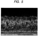
- the surface of the obtained film was observed by the FE-SEM to find a fine uneven structure in which plate crystals containing Al 2 O 3 as a main component were tangled randomly and complicatedly as shown in FIG. 4 .
- a plate crystal layer containing Al 2 O 3 as a main component was arranged selectively with an average angle of 75° with respect to the surface of the substrate.
- the film thickness and the refractive index were measured using ellipsometry.
- the thickness and the refractive index of each film are shown in Table 3.
- Example 2 The same operation as in Example 1 was conducted except for using the polyimide solution 7 in place of the polyimide solution 6 to form an organic resin layer formed of the polyimide 2.
- Example 3 The same operation as in Example 3 was conducted except for using the polyimide solution 8 in place of the polyimide solution 7 to form an organic resin layer formed of the polyimide 3.
- Example 3 The same operation as in Example 3 was conducted except for using the polyimide solution 9 in place of the polyimide solution 7 to form an organic resin layer formed of the polyimide 4.
- the resultant substrate was sintered in a hot air circulation oven at 200°C for 60 minutes, whereby a substrate with an organic resin layer formed of bisphenol Z polycarbonate was produced.
- Table 2 shows the film thickness, refractive index, and percentage of water absorption of the thermosetting resin film.
- Example 2 a transparent amorphous Al 2 O 3 film was coated in the same way as in Example 1, and evaluated.
- thermosetting resin solution 12 in place of the polycarbonate solution 11 to form an organic resin layer formed of a thermosetting resin.
- Example 8 The same operation as in Example 8 was conducted except for using the polyimide solution 9 in place of the polyimide solution 8 to form the organic resin layer formed of the polyimide 4.
- an alumina sol solution 15 was dropped onto one surface of the substrate with the film of the polyimide 2, followed by spin coating at 2, 700 rpm for 20 seconds and pre-drying at 80°C for 10 minutes.
- the other surface was similarly spin coated with the alumina sol solution 15.
- the resultant substrate was sintered in a hot air circulation oven at 200°C for 10 minutes.
- both surfaces were coated again with the alumina sol solution 15 by the same method, and the substrate was finally sintered at 200°C for 30 minutes, whereby the substrate was covered with transparent amorphous Al 2 O 3 films.
- the substrate was soaked in hot water at 80°C for 30 minutes, and dried at 60°C for 10 minutes.
- Example 14 The same operation as in Example 14 was conducted except for using the polycarbonate solution 11 in place of the polyimide solution 9 to form an organic resin layer formed of polycarbonate.
- Example 6 The same operation as in Example 6 was conducted except for using the polyether ether ketone solution 17 in place of the polycarbonate solution 11 to form an organic resin layer formed of polyether ether ketone.
- Example 6 The same operation as in Example 6 was conducted except for using the polysulfone solution 18 in place of the polycarbonate solution 11 to form an organic resin layer formed of polysulfone.
- the substrate was soaked in hot water at 80°C for 30 minutes, and dried at 60°C for 10 minutes.
- an antireflection film was formed by the same method as that in Example 1 after covering the substrate with the amorphous Al 2 O 3 films, and evaluation was conducted.
- Example 6 The same operation as in Example 6 was conducted except for using the polystyrene solution 19 in place of the polycarbonate solution 11 to form an organic resin layer formed of polystyrene.
- the substrate was soaked in hot water after being covered with the amorphous Al 2 O 3 films, film peeling occurred from an organic intermediate layer, with the result that an antireflection film was not obtained.
- FIG. 6 is a front view of an optical member of Example 16.
- an optical member 1 is a concave lens
- a substrate 2 is provided with an optical member 3.
- FIG. 7 illustrates a cross-section of the optical member of Example 18 cut taken along the 7-7 section in FIG. 6 .
- a layer containing an organic resin as a main component, and a layer having arranged plate crystals containing aluminum oxide as a main component are formed on an optical surface, and an optical member 3 having an uneven profile is formed on the outermost surface, whereby reflection of light at the optical surface is reduced.
- the optical member is a concave lens, but the present invention is not limited thereto, and the lens may be either a convex lens or a meniscus lens.
- FIG. 8 is a front view of an optical member of Example 19.
- an optical member 1 is a prism
- a base body 2 is provided with an optical member 3.
- FIG. 9 shows a cross-section of the optical member of Example 19 cut taken along the 9-9 section in FIG. 8 .
- a layer containing an organic resin as a main component, and a layer having arranged plate crystals containing aluminum oxide as a main component are formed on an optical surface, and the optical member 3 having an uneven profile is formed on the outermost surface, whereby reflection of light at the optical surface is reduced.
- angles formed by optical surfaces of the prism are 90°C and 45°C, but the present invention is not limited thereto, and the optical surfaces of the prism may form any angle.
- FIG. 10 is a front view of an optical member of Example 20 of the present invention.
- an optical member 1 is a fly eye integrator, and a substrate 2 is provided with an optical member 3.
- FIG. 11 shows a cross-section of an optical member of Example 20 cut taken along the 11-11 section in FIG. 10 .
- a layer containing an organic resin as a main component, and a layer having arranged plate crystals containing aluminum oxide as a main component are formed on an optical surface, and an optical member 3 having an uneven profile is formed on the outermost surface, whereby reflection of light at the optical surface is reduced.
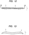
- FIG. 12 is a front view of an optical member of Example 21 of the present invention.
- an optical member 1 is an f ⁇ lens
- a substrate 2 is provided with an optical member 3.
- FIG. 13 illustrates a cross-section of an optical member of Example 21 cut taken along the 13-13 section in FIG. 12 .
- a layer containing an organic resin as a main component, and a layer having arranged plate crystals containing aluminum oxide as a main component are formed on an optical surface, an the optical member 3 having an uneven profile is formed on the outermost surface, whereby reflection of light at the optical surface is reduced.
- FIG. 14 illustrates a cross-section of one of a pair of optical systems of a binocular.
- reference numeral 4 denotes an objective lens
- reference numeral 5 denotes a prism (shown in an exposed form) for inverting an images
- reference numeral 6 denotes an eye lens
- reference numeral 7 denotes an image formation surface
- reference numeral 8 denotes a pupil surface (evaluation surface).
- reference numeral 3 (shown with a legend) denotes an optical transparent element relating to the present invention.
- a layer containing an organic resin as a main component, and a layer having arranged plate crystals containing aluminum oxide as a main component are formed, and the outermost surface has an uneven profile, whereby reflection of light at each optical surface is reduced.
- the optical member 3 formed of a fine uneven configuration is provided neither on an optical surface 9 of the objective lens closest to an object nor on an optical surface 10 of the eye lens closest to the evaluation surface.
- the reason why the optical member 3 is not provided on these surfaces is that its performance will be degraded due to contact while it is used, but the present invention is not limited thereto, and the optical member 3 may be provided on the optical surfaces 9 and 10.
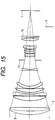
- FIG. 15 illustrates a cross-section of a photographing lens (telephoto lens is illustrated in this figure) of a camera or the like.
- reference numeral 7 denotes a film as an image formation surface, or a solid imaging device (photoelectric conversion element) such as a CCD or a CMOS
- reference numeral 11 denotes a diaphragm
- reference numeral 3 (shown with a legend) denotes an optical member relating to the present invention.
- a layer containing an organic resin as a main component, and a layer having arranged plate crystals containing aluminum oxide as a main component are formed, and the outermost surface has an uneven profile, whereby reflection of light at each optical surface is reduced.
- the optical member 3 formed of a fine uneven configuration is not provided on an optical surface 9 of the objective lens closest to an object. The reason why the optical member 3 is not provided on the surface is that its performance will be degraded due to contact while it is used, but the present invention is not limited thereto, and the optical member 3 may be provided on the optical surface 9.
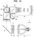
- FIG. 16 illustrates a cross-section of a projector optical system.
- reference numeral 12 denotes a light source
- reference numerals 13a and 13b denote fly eye integrators
- reference numeral 14 denotes a polarizing conversion element
- reference numeral 15 denotes a condenser lens
- reference numeral 16 denotes a mirror
- reference numeral 17 denotes a field lens
- reference numerals 18a, 18b, 18c and 18d denote prisms
- reference numerals 19a, 19b and 19c denote light modulation elements
- reference numeral 20 denotes a projection lens.
- reference numeral 3 (shown with a legend) denotes an optical transparent element relating to the present invention.
- a layer containing an organic resin as a main component, and a layer having arranged plate crystals containing aluminum oxide as a main component are formed, and the outermost surface has an uneven profile, whereby reflection of light at each optical surface is reduced.
- the optical member 3 of this example is configured to contain an inorganic component such as silica or alumina as a main component, the optical member has a high heat resistance, and never suffers from a degradation in performance even if placed at a position 13a so close to the light source 12 that the optical member 3 is exposed to high heat.
- an inorganic component such as silica or alumina
- Example 25 of the present invention An example in which the optical member of the present invention is used in a scan optical system (laser beam printer) is shown as Example 25 of the present invention.
- FIG. 17 illustrates a cross-section of a scan optical system.
- reference numeral 12 denotes a light source
- reference numeral 21 denotes a collimator lens
- reference numeral 11 denotes an aperture diaphragm
- reference numeral 22 denotes a cylindrical lens
- reference numeral 23 denotes a light deflector
- reference numerals 24a and 24b denote f ⁇ lenses
- reference numeral 7 denotes an image surface.
- reference numeral 3 (shown with a legend) denotes an optical transparent element relating to the present invention.
- a layer containing an organic resin as a main component, and a layer having arranged plate crystals containing aluminum oxide as a main component are formed, and the outermost surface has an uneven profile, whereby reflection of light at each optical surface is reduced to realize formation of high-quality images.
- the optical member of the present invention can be adapted to a transparent substrate having any refractive index, shows an excellent antireflection effect to visible light, and has a long-term weather resistance, and therefore it can be used for various kinds of displays of word processors, computers, televisions, plasma display panels, and the like; optical members such as polarizing plates of liquid crystal apparatuses, sunglass lenses, graduated eyeglass lenses, finder lenses for cameras, prisms, fly-eye lenses, toric lenses, various kinds of optical filters, sensors and the like, which are formed of various kinds of optical glass materials; and further, photographic optical systems using those optical members, observation optical systems such as binoculars, projection optical systems for use in liquid crystal projectors, various optical lenses of scan optical systems for use in laser printers and the like, covers of various kinds of instruments, and window glasses of automobiles, electric trains, and the like.
- optical members such as polarizing plates of liquid crystal apparatuses, sunglass lenses, graduated eyeglass lenses, finder lenses for cameras, prisms, fly-eye lenses, toric lenses
Landscapes
- Chemical & Material Sciences (AREA)
- Physics & Mathematics (AREA)
- Engineering & Computer Science (AREA)
- Life Sciences & Earth Sciences (AREA)
- Chemical Kinetics & Catalysis (AREA)
- Materials Engineering (AREA)
- Organic Chemistry (AREA)
- Optics & Photonics (AREA)
- General Physics & Mathematics (AREA)
- General Chemical & Material Sciences (AREA)
- Geochemistry & Mineralogy (AREA)
- Wood Science & Technology (AREA)
- Crystallography & Structural Chemistry (AREA)
- Surface Treatment Of Optical Elements (AREA)
- Laminated Bodies (AREA)
Applications Claiming Priority (4)
| Application Number | Priority Date | Filing Date | Title |
|---|---|---|---|
| JP2007040003 | 2007-02-20 | ||
| JP2008033290A JP4639241B2 (ja) | 2007-02-20 | 2008-02-14 | 光学用部材、それを用いた光学系及び光学用部材の製造方法 |
| PCT/JP2008/053129 WO2008102902A1 (ja) | 2007-02-20 | 2008-02-19 | 光学用部材、それを用いた光学系及び光学用部材の製造方法 |
| EP08711893.1A EP2113797B1 (en) | 2007-02-20 | 2008-02-19 | Optical member, optical system using the same, and method for producing optical member |
Related Parent Applications (2)
| Application Number | Title | Priority Date | Filing Date |
|---|---|---|---|
| EP08711893.1A Division EP2113797B1 (en) | 2007-02-20 | 2008-02-19 | Optical member, optical system using the same, and method for producing optical member |
| EP08711893.1A Division-Into EP2113797B1 (en) | 2007-02-20 | 2008-02-19 | Optical member, optical system using the same, and method for producing optical member |
Publications (2)
| Publication Number | Publication Date |
|---|---|
| EP2977794A1 EP2977794A1 (en) | 2016-01-27 |
| EP2977794B1 true EP2977794B1 (en) | 2018-10-31 |
Family
ID=39710172
Family Applications (2)
| Application Number | Title | Priority Date | Filing Date |
|---|---|---|---|
| EP15180511.6A Active EP2977794B1 (en) | 2007-02-20 | 2008-02-19 | Optical member, optical system using the optical member, and method of manufacturing an optical member |
| EP08711893.1A Active EP2113797B1 (en) | 2007-02-20 | 2008-02-19 | Optical member, optical system using the same, and method for producing optical member |
Family Applications After (1)
| Application Number | Title | Priority Date | Filing Date |
|---|---|---|---|
| EP08711893.1A Active EP2113797B1 (en) | 2007-02-20 | 2008-02-19 | Optical member, optical system using the same, and method for producing optical member |
Country Status (5)
| Country | Link |
|---|---|
| US (5) | US7771832B2 (enExample) |
| EP (2) | EP2977794B1 (enExample) |
| JP (1) | JP4639241B2 (enExample) |
| CN (1) | CN101646960B (enExample) |
| WO (1) | WO2008102902A1 (enExample) |
Families Citing this family (61)
| Publication number | Priority date | Publication date | Assignee | Title |
|---|---|---|---|---|
| US7114990B2 (en) | 2005-01-25 | 2006-10-03 | Corning Gilbert Incorporated | Coaxial cable connector with grounding member |
| US8501270B2 (en) * | 2005-02-18 | 2013-08-06 | Canon Kabushiki Kaisha | Optical transparent member and optical system using the same |
| JP4639241B2 (ja) | 2007-02-20 | 2011-02-23 | キヤノン株式会社 | 光学用部材、それを用いた光学系及び光学用部材の製造方法 |
| JPWO2009116397A1 (ja) * | 2008-03-18 | 2011-07-21 | 株式会社きもと | 光学部材及びそれを用いたバックライト装置 |
| JP2010072046A (ja) * | 2008-09-16 | 2010-04-02 | Canon Inc | 光学素子及びそれを有する光学装置 |
| JP5511313B2 (ja) * | 2008-11-07 | 2014-06-04 | キヤノン株式会社 | 光学素子成形用金型、光学素子成形用金型の製造方法、光学素子、および光学素子の製造方法 |
| JP5814512B2 (ja) * | 2009-03-31 | 2015-11-17 | キヤノン株式会社 | 光学用部材、その製造方法及び光学系 |
| JP5511307B2 (ja) | 2009-10-23 | 2014-06-04 | キヤノン株式会社 | 光学部材、及びその製造方法 |
| TWI408331B (zh) * | 2009-12-17 | 2013-09-11 | Ind Tech Res Inst | 雙面光學膜片量測裝置與方法 |
| JP4991943B2 (ja) | 2010-02-26 | 2012-08-08 | キヤノン株式会社 | 光学用部材、ポリイミド、およびその製造方法 |
| TWI549386B (zh) | 2010-04-13 | 2016-09-11 | 康寧吉伯特公司 | 具有防止進入及改良接地之同軸連接器 |
| JP5279858B2 (ja) * | 2010-05-07 | 2013-09-04 | キヤノン株式会社 | 酸化アルミニウム前駆体ゾル、および光学用部材の製造方法 |
| JP2012073590A (ja) * | 2010-08-31 | 2012-04-12 | Canon Inc | 光学部材、その製造方法及び光学系 |
| JP5552007B2 (ja) * | 2010-09-17 | 2014-07-16 | 富士フイルム株式会社 | 光電場増強デバイス |
| JP5553717B2 (ja) * | 2010-09-17 | 2014-07-16 | 富士フイルム株式会社 | 光電場増強デバイスを用いた光の測定方法および測定装置 |
| JP5641851B2 (ja) | 2010-09-30 | 2014-12-17 | キヤノン株式会社 | 光学膜製造用塗布液、その製造方法および光学膜の製造方法 |
| JP5932222B2 (ja) | 2011-01-19 | 2016-06-08 | キヤノン株式会社 | 光学用部材及びその製造方法 |
| US20120207973A1 (en) * | 2011-02-15 | 2012-08-16 | Canon Kabushiki Kaisha | Optical member, method of manufacturing the same, and optical system using the same |
| JP5647924B2 (ja) * | 2011-03-18 | 2015-01-07 | 富士フイルム株式会社 | 光学部材の製造方法 |
| JP5801587B2 (ja) * | 2011-03-31 | 2015-10-28 | 富士フイルム株式会社 | 光電場増強デバイスの製造方法 |
| EP2696220A4 (en) * | 2011-03-31 | 2014-10-01 | Sony Corp | PRINTED MATERIAL AND PHOTOGRAPHIC MATERIAL |
| JP5936444B2 (ja) * | 2011-07-26 | 2016-06-22 | キヤノン株式会社 | 光学素子、それを用いた光学系および光学機器 |
| US20130072057A1 (en) | 2011-09-15 | 2013-03-21 | Donald Andrew Burris | Coaxial cable connector with integral radio frequency interference and grounding shield |
| US9136654B2 (en) | 2012-01-05 | 2015-09-15 | Corning Gilbert, Inc. | Quick mount connector for a coaxial cable |
| JP6433110B2 (ja) * | 2012-02-10 | 2018-12-05 | キヤノン株式会社 | 光学用部材及びその製造方法 |
| US9407016B2 (en) | 2012-02-22 | 2016-08-02 | Corning Optical Communications Rf Llc | Coaxial cable connector with integral continuity contacting portion |
| EP2644661B1 (en) | 2012-03-29 | 2018-12-05 | Canon Kabushiki Kaisha | Precursor sol of aluminum oxide and method for manufacturing the same, method for manufacturing optical member, optical member, and optical system |
| EP2645136B1 (en) | 2012-03-29 | 2017-01-18 | Canon Kabushiki Kaisha | Optical member having textured structure and method of producing same |
| JP5950667B2 (ja) * | 2012-04-16 | 2016-07-13 | キヤノン株式会社 | 光学用部材、その製造方法および光学用部材の光学膜 |
| JP2014006496A (ja) * | 2012-05-30 | 2014-01-16 | Canon Inc | 光学部材、撮像装置及び光学部材の製造方法 |
| JP5885595B2 (ja) * | 2012-06-12 | 2016-03-15 | キヤノン株式会社 | 反射防止膜、および、それを有する光学素子、光学系、光学機器 |
| US9287659B2 (en) | 2012-10-16 | 2016-03-15 | Corning Optical Communications Rf Llc | Coaxial cable connector with integral RFI protection |
| JP6164824B2 (ja) * | 2012-11-30 | 2017-07-19 | キヤノン株式会社 | 光学用部材及びその製造方法 |
| JP5885649B2 (ja) | 2012-12-20 | 2016-03-15 | キヤノン株式会社 | 反射防止膜を有する光学素子、光学系および光学機器 |
| FR3000487B1 (fr) * | 2012-12-28 | 2015-02-13 | Saint Gobain | Substrat transparent, notamment substrat verrier, revetu par au moins une couche poreuse au moins bifonctionnelle, procede de fabrication et applications |
| US20140252619A1 (en) * | 2013-03-08 | 2014-09-11 | Taiwan Semiconductor Manufacturing Company, Ltd. | Interconnect structure that avoids insulating layer damage and methods of making the same |
| US10290958B2 (en) | 2013-04-29 | 2019-05-14 | Corning Optical Communications Rf Llc | Coaxial cable connector with integral RFI protection and biasing ring |
| CN105284015B (zh) | 2013-05-20 | 2019-03-08 | 康宁光电通信Rf有限责任公司 | 具有整体rfi保护的同轴电缆连接器 |
| US9548557B2 (en) * | 2013-06-26 | 2017-01-17 | Corning Optical Communications LLC | Connector assemblies and methods of manufacture |
| US20170176644A1 (en) * | 2013-11-27 | 2017-06-22 | Canon Kabushiki Kaisha | Optical member and method for manufacturing the same |
| EP3077856A1 (en) * | 2013-12-03 | 2016-10-12 | Vertu Corporation Limited | Optical element with sapphire layer |
| JP2015194691A (ja) * | 2014-03-24 | 2015-11-05 | パナソニックIpマネジメント株式会社 | 複合光学素子及び複合光学素子用光学材料 |
| JP5805274B2 (ja) * | 2014-06-25 | 2015-11-04 | キヤノン株式会社 | レンズの製造方法 |
| JP6362105B2 (ja) | 2014-08-27 | 2018-07-25 | キヤノン株式会社 | 反射防止膜を有する光学素子、光学系、光学機器 |
| JP2016062014A (ja) * | 2014-09-19 | 2016-04-25 | 日本碍子株式会社 | 光学部品 |
| US9548572B2 (en) | 2014-11-03 | 2017-01-17 | Corning Optical Communications LLC | Coaxial cable connector having a coupler and a post with a contacting portion and a shoulder |
| TWI545078B (zh) * | 2014-11-25 | 2016-08-11 | 華碩電腦股份有限公司 | 具有蛾眼結構之基板及其製作方法 |
| US9590287B2 (en) | 2015-02-20 | 2017-03-07 | Corning Optical Communications Rf Llc | Surge protected coaxial termination |
| US10033122B2 (en) | 2015-02-20 | 2018-07-24 | Corning Optical Communications Rf Llc | Cable or conduit connector with jacket retention feature |
| US10211547B2 (en) | 2015-09-03 | 2019-02-19 | Corning Optical Communications Rf Llc | Coaxial cable connector |
| US9525220B1 (en) | 2015-11-25 | 2016-12-20 | Corning Optical Communications LLC | Coaxial cable connector |
| JP6227051B2 (ja) * | 2016-05-02 | 2017-11-08 | キヤノン株式会社 | 光学用部材及びその製造方法 |
| JP6910133B2 (ja) * | 2016-11-29 | 2021-07-28 | 旭化成株式会社 | ポリイミドフィルム積層体 |
| US11105960B2 (en) | 2017-12-19 | 2021-08-31 | Canon Kabushiki Kaisha | Optical element and method of producing the element, and optical instrument |
| US11520083B2 (en) | 2017-12-19 | 2022-12-06 | Canon Kabushiki Kaisha | Member, imaging apparatus, and method for producing member |
| JP7125863B2 (ja) * | 2018-06-08 | 2022-08-25 | デクセリアルズ株式会社 | 光学積層体の製造方法 |
| US12034264B2 (en) | 2021-03-31 | 2024-07-09 | Corning Optical Communications Rf Llc | Coaxial cable connector assemblies with outer conductor engagement features and methods for using the same |
| US12535654B2 (en) * | 2021-07-09 | 2026-01-27 | Largan Precision Co., Ltd. | Imaging lens assembly and electronic device |
| US12481086B2 (en) * | 2021-08-03 | 2025-11-25 | Largan Precision Co., Ltd. | Optical lens assembly and optical module |
| US20240393502A1 (en) * | 2023-05-24 | 2024-11-28 | Canon Kabushiki Kaisha | Optical element, optical system, image pickup apparatus, and manufacturing method of an optical element |
| FI20235855A1 (en) * | 2023-08-01 | 2025-02-02 | Teknologian Tutkimuskeskus Vtt Oy | Anti-reflective treated surface and method for manufacturing it |
Family Cites Families (28)
| Publication number | Priority date | Publication date | Assignee | Title |
|---|---|---|---|---|
| GB1462618A (en) | 1973-05-10 | 1977-01-26 | Secretary Industry Brit | Reducing the reflectance of surfaces to radiation |
| US4190321A (en) | 1977-02-18 | 1980-02-26 | Minnesota Mining And Manufacturing Company | Microstructured transmission and reflectance modifying coating |
| JPS6148124A (ja) | 1984-08-14 | 1986-03-08 | Fuji Photo Film Co Ltd | 磁気記録媒体 |
| US4690857A (en) | 1984-08-14 | 1987-09-01 | Fuji Photo Film Co., Ltd. | Magnetic recording medium |
| JPS61162001A (ja) | 1985-01-11 | 1986-07-22 | Toray Ind Inc | 反射防止膜を有する光学レンズ |
| CA2026165A1 (en) | 1989-10-19 | 1991-04-20 | John C. Hansen | Perfluoro-n,n,n',n'-tetrapropyldiaminopropane and use thereof in vapor phase heating |
| JPH03193442A (ja) * | 1989-12-25 | 1991-08-23 | Mitsubishi Kasei Poritetsuku Kk | 透明防湿フィルム |
| JP3135944B2 (ja) | 1991-07-19 | 2001-02-19 | ワシ興産株式会社 | 低反射透明体 |
| JP3193442B2 (ja) | 1992-03-11 | 2001-07-30 | 日本合成化学工業株式会社 | ラミネート構造物 |
| JPH07168006A (ja) | 1993-09-24 | 1995-07-04 | Dainippon Printing Co Ltd | 反射防止膜、反射防止フィルムおよびその製造方法 |
| US5693415A (en) * | 1995-06-21 | 1997-12-02 | Hanita Coatings | Composite film for windows comprising a non-stoichiometric aluminum oxide layer |
| JPH09202649A (ja) | 1996-01-24 | 1997-08-05 | Central Glass Co Ltd | 花弁状透明アルミナ膜及びその形成法 |
| US6224976B1 (en) * | 1996-08-14 | 2001-05-01 | Asahi Kogaku Kogyo Kabushiki Kaisha | Adhesive transparent resin and a composite including the same |
| JP2000066004A (ja) * | 1998-08-14 | 2000-03-03 | Fuji Photo Film Co Ltd | 反射防止膜およびそれを配置した表示装置 |
| JP2001332130A (ja) | 2000-05-19 | 2001-11-30 | Tdk Corp | 機能性膜 |
| JP4182236B2 (ja) | 2004-02-23 | 2008-11-19 | キヤノン株式会社 | 光学部材および光学部材の製造方法 |
| JP4350597B2 (ja) * | 2004-06-14 | 2009-10-21 | 信越ポリマー株式会社 | 帯電防止性樹脂組成物、帯電防止性樹脂塗料、光学フィルタ |
| US20060154044A1 (en) * | 2005-01-07 | 2006-07-13 | Pentax Corporation | Anti-reflection coating and optical element having such anti-reflection coating for image sensors |
| JP5005922B2 (ja) | 2005-02-03 | 2012-08-22 | 株式会社アサヒオプティカル | プライマー組成物及びこれを用いたプラスチックレンズ |
| JP4520418B2 (ja) | 2005-02-18 | 2010-08-04 | キヤノン株式会社 | 光学用透明部材及びそれを用いた光学系 |
| JP4772347B2 (ja) | 2005-03-11 | 2011-09-14 | 信越ポリマー株式会社 | 帯電防止塗料の製造方法および帯電防止性ハードコート層の製造方法 |
| JP4762631B2 (ja) | 2005-08-04 | 2011-08-31 | 三和シヤッター工業株式会社 | 化粧モール端部に対するキャップの取付構造 |
| JP2008033290A (ja) | 2006-06-30 | 2008-02-14 | Pentax Corp | 投影装置 |
| US8999488B2 (en) | 2007-01-22 | 2015-04-07 | Canon Kabushiki Kaisha | Optical member and method of manufacturing the same |
| JP4639241B2 (ja) * | 2007-02-20 | 2011-02-23 | キヤノン株式会社 | 光学用部材、それを用いた光学系及び光学用部材の製造方法 |
| EP2000289A3 (en) | 2007-06-06 | 2016-04-06 | Canon Kabushiki Kaisha | Method of manufacturing optical element, and optical element |
| JP6148124B2 (ja) | 2013-09-04 | 2017-06-14 | 東洋ゴム工業株式会社 | ゴム押出成型用ダイ、タイヤ成型用ゴム部品、及び、タイヤ成型用ゴム部品の製造方法 |
| JP3193442U (ja) | 2014-09-10 | 2014-10-02 | 株式会社Jk | ダンボールボックス |
-
2008
- 2008-02-14 JP JP2008033290A patent/JP4639241B2/ja active Active
- 2008-02-19 WO PCT/JP2008/053129 patent/WO2008102902A1/ja not_active Ceased
- 2008-02-19 EP EP15180511.6A patent/EP2977794B1/en active Active
- 2008-02-19 CN CN2008800053213A patent/CN101646960B/zh active Active
- 2008-02-19 EP EP08711893.1A patent/EP2113797B1/en active Active
- 2008-07-28 US US12/180,987 patent/US7771832B2/en active Active
-
2009
- 2009-08-20 US US12/544,271 patent/US8084082B2/en not_active Expired - Fee Related
- 2009-08-20 US US12/544,264 patent/US8163333B2/en active Active
-
2010
- 2010-07-06 US US12/830,480 patent/US8034437B2/en not_active Expired - Fee Related
-
2012
- 2012-03-12 US US13/417,722 patent/US8541049B2/en not_active Expired - Fee Related
Non-Patent Citations (1)
| Title |
|---|
| None * |
Also Published As
| Publication number | Publication date |
|---|---|
| CN101646960B (zh) | 2012-07-04 |
| US8541049B2 (en) | 2013-09-24 |
| EP2977794A1 (en) | 2016-01-27 |
| EP2113797A4 (en) | 2011-11-09 |
| US20120171370A1 (en) | 2012-07-05 |
| US8163333B2 (en) | 2012-04-24 |
| CN101646960A (zh) | 2010-02-10 |
| US8084082B2 (en) | 2011-12-27 |
| US20090304929A1 (en) | 2009-12-10 |
| EP2113797B1 (en) | 2015-09-30 |
| WO2008102902A1 (ja) | 2008-08-28 |
| EP2113797A1 (en) | 2009-11-04 |
| JP2008233880A (ja) | 2008-10-02 |
| US8034437B2 (en) | 2011-10-11 |
| US20100279090A1 (en) | 2010-11-04 |
| US20080310026A1 (en) | 2008-12-18 |
| JP4639241B2 (ja) | 2011-02-23 |
| US20090305014A1 (en) | 2009-12-10 |
| WO2008102902A8 (ja) | 2008-12-18 |
| US7771832B2 (en) | 2010-08-10 |
Similar Documents
| Publication | Publication Date | Title |
|---|---|---|
| EP2977794B1 (en) | Optical member, optical system using the optical member, and method of manufacturing an optical member | |
| EP2534192B1 (en) | Optical member, polyimide, method for manufacturing optical member, and method for producing polyimide | |
| EP2653453B1 (en) | Optical member, method for manufacturing optical member, and optical film of optical member | |
| EP2479591B1 (en) | Multilayered optical element with polyimide and textured aluminium oxide layer. | |
| EP2645136B1 (en) | Optical member having textured structure and method of producing same | |
| CN100595608C (zh) | 光学透明部件和使用该光学透明部件的光学系统 | |
| JP6433110B2 (ja) | 光学用部材及びその製造方法 | |
| JP5535052B2 (ja) | 光学用部材、それを用いた光学系 | |
| JP6227051B2 (ja) | 光学用部材及びその製造方法 |
Legal Events
| Date | Code | Title | Description |
|---|---|---|---|
| PUAI | Public reference made under article 153(3) epc to a published international application that has entered the european phase |
Free format text: ORIGINAL CODE: 0009012 |
|
| AC | Divisional application: reference to earlier application |
Ref document number: 2113797 Country of ref document: EP Kind code of ref document: P |
|
| AK | Designated contracting states |
Kind code of ref document: A1 Designated state(s): AT BE BG CH CY CZ DE DK EE ES FI FR GB GR HR HU IE IS IT LI LT LU LV MC MT NL NO PL PT RO SE SI SK TR |
|
| 17P | Request for examination filed |
Effective date: 20160727 |
|
| RBV | Designated contracting states (corrected) |
Designated state(s): AT BE BG CH CY CZ DE DK EE ES FI FR GB GR HR HU IE IS IT LI LT LU LV MC MT NL NO PL PT RO SE SI SK TR |
|
| REG | Reference to a national code |
Ref country code: DE Ref legal event code: R079 Ref document number: 602008057757 Country of ref document: DE Free format text: PREVIOUS MAIN CLASS: G02B0001110000 Ipc: G02B0001111000 |
|
| RIC1 | Information provided on ipc code assigned before grant |
Ipc: G02B 1/02 20060101ALI20171010BHEP Ipc: G02B 1/118 20150101ALI20171010BHEP Ipc: C03C 17/42 20060101ALI20171010BHEP Ipc: B32B 7/02 20060101ALI20171010BHEP Ipc: G02B 3/00 20060101ALI20171010BHEP Ipc: B32B 9/00 20060101ALI20171010BHEP Ipc: G02B 1/11 20150101ALI20171010BHEP Ipc: C03C 1/00 20060101ALI20171010BHEP Ipc: C09D 179/08 20060101ALI20171010BHEP Ipc: G02B 1/111 20150101AFI20171010BHEP |
|
| GRAP | Despatch of communication of intention to grant a patent |
Free format text: ORIGINAL CODE: EPIDOSNIGR1 |
|
| STAA | Information on the status of an ep patent application or granted ep patent |
Free format text: STATUS: GRANT OF PATENT IS INTENDED |
|
| INTG | Intention to grant announced |
Effective date: 20171128 |
|
| GRAJ | Information related to disapproval of communication of intention to grant by the applicant or resumption of examination proceedings by the epo deleted |
Free format text: ORIGINAL CODE: EPIDOSDIGR1 |
|
| STAA | Information on the status of an ep patent application or granted ep patent |
Free format text: STATUS: REQUEST FOR EXAMINATION WAS MADE |
|
| GRAP | Despatch of communication of intention to grant a patent |
Free format text: ORIGINAL CODE: EPIDOSNIGR1 |
|
| STAA | Information on the status of an ep patent application or granted ep patent |
Free format text: STATUS: GRANT OF PATENT IS INTENDED |
|
| INTC | Intention to grant announced (deleted) | ||
| INTG | Intention to grant announced |
Effective date: 20180508 |
|
| GRAS | Grant fee paid |
Free format text: ORIGINAL CODE: EPIDOSNIGR3 |
|
| GRAA | (expected) grant |
Free format text: ORIGINAL CODE: 0009210 |
|
| STAA | Information on the status of an ep patent application or granted ep patent |
Free format text: STATUS: THE PATENT HAS BEEN GRANTED |
|
| AC | Divisional application: reference to earlier application |
Ref document number: 2113797 Country of ref document: EP Kind code of ref document: P |
|
| AK | Designated contracting states |
Kind code of ref document: B1 Designated state(s): AT BE BG CH CY CZ DE DK EE ES FI FR GB GR HR HU IE IS IT LI LT LU LV MC MT NL NO PL PT RO SE SI SK TR |
|
| REG | Reference to a national code |
Ref country code: CH Ref legal event code: EP Ref country code: GB Ref legal event code: FG4D |
|
| REG | Reference to a national code |
Ref country code: AT Ref legal event code: REF Ref document number: 1060066 Country of ref document: AT Kind code of ref document: T Effective date: 20181115 |
|
| REG | Reference to a national code |
Ref country code: DE Ref legal event code: R096 Ref document number: 602008057757 Country of ref document: DE |
|
| REG | Reference to a national code |
Ref country code: IE Ref legal event code: FG4D |
|
| REG | Reference to a national code |
Ref country code: NL Ref legal event code: MP Effective date: 20181031 |
|
| REG | Reference to a national code |
Ref country code: LT Ref legal event code: MG4D |
|
| REG | Reference to a national code |
Ref country code: AT Ref legal event code: MK05 Ref document number: 1060066 Country of ref document: AT Kind code of ref document: T Effective date: 20181031 |
|
| PG25 | Lapsed in a contracting state [announced via postgrant information from national office to epo] |
Ref country code: BG Free format text: LAPSE BECAUSE OF FAILURE TO SUBMIT A TRANSLATION OF THE DESCRIPTION OR TO PAY THE FEE WITHIN THE PRESCRIBED TIME-LIMIT Effective date: 20190131 Ref country code: NO Free format text: LAPSE BECAUSE OF FAILURE TO SUBMIT A TRANSLATION OF THE DESCRIPTION OR TO PAY THE FEE WITHIN THE PRESCRIBED TIME-LIMIT Effective date: 20190131 Ref country code: PL Free format text: LAPSE BECAUSE OF FAILURE TO SUBMIT A TRANSLATION OF THE DESCRIPTION OR TO PAY THE FEE WITHIN THE PRESCRIBED TIME-LIMIT Effective date: 20181031 Ref country code: FI Free format text: LAPSE BECAUSE OF FAILURE TO SUBMIT A TRANSLATION OF THE DESCRIPTION OR TO PAY THE FEE WITHIN THE PRESCRIBED TIME-LIMIT Effective date: 20181031 Ref country code: LT Free format text: LAPSE BECAUSE OF FAILURE TO SUBMIT A TRANSLATION OF THE DESCRIPTION OR TO PAY THE FEE WITHIN THE PRESCRIBED TIME-LIMIT Effective date: 20181031 Ref country code: LV Free format text: LAPSE BECAUSE OF FAILURE TO SUBMIT A TRANSLATION OF THE DESCRIPTION OR TO PAY THE FEE WITHIN THE PRESCRIBED TIME-LIMIT Effective date: 20181031 Ref country code: HR Free format text: LAPSE BECAUSE OF FAILURE TO SUBMIT A TRANSLATION OF THE DESCRIPTION OR TO PAY THE FEE WITHIN THE PRESCRIBED TIME-LIMIT Effective date: 20181031 Ref country code: ES Free format text: LAPSE BECAUSE OF FAILURE TO SUBMIT A TRANSLATION OF THE DESCRIPTION OR TO PAY THE FEE WITHIN THE PRESCRIBED TIME-LIMIT Effective date: 20181031 Ref country code: AT Free format text: LAPSE BECAUSE OF FAILURE TO SUBMIT A TRANSLATION OF THE DESCRIPTION OR TO PAY THE FEE WITHIN THE PRESCRIBED TIME-LIMIT Effective date: 20181031 Ref country code: IS Free format text: LAPSE BECAUSE OF FAILURE TO SUBMIT A TRANSLATION OF THE DESCRIPTION OR TO PAY THE FEE WITHIN THE PRESCRIBED TIME-LIMIT Effective date: 20190228 |
|
| PG25 | Lapsed in a contracting state [announced via postgrant information from national office to epo] |
Ref country code: PT Free format text: LAPSE BECAUSE OF FAILURE TO SUBMIT A TRANSLATION OF THE DESCRIPTION OR TO PAY THE FEE WITHIN THE PRESCRIBED TIME-LIMIT Effective date: 20190301 Ref country code: SE Free format text: LAPSE BECAUSE OF FAILURE TO SUBMIT A TRANSLATION OF THE DESCRIPTION OR TO PAY THE FEE WITHIN THE PRESCRIBED TIME-LIMIT Effective date: 20181031 Ref country code: NL Free format text: LAPSE BECAUSE OF FAILURE TO SUBMIT A TRANSLATION OF THE DESCRIPTION OR TO PAY THE FEE WITHIN THE PRESCRIBED TIME-LIMIT Effective date: 20181031 Ref country code: GR Free format text: LAPSE BECAUSE OF FAILURE TO SUBMIT A TRANSLATION OF THE DESCRIPTION OR TO PAY THE FEE WITHIN THE PRESCRIBED TIME-LIMIT Effective date: 20190201 |
|
| PG25 | Lapsed in a contracting state [announced via postgrant information from national office to epo] |
Ref country code: DK Free format text: LAPSE BECAUSE OF FAILURE TO SUBMIT A TRANSLATION OF THE DESCRIPTION OR TO PAY THE FEE WITHIN THE PRESCRIBED TIME-LIMIT Effective date: 20181031 Ref country code: CZ Free format text: LAPSE BECAUSE OF FAILURE TO SUBMIT A TRANSLATION OF THE DESCRIPTION OR TO PAY THE FEE WITHIN THE PRESCRIBED TIME-LIMIT Effective date: 20181031 Ref country code: IT Free format text: LAPSE BECAUSE OF FAILURE TO SUBMIT A TRANSLATION OF THE DESCRIPTION OR TO PAY THE FEE WITHIN THE PRESCRIBED TIME-LIMIT Effective date: 20181031 |
|
| REG | Reference to a national code |
Ref country code: DE Ref legal event code: R097 Ref document number: 602008057757 Country of ref document: DE |
|
| PG25 | Lapsed in a contracting state [announced via postgrant information from national office to epo] |
Ref country code: SK Free format text: LAPSE BECAUSE OF FAILURE TO SUBMIT A TRANSLATION OF THE DESCRIPTION OR TO PAY THE FEE WITHIN THE PRESCRIBED TIME-LIMIT Effective date: 20181031 Ref country code: EE Free format text: LAPSE BECAUSE OF FAILURE TO SUBMIT A TRANSLATION OF THE DESCRIPTION OR TO PAY THE FEE WITHIN THE PRESCRIBED TIME-LIMIT Effective date: 20181031 Ref country code: RO Free format text: LAPSE BECAUSE OF FAILURE TO SUBMIT A TRANSLATION OF THE DESCRIPTION OR TO PAY THE FEE WITHIN THE PRESCRIBED TIME-LIMIT Effective date: 20181031 |
|
| PLBE | No opposition filed within time limit |
Free format text: ORIGINAL CODE: 0009261 |
|
| STAA | Information on the status of an ep patent application or granted ep patent |
Free format text: STATUS: NO OPPOSITION FILED WITHIN TIME LIMIT |
|
| REG | Reference to a national code |
Ref country code: CH Ref legal event code: PL |
|
| 26N | No opposition filed |
Effective date: 20190801 |
|
| GBPC | Gb: european patent ceased through non-payment of renewal fee |
Effective date: 20190219 |
|
| PG25 | Lapsed in a contracting state [announced via postgrant information from national office to epo] |
Ref country code: MC Free format text: LAPSE BECAUSE OF FAILURE TO SUBMIT A TRANSLATION OF THE DESCRIPTION OR TO PAY THE FEE WITHIN THE PRESCRIBED TIME-LIMIT Effective date: 20181031 Ref country code: LU Free format text: LAPSE BECAUSE OF NON-PAYMENT OF DUE FEES Effective date: 20190219 Ref country code: SI Free format text: LAPSE BECAUSE OF FAILURE TO SUBMIT A TRANSLATION OF THE DESCRIPTION OR TO PAY THE FEE WITHIN THE PRESCRIBED TIME-LIMIT Effective date: 20181031 |
|
| REG | Reference to a national code |
Ref country code: BE Ref legal event code: MM Effective date: 20190228 |
|
| REG | Reference to a national code |
Ref country code: IE Ref legal event code: MM4A |
|
| PG25 | Lapsed in a contracting state [announced via postgrant information from national office to epo] |
Ref country code: LI Free format text: LAPSE BECAUSE OF NON-PAYMENT OF DUE FEES Effective date: 20190228 Ref country code: CH Free format text: LAPSE BECAUSE OF NON-PAYMENT OF DUE FEES Effective date: 20190228 |
|
| PG25 | Lapsed in a contracting state [announced via postgrant information from national office to epo] |
Ref country code: GB Free format text: LAPSE BECAUSE OF NON-PAYMENT OF DUE FEES Effective date: 20190219 Ref country code: IE Free format text: LAPSE BECAUSE OF NON-PAYMENT OF DUE FEES Effective date: 20190219 |
|
| PG25 | Lapsed in a contracting state [announced via postgrant information from national office to epo] |
Ref country code: FR Free format text: LAPSE BECAUSE OF NON-PAYMENT OF DUE FEES Effective date: 20190228 Ref country code: BE Free format text: LAPSE BECAUSE OF NON-PAYMENT OF DUE FEES Effective date: 20190228 |
|
| PG25 | Lapsed in a contracting state [announced via postgrant information from national office to epo] |
Ref country code: TR Free format text: LAPSE BECAUSE OF FAILURE TO SUBMIT A TRANSLATION OF THE DESCRIPTION OR TO PAY THE FEE WITHIN THE PRESCRIBED TIME-LIMIT Effective date: 20181031 |
|
| PG25 | Lapsed in a contracting state [announced via postgrant information from national office to epo] |
Ref country code: MT Free format text: LAPSE BECAUSE OF NON-PAYMENT OF DUE FEES Effective date: 20190219 |
|
| PG25 | Lapsed in a contracting state [announced via postgrant information from national office to epo] |
Ref country code: CY Free format text: LAPSE BECAUSE OF FAILURE TO SUBMIT A TRANSLATION OF THE DESCRIPTION OR TO PAY THE FEE WITHIN THE PRESCRIBED TIME-LIMIT Effective date: 20181031 |
|
| PG25 | Lapsed in a contracting state [announced via postgrant information from national office to epo] |
Ref country code: HU Free format text: LAPSE BECAUSE OF FAILURE TO SUBMIT A TRANSLATION OF THE DESCRIPTION OR TO PAY THE FEE WITHIN THE PRESCRIBED TIME-LIMIT; INVALID AB INITIO Effective date: 20080219 |
|
| PGFP | Annual fee paid to national office [announced via postgrant information from national office to epo] |
Ref country code: DE Payment date: 20260121 Year of fee payment: 19 |