EP2965151B1 - Seal and seal system for a layered device - Google Patents
Seal and seal system for a layered device Download PDFInfo
- Publication number
- EP2965151B1 EP2965151B1 EP14760038.1A EP14760038A EP2965151B1 EP 2965151 B1 EP2965151 B1 EP 2965151B1 EP 14760038 A EP14760038 A EP 14760038A EP 2965151 B1 EP2965151 B1 EP 2965151B1
- Authority
- EP
- European Patent Office
- Prior art keywords
- seal
- switching material
- substrate
- switching
- substrates
- Prior art date
- Legal status (The legal status is an assumption and is not a legal conclusion. Google has not performed a legal analysis and makes no representation as to the accuracy of the status listed.)
- Active
Links
- 239000000463 material Substances 0.000 claims description 398
- 239000000758 substrate Substances 0.000 claims description 172
- 238000000034 method Methods 0.000 claims description 30
- 239000005340 laminated glass Substances 0.000 claims description 29
- 238000000926 separation method Methods 0.000 claims description 8
- 238000007789 sealing Methods 0.000 claims description 7
- 229910044991 metal oxide Inorganic materials 0.000 claims description 5
- 150000004706 metal oxides Chemical class 0.000 claims description 5
- 244000043261 Hevea brasiliensis Species 0.000 claims description 2
- 229920003052 natural elastomer Polymers 0.000 claims description 2
- 229920001194 natural rubber Polymers 0.000 claims description 2
- 229920002379 silicone rubber Polymers 0.000 claims description 2
- 239000004945 silicone rubber Substances 0.000 claims description 2
- 229920003051 synthetic elastomer Polymers 0.000 claims description 2
- 239000005061 synthetic rubber Substances 0.000 claims description 2
- 239000013536 elastomeric material Substances 0.000 claims 2
- 239000010410 layer Substances 0.000 description 196
- 238000000576 coating method Methods 0.000 description 61
- 239000011521 glass Substances 0.000 description 48
- -1 extrusion Substances 0.000 description 42
- 239000011248 coating agent Substances 0.000 description 40
- 229920000642 polymer Polymers 0.000 description 35
- 230000008859 change Effects 0.000 description 31
- 150000001875 compounds Chemical class 0.000 description 27
- 229920001971 elastomer Polymers 0.000 description 23
- 239000004014 plasticizer Substances 0.000 description 22
- 229920002367 Polyisobutene Polymers 0.000 description 21
- 239000005060 rubber Substances 0.000 description 21
- 239000002904 solvent Substances 0.000 description 21
- 239000004593 Epoxy Substances 0.000 description 20
- 238000001723 curing Methods 0.000 description 20
- XLYOFNOQVPJJNP-UHFFFAOYSA-N water Substances O XLYOFNOQVPJJNP-UHFFFAOYSA-N 0.000 description 18
- 230000000903 blocking effect Effects 0.000 description 16
- 229910001868 water Inorganic materials 0.000 description 16
- 239000003566 sealing material Substances 0.000 description 15
- QVGXLLKOCUKJST-UHFFFAOYSA-N atomic oxygen Chemical compound [O] QVGXLLKOCUKJST-UHFFFAOYSA-N 0.000 description 14
- 239000001301 oxygen Substances 0.000 description 14
- 229910052760 oxygen Inorganic materials 0.000 description 14
- 229920002451 polyvinyl alcohol Polymers 0.000 description 14
- 239000004372 Polyvinyl alcohol Substances 0.000 description 13
- 235000019422 polyvinyl alcohol Nutrition 0.000 description 13
- 239000000203 mixture Substances 0.000 description 12
- 229920003023 plastic Polymers 0.000 description 12
- 229920002037 poly(vinyl butyral) polymer Polymers 0.000 description 12
- 230000002829 reductive effect Effects 0.000 description 12
- 238000005520 cutting process Methods 0.000 description 11
- 238000010586 diagram Methods 0.000 description 11
- 239000004033 plastic Substances 0.000 description 11
- 230000007704 transition Effects 0.000 description 11
- 229920001577 copolymer Polymers 0.000 description 10
- 230000003993 interaction Effects 0.000 description 10
- 238000003475 lamination Methods 0.000 description 10
- 229920000647 polyepoxide Polymers 0.000 description 10
- 229920000139 polyethylene terephthalate Polymers 0.000 description 10
- 239000005020 polyethylene terephthalate Substances 0.000 description 10
- 229920001296 polysiloxane Polymers 0.000 description 10
- 230000001070 adhesive effect Effects 0.000 description 9
- 239000005038 ethylene vinyl acetate Substances 0.000 description 9
- 230000006870 function Effects 0.000 description 9
- 238000004519 manufacturing process Methods 0.000 description 9
- 229920001200 poly(ethylene-vinyl acetate) Polymers 0.000 description 9
- 239000007787 solid Substances 0.000 description 9
- IJGRMHOSHXDMSA-UHFFFAOYSA-N Atomic nitrogen Chemical compound N#N IJGRMHOSHXDMSA-UHFFFAOYSA-N 0.000 description 8
- 239000000853 adhesive Substances 0.000 description 8
- 239000003570 air Substances 0.000 description 8
- 239000000975 dye Substances 0.000 description 8
- 230000005611 electricity Effects 0.000 description 8
- 239000003822 epoxy resin Substances 0.000 description 8
- 230000003287 optical effect Effects 0.000 description 8
- 229920000098 polyolefin Polymers 0.000 description 8
- 239000004698 Polyethylene Substances 0.000 description 7
- DQXBYHZEEUGOBF-UHFFFAOYSA-N but-3-enoic acid;ethene Chemical compound C=C.OC(=O)CC=C DQXBYHZEEUGOBF-UHFFFAOYSA-N 0.000 description 7
- 239000006184 cosolvent Substances 0.000 description 7
- 230000000694 effects Effects 0.000 description 7
- 229920000573 polyethylene Polymers 0.000 description 7
- 230000008569 process Effects 0.000 description 7
- 239000000126 substance Substances 0.000 description 7
- 229920001187 thermosetting polymer Polymers 0.000 description 7
- 241000196324 Embryophyta Species 0.000 description 6
- XEKOWRVHYACXOJ-UHFFFAOYSA-N Ethyl acetate Chemical compound CCOC(C)=O XEKOWRVHYACXOJ-UHFFFAOYSA-N 0.000 description 6
- 230000001010 compromised effect Effects 0.000 description 6
- 230000001419 dependent effect Effects 0.000 description 6
- 230000001965 increasing effect Effects 0.000 description 6
- 229910052751 metal Inorganic materials 0.000 description 6
- 239000002184 metal Substances 0.000 description 6
- 229920000728 polyester Polymers 0.000 description 6
- 239000002824 redox indicator Substances 0.000 description 6
- 239000003115 supporting electrolyte Substances 0.000 description 6
- DAFHKNAQFPVRKR-UHFFFAOYSA-N (3-hydroxy-2,2,4-trimethylpentyl) 2-methylpropanoate Chemical compound CC(C)C(O)C(C)(C)COC(=O)C(C)C DAFHKNAQFPVRKR-UHFFFAOYSA-N 0.000 description 5
- 229920002799 BoPET Polymers 0.000 description 5
- 239000012790 adhesive layer Substances 0.000 description 5
- 238000006243 chemical reaction Methods 0.000 description 5
- 230000003247 decreasing effect Effects 0.000 description 5
- 238000009434 installation Methods 0.000 description 5
- 239000002245 particle Substances 0.000 description 5
- 229920002492 poly(sulfone) Polymers 0.000 description 5
- 229920002635 polyurethane Polymers 0.000 description 5
- 239000004814 polyurethane Substances 0.000 description 5
- 229920000915 polyvinyl chloride Polymers 0.000 description 5
- 239000004800 polyvinyl chloride Substances 0.000 description 5
- 230000009467 reduction Effects 0.000 description 5
- 125000006850 spacer group Chemical group 0.000 description 5
- 230000008961 swelling Effects 0.000 description 5
- 238000002834 transmittance Methods 0.000 description 5
- CURLTUGMZLYLDI-UHFFFAOYSA-N Carbon dioxide Chemical compound O=C=O CURLTUGMZLYLDI-UHFFFAOYSA-N 0.000 description 4
- 239000005057 Hexamethylene diisocyanate Substances 0.000 description 4
- 239000004952 Polyamide Substances 0.000 description 4
- 239000004793 Polystyrene Substances 0.000 description 4
- GWEVSGVZZGPLCZ-UHFFFAOYSA-N Titan oxide Chemical compound O=[Ti]=O GWEVSGVZZGPLCZ-UHFFFAOYSA-N 0.000 description 4
- 230000004888 barrier function Effects 0.000 description 4
- 230000008901 benefit Effects 0.000 description 4
- 239000003638 chemical reducing agent Substances 0.000 description 4
- 238000004132 cross linking Methods 0.000 description 4
- 230000007812 deficiency Effects 0.000 description 4
- 150000001988 diarylethenes Chemical class 0.000 description 4
- ZWKKRUNHAVNSFW-UHFFFAOYSA-N dimethyl 2-methylpentanedioate Chemical compound COC(=O)CCC(C)C(=O)OC ZWKKRUNHAVNSFW-UHFFFAOYSA-N 0.000 description 4
- 238000005538 encapsulation Methods 0.000 description 4
- 230000007613 environmental effect Effects 0.000 description 4
- 238000009472 formulation Methods 0.000 description 4
- 239000007789 gas Substances 0.000 description 4
- RRAMGCGOFNQTLD-UHFFFAOYSA-N hexamethylene diisocyanate Chemical compound O=C=NCCCCCCN=C=O RRAMGCGOFNQTLD-UHFFFAOYSA-N 0.000 description 4
- 230000004048 modification Effects 0.000 description 4
- 238000012986 modification Methods 0.000 description 4
- 229910052757 nitrogen Inorganic materials 0.000 description 4
- 239000007800 oxidant agent Substances 0.000 description 4
- 229920002647 polyamide Polymers 0.000 description 4
- 229920000515 polycarbonate Polymers 0.000 description 4
- 239000004417 polycarbonate Substances 0.000 description 4
- 229920001721 polyimide Polymers 0.000 description 4
- 229920001155 polypropylene Polymers 0.000 description 4
- 229920002223 polystyrene Polymers 0.000 description 4
- 230000001681 protective effect Effects 0.000 description 4
- 230000004044 response Effects 0.000 description 4
- DKMROQRQHGEIOW-UHFFFAOYSA-N Diethyl succinate Chemical compound CCOC(=O)CCC(=O)OCC DKMROQRQHGEIOW-UHFFFAOYSA-N 0.000 description 3
- 229920000219 Ethylene vinyl alcohol Polymers 0.000 description 3
- 239000013032 Hydrocarbon resin Substances 0.000 description 3
- VQTUBCCKSQIDNK-UHFFFAOYSA-N Isobutene Chemical group CC(C)=C VQTUBCCKSQIDNK-UHFFFAOYSA-N 0.000 description 3
- 239000004677 Nylon Substances 0.000 description 3
- 229920005987 OPPANOL® Polymers 0.000 description 3
- 239000004697 Polyetherimide Substances 0.000 description 3
- 239000004642 Polyimide Substances 0.000 description 3
- 239000004743 Polypropylene Substances 0.000 description 3
- BQCADISMDOOEFD-UHFFFAOYSA-N Silver Chemical compound [Ag] BQCADISMDOOEFD-UHFFFAOYSA-N 0.000 description 3
- 238000010521 absorption reaction Methods 0.000 description 3
- 239000002253 acid Substances 0.000 description 3
- 230000004075 alteration Effects 0.000 description 3
- 239000012298 atmosphere Substances 0.000 description 3
- 239000011324 bead Substances 0.000 description 3
- 230000009286 beneficial effect Effects 0.000 description 3
- MTAZNLWOLGHBHU-UHFFFAOYSA-N butadiene-styrene rubber Chemical compound C=CC=C.C=CC1=CC=CC=C1 MTAZNLWOLGHBHU-UHFFFAOYSA-N 0.000 description 3
- 229910002092 carbon dioxide Inorganic materials 0.000 description 3
- 239000004020 conductor Substances 0.000 description 3
- 239000003431 cross linking reagent Substances 0.000 description 3
- 230000002950 deficient Effects 0.000 description 3
- 238000009792 diffusion process Methods 0.000 description 3
- 125000003700 epoxy group Chemical group 0.000 description 3
- BFMKFCLXZSUVPI-UHFFFAOYSA-N ethyl but-3-enoate Chemical compound CCOC(=O)CC=C BFMKFCLXZSUVPI-UHFFFAOYSA-N 0.000 description 3
- 239000012530 fluid Substances 0.000 description 3
- 229920001002 functional polymer Polymers 0.000 description 3
- 229920006270 hydrocarbon resin Polymers 0.000 description 3
- 230000001976 improved effect Effects 0.000 description 3
- 238000009413 insulation Methods 0.000 description 3
- 229920000554 ionomer Polymers 0.000 description 3
- XEEYBQQBJWHFJM-UHFFFAOYSA-N iron Substances [Fe] XEEYBQQBJWHFJM-UHFFFAOYSA-N 0.000 description 3
- 238000003698 laser cutting Methods 0.000 description 3
- 239000007788 liquid Substances 0.000 description 3
- 239000011159 matrix material Substances 0.000 description 3
- 229940012189 methyl orange Drugs 0.000 description 3
- STZCRXQWRGQSJD-GEEYTBSJSA-M methyl orange Chemical compound [Na+].C1=CC(N(C)C)=CC=C1\N=N\C1=CC=C(S([O-])(=O)=O)C=C1 STZCRXQWRGQSJD-GEEYTBSJSA-M 0.000 description 3
- 229920001778 nylon Polymers 0.000 description 3
- 230000003647 oxidation Effects 0.000 description 3
- 238000007254 oxidation reaction Methods 0.000 description 3
- 230000001590 oxidative effect Effects 0.000 description 3
- 239000003973 paint Substances 0.000 description 3
- 239000002574 poison Substances 0.000 description 3
- 231100000614 poison Toxicity 0.000 description 3
- 229920001084 poly(chloroprene) Polymers 0.000 description 3
- 229920001601 polyetherimide Polymers 0.000 description 3
- 239000004848 polyfunctional curative Substances 0.000 description 3
- 239000005077 polysulfide Substances 0.000 description 3
- 229920001021 polysulfide Polymers 0.000 description 3
- 150000008117 polysulfides Polymers 0.000 description 3
- 239000002243 precursor Substances 0.000 description 3
- 238000007639 printing Methods 0.000 description 3
- 239000000047 product Substances 0.000 description 3
- 230000005855 radiation Effects 0.000 description 3
- 229920005989 resin Polymers 0.000 description 3
- 239000011347 resin Substances 0.000 description 3
- 229910052709 silver Inorganic materials 0.000 description 3
- 239000004332 silver Substances 0.000 description 3
- 238000005507 spraying Methods 0.000 description 3
- 230000003068 static effect Effects 0.000 description 3
- 229920003048 styrene butadiene rubber Polymers 0.000 description 3
- 229920001169 thermoplastic Polymers 0.000 description 3
- 239000004416 thermosoftening plastic Substances 0.000 description 3
- 229920002554 vinyl polymer Polymers 0.000 description 3
- ZZXUZKXVROWEIF-UHFFFAOYSA-N 1,2-butylene carbonate Chemical compound CCC1COC(=O)O1 ZZXUZKXVROWEIF-UHFFFAOYSA-N 0.000 description 2
- 244000215068 Acacia senegal Species 0.000 description 2
- XKRFYHLGVUSROY-UHFFFAOYSA-N Argon Chemical compound [Ar] XKRFYHLGVUSROY-UHFFFAOYSA-N 0.000 description 2
- ROFVEXUMMXZLPA-UHFFFAOYSA-N Bipyridyl Chemical compound N1=CC=CC=C1C1=CC=CC=N1 ROFVEXUMMXZLPA-UHFFFAOYSA-N 0.000 description 2
- LCFVJGUPQDGYKZ-UHFFFAOYSA-N Bisphenol A diglycidyl ether Chemical compound C=1C=C(OCC2OC2)C=CC=1C(C)(C)C(C=C1)=CC=C1OCC1CO1 LCFVJGUPQDGYKZ-UHFFFAOYSA-N 0.000 description 2
- FERIUCNNQQJTOY-UHFFFAOYSA-N Butyric acid Chemical compound CCCC(O)=O FERIUCNNQQJTOY-UHFFFAOYSA-N 0.000 description 2
- 229920002134 Carboxymethyl cellulose Polymers 0.000 description 2
- RYGMFSIKBFXOCR-UHFFFAOYSA-N Copper Chemical compound [Cu] RYGMFSIKBFXOCR-UHFFFAOYSA-N 0.000 description 2
- LYCAIKOWRPUZTN-UHFFFAOYSA-N Ethylene glycol Chemical compound OCCO LYCAIKOWRPUZTN-UHFFFAOYSA-N 0.000 description 2
- 108010010803 Gelatin Proteins 0.000 description 2
- 229920000084 Gum arabic Polymers 0.000 description 2
- 229920000663 Hydroxyethyl cellulose Polymers 0.000 description 2
- 239000004354 Hydroxyethyl cellulose Substances 0.000 description 2
- OKKJLVBELUTLKV-UHFFFAOYSA-N Methanol Chemical compound OC OKKJLVBELUTLKV-UHFFFAOYSA-N 0.000 description 2
- 239000002033 PVDF binder Substances 0.000 description 2
- 239000004695 Polyether sulfone Substances 0.000 description 2
- 239000004721 Polyphenylene oxide Substances 0.000 description 2
- 239000004734 Polyphenylene sulfide Substances 0.000 description 2
- 239000004954 Polyphthalamide Substances 0.000 description 2
- 229920001328 Polyvinylidene chloride Polymers 0.000 description 2
- 229920002125 Sokalan® Polymers 0.000 description 2
- 229920002472 Starch Polymers 0.000 description 2
- 235000021355 Stearic acid Nutrition 0.000 description 2
- 239000002174 Styrene-butadiene Substances 0.000 description 2
- KKEYFWRCBNTPAC-UHFFFAOYSA-N Terephthalic acid Chemical compound OC(=O)C1=CC=C(C(O)=O)C=C1 KKEYFWRCBNTPAC-UHFFFAOYSA-N 0.000 description 2
- 239000011358 absorbing material Substances 0.000 description 2
- 239000000205 acacia gum Substances 0.000 description 2
- 235000010489 acacia gum Nutrition 0.000 description 2
- 150000001241 acetals Chemical class 0.000 description 2
- NIXOWILDQLNWCW-UHFFFAOYSA-N acrylic acid group Chemical group C(C=C)(=O)O NIXOWILDQLNWCW-UHFFFAOYSA-N 0.000 description 2
- XECAHXYUAAWDEL-UHFFFAOYSA-N acrylonitrile butadiene styrene Chemical compound C=CC=C.C=CC#N.C=CC1=CC=CC=C1 XECAHXYUAAWDEL-UHFFFAOYSA-N 0.000 description 2
- 229920000122 acrylonitrile butadiene styrene Polymers 0.000 description 2
- 239000004676 acrylonitrile butadiene styrene Substances 0.000 description 2
- 238000013006 addition curing Methods 0.000 description 2
- 239000000654 additive Substances 0.000 description 2
- 230000002411 adverse Effects 0.000 description 2
- 150000001299 aldehydes Chemical class 0.000 description 2
- 125000003545 alkoxy group Chemical group 0.000 description 2
- 150000001412 amines Chemical class 0.000 description 2
- 239000003963 antioxidant agent Substances 0.000 description 2
- 230000003078 antioxidant effect Effects 0.000 description 2
- WPYMKLBDIGXBTP-UHFFFAOYSA-N benzoic acid Chemical compound OC(=O)C1=CC=CC=C1 WPYMKLBDIGXBTP-UHFFFAOYSA-N 0.000 description 2
- OSGAYBCDTDRGGQ-UHFFFAOYSA-L calcium sulfate Chemical compound [Ca+2].[O-]S([O-])(=O)=O OSGAYBCDTDRGGQ-UHFFFAOYSA-L 0.000 description 2
- 239000001768 carboxy methyl cellulose Substances 0.000 description 2
- 235000010948 carboxy methyl cellulose Nutrition 0.000 description 2
- 239000008112 carboxymethyl-cellulose Substances 0.000 description 2
- 230000015556 catabolic process Effects 0.000 description 2
- 229920002301 cellulose acetate Polymers 0.000 description 2
- 239000002800 charge carrier Substances 0.000 description 2
- 239000003795 chemical substances by application Substances 0.000 description 2
- 238000004140 cleaning Methods 0.000 description 2
- 239000002131 composite material Substances 0.000 description 2
- 239000000356 contaminant Substances 0.000 description 2
- 229910052802 copper Inorganic materials 0.000 description 2
- 239000010949 copper Substances 0.000 description 2
- ARUVKPQLZAKDPS-UHFFFAOYSA-L copper(II) sulfate Chemical compound [Cu+2].[O-][S+2]([O-])([O-])[O-] ARUVKPQLZAKDPS-UHFFFAOYSA-L 0.000 description 2
- ZXJXZNDDNMQXFV-UHFFFAOYSA-M crystal violet Chemical compound [Cl-].C1=CC(N(C)C)=CC=C1[C+](C=1C=CC(=CC=1)N(C)C)C1=CC=C(N(C)C)C=C1 ZXJXZNDDNMQXFV-UHFFFAOYSA-M 0.000 description 2
- GHVNFZFCNZKVNT-UHFFFAOYSA-N decanoic acid Chemical compound CCCCCCCCCC(O)=O GHVNFZFCNZKVNT-UHFFFAOYSA-N 0.000 description 2
- 230000007423 decrease Effects 0.000 description 2
- 230000007547 defect Effects 0.000 description 2
- 238000006731 degradation reaction Methods 0.000 description 2
- XBDQKXXYIPTUBI-UHFFFAOYSA-N dimethylselenoniopropionate Natural products CCC(O)=O XBDQKXXYIPTUBI-UHFFFAOYSA-N 0.000 description 2
- DMBHHRLKUKUOEG-UHFFFAOYSA-N diphenylamine Chemical compound C=1C=CC=CC=1NC1=CC=CC=C1 DMBHHRLKUKUOEG-UHFFFAOYSA-N 0.000 description 2
- 238000007598 dipping method Methods 0.000 description 2
- KPUWHANPEXNPJT-UHFFFAOYSA-N disiloxane Chemical class [SiH3]O[SiH3] KPUWHANPEXNPJT-UHFFFAOYSA-N 0.000 description 2
- POULHZVOKOAJMA-UHFFFAOYSA-N dodecanoic acid Chemical compound CCCCCCCCCCCC(O)=O POULHZVOKOAJMA-UHFFFAOYSA-N 0.000 description 2
- 239000000806 elastomer Substances 0.000 description 2
- 150000002118 epoxides Chemical class 0.000 description 2
- HDERJYVLTPVNRI-UHFFFAOYSA-N ethene;ethenyl acetate Chemical group C=C.CC(=O)OC=C HDERJYVLTPVNRI-UHFFFAOYSA-N 0.000 description 2
- 238000001125 extrusion Methods 0.000 description 2
- 239000008273 gelatin Substances 0.000 description 2
- 229920000159 gelatin Polymers 0.000 description 2
- 235000019322 gelatine Nutrition 0.000 description 2
- 235000011852 gelatine desserts Nutrition 0.000 description 2
- PCHJSUWPFVWCPO-UHFFFAOYSA-N gold Chemical compound [Au] PCHJSUWPFVWCPO-UHFFFAOYSA-N 0.000 description 2
- 229910052737 gold Inorganic materials 0.000 description 2
- 239000010931 gold Substances 0.000 description 2
- 238000010438 heat treatment Methods 0.000 description 2
- IPCSVZSSVZVIGE-UHFFFAOYSA-N hexadecanoic acid Chemical compound CCCCCCCCCCCCCCCC(O)=O IPCSVZSSVZVIGE-UHFFFAOYSA-N 0.000 description 2
- FUZZWVXGSFPDMH-UHFFFAOYSA-N hexanoic acid Chemical compound CCCCCC(O)=O FUZZWVXGSFPDMH-UHFFFAOYSA-N 0.000 description 2
- 150000004678 hydrides Chemical group 0.000 description 2
- 235000019447 hydroxyethyl cellulose Nutrition 0.000 description 2
- 238000010348 incorporation Methods 0.000 description 2
- 238000013101 initial test Methods 0.000 description 2
- 239000012948 isocyanate Substances 0.000 description 2
- 150000002513 isocyanates Chemical class 0.000 description 2
- QQVIHTHCMHWDBS-UHFFFAOYSA-N isophthalic acid Chemical compound OC(=O)C1=CC=CC(C(O)=O)=C1 QQVIHTHCMHWDBS-UHFFFAOYSA-N 0.000 description 2
- 238000010030 laminating Methods 0.000 description 2
- 239000004973 liquid crystal related substance Substances 0.000 description 2
- KWGKDLIKAYFUFQ-UHFFFAOYSA-M lithium chloride Chemical compound [Li+].[Cl-] KWGKDLIKAYFUFQ-UHFFFAOYSA-M 0.000 description 2
- 230000033001 locomotion Effects 0.000 description 2
- 229940107698 malachite green Drugs 0.000 description 2
- FDZZZRQASAIRJF-UHFFFAOYSA-M malachite green Chemical compound [Cl-].C1=CC(N(C)C)=CC=C1C(C=1C=CC=CC=1)=C1C=CC(=[N+](C)C)C=C1 FDZZZRQASAIRJF-UHFFFAOYSA-M 0.000 description 2
- 229920000609 methyl cellulose Polymers 0.000 description 2
- 239000001923 methylcellulose Substances 0.000 description 2
- 235000010981 methylcellulose Nutrition 0.000 description 2
- 239000003094 microcapsule Substances 0.000 description 2
- PGSADBUBUOPOJS-UHFFFAOYSA-N neutral red Chemical compound Cl.C1=C(C)C(N)=CC2=NC3=CC(N(C)C)=CC=C3N=C21 PGSADBUBUOPOJS-UHFFFAOYSA-N 0.000 description 2
- GLDOVTGHNKAZLK-UHFFFAOYSA-N octadecan-1-ol Chemical compound CCCCCCCCCCCCCCCCCCO GLDOVTGHNKAZLK-UHFFFAOYSA-N 0.000 description 2
- QIQXTHQIDYTFRH-UHFFFAOYSA-N octadecanoic acid Chemical compound CCCCCCCCCCCCCCCCCC(O)=O QIQXTHQIDYTFRH-UHFFFAOYSA-N 0.000 description 2
- OQCDKBAXFALNLD-UHFFFAOYSA-N octadecanoic acid Natural products CCCCCCCC(C)CCCCCCCCC(O)=O OQCDKBAXFALNLD-UHFFFAOYSA-N 0.000 description 2
- WWZKQHOCKIZLMA-UHFFFAOYSA-N octanoic acid Chemical compound CCCCCCCC(O)=O WWZKQHOCKIZLMA-UHFFFAOYSA-N 0.000 description 2
- 239000012188 paraffin wax Substances 0.000 description 2
- 230000000149 penetrating effect Effects 0.000 description 2
- KJFMBFZCATUALV-UHFFFAOYSA-N phenolphthalein Chemical compound C1=CC(O)=CC=C1C1(C=2C=CC(O)=CC=2)C2=CC=CC=C2C(=O)O1 KJFMBFZCATUALV-UHFFFAOYSA-N 0.000 description 2
- XNGIFLGASWRNHJ-UHFFFAOYSA-N phthalic acid Chemical compound OC(=O)C1=CC=CC=C1C(O)=O XNGIFLGASWRNHJ-UHFFFAOYSA-N 0.000 description 2
- 229920003229 poly(methyl methacrylate) Polymers 0.000 description 2
- 229920003223 poly(pyromellitimide-1,4-diphenyl ether) Polymers 0.000 description 2
- 229920000058 polyacrylate Polymers 0.000 description 2
- 239000004584 polyacrylic acid Substances 0.000 description 2
- 229920006260 polyaryletherketone Polymers 0.000 description 2
- 229920001748 polybutylene Polymers 0.000 description 2
- 229920001707 polybutylene terephthalate Polymers 0.000 description 2
- 229920001123 polycyclohexylenedimethylene terephthalate Polymers 0.000 description 2
- 229920006393 polyether sulfone Polymers 0.000 description 2
- 229920001195 polyisoprene Polymers 0.000 description 2
- 238000006116 polymerization reaction Methods 0.000 description 2
- 229920000306 polymethylpentene Polymers 0.000 description 2
- 239000011116 polymethylpentene Substances 0.000 description 2
- 229920006324 polyoxymethylene Polymers 0.000 description 2
- 229920000069 polyphenylene sulfide Polymers 0.000 description 2
- 229920006375 polyphtalamide Polymers 0.000 description 2
- 229920001451 polypropylene glycol Polymers 0.000 description 2
- 229920002981 polyvinylidene fluoride Polymers 0.000 description 2
- BWHMMNNQKKPAPP-UHFFFAOYSA-L potassium carbonate Chemical compound [K+].[K+].[O-]C([O-])=O BWHMMNNQKKPAPP-UHFFFAOYSA-L 0.000 description 2
- KMUONIBRACKNSN-UHFFFAOYSA-N potassium dichromate Chemical compound [K+].[K+].[O-][Cr](=O)(=O)O[Cr]([O-])(=O)=O KMUONIBRACKNSN-UHFFFAOYSA-N 0.000 description 2
- 238000002360 preparation method Methods 0.000 description 2
- YGSDEFSMJLZEOE-UHFFFAOYSA-N salicylic acid Chemical compound OC(=O)C1=CC=CC=C1O YGSDEFSMJLZEOE-UHFFFAOYSA-N 0.000 description 2
- 241000894007 species Species 0.000 description 2
- 239000008107 starch Substances 0.000 description 2
- 235000019698 starch Nutrition 0.000 description 2
- 239000008117 stearic acid Substances 0.000 description 2
- 238000003860 storage Methods 0.000 description 2
- 239000011115 styrene butadiene Substances 0.000 description 2
- 150000005846 sugar alcohols Polymers 0.000 description 2
- 238000012360 testing method Methods 0.000 description 2
- YNJQKNVVBBIPBA-UHFFFAOYSA-M tetrabutylazanium;trifluoromethanesulfonate Chemical compound [O-]S(=O)(=O)C(F)(F)F.CCCC[N+](CCCC)(CCCC)CCCC YNJQKNVVBBIPBA-UHFFFAOYSA-M 0.000 description 2
- 239000012815 thermoplastic material Substances 0.000 description 2
- 150000003573 thiols Chemical group 0.000 description 2
- PRZSXZWFJHEZBJ-UHFFFAOYSA-N thymol blue Chemical compound C1=C(O)C(C(C)C)=CC(C2(C3=CC=CC=C3S(=O)(=O)O2)C=2C(=CC(O)=C(C(C)C)C=2)C)=C1C PRZSXZWFJHEZBJ-UHFFFAOYSA-N 0.000 description 2
- 239000005341 toughened glass Substances 0.000 description 2
- 238000011282 treatment Methods 0.000 description 2
- YFNKIDBQEZZDLK-UHFFFAOYSA-N triglyme Chemical compound COCCOCCOCCOC YFNKIDBQEZZDLK-UHFFFAOYSA-N 0.000 description 2
- NQPDZGIKBAWPEJ-UHFFFAOYSA-N valeric acid Chemical compound CCCCC(O)=O NQPDZGIKBAWPEJ-UHFFFAOYSA-N 0.000 description 2
- 125000000391 vinyl group Chemical group [H]C([*])=C([H])[H] 0.000 description 2
- 238000004073 vulcanization Methods 0.000 description 2
- 239000001993 wax Substances 0.000 description 2
- VNDYJBBGRKZCSX-UHFFFAOYSA-L zinc bromide Chemical compound Br[Zn]Br VNDYJBBGRKZCSX-UHFFFAOYSA-L 0.000 description 2
- JIAARYAFYJHUJI-UHFFFAOYSA-L zinc dichloride Chemical compound [Cl-].[Cl-].[Zn+2] JIAARYAFYJHUJI-UHFFFAOYSA-L 0.000 description 2
- NJVOHKFLBKQLIZ-UHFFFAOYSA-N (2-ethenylphenyl) prop-2-enoate Chemical compound C=CC(=O)OC1=CC=CC=C1C=C NJVOHKFLBKQLIZ-UHFFFAOYSA-N 0.000 description 1
- PVPBBTJXIKFICP-UHFFFAOYSA-N (7-aminophenothiazin-3-ylidene)azanium;chloride Chemical compound [Cl-].C1=CC(=[NH2+])C=C2SC3=CC(N)=CC=C3N=C21 PVPBBTJXIKFICP-UHFFFAOYSA-N 0.000 description 1
- BQCIDUSAKPWEOX-UHFFFAOYSA-N 1,1-Difluoroethene Chemical compound FC(F)=C BQCIDUSAKPWEOX-UHFFFAOYSA-N 0.000 description 1
- DMYOHQBLOZMDLP-UHFFFAOYSA-N 1-[2-(2-hydroxy-3-piperidin-1-ylpropoxy)phenyl]-3-phenylpropan-1-one Chemical compound C1CCCCN1CC(O)COC1=CC=CC=C1C(=O)CCC1=CC=CC=C1 DMYOHQBLOZMDLP-UHFFFAOYSA-N 0.000 description 1
- YQMXOIAIYXXXEE-UHFFFAOYSA-N 1-benzylpyrrolidin-3-ol Chemical compound C1C(O)CCN1CC1=CC=CC=C1 YQMXOIAIYXXXEE-UHFFFAOYSA-N 0.000 description 1
- VBICKXHEKHSIBG-UHFFFAOYSA-N 1-monostearoylglycerol Chemical compound CCCCCCCCCCCCCCCCCC(=O)OCC(O)CO VBICKXHEKHSIBG-UHFFFAOYSA-N 0.000 description 1
- LEVFXWNQQSSNAC-UHFFFAOYSA-N 2-(4,6-diphenyl-1,3,5-triazin-2-yl)-5-hexoxyphenol Chemical compound OC1=CC(OCCCCCC)=CC=C1C1=NC(C=2C=CC=CC=2)=NC(C=2C=CC=CC=2)=N1 LEVFXWNQQSSNAC-UHFFFAOYSA-N 0.000 description 1
- OLFNXLXEGXRUOI-UHFFFAOYSA-N 2-(benzotriazol-2-yl)-4,6-bis(2-phenylpropan-2-yl)phenol Chemical compound C=1C(N2N=C3C=CC=CC3=N2)=C(O)C(C(C)(C)C=2C=CC=CC=2)=CC=1C(C)(C)C1=CC=CC=C1 OLFNXLXEGXRUOI-UHFFFAOYSA-N 0.000 description 1
- GCDUWJFWXVRGSM-UHFFFAOYSA-N 2-[2-(2-heptanoyloxyethoxy)ethoxy]ethyl heptanoate Chemical compound CCCCCCC(=O)OCCOCCOCCOC(=O)CCCCCC GCDUWJFWXVRGSM-UHFFFAOYSA-N 0.000 description 1
- JEYLQCXBYFQJRO-UHFFFAOYSA-N 2-[2-[2-(2-ethylbutanoyloxy)ethoxy]ethoxy]ethyl 2-ethylbutanoate Chemical compound CCC(CC)C(=O)OCCOCCOCCOC(=O)C(CC)CC JEYLQCXBYFQJRO-UHFFFAOYSA-N 0.000 description 1
- SSKNCQWPZQCABD-UHFFFAOYSA-N 2-[2-[2-(2-heptanoyloxyethoxy)ethoxy]ethoxy]ethyl heptanoate Chemical compound CCCCCCC(=O)OCCOCCOCCOCCOC(=O)CCCCCC SSKNCQWPZQCABD-UHFFFAOYSA-N 0.000 description 1
- SITYOOWCYAYOKL-UHFFFAOYSA-N 2-[4,6-bis(2,4-dimethylphenyl)-1,3,5-triazin-2-yl]-5-(3-dodecoxy-2-hydroxypropoxy)phenol Chemical compound OC1=CC(OCC(O)COCCCCCCCCCCCC)=CC=C1C1=NC(C=2C(=CC(C)=CC=2)C)=NC(C=2C(=CC(C)=CC=2)C)=N1 SITYOOWCYAYOKL-UHFFFAOYSA-N 0.000 description 1
- SHKUUQIDMUMQQK-UHFFFAOYSA-N 2-[4-(oxiran-2-ylmethoxy)butoxymethyl]oxirane Chemical compound C1OC1COCCCCOCC1CO1 SHKUUQIDMUMQQK-UHFFFAOYSA-N 0.000 description 1
- XRXMNWGCKISMOH-UHFFFAOYSA-N 2-bromobenzoic acid Chemical compound OC(=O)C1=CC=CC=C1Br XRXMNWGCKISMOH-UHFFFAOYSA-N 0.000 description 1
- IKCLCGXPQILATA-UHFFFAOYSA-N 2-chlorobenzoic acid Chemical compound OC(=O)C1=CC=CC=C1Cl IKCLCGXPQILATA-UHFFFAOYSA-N 0.000 description 1
- JQXYBDVZAUEPDL-UHFFFAOYSA-N 2-methylidene-5-phenylpent-4-enoic acid Chemical compound OC(=O)C(=C)CC=CC1=CC=CC=C1 JQXYBDVZAUEPDL-UHFFFAOYSA-N 0.000 description 1
- QFBLHWLXOQGFEG-UHFFFAOYSA-N 2-methylphenol;sodium Chemical compound [Na].CC1=CC=CC=C1O QFBLHWLXOQGFEG-UHFFFAOYSA-N 0.000 description 1
- YTOYJJDWEXFMKL-UHFFFAOYSA-N 2-nitro-1,10-phenanthroline Chemical compound C1=CN=C2C3=NC([N+](=O)[O-])=CC=C3C=CC2=C1 YTOYJJDWEXFMKL-UHFFFAOYSA-N 0.000 description 1
- SLAMLWHELXOEJZ-UHFFFAOYSA-N 2-nitrobenzoic acid Chemical compound OC(=O)C1=CC=CC=C1[N+]([O-])=O SLAMLWHELXOEJZ-UHFFFAOYSA-N 0.000 description 1
- WLJVXDMOQOGPHL-PPJXEINESA-N 2-phenylacetic acid Chemical compound O[14C](=O)CC1=CC=CC=C1 WLJVXDMOQOGPHL-PPJXEINESA-N 0.000 description 1
- JRBJSXQPQWSCCF-UHFFFAOYSA-N 3,3'-Dimethoxybenzidine Chemical compound C1=C(N)C(OC)=CC(C=2C=C(OC)C(N)=CC=2)=C1 JRBJSXQPQWSCCF-UHFFFAOYSA-N 0.000 description 1
- CPBJMKMKNCRKQB-UHFFFAOYSA-N 3,3-bis(4-hydroxy-3-methylphenyl)-2-benzofuran-1-one Chemical compound C1=C(O)C(C)=CC(C2(C3=CC=CC=C3C(=O)O2)C=2C=C(C)C(O)=CC=2)=C1 CPBJMKMKNCRKQB-UHFFFAOYSA-N 0.000 description 1
- FDRNXKXKFNHNCA-UHFFFAOYSA-N 4-(4-anilinophenyl)-n-phenylaniline Chemical compound C=1C=C(C=2C=CC(NC=3C=CC=CC=3)=CC=2)C=CC=1NC1=CC=CC=C1 FDRNXKXKFNHNCA-UHFFFAOYSA-N 0.000 description 1
- JCYPECIVGRXBMO-UHFFFAOYSA-N 4-(dimethylamino)azobenzene Chemical compound C1=CC(N(C)C)=CC=C1N=NC1=CC=CC=C1 JCYPECIVGRXBMO-UHFFFAOYSA-N 0.000 description 1
- ZPLCXHWYPWVJDL-UHFFFAOYSA-N 4-[(4-hydroxyphenyl)methyl]-1,3-oxazolidin-2-one Chemical compound C1=CC(O)=CC=C1CC1NC(=O)OC1 ZPLCXHWYPWVJDL-UHFFFAOYSA-N 0.000 description 1
- ALYNCZNDIQEVRV-UHFFFAOYSA-N 4-aminobenzoic acid Chemical compound NC1=CC=C(C(O)=O)C=C1 ALYNCZNDIQEVRV-UHFFFAOYSA-N 0.000 description 1
- FJKROLUGYXJWQN-UHFFFAOYSA-M 4-hydroxybenzoate Chemical compound OC1=CC=C(C([O-])=O)C=C1 FJKROLUGYXJWQN-UHFFFAOYSA-M 0.000 description 1
- LLLVZDVNHNWSDS-UHFFFAOYSA-N 4-methylidene-3,5-dioxabicyclo[5.2.2]undeca-1(9),7,10-triene-2,6-dione Chemical compound C1(C2=CC=C(C(=O)OC(=C)O1)C=C2)=O LLLVZDVNHNWSDS-UHFFFAOYSA-N 0.000 description 1
- BRPQDJPJBCQFSR-UHFFFAOYSA-N 5,6-dimethyl-1,10-phenanthroline Chemical compound C1=CC=C2C(C)=C(C)C3=CC=CN=C3C2=N1 BRPQDJPJBCQFSR-UHFFFAOYSA-N 0.000 description 1
- NNWNNQTUZYVQRK-UHFFFAOYSA-N 5-bromo-1h-pyrrolo[2,3-c]pyridine-2-carboxylic acid Chemical compound BrC1=NC=C2NC(C(=O)O)=CC2=C1 NNWNNQTUZYVQRK-UHFFFAOYSA-N 0.000 description 1
- DECACTMEFWAFRE-UHFFFAOYSA-N 6-o-benzyl 1-o-octyl hexanedioate Chemical compound CCCCCCCCOC(=O)CCCCC(=O)OCC1=CC=CC=C1 DECACTMEFWAFRE-UHFFFAOYSA-N 0.000 description 1
- 229920002126 Acrylic acid copolymer Polymers 0.000 description 1
- 239000005711 Benzoic acid Substances 0.000 description 1
- LSNNMFCWUKXFEE-UHFFFAOYSA-M Bisulfite Chemical compound OS([O-])=O LSNNMFCWUKXFEE-UHFFFAOYSA-M 0.000 description 1
- FRPHFZCDPYBUAU-UHFFFAOYSA-N Bromocresolgreen Chemical compound CC1=C(Br)C(O)=C(Br)C=C1C1(C=2C(=C(Br)C(O)=C(Br)C=2)C)C2=CC=CC=C2S(=O)(=O)O1 FRPHFZCDPYBUAU-UHFFFAOYSA-N 0.000 description 1
- 229910000906 Bronze Inorganic materials 0.000 description 1
- 229920002574 CR-39 Polymers 0.000 description 1
- UXVMQQNJUSDDNG-UHFFFAOYSA-L Calcium chloride Chemical compound [Cl-].[Cl-].[Ca+2] UXVMQQNJUSDDNG-UHFFFAOYSA-L 0.000 description 1
- 239000005632 Capric acid (CAS 334-48-5) Substances 0.000 description 1
- 239000005635 Caprylic acid (CAS 124-07-2) Substances 0.000 description 1
- BVKZGUZCCUSVTD-UHFFFAOYSA-L Carbonate Chemical compound [O-]C([O-])=O BVKZGUZCCUSVTD-UHFFFAOYSA-L 0.000 description 1
- 229920000623 Cellulose acetate phthalate Polymers 0.000 description 1
- DQEFEBPAPFSJLV-UHFFFAOYSA-N Cellulose propionate Chemical compound CCC(=O)OCC1OC(OC(=O)CC)C(OC(=O)CC)C(OC(=O)CC)C1OC1C(OC(=O)CC)C(OC(=O)CC)C(OC(=O)CC)C(COC(=O)CC)O1 DQEFEBPAPFSJLV-UHFFFAOYSA-N 0.000 description 1
- 229910021580 Cobalt(II) chloride Inorganic materials 0.000 description 1
- 235000010919 Copernicia prunifera Nutrition 0.000 description 1
- 244000180278 Copernicia prunifera Species 0.000 description 1
- 239000004971 Cross linker Substances 0.000 description 1
- 229920000089 Cyclic olefin copolymer Polymers 0.000 description 1
- 239000004713 Cyclic olefin copolymer Substances 0.000 description 1
- VIZORQUEIQEFRT-UHFFFAOYSA-N Diethyl adipate Chemical compound CCOC(=O)CCCCC(=O)OCC VIZORQUEIQEFRT-UHFFFAOYSA-N 0.000 description 1
- RWSOTUBLDIXVET-UHFFFAOYSA-N Dihydrogen sulfide Chemical compound S RWSOTUBLDIXVET-UHFFFAOYSA-N 0.000 description 1
- UDSFAEKRVUSQDD-UHFFFAOYSA-N Dimethyl adipate Chemical compound COC(=O)CCCCC(=O)OC UDSFAEKRVUSQDD-UHFFFAOYSA-N 0.000 description 1
- 229920003311 DuPont™ Surlyn® 1601 Polymers 0.000 description 1
- 239000001856 Ethyl cellulose Substances 0.000 description 1
- ZZSNKZQZMQGXPY-UHFFFAOYSA-N Ethyl cellulose Chemical compound CCOCC1OC(OC)C(OCC)C(OCC)C1OC1C(O)C(O)C(OC)C(CO)O1 ZZSNKZQZMQGXPY-UHFFFAOYSA-N 0.000 description 1
- IYXGSMUGOJNHAZ-UHFFFAOYSA-N Ethyl malonate Chemical class CCOC(=O)CC(=O)OCC IYXGSMUGOJNHAZ-UHFFFAOYSA-N 0.000 description 1
- 239000004812 Fluorinated ethylene propylene Substances 0.000 description 1
- DGAQECJNVWCQMB-PUAWFVPOSA-M Ilexoside XXIX Chemical compound C[C@@H]1CC[C@@]2(CC[C@@]3(C(=CC[C@H]4[C@]3(CC[C@@H]5[C@@]4(CC[C@@H](C5(C)C)OS(=O)(=O)[O-])C)C)[C@@H]2[C@]1(C)O)C)C(=O)O[C@H]6[C@@H]([C@H]([C@@H]([C@H](O6)CO)O)O)O.[Na+] DGAQECJNVWCQMB-PUAWFVPOSA-M 0.000 description 1
- 239000005639 Lauric acid Substances 0.000 description 1
- 229920000106 Liquid crystal polymer Polymers 0.000 description 1
- 239000004977 Liquid-crystal polymers (LCPs) Substances 0.000 description 1
- CERQOIWHTDAKMF-UHFFFAOYSA-M Methacrylate Chemical compound CC(=C)C([O-])=O CERQOIWHTDAKMF-UHFFFAOYSA-M 0.000 description 1
- 239000000020 Nitrocellulose Substances 0.000 description 1
- 235000021314 Palmitic acid Nutrition 0.000 description 1
- 229930040373 Paraformaldehyde Natural products 0.000 description 1
- 229920001774 Perfluoroether Polymers 0.000 description 1
- BELBBZDIHDAJOR-UHFFFAOYSA-N Phenolsulfonephthalein Chemical compound C1=CC(O)=CC=C1C1(C=2C=CC(O)=CC=2)C2=CC=CC=C2S(=O)(=O)O1 BELBBZDIHDAJOR-UHFFFAOYSA-N 0.000 description 1
- 229920000034 Plastomer Polymers 0.000 description 1
- 229920003171 Poly (ethylene oxide) Polymers 0.000 description 1
- 229930182556 Polyacetal Natural products 0.000 description 1
- 239000004962 Polyamide-imide Substances 0.000 description 1
- 239000005062 Polybutadiene Substances 0.000 description 1
- 229920000491 Polyphenylsulfone Polymers 0.000 description 1
- 229920002396 Polyurea Polymers 0.000 description 1
- 239000004820 Pressure-sensitive adhesive Substances 0.000 description 1
- 229920001800 Shellac Polymers 0.000 description 1
- BLRPTPMANUNPDV-UHFFFAOYSA-N Silane Chemical compound [SiH4] BLRPTPMANUNPDV-UHFFFAOYSA-N 0.000 description 1
- VYPSYNLAJGMNEJ-UHFFFAOYSA-N Silicium dioxide Chemical compound O=[Si]=O VYPSYNLAJGMNEJ-UHFFFAOYSA-N 0.000 description 1
- 229920003182 Surlyn® Polymers 0.000 description 1
- 229920001079 Thiokol (polymer) Polymers 0.000 description 1
- LDKDGDIWEUUXSH-UHFFFAOYSA-N Thymophthalein Chemical compound C1=C(O)C(C(C)C)=CC(C2(C3=CC=CC=C3C(=O)O2)C=2C(=CC(O)=C(C(C)C)C=2)C)=C1C LDKDGDIWEUUXSH-UHFFFAOYSA-N 0.000 description 1
- FRQDZJMEHSJOPU-UHFFFAOYSA-N Triethylene glycol bis(2-ethylhexanoate) Chemical compound CCCCC(CC)C(=O)OCCOCCOCCOC(=O)C(CC)CCCC FRQDZJMEHSJOPU-UHFFFAOYSA-N 0.000 description 1
- 239000013036 UV Light Stabilizer Substances 0.000 description 1
- 229920001807 Urea-formaldehyde Polymers 0.000 description 1
- XTXRWKRVRITETP-UHFFFAOYSA-N Vinyl acetate Chemical compound CC(=O)OC=C XTXRWKRVRITETP-UHFFFAOYSA-N 0.000 description 1
- 229920002494 Zein Polymers 0.000 description 1
- FJWGYAHXMCUOOM-QHOUIDNNSA-N [(2s,3r,4s,5r,6r)-2-[(2r,3r,4s,5r,6s)-4,5-dinitrooxy-2-(nitrooxymethyl)-6-[(2r,3r,4s,5r,6s)-4,5,6-trinitrooxy-2-(nitrooxymethyl)oxan-3-yl]oxyoxan-3-yl]oxy-3,5-dinitrooxy-6-(nitrooxymethyl)oxan-4-yl] nitrate Chemical compound O([C@@H]1O[C@@H]([C@H]([C@H](O[N+]([O-])=O)[C@H]1O[N+]([O-])=O)O[C@H]1[C@@H]([C@@H](O[N+]([O-])=O)[C@H](O[N+]([O-])=O)[C@@H](CO[N+]([O-])=O)O1)O[N+]([O-])=O)CO[N+](=O)[O-])[C@@H]1[C@@H](CO[N+]([O-])=O)O[C@@H](O[N+]([O-])=O)[C@H](O[N+]([O-])=O)[C@H]1O[N+]([O-])=O FJWGYAHXMCUOOM-QHOUIDNNSA-N 0.000 description 1
- NPNMHHNXCILFEF-UHFFFAOYSA-N [F].[Sn]=O Chemical compound [F].[Sn]=O NPNMHHNXCILFEF-UHFFFAOYSA-N 0.000 description 1
- 238000005299 abrasion Methods 0.000 description 1
- 125000003668 acetyloxy group Chemical group [H]C([H])([H])C(=O)O[*] 0.000 description 1
- 150000007513 acids Chemical class 0.000 description 1
- NIXOWILDQLNWCW-UHFFFAOYSA-M acrylate group Chemical group C(C=C)(=O)[O-] NIXOWILDQLNWCW-UHFFFAOYSA-M 0.000 description 1
- 229920006397 acrylic thermoplastic Polymers 0.000 description 1
- 230000009471 action Effects 0.000 description 1
- 239000011149 active material Substances 0.000 description 1
- 230000006978 adaptation Effects 0.000 description 1
- 238000007259 addition reaction Methods 0.000 description 1
- 230000001464 adherent effect Effects 0.000 description 1
- 239000002318 adhesion promoter Substances 0.000 description 1
- GZCGUPFRVQAUEE-SLPGGIOYSA-N aldehydo-D-glucose Chemical compound OC[C@@H](O)[C@@H](O)[C@H](O)[C@@H](O)C=O GZCGUPFRVQAUEE-SLPGGIOYSA-N 0.000 description 1
- 229910000287 alkaline earth metal oxide Inorganic materials 0.000 description 1
- 150000004703 alkoxides Chemical group 0.000 description 1
- 239000000956 alloy Substances 0.000 description 1
- 229910045601 alloy Inorganic materials 0.000 description 1
- 229910052782 aluminium Inorganic materials 0.000 description 1
- XAGFODPZIPBFFR-UHFFFAOYSA-N aluminium Chemical compound [Al] XAGFODPZIPBFFR-UHFFFAOYSA-N 0.000 description 1
- PNEYBMLMFCGWSK-UHFFFAOYSA-N aluminium oxide Inorganic materials [O-2].[O-2].[O-2].[Al+3].[Al+3] PNEYBMLMFCGWSK-UHFFFAOYSA-N 0.000 description 1
- 239000012080 ambient air Substances 0.000 description 1
- 125000003277 amino group Chemical group 0.000 description 1
- 229960004050 aminobenzoic acid Drugs 0.000 description 1
- 239000006117 anti-reflective coating Substances 0.000 description 1
- 229910052786 argon Inorganic materials 0.000 description 1
- 235000013871 bee wax Nutrition 0.000 description 1
- 239000012166 beeswax Substances 0.000 description 1
- 235000010233 benzoic acid Nutrition 0.000 description 1
- 150000008366 benzophenones Chemical class 0.000 description 1
- 150000001565 benzotriazoles Chemical class 0.000 description 1
- 230000033228 biological regulation Effects 0.000 description 1
- 230000005540 biological transmission Effects 0.000 description 1
- FLPKSBDJMLUTEX-UHFFFAOYSA-N bis(1,2,2,6,6-pentamethylpiperidin-4-yl) 2-butyl-2-[(3,5-ditert-butyl-4-hydroxyphenyl)methyl]propanedioate Chemical compound C1C(C)(C)N(C)C(C)(C)CC1OC(=O)C(C(=O)OC1CC(C)(C)N(C)C(C)(C)C1)(CCCC)CC1=CC(C(C)(C)C)=C(O)C(C(C)(C)C)=C1 FLPKSBDJMLUTEX-UHFFFAOYSA-N 0.000 description 1
- 239000002981 blocking agent Substances 0.000 description 1
- UDSAIICHUKSCKT-UHFFFAOYSA-N bromophenol blue Chemical compound C1=C(Br)C(O)=C(Br)C=C1C1(C=2C=C(Br)C(O)=C(Br)C=2)C2=CC=CC=C2S(=O)(=O)O1 UDSAIICHUKSCKT-UHFFFAOYSA-N 0.000 description 1
- 239000010974 bronze Substances 0.000 description 1
- 230000001680 brushing effect Effects 0.000 description 1
- OCWYEMOEOGEQAN-UHFFFAOYSA-N bumetrizole Chemical compound CC(C)(C)C1=CC(C)=CC(N2N=C3C=C(Cl)C=CC3=N2)=C1O OCWYEMOEOGEQAN-UHFFFAOYSA-N 0.000 description 1
- NTXGQCSETZTARF-UHFFFAOYSA-N buta-1,3-diene;prop-2-enenitrile Chemical compound C=CC=C.C=CC#N NTXGQCSETZTARF-UHFFFAOYSA-N 0.000 description 1
- 229910001622 calcium bromide Inorganic materials 0.000 description 1
- 239000001110 calcium chloride Substances 0.000 description 1
- 229910001628 calcium chloride Inorganic materials 0.000 description 1
- WGEFECGEFUFIQW-UHFFFAOYSA-L calcium dibromide Chemical compound [Ca+2].[Br-].[Br-] WGEFECGEFUFIQW-UHFFFAOYSA-L 0.000 description 1
- 239000001569 carbon dioxide Substances 0.000 description 1
- 238000005266 casting Methods 0.000 description 1
- 239000003054 catalyst Substances 0.000 description 1
- 229920002678 cellulose Polymers 0.000 description 1
- 239000001913 cellulose Substances 0.000 description 1
- 235000010980 cellulose Nutrition 0.000 description 1
- 229940081734 cellulose acetate phthalate Drugs 0.000 description 1
- 229920001727 cellulose butyrate Polymers 0.000 description 1
- 229920006218 cellulose propionate Polymers 0.000 description 1
- YVJPMMYYRNHJAU-UHFFFAOYSA-N chembl1206021 Chemical compound C1=C(O)C(C(=O)O)=CC(N=NC=2C=CC(=CC=2)[N+]([O-])=O)=C1 YVJPMMYYRNHJAU-UHFFFAOYSA-N 0.000 description 1
- 238000005234 chemical deposition Methods 0.000 description 1
- 239000005345 chemically strengthened glass Substances 0.000 description 1
- ZFDLFHQAGYPRBY-UHFFFAOYSA-N chloro acetate Chemical compound CC(=O)OCl ZFDLFHQAGYPRBY-UHFFFAOYSA-N 0.000 description 1
- GVPFVAHMJGGAJG-UHFFFAOYSA-L cobalt dichloride Chemical compound [Cl-].[Cl-].[Co+2] GVPFVAHMJGGAJG-UHFFFAOYSA-L 0.000 description 1
- 239000003086 colorant Substances 0.000 description 1
- 238000007906 compression Methods 0.000 description 1
- 230000006835 compression Effects 0.000 description 1
- 238000013005 condensation curing Methods 0.000 description 1
- 238000006482 condensation reaction Methods 0.000 description 1
- 239000002322 conducting polymer Substances 0.000 description 1
- 229920001940 conductive polymer Polymers 0.000 description 1
- IQFVPQOLBLOTPF-HKXUKFGYSA-L congo red Chemical compound [Na+].[Na+].C1=CC=CC2=C(N)C(/N=N/C3=CC=C(C=C3)C3=CC=C(C=C3)/N=N/C3=C(C4=CC=CC=C4C(=C3)S([O-])(=O)=O)N)=CC(S([O-])(=O)=O)=C21 IQFVPQOLBLOTPF-HKXUKFGYSA-L 0.000 description 1
- 238000010276 construction Methods 0.000 description 1
- 238000001816 cooling Methods 0.000 description 1
- 229910000365 copper sulfate Inorganic materials 0.000 description 1
- KUNSUQLRTQLHQQ-UHFFFAOYSA-N copper tin Chemical compound [Cu].[Sn] KUNSUQLRTQLHQQ-UHFFFAOYSA-N 0.000 description 1
- 229910000366 copper(II) sulfate Inorganic materials 0.000 description 1
- OBRMNDMBJQTZHV-UHFFFAOYSA-N cresol red Chemical compound C1=C(O)C(C)=CC(C2(C3=CC=CC=C3S(=O)(=O)O2)C=2C=C(C)C(O)=CC=2)=C1 OBRMNDMBJQTZHV-UHFFFAOYSA-N 0.000 description 1
- 239000013078 crystal Substances 0.000 description 1
- NZNMSOFKMUBTKW-UHFFFAOYSA-N cyclohexanecarboxylic acid Chemical compound OC(=O)C1CCCCC1 NZNMSOFKMUBTKW-UHFFFAOYSA-N 0.000 description 1
- 238000000151 deposition Methods 0.000 description 1
- 230000008021 deposition Effects 0.000 description 1
- 238000001514 detection method Methods 0.000 description 1
- 238000011161 development Methods 0.000 description 1
- OGVXYCDTRMDYOG-UHFFFAOYSA-N dibutyl 2-methylidenebutanedioate Chemical compound CCCCOC(=O)CC(=C)C(=O)OCCCC OGVXYCDTRMDYOG-UHFFFAOYSA-N 0.000 description 1
- GYZLOYUZLJXAJU-UHFFFAOYSA-N diglycidyl ether Chemical class C1OC1COCC1CO1 GYZLOYUZLJXAJU-UHFFFAOYSA-N 0.000 description 1
- HHECSPXBQJHZAF-UHFFFAOYSA-N dihexyl hexanedioate Chemical compound CCCCCCOC(=O)CCCCC(=O)OCCCCCC HHECSPXBQJHZAF-UHFFFAOYSA-N 0.000 description 1
- 238000007865 diluting Methods 0.000 description 1
- 239000000539 dimer Substances 0.000 description 1
- 125000002147 dimethylamino group Chemical group [H]C([H])([H])N(*)C([H])([H])[H] 0.000 description 1
- 230000003292 diminished effect Effects 0.000 description 1
- 239000006185 dispersion Substances 0.000 description 1
- 238000004090 dissolution Methods 0.000 description 1
- 238000009826 distribution Methods 0.000 description 1
- 239000012777 electrically insulating material Substances 0.000 description 1
- 238000004070 electrodeposition Methods 0.000 description 1
- 230000005670 electromagnetic radiation Effects 0.000 description 1
- 239000000839 emulsion Substances 0.000 description 1
- 229920005558 epichlorohydrin rubber Polymers 0.000 description 1
- HQQADJVZYDDRJT-UHFFFAOYSA-N ethene;prop-1-ene Chemical group C=C.CC=C HQQADJVZYDDRJT-UHFFFAOYSA-N 0.000 description 1
- QHZOMAXECYYXGP-UHFFFAOYSA-N ethene;prop-2-enoic acid Chemical group C=C.OC(=O)C=C QHZOMAXECYYXGP-UHFFFAOYSA-N 0.000 description 1
- MIQMFTDGRBLTFQ-UHFFFAOYSA-N ethenyl 2-oxoacetate Chemical group C=COC(=O)C=O MIQMFTDGRBLTFQ-UHFFFAOYSA-N 0.000 description 1
- XJRPTMORGOIMMI-UHFFFAOYSA-N ethyl 2-amino-4-(trifluoromethyl)-1,3-thiazole-5-carboxylate Chemical compound CCOC(=O)C=1SC(N)=NC=1C(F)(F)F XJRPTMORGOIMMI-UHFFFAOYSA-N 0.000 description 1
- 229920001249 ethyl cellulose Polymers 0.000 description 1
- 235000019325 ethyl cellulose Nutrition 0.000 description 1
- 229920001038 ethylene copolymer Polymers 0.000 description 1
- 229920000840 ethylene tetrafluoroethylene copolymer Polymers 0.000 description 1
- 239000004715 ethylene vinyl alcohol Substances 0.000 description 1
- 238000001704 evaporation Methods 0.000 description 1
- 230000008020 evaporation Effects 0.000 description 1
- 238000005562 fading Methods 0.000 description 1
- ZWJINEZUASEZBH-UHFFFAOYSA-N fenamic acid Chemical compound OC(=O)C1=CC=CC=C1NC1=CC=CC=C1 ZWJINEZUASEZBH-UHFFFAOYSA-N 0.000 description 1
- 238000011049 filling Methods 0.000 description 1
- 238000001914 filtration Methods 0.000 description 1
- 239000012467 final product Substances 0.000 description 1
- 229920002457 flexible plastic Polymers 0.000 description 1
- 239000005329 float glass Substances 0.000 description 1
- 239000011888 foil Substances 0.000 description 1
- 239000000499 gel Substances 0.000 description 1
- 229960001235 gentian violet Drugs 0.000 description 1
- 230000009477 glass transition Effects 0.000 description 1
- 229940075529 glyceryl stearate Drugs 0.000 description 1
- 229920000578 graft copolymer Polymers 0.000 description 1
- 238000007756 gravure coating Methods 0.000 description 1
- 238000003306 harvesting Methods 0.000 description 1
- RZXDTJIXPSCHCI-UHFFFAOYSA-N hexa-1,5-diene-2,5-diol Chemical compound OC(=C)CCC(O)=C RZXDTJIXPSCHCI-UHFFFAOYSA-N 0.000 description 1
- HCDGVLDPFQMKDK-UHFFFAOYSA-N hexafluoropropylene Chemical group FC(F)=C(F)C(F)(F)F HCDGVLDPFQMKDK-UHFFFAOYSA-N 0.000 description 1
- 229910000037 hydrogen sulfide Inorganic materials 0.000 description 1
- 230000002209 hydrophobic effect Effects 0.000 description 1
- WGCNASOHLSPBMP-UHFFFAOYSA-N hydroxyacetaldehyde Natural products OCC=O WGCNASOHLSPBMP-UHFFFAOYSA-N 0.000 description 1
- 238000007654 immersion Methods 0.000 description 1
- 238000009863 impact test Methods 0.000 description 1
- 230000002779 inactivation Effects 0.000 description 1
- KHLVKKOJDHCJMG-QDBORUFSSA-L indigo carmine Chemical compound [Na+].[Na+].N/1C2=CC=C(S([O-])(=O)=O)C=C2C(=O)C\1=C1/NC2=CC=C(S(=O)(=O)[O-])C=C2C1=O KHLVKKOJDHCJMG-QDBORUFSSA-L 0.000 description 1
- 229960003988 indigo carmine Drugs 0.000 description 1
- 239000004179 indigotine Substances 0.000 description 1
- 235000012738 indigotine Nutrition 0.000 description 1
- AMGQUBHHOARCQH-UHFFFAOYSA-N indium;oxotin Chemical compound [In].[Sn]=O AMGQUBHHOARCQH-UHFFFAOYSA-N 0.000 description 1
- RSAZYXZUJROYKR-UHFFFAOYSA-N indophenol Chemical compound C1=CC(O)=CC=C1N=C1C=CC(=O)C=C1 RSAZYXZUJROYKR-UHFFFAOYSA-N 0.000 description 1
- 230000001939 inductive effect Effects 0.000 description 1
- 230000000977 initiatory effect Effects 0.000 description 1
- 238000002347 injection Methods 0.000 description 1
- 239000007924 injection Substances 0.000 description 1
- HSQYEWVFWSIVFJ-UHFFFAOYSA-L iron(2+);1,10-phenanthroline;sulfate Chemical compound [Fe+2].[O-]S([O-])(=O)=O.C1=CN=C2C3=NC=CC=C3C=CC2=C1 HSQYEWVFWSIVFJ-UHFFFAOYSA-L 0.000 description 1
- 230000001788 irregular Effects 0.000 description 1
- 230000002427 irreversible effect Effects 0.000 description 1
- 238000002955 isolation Methods 0.000 description 1
- 229920003049 isoprene rubber Polymers 0.000 description 1
- 239000004611 light stabiliser Substances 0.000 description 1
- 230000000670 limiting effect Effects 0.000 description 1
- 239000011344 liquid material Substances 0.000 description 1
- 239000006062 low-transmittance glass Substances 0.000 description 1
- CEQFOVLGLXCDCX-WUKNDPDISA-N methyl red Chemical compound C1=CC(N(C)C)=CC=C1\N=N\C1=CC=CC=C1C(O)=O CEQFOVLGLXCDCX-WUKNDPDISA-N 0.000 description 1
- CXKWCBBOMKCUKX-UHFFFAOYSA-M methylene blue Chemical compound [Cl-].C1=CC(N(C)C)=CC2=[S+]C3=CC(N(C)C)=CC=C3N=C21 CXKWCBBOMKCUKX-UHFFFAOYSA-M 0.000 description 1
- 229960000907 methylthioninium chloride Drugs 0.000 description 1
- 230000005012 migration Effects 0.000 description 1
- 238000013508 migration Methods 0.000 description 1
- 238000002156 mixing Methods 0.000 description 1
- 238000013008 moisture curing Methods 0.000 description 1
- 239000000178 monomer Substances 0.000 description 1
- 238000000465 moulding Methods 0.000 description 1
- FTWUXYZHDFCGSV-UHFFFAOYSA-N n,n'-diphenyloxamide Chemical class C=1C=CC=CC=1NC(=O)C(=O)NC1=CC=CC=C1 FTWUXYZHDFCGSV-UHFFFAOYSA-N 0.000 description 1
- WQEPLUUGTLDZJY-UHFFFAOYSA-N n-Pentadecanoic acid Natural products CCCCCCCCCCCCCCC(O)=O WQEPLUUGTLDZJY-UHFFFAOYSA-N 0.000 description 1
- GOQYKNQRPGWPLP-UHFFFAOYSA-N n-heptadecyl alcohol Natural products CCCCCCCCCCCCCCCCCO GOQYKNQRPGWPLP-UHFFFAOYSA-N 0.000 description 1
- HQHBAGKIEAOSNM-UHFFFAOYSA-N naphtholphthalein Chemical compound C1=CC=C2C(C3(C4=CC=CC=C4C(=O)O3)C3=CC=C(C4=CC=CC=C43)O)=CC=C(O)C2=C1 HQHBAGKIEAOSNM-UHFFFAOYSA-N 0.000 description 1
- 230000007935 neutral effect Effects 0.000 description 1
- 229920001220 nitrocellulos Polymers 0.000 description 1
- ZWLPBLYKEWSWPD-UHFFFAOYSA-N o-toluic acid Chemical compound CC1=CC=CC=C1C(O)=O ZWLPBLYKEWSWPD-UHFFFAOYSA-N 0.000 description 1
- 229960002446 octanoic acid Drugs 0.000 description 1
- 150000002923 oximes Chemical class 0.000 description 1
- 238000010422 painting Methods 0.000 description 1
- FJKROLUGYXJWQN-UHFFFAOYSA-N papa-hydroxy-benzoic acid Natural products OC(=O)C1=CC=C(O)C=C1 FJKROLUGYXJWQN-UHFFFAOYSA-N 0.000 description 1
- 230000036961 partial effect Effects 0.000 description 1
- 239000008188 pellet Substances 0.000 description 1
- 229920009441 perflouroethylene propylene Polymers 0.000 description 1
- 150000002988 phenazines Chemical class 0.000 description 1
- 229960003531 phenolsulfonphthalein Drugs 0.000 description 1
- 238000001782 photodegradation Methods 0.000 description 1
- 239000002985 plastic film Substances 0.000 description 1
- 229920006255 plastic film Polymers 0.000 description 1
- 238000007747 plating Methods 0.000 description 1
- 229920002493 poly(chlorotrifluoroethylene) Polymers 0.000 description 1
- 229920003207 poly(ethylene-2,6-naphthalate) Polymers 0.000 description 1
- 239000005014 poly(hydroxyalkanoate) Substances 0.000 description 1
- 229920000747 poly(lactic acid) Polymers 0.000 description 1
- 229920001606 poly(lactic acid-co-glycolic acid) Polymers 0.000 description 1
- 229920000052 poly(p-xylylene) Polymers 0.000 description 1
- 229920002239 polyacrylonitrile Polymers 0.000 description 1
- 229920002312 polyamide-imide Polymers 0.000 description 1
- 229920001230 polyarylate Polymers 0.000 description 1
- 229920002857 polybutadiene Polymers 0.000 description 1
- 239000005023 polychlorotrifluoroethylene (PCTFE) polymer Substances 0.000 description 1
- 229920006267 polyester film Polymers 0.000 description 1
- 229920000570 polyether Polymers 0.000 description 1
- 239000011112 polyethylene naphthalate Substances 0.000 description 1
- 229920000903 polyhydroxyalkanoate Polymers 0.000 description 1
- 229920001470 polyketone Polymers 0.000 description 1
- 239000004626 polylactic acid Substances 0.000 description 1
- 229920002959 polymer blend Polymers 0.000 description 1
- 229920000193 polymethacrylate Polymers 0.000 description 1
- 239000004926 polymethyl methacrylate Substances 0.000 description 1
- 229920006380 polyphenylene oxide Polymers 0.000 description 1
- 229920001343 polytetrafluoroethylene Polymers 0.000 description 1
- 239000004810 polytetrafluoroethylene Substances 0.000 description 1
- 229920006295 polythiol Chemical group 0.000 description 1
- 229920003225 polyurethane elastomer Polymers 0.000 description 1
- 229920002689 polyvinyl acetate Polymers 0.000 description 1
- 239000011118 polyvinyl acetate Substances 0.000 description 1
- 229920002620 polyvinyl fluoride Polymers 0.000 description 1
- 239000005033 polyvinylidene chloride Substances 0.000 description 1
- 229920000036 polyvinylpyrrolidone Polymers 0.000 description 1
- 239000001267 polyvinylpyrrolidone Substances 0.000 description 1
- 235000013855 polyvinylpyrrolidone Nutrition 0.000 description 1
- 229910000027 potassium carbonate Inorganic materials 0.000 description 1
- 239000012286 potassium permanganate Substances 0.000 description 1
- 238000001556 precipitation Methods 0.000 description 1
- SCUZVMOVTVSBLE-UHFFFAOYSA-N prop-2-enenitrile;styrene Chemical compound C=CC#N.C=CC1=CC=CC=C1 SCUZVMOVTVSBLE-UHFFFAOYSA-N 0.000 description 1
- GQWFSUFTPBQRDY-UHFFFAOYSA-N propan-2-ol;silver Chemical compound [Ag].CC(C)O GQWFSUFTPBQRDY-UHFFFAOYSA-N 0.000 description 1
- 235000019260 propionic acid Nutrition 0.000 description 1
- IUVKMZGDUIUOCP-BTNSXGMBSA-N quinbolone Chemical compound O([C@H]1CC[C@H]2[C@H]3[C@@H]([C@]4(C=CC(=O)C=C4CC3)C)CC[C@@]21C)C1=CCCC1 IUVKMZGDUIUOCP-BTNSXGMBSA-N 0.000 description 1
- 238000003847 radiation curing Methods 0.000 description 1
- 230000000284 resting effect Effects 0.000 description 1
- 230000002441 reversible effect Effects 0.000 description 1
- 238000012552 review Methods 0.000 description 1
- 239000006254 rheological additive Substances 0.000 description 1
- OARRHUQTFTUEOS-UHFFFAOYSA-N safranin Chemical compound [Cl-].C=12C=C(N)C(C)=CC2=NC2=CC(C)=C(N)C=C2[N+]=1C1=CC=CC=C1 OARRHUQTFTUEOS-UHFFFAOYSA-N 0.000 description 1
- SOUHUMACVWVDME-UHFFFAOYSA-N safranin O Chemical compound [Cl-].C12=CC(N)=CC=C2N=C2C=CC(N)=CC2=[N+]1C1=CC=CC=C1 SOUHUMACVWVDME-UHFFFAOYSA-N 0.000 description 1
- 229960004889 salicylic acid Drugs 0.000 description 1
- 150000003839 salts Chemical class 0.000 description 1
- 238000007650 screen-printing Methods 0.000 description 1
- ZLGIYFNHBLSMPS-ATJNOEHPSA-N shellac Chemical compound OCCCCCC(O)C(O)CCCCCCCC(O)=O.C1C23[C@H](C(O)=O)CCC2[C@](C)(CO)[C@@H]1C(C(O)=O)=C[C@@H]3O ZLGIYFNHBLSMPS-ATJNOEHPSA-N 0.000 description 1
- 239000004208 shellac Substances 0.000 description 1
- 235000013874 shellac Nutrition 0.000 description 1
- 229940113147 shellac Drugs 0.000 description 1
- 238000007086 side reaction Methods 0.000 description 1
- 229910000077 silane Inorganic materials 0.000 description 1
- 239000004718 silane crosslinked polyethylene Substances 0.000 description 1
- 125000005372 silanol group Chemical group 0.000 description 1
- 239000000741 silica gel Substances 0.000 description 1
- 229910002027 silica gel Inorganic materials 0.000 description 1
- 239000002356 single layer Substances 0.000 description 1
- 238000007764 slot die coating Methods 0.000 description 1
- 229910052708 sodium Inorganic materials 0.000 description 1
- 239000011734 sodium Substances 0.000 description 1
- DGXTZMPQSMIFEC-UHFFFAOYSA-M sodium;4-anilinobenzenesulfonate Chemical compound [Na+].C1=CC(S(=O)(=O)[O-])=CC=C1NC1=CC=CC=C1 DGXTZMPQSMIFEC-UHFFFAOYSA-M 0.000 description 1
- 238000005476 soldering Methods 0.000 description 1
- 238000004528 spin coating Methods 0.000 description 1
- 229920000638 styrene acrylonitrile Polymers 0.000 description 1
- 238000006467 substitution reaction Methods 0.000 description 1
- PXQLVRUNWNTZOS-UHFFFAOYSA-N sulfanyl Chemical class [SH] PXQLVRUNWNTZOS-UHFFFAOYSA-N 0.000 description 1
- 230000008093 supporting effect Effects 0.000 description 1
- 239000004094 surface-active agent Substances 0.000 description 1
- 239000000725 suspension Substances 0.000 description 1
- 230000002123 temporal effect Effects 0.000 description 1
- KUCOHFSKRZZVRO-UHFFFAOYSA-N terephthalaldehyde Chemical compound O=CC1=CC=C(C=O)C=C1 KUCOHFSKRZZVRO-UHFFFAOYSA-N 0.000 description 1
- 229920001897 terpolymer Polymers 0.000 description 1
- ISXSCDLOGDJUNJ-UHFFFAOYSA-N tert-butyl prop-2-enoate Chemical compound CC(C)(C)OC(=O)C=C ISXSCDLOGDJUNJ-UHFFFAOYSA-N 0.000 description 1
- TUNFSRHWOTWDNC-HKGQFRNVSA-N tetradecanoic acid Chemical compound CCCCCCCCCCCCC[14C](O)=O TUNFSRHWOTWDNC-HKGQFRNVSA-N 0.000 description 1
- BFKJFAAPBSQJPD-UHFFFAOYSA-N tetrafluoroethene Chemical group FC(F)=C(F)F BFKJFAAPBSQJPD-UHFFFAOYSA-N 0.000 description 1
- 239000004634 thermosetting polymer Substances 0.000 description 1
- 239000004408 titanium dioxide Substances 0.000 description 1
- 150000003918 triazines Chemical class 0.000 description 1
- ZIBGPFATKBEMQZ-UHFFFAOYSA-N triethylene glycol Chemical compound OCCOCCOCCO ZIBGPFATKBEMQZ-UHFFFAOYSA-N 0.000 description 1
- 238000009827 uniform distribution Methods 0.000 description 1
- 229940005605 valeric acid Drugs 0.000 description 1
- 238000007740 vapor deposition Methods 0.000 description 1
- 230000000007 visual effect Effects 0.000 description 1
- 239000005019 zein Substances 0.000 description 1
- 229940093612 zein Drugs 0.000 description 1
- 239000010457 zeolite Substances 0.000 description 1
- 229940102001 zinc bromide Drugs 0.000 description 1
- 239000011592 zinc chloride Substances 0.000 description 1
- 235000005074 zinc chloride Nutrition 0.000 description 1
- 239000004711 α-olefin Substances 0.000 description 1
Images


Classifications
-
- G—PHYSICS
- G02—OPTICS
- G02F—OPTICAL DEVICES OR ARRANGEMENTS FOR THE CONTROL OF LIGHT BY MODIFICATION OF THE OPTICAL PROPERTIES OF THE MEDIA OF THE ELEMENTS INVOLVED THEREIN; NON-LINEAR OPTICS; FREQUENCY-CHANGING OF LIGHT; OPTICAL LOGIC ELEMENTS; OPTICAL ANALOGUE/DIGITAL CONVERTERS
- G02F1/00—Devices or arrangements for the control of the intensity, colour, phase, polarisation or direction of light arriving from an independent light source, e.g. switching, gating or modulating; Non-linear optics
- G02F1/01—Devices or arrangements for the control of the intensity, colour, phase, polarisation or direction of light arriving from an independent light source, e.g. switching, gating or modulating; Non-linear optics for the control of the intensity, phase, polarisation or colour
- G02F1/15—Devices or arrangements for the control of the intensity, colour, phase, polarisation or direction of light arriving from an independent light source, e.g. switching, gating or modulating; Non-linear optics for the control of the intensity, phase, polarisation or colour based on an electrochromic effect
- G02F1/153—Constructional details
- G02F1/161—Gaskets; Spacers; Sealing of cells; Filling or closing of cells
-
- B—PERFORMING OPERATIONS; TRANSPORTING
- B23—MACHINE TOOLS; METAL-WORKING NOT OTHERWISE PROVIDED FOR
- B23K—SOLDERING OR UNSOLDERING; WELDING; CLADDING OR PLATING BY SOLDERING OR WELDING; CUTTING BY APPLYING HEAT LOCALLY, e.g. FLAME CUTTING; WORKING BY LASER BEAM
- B23K26/00—Working by laser beam, e.g. welding, cutting or boring
- B23K26/36—Removing material
- B23K26/38—Removing material by boring or cutting
-
- B—PERFORMING OPERATIONS; TRANSPORTING
- B23—MACHINE TOOLS; METAL-WORKING NOT OTHERWISE PROVIDED FOR
- B23K—SOLDERING OR UNSOLDERING; WELDING; CLADDING OR PLATING BY SOLDERING OR WELDING; CUTTING BY APPLYING HEAT LOCALLY, e.g. FLAME CUTTING; WORKING BY LASER BEAM
- B23K26/00—Working by laser beam, e.g. welding, cutting or boring
- B23K26/36—Removing material
- B23K26/40—Removing material taking account of the properties of the material involved
- B23K26/402—Removing material taking account of the properties of the material involved involving non-metallic material, e.g. isolators
-
- G—PHYSICS
- G02—OPTICS
- G02F—OPTICAL DEVICES OR ARRANGEMENTS FOR THE CONTROL OF LIGHT BY MODIFICATION OF THE OPTICAL PROPERTIES OF THE MEDIA OF THE ELEMENTS INVOLVED THEREIN; NON-LINEAR OPTICS; FREQUENCY-CHANGING OF LIGHT; OPTICAL LOGIC ELEMENTS; OPTICAL ANALOGUE/DIGITAL CONVERTERS
- G02F1/00—Devices or arrangements for the control of the intensity, colour, phase, polarisation or direction of light arriving from an independent light source, e.g. switching, gating or modulating; Non-linear optics
- G02F1/01—Devices or arrangements for the control of the intensity, colour, phase, polarisation or direction of light arriving from an independent light source, e.g. switching, gating or modulating; Non-linear optics for the control of the intensity, phase, polarisation or colour
- G02F1/13—Devices or arrangements for the control of the intensity, colour, phase, polarisation or direction of light arriving from an independent light source, e.g. switching, gating or modulating; Non-linear optics for the control of the intensity, phase, polarisation or colour based on liquid crystals, e.g. single liquid crystal display cells
- G02F1/133—Constructional arrangements; Operation of liquid crystal cells; Circuit arrangements
- G02F1/1333—Constructional arrangements; Manufacturing methods
- G02F1/1339—Gaskets; Spacers; Sealing of cells
-
- B—PERFORMING OPERATIONS; TRANSPORTING
- B23—MACHINE TOOLS; METAL-WORKING NOT OTHERWISE PROVIDED FOR
- B23K—SOLDERING OR UNSOLDERING; WELDING; CLADDING OR PLATING BY SOLDERING OR WELDING; CUTTING BY APPLYING HEAT LOCALLY, e.g. FLAME CUTTING; WORKING BY LASER BEAM
- B23K2103/00—Materials to be soldered, welded or cut
- B23K2103/16—Composite materials, e.g. fibre reinforced
- B23K2103/166—Multilayered materials
- B23K2103/172—Multilayered materials wherein at least one of the layers is non-metallic
-
- B—PERFORMING OPERATIONS; TRANSPORTING
- B23—MACHINE TOOLS; METAL-WORKING NOT OTHERWISE PROVIDED FOR
- B23K—SOLDERING OR UNSOLDERING; WELDING; CLADDING OR PLATING BY SOLDERING OR WELDING; CUTTING BY APPLYING HEAT LOCALLY, e.g. FLAME CUTTING; WORKING BY LASER BEAM
- B23K2103/00—Materials to be soldered, welded or cut
- B23K2103/50—Inorganic material, e.g. metals, not provided for in B23K2103/02 – B23K2103/26
-
- G—PHYSICS
- G02—OPTICS
- G02F—OPTICAL DEVICES OR ARRANGEMENTS FOR THE CONTROL OF LIGHT BY MODIFICATION OF THE OPTICAL PROPERTIES OF THE MEDIA OF THE ELEMENTS INVOLVED THEREIN; NON-LINEAR OPTICS; FREQUENCY-CHANGING OF LIGHT; OPTICAL LOGIC ELEMENTS; OPTICAL ANALOGUE/DIGITAL CONVERTERS
- G02F2201/00—Constructional arrangements not provided for in groups G02F1/00 - G02F7/00
- G02F2201/50—Protective arrangements
- G02F2201/506—Repairing, e.g. with redundant arrangement against defective part
Definitions
- the present disclosure relates to a seal system for a layered device.
- the layered device has a switchable layer and may include an optical filter or a laminated glass.
- a switchable film may generally comprise two substrates, with a switchable material disposed therebetween.
- a switchable material may be advantageous to provide a seal around the perimeter of the switchable material to keep it separated from water, air, oxygen or other aspects of the external environment. This may be beneficial in preserving function, or preventing degradation or diminished performance.
- the configuration of the seal, and the manner in which is it applied or assembled for the switchable film or switchable device may be governed, at least in part, by the nature of the switchable material and how it is applied.
- Some electrochromic devices e.g. electrochromic mirrors
- this method of pre-assembly of the chamber although it may have a good seal, would not be appropriate, and other ways to avoid exposing a switching material to an uncured, or partially cured seal material may be sought.
- a useful aspect in the mass production of device which comprise one or more seals or seal systems is the ability to detect a failure of the seal during the production process.
- a breach of a seal in a device may result in a product with reduced durability or function, or a device that has, or will, fail.
- the breach of a seal system may not be detected, or detectable, for some time after fabrication or after several hours, days, months or years of service. Sale or use of an article comprising the switchable film with a deficient seal may result in costly warranty and or safety issues.
- JP 20002268096 relates to an electrochromic light control element.
- the intrusion of siloxane oligomer contained in a silicone sealing agent is suppressed from entering the electrochromic light control element.
- US 2007/152956 describes various types of edge seals for protecting electro-optic displays against environmental contaminants.
- the electro-optic layer is sandwiched between a backplane and a protective sheet and a sealing material extends between the backplane and the protective sheet.
- the protective sheet is secured to the backplane or to a second protective sheet adjacent the backplane.
- the electro-optic layer can also be sealed between two layers of adhesive or between one layer of adhesive and the backplane.
- US 5,889,608 discloses an electrochromic glazing that has a first seal member acting as a spacing member and a second seal member.
- US 2008/186559 reveals an electrochromic display device that has a solid electrode.
- a sealed film according to claim 1 a method for sealing a switchable film according to claim 12, and a laminated glass according to claim 14.
- the switching material is in contact with the first and the second electrodes.
- the first seal encapsulates an electrical connector.
- the first substrate is offset along at least two adjacent edges relative to the second substrate.
- the offset edges provide for a busbar mounting platform.
- the first substrate may be offset along a substantive portion of the periphery, relative to the second substrate.
- one or more overhanging tabs may extend from a first substrate, beyond a periphery of a second substrate, to provide a busbar mounting platform.
- the first and second electrodes comprise a conductive metal oxide.
- the first seal contacts the conductive metal oxide.
- the first seal is adherent to the conductive metal oxide.
- the laminated glass further comprises a second seal, encapsulating the first seal and electrical connectors.
- first seal, second seal, or first seal and second seal is selected from a group comprising silicones, natural rubbers, synthetic rubbers or elastomeric materials.
- the first seal is installed in a gap between the edge of the switching material and the electrical connector.
- the first seal is non-reactive with the switching material.
- the first seal is gas-impermeable.
- the first seal is water-impermeable.
- the first seal and/or second seal is electrically insulating.
- the first seal has low amount of electrical conductivity
- the first seal is non-absorbing, or substantially non-absorbing of a solvent or plasticizer component of the layer of switching material.
- the first seal comprises a polymer matrix comprising thermoplastic, thermosetting, or thermoplastic and thermosetting polymers.
- the first seal is a thermoset material.
- the first seal does not release water when curing.
- the first, the second or the first and the second substrates each have a thickness of from about 1.0 to about 5 mm.
- the second seal is non-reactive with the first seal.
- a seal system for a switchable film comprising a first seal and a second seal, the first seal disposed along an edge of a switching material, separating the switching material from the second seal; the first seal, second seal, or first seal and second seal comprising an indicator material.
- the seal system further comprise a trigger material.
- the switching material comprises an indicator material or a trigger material, or both an indicator material and a trigger material.
- the first seal comprises an indicator material and a trigger material.
- the second seal comprises an indicator material and a trigger material.
- the indicator material, trigger material or indicator material and trigger material may be encapsulated with an encapsulating material.
- the indicator material, trigger material or indicator material and trigger material may be encapsulated in layers.
- This disclosure provides, in part, a sealed film according to claim 1.
- a seal may be useful for an apparatus comprising a switching material which may be sensitive to oxygen, water or environmental contaminants.
- a seal may separate sections of switching materials in the same film or device.
- a seal may provide a border or barrier between cells or units of switching material, permitting their independent operation and switching.
- a switching material may be layered between first and second substrates, an edge seal may be provided along all, or substantially all edges. A portion of one or both substrates may be removed before installation of the seal. In some embodiments, sections of seal may subsequently be removed to allow for application of electrical connectors, or to facilitate installation of other components or refine the shape of the switching material.
- a seal may be useful to contain the switching material, or prevent egress of the switching material or component of the switching material from the device.
- a seal may be useful to isolate the switching material from an external environment.
- the pressure applied to initiate the cut may compress a portion of the switchable film, distorting or displacing a layer of switchable film and enabling contact between the transparent conductive layers on the interior sides of the substrates.
- the layer of switching material is thin, and the transparent conductive layers brittle when cut - microscopic shards of conductive material created or released with use of a mechanical cutter may span across the cut edge of the switching material, enabling contact across the edge of the switching material.
- This contact may allow for electrical flow (when electricity is applied) bypassing the switchable film (creating an electrical short in the film) and the film may not switch uniformly, or at all.
- Use of a laser cutter avoids the application of force to the film when cutting, and reduces the pressure-contact of the transparent conductive layers.
- cutting the first and second substrates to form offset edges, and removing a portion of the switching material provide a platform for mounting busbars separated from the cut edge of the switching material and directly on the transparent conductive layer on the interior side.
- the busbar may be positioned on the uncut substrate to provide a gap to receive a seal material along the cut edge of the switching material, thereby sealing the switching material, and physically separating the busbar from the switching material.
- Forming the busbar mounting platforms from the film itself allows for the manufacture of a switchable apparatus to be performed separately from preparation of the switchable film.
- the switchable film may be manufactured using roll to roll or other continuous or semi-continuous coating method.
- the final shape of the switchable device does not have to be considered when preparing the switchable film in bulk, as it can be cut to shape as needed, as described herein. This feature may be particularly useful when the switchable apparatus necessitates use of a non-regular shaped film, for example custom-sized glazings for buildings or vehicles, or custom shaped lenses or lens inserts for opthalmic devices.
- a supporting liner that may absorb or deflect the laser is not required - in some embodiments, the switchable material itself may be suitably absorbing of the laser to allow laser cutting of a first substrate and transparent conductive layer, but prevent through-cutting of the laser to the second substrate and transparent conductive layer, the conductive layers may be only a few angstroms thick, to facilitate the desired transparency.
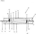
- Film 58 includes a layer of switching material 52 between first substrate 54 and second substrate 56 is electrically connected to electrical connectors 42, 44 via busbars 58a and 58b applied to a conductive coating (not shown) on substrates 54, 56; the conductive coating is in contact with switching material 52. A portion of substrates 54, 56 has been removed to expose the conductive coating where the busbars may be applied.
- First seal 64 is applied in a space 62 between busbar and switching material, adjacent to the cut edge of the switching material. First seal 64 may be in contact with switching material 52.
- First substrate 54 and second substrate 56 are offset along opposing sides 60a and 60b - this provides for access to the conductive surfaces to apply busbars and electrical connectors.
- a generally rectangular-cut film - two sides have aligned edges 57a, 57b.
- a seal may be applied along one or more edges of the switching material.
- a seal may be applied to a perimeter of the switchable layer before or after cutting to a desired size or shape.
- a seal may be applied by dispersing a bead, or applying a strip or die-cut section, of a sealing material along the periphery of the switching material. Other methods of dispersing or applying a sealing material such as extrusion, injection, spraying may also be used.
- the seal may isolate the switching material from other components of the laminated glass or optical filter, or from the ambient environment (e.g. air and/or moisture).
- the die-cut section may be a straight or curved strip, or a continuous shape (polygon, rounded, oval or irregular) to provide a continuous bound to the edge of the switching material.
- First substrate 54 is offset along one edge 90 relative to second substrate 56; second substrate 56 of film 87 is inset along three edges 91, 92, 93, relative to first substrate 54.
- Second substrate 56 of film 87 is inset along three edges 91, 92, 93, relative to first substrate 54.
- Offsetting of some or all edges of the substrate and conductive layer surrounding the switching material in a film, or a portion of the edges, and removal of the switching material along the cut edges provides a busbar mounting platform.
- This offset area may prevent inadvertent electrical contact between the conductive coatings of the first and second substrates which may short out the device, and may provide a larger surface area for the first, second or first and second sealing material to adhere to. Without an offset cut to form a busbar mounting platform, adhesion of a sealing material may be substantively dependent on the through-cut edge of the film - a substantially reduced surface area.
- Figure 4 shows an apparatus non-exemplary to the invention.
- Film 89 has second substrate 56 inset along three edges, relative to substrate 54, with busbar 58a positioned on an offset edge adjacent to that of busbar 58b.
- Electrical connections 42, 44 lead to power source and/or control apparatus from the same corner of film 89.
- Electrical connections 42, 44 may be further embedded in an electrically insulating material (e.g. a seal) to prevent their inadvertent contact with a conductive coating of an opposing substrate.
- a first seal may be placed along the cut edge of the switching material, along the offset.
- a triangular switchable glazing may comprise a triangular film, with two adjacent edges having opposing offsets, with busbars and positioned along the opposing offsets and electrical connectors leading from a common corner of the triangular film.
- a film may be cut to a shape suitable for use in an opthalmic device.
- Film 100 is cut to a general shape suitable for use as, or with, a goggle lens or similar opthalmic device.
- the lens 100 has an arc-shaped upper edge 106 and a lower edge with a cutout section 108 of height X for accommodating a user's nose, between lobed sections to cover the eyes of a user.
- the lens 100 may have a nose bridge section 109 of height Y, with an overall depth of the switchable area (from an upper edge to a bottom edge of the lens, inside the circumferential offset edges) of X +Y.
- the lens may be of unitary construction.
- Film 100 comprises a layer of switching material (not shown) is disposed between first substrate 102 and second substrate 104.
- First and second substrates have interior sides facing each other, and exterior sides facing away. The interior side of one or both substrates has a transparent conductive layer in contact with the layer of switching material.
- First substrate 102 is cut to have a smaller perimeter relative to substrate 104, providing a recessed section along a portion of the perimeter.
- An overhanging tab 110 provides a platform for mounting a busbar 112 on the interior side of substrate 102, in contact with the transparent conductive layer.
- Substrate 104 has a recessed section corresponding overhanging tab 110.
- Busbar 114 is mounted on the interior side of substrate 104, along a portion of an edge of substrate 104, and in contact with a conductive transparent layer on the interior side of substrate 104. Gap 116 separates the cut sections of substrates 102 and 104, providing non-overlapping mounting points for busbars 112, 114. Electrical connectors (not shown) may be mounted to busbars 112, 114 to connect the lens to a source of power to facilitate electrochromic switching of the lens. The offset edges of lens 100 may be sealed using a first and a second sealing material.
- Lens 100 may be shaped to a cylindrical, spherical or frusto-conical configuration, and affixed to a frame using attachment points along a portion of the edge (not shown) or in a frame surrounding the periphery of the lens. Lens 100 may be thermoformed to conform to a spherical, or partially spherical lens shape. Lens 100, once shaped, may be laminated to a static plastic or glass opthalmic device using heat (melt lamination), or a heat or pressure activated adhesive, or combination thereof.
- Substrates 102, 104 may be rigid, or partially flexible plastic that may be formed into a suitable cylindrical, frusto-conical, spherical or partially spherical lens shape, and used in an opthalmic device without a second static glass or plastic lens.
- Decreasing the depth of the nose bridge may generally increase the depth of the cutout section, making the first and second lobes of the lens more pronounced.
- a lens with more or less flexibility about the nose bridge, a flatter profile, or more prominent profile may be formed.
- the ratio of X:Y may be from about 1:10 to about 10:1 or any ratio therebetween, and may be selected according to the desired profile and shape of the lens.
- Y may be any percentage of the depth of the lens X+Y;
- Y may be from about 5% of X+Y to about 95% of X+Y, or any amount therebetween, for example about 10, 15, 20, 25, 30, 35, 40, 45, 50, 55, 60, 65, 70, 75, 80, 85 or 90%, or any amount or range therebetween.
- a lens for a ski goggle may have an X:Y ratio of from about 1:5 to about 1:1, whereas a unitary lens for sunglasses may have a smaller nose bridge, with an X:Y ratio of about 1:1 to about 5:1. It is appreciated however, that any suitable X:Y ratio may be used for ski goggles, sunglasses or any other type of unitary lens, without limitation.
- an electrical potential is applied to the electrodes of the film 100 via busbars 112, 114, and the switching material switches.
- the relationship between the height of the nose bridge Y, and the area of the lens may, in part, impact the speed of the switch of the lens.
- resistivity of the electrode may increase as the nose bridge decreases (Y is reduced and X increased).
- a second pair of busbars 120, 122 may be included ( Figure 5B ), with the electrical potential being applied to both pairs of busbars simultaneously.
- inclusion of first and second pairs of busbars may allow for a faster switch.
- the disclosure further provides, in part, a method for sealing a switchable film, comprising the features as defined in claim 12
- the disclosure non-exemplary to the invention further provides, in part, a method of cutting a switchable film, comprising the steps of providing a switchable film, directing laser radiation at the film to sever a weed portion comprising a portion of a first substrate, but not a second substrate of the switchable film, leaving the conductive layer of the second substrate intact.
- the film comprising a switchable layer may be kiss-cut with a laser.
- the laser is configured to cut only through the upper most substrate and conductive coating, without cutting through or damaging the conductive coating of the lower substrate - the switching material separates the two substrates.
- the penetrative power of the laser when cutting through the upper substrate may be absorbed or dissipated to below a threshold level, and may be further absorbed or dissipated by the layer of switching material.
- the penetrative power of the laser may be a product of the laser power (wattage), the type or source of the laser, whether the laser is a continuous or a pulsed beam, duration of the pulses, and the rate at which the laser is moved across the surface to be cut.
- the laser may be a CO 2 laser; in some embodiments, the laser power may be from about 0.1 to about 5 W or any amount or range therebetween, or from about 0.5 to about 2 W, or any amount or range therebetween; the laser may be pulsed at an interval of from 500 to about 2000 pulses per inch (PPI) or any amount or range therebetween, or from about 1200 to about 1800 PPI or any amount or range therebetween or from about 1400 to about 1600 PPI or any amount or range therebetween; in some embodiments the laser radiation may have a frequency of from about 9 to about 11 microns or any amount or range therebetween. Laser cutting may be performed under a nitrogen blanket.
- PPI pulses per inch
- Pulsing the laser allows application of a substantially consistent amount of energy along a cutline; if insufficient energy is applied to make the cut, the weed portion may not separate cleanly and shorting may result.
- Guidance of the laser may be manual, or may be computer controlled, automated or semi-automated (e.g. CNC automation).
- Kiss-cutting of the film with a laser may be advantageous over cutting with a knife or die - as the active layer of a switchable film may be very thin, any slivers or shards of conductive coating left along the edge after removal of the weed portion of the upper substrate and conductive coating may contact the lower conductive coating and cause an electrical short in the apparatus, and the active layer may fail to switch, or may switch unevenly or slowly.
- the film may be cut in stages. In a first stage, the overall size and shape of the switchable area is defined, and an area of film slightly larger overall cut with flush edges (no offset).
- a first kiss-cut on substrate 54 is made, to provide edge 90. Additional kiss-cuts on substrate 56 may be made to provide edges 91, 92, 93.
- the cuts on substrate 56 may be continuous or separate, and depending on equipment configuration, the film may be turned over afte the first kiss-cut, or a laser cutting head positioned underneath the film may be used. After the film is cut, weed portions are removed, and any switching material remaining on the uncut substrate is removed.
- the one or more cuts may be straight or curved.
- cuts may be at any angle relative to the direction of the web, including parallel, perpendicular or any angle therebetween
- Electrical connectors 58a, 58b may be placed on the conductive coating, for connection of the film to a power source; electrical connectors 42, 44 are also provided.
- the disclosure further provides, in part, a switchable film where the first and the second substrates are in an offset relationship along at least one edge, or along at least two edges.
- the at least two offset edges may be on different substrates, or on the same substrates. Where the at least two offset edges are on the same substrate, they may be adjacent (share a common corner or vertex).
- a portion of a first seal is applied adjacent to the switching material along cut edges 90, 91, 92, 93 - the first seal contacts the cut edge of the switching material and the conductive coating of the uncut substrate. Contact with the uncut surface may aid in maintaining the position of the first seal, to ensure a suitable seal for the switching material.
- support and separation of the substrates and their respective conductive coatings is provided by the switching material itself - a spacer, or the like, is not required to keep the conductive coatings from contacting and shorting.
- the switching material may be cast or extruded as one or more layers on a first substrate, followed by application of the second substrate on top, there is no chamber defined in advance by the substrates and an edge configuration, which may be subsequently filled. Instead, the switching material may be set, cooled or cured to a suitable strength to maintain the separation of the conductive coatings and prevent shorting of the device, even following lamination with heat and pressure. Spacers, beads or other physical devices to maintain separation of the substrates and conductive coating are not needed.
- the film may be produced in advance of knowing the final shape or configuration of the device in which it will be used, and until needed. Suitable shapes - flat or curved (e.g. lenses for helmets, visors, windows of any desired shape) - may later be cut from the film as needed.
- the disclosure further provides, in part, an encapsulated switchable film comprising a layer of switching material between a pair of parallel substrates, and a first and a second conductive coating or layer (first and second electrode) disposed on a first surface of one or both substrates; a first seal surrounding the layer of switching material; first and second transparent layers affixed to a second surface of the substrate; a second seal disposed between the first and second transparent layers, and separated from the switching material by the first seal.
- the switching material may be in contact with both the first and the second electrode.
- the disclosure further provides, in part, a switchable film comprising: a layer of switching material between a pair of parallel substrates, the switching material in contact with a first and a second electrode disposed on a first surface of a substrate; a first seal surrounding the layer of switching material; first and second transparent layers affixed to a second surface of the substrate; a second seal disposed between the first and second transparent layers, and separated from the switching material by the first seal; with the proviso that no spacer is needed to prevent contact of the electrodes.
- the switchable film may be described as a "spacerless" switchable film.
- the disclosure further provides, in part, a method for encapsulating a switchable film comprising: providing a switchable film; comprising a first and a second substrate with a first and second electrode disposed on the surface of at least one of the substrates, and a switching material disposed between the first and second substrates and in contact with the first and second electrodes; disposing a first seal in contact with an electrode and adjacent to the switching material; affixing a transparent layer to the first and second substrates; and disposing a second seal adjacent to the first seal, the second seal separated from the switching material by the first seal.
- a layer of switching material 52 between first 54 and second 56 substrates is electrically connected to electrical connectors 42, 44 via busbars 58a, 58b in contact with a conductive coating (not shown) on substrates 54, 56; the conductive coating is in contact with the switching material 52.
- a portion of substrates 54, 56 has been removed to expose the conductive coating where the busbars may be applied.
- the first seal 64 is applied in a space 62 between the busbar and switching material, adjacent to the cut edge of the switching material. First seal may be in contact with the switching material.
- a second seal 78 may be disposed in a space defined in part by the first and second transparent layers 66, 68 and first seal 64, encapsulating the first seal, busbar and electrical connector.
- the second seal is not contacted by the switching material; this is prevented by the first seal.
- Transparent layers 66, 68 may be affixed to substrates 54, 56 by an adhesive 70.
- the adhesive 70 may be a layer of pressure-sensitive adhesive or a sheet material.
- the adhesive 70 may be pre-cut (die cut, laser cut or other suitable cutting method) to a suitable shape for the switchable film and offset edges, before incorporation into the apparatus.
- the second seal may be a separate application of the same material as the first seal, or may be a different seal.
- the disclosure further provides, in part, a method for encapsulating a switchable film comprising: providing a switchable film; comprising a first and a second substrate with a first and second electrode disposed on the surface of at least one of the substrates, and a switching material disposed between the first and second substrates and in contact with the first and second electrodes; affixing a transparent layer to the first and second substrates; and disposing a first seal in a space defined at least in part by a kiss-cut edge of the switchable film and the transparent layers affixed to the first and second substrates.
- a seal 82 is applied in a space defined in part by the first and second transparent layers 66, 68, and an edge of the switching material 52, filling the space 62 and encapsulating the busbars 58 a, 58b and electrical connectors 42, 44.
- the second seal may comprise a component that interacts with a component in a switching material, creating a detectable change that identifies a deficiency in the first seal - a leak, gap or the like.
- the second seal cures to isolate the switching material from the external environment.
- the first seal may absorb a portion of the switching material, but prevent contact of one or more components of the active layer and second seal long enough for the second seal to complete curing or hardening.
- the uncured or partially cured second seal may contact the switching material. When this occurs, an observable alteration such as a color change may result.
- This observable alteration may be due to an indicator in the switching material, the second seal or both. Detection of a faulty seal early in the manufacture process may allow for defective films or devices to be identified and if appropriate, removed from the production process, to reduce the number of defective devices in the final product lot.
- the indicator of the cured second seal may be activated if the first seal is breached - for example, if the switchable film, or a device comprising the switchable film is twisted or physically damaged. A change in color or other visible indicator draws attention to the damaged device.
- the seal system may comprise one or more indicators for indicating a deficiency in the first seal, the second seal, or both the first seal and the second seal.
- a breach or other deficiency in a seal may result in a product comprising a material that is less durable, or potentially adversely affected by the external environment. Examples of such materials include switchable materials, active layers, suspended particle layers, liquid crystal, photovoltaic materials or the like.
- a switchable material or active layer is exemplified, however any other material adversely affected by a breach in the seal - by ingress of a seal system component or environment interaction (e.g. water, air, oxygen, etc), or by egress of a component of the material (e.g. loss, disruption or inactivation of a component of the material) may benefit from a seal system and/or an indicator system as described herein.
- a schematic diagram of a switchable film with first and second seals is shown generally at 130.
- Active layer 131 is disposed between substrates 132.
- Substrate 132 may include a conductive layer (not shown).
- active layer 131 comprises an indicator material and second seal 134 comprises a trigger material.
- active layer 131 comprises a trigger material and second seal 134 comprises an indicator material. Where first seal 136 fails, interaction of the indicator material and trigger material may be permitted, and a detectable change occurs.
- first seal 136 comprises an indicator material
- a trigger material is a component of the external environment. Where the second seal 134 fails, interaction of the indicator material and trigger material is permitted, and a detectable change occurs.
- Active layer 131 is disposed between substrates 132 and layer 138.
- Substrate 132 may include a conductive layer (not shown).
- active layer 131 comprises an indicator material and substrate 132 comprises a trigger material.
- active layer 131 comprises a trigger material
- substrate 132 comprises an indicator.
- Active layer 131 and substrate 132 are separated by layer 138 - where the integrity of layer 138 fails or otherwise allows contact of substrate 132 with active layer 131, interaction of the indicator material and trigger material is permitted, and a detectable change occurs.
- substrate 132 comprises an indicator material and a trigger material is a component of the external environment. Where substrate 132 fails, or otherwise allows contact of layer 138 with the external environment, interaction of the indicator material and trigger material is permitted and a detectable change occurs.
- active layer 131 may comprise an indicator, and substrate 132 and second seal 134 each comprise a trigger material; the trigger material may be the same or different.
- active layer 131 may comprise a trigger, ad substrate 132 and second seal 134 each comprise an indicator material; the indicator material may be the same or different.
- the first seal 136 and layer 138 may each comprise an indicator material, the indicator material may be the same or different, and the trigger may be a component of the external environment.
- An indicator material or a trigger material may be mixed in, coated on, or dispersed through a seal, substrate, layer or active layer.
- the indicator material or trigger material may be soluble in the seal, substrate, layer or active layer; the indicator material or trigger material may be encapsulated.
- the indicator material is encapsulated and the trigger material disrupts the encapsulating material to release the indicator. Reaction of the indicator material with a component of the seal, substrate, layer or active layer may effect a detectable change.
- the seal, substrate, layer or active layer may comprise a second trigger material to interact with the indicator material to effect the detectable change.
- a detectable change may be a colour change.
- An example of an indicator material may be a dye molecule or dye molecule precursor.
- a dye molecule may undergo a permanent or temporary change from a first colored state to a second colored state.
- a dye molecule precursor may interact with a trigger material and be cleaved, or undergo a chemical reaction (reversible or irreversible) with the trigger material, and change from a first colored state to a second colored state.
- a first colored state and a second colored state may each independently be any color, or may be fluorescent, or may be colourless or substantially colourless.
- the detectable change may be a change in solubility of an indicator material, where contact of the indicator material and trigger material induces precipitation of the indicator material, changing the optical clarity, or light transmittance of the indicator material, or device component (e.g. substrate, layer, seal or active layer)comprising the indicator material.
- the indicator material and trigger material may be encapsulated in layered microcapsules, where the material used for encapsulation maintains the indicator and trigger in separate compartments.
- the material for encapsulation may be solubilized or otherwise disrupted by a component of the active layer e.g. a solvent or plasticizer.
- the encapsulated indicator and trigger materials may be incorporated into the second seal material - when the first seal is compromised, the indicator and trigger are released by interaction with the component of the active layer and a detectable change may be observed.
- Such an embodiment may be advantageous in that no additional materials are added to the active layer, minimizing the complexity of the active layer formulation.
- a redox indicator or an oxidant or reductant as an indicator material in a first or a second seal material may be useful.
- the redox indicator or oxidant or reductant may be incorporated into the second seal material - when the first seal is compromised, the indicator undergoes oxidation or reduction and a detectable change may be observed.
- the indicator material may be encapsulated, and the material used for encapsulation may be solubilized or otherwise disrupted by a component of the active layer.
- the indicator material, trigger material, or both indicator and trigger material may be dispersed in one or more carrier fluids, as a dispersion, suspension or emulsion, or dissolved in a carrier fluid.
- the carrier fluid may be compatible (non-disruptive) of the encapsulating material.
- dyes or dye precursors examples include redox indicators, halochromic indicators, inorganic oxidants or reductants.
- examples of inorganic oxidants or reductants include potassium permanganate and potassium dichromate.
- Redox indicators may be pH dependent, or pH independent.
- halochromic indicators include leuco dyes; some examples of halochromic indicators may include gentian violet (methyl violet 10b) (transition pH range 0.0-2.0), malachite green (first transition pH 0.0-2.0),malachite green (second transition pH 11.6-14),thymol blue (first transition pH1.2-2.8),thymol blue (second transition pH 8.0-9.6),methyl yellow (pH 2.9-4.0),bromophenol blue (pH 3.0-4.6),congo red (pH 3.0-5.0),methyl orange (pH 3.1-4.4),screened methyl orange (first transition pH 0.0-3.2),screened methyl orange (second transition pH 3.2-4.2),bromocresol green (pH 3.8-5.4),methyl red (pH 4.4-6.2),azolitmin (pH 4.5-8.3),bromocresol purple (pH 5.2-6.8),bromothymol blue (pH 6.0-7.6),phenol red (pH 6.4-8.0),neutral red (pH 6.8-8.0),na
- trigger materials include those that may effect a pH change in a local environment (e.g. acids or bases); a pH change may trigger a color change in a halochromic indicator.
- trigger materials include propionic acid, butyric acid, valeric acid, caproic acid, caprylic acid, capric acid, lauric acid, myristic acid, palmitic acid, stearic acid, cyclohexanoic acid, phenylacetic acid, benzoic acid, toluic acid, chlorobenzoic acid, bromobenzoic acid, nitrobenzoic acid, phthalic acid, isophthalic acid, terephthalic acid, salicylic acid, hydroxybenzoic acid and aminobenzoic acid, or the like.
- Examples of materials that may be used to encapsulate indicator materials or trigger materials include Acrylonitrile-Butadiene-Styrene Copolymer , Acrylonitrile-Methyl acrylate copolymer, acylonitrile-styrene-acrylate copolymer, amorphous nylon, arabinogalacatan, beeswax, carboxymethylcellulose, carnauba, cellulose, cellulose acetate phthalate, cellulose nitrate, cyclic olefin copolymer, epoxy resin, ethylcellulose, ethylene , ethylene-chlorotrifluoroethylene copolymer , ethylene-tetrafluoroethylene copolymer, ethylene-vinyl acetate copolymer, ethylene-vinyl alcohol copolymer, fluorinated ethylene-propylene copolymer, stearyl alcohol, gelatin, glyceryl stearate, glycol modified polycyclohe
- a trigger material of an external environment may include a material that 'poisons' the switching action of the active material.
- a material that injects or scavenges electrons may disrupt the reductive or oxidative switch - slowing it down or stopping it altogether.
- disruption of the movement of the ionic species may disrupt the switch - slowing it down or stopping it altogether.
- the poison may disrupt polymerization of a switching material - preventing it from completing, or inducing undesirable polymerization.
- the trigger material from the external environment may include ambient air, or a gas, or a component thereof, e.g. carbon dioxide, oxygen, H 2 S, water, or other material in the environment external to the active layer.
- indicator materials that undergo a detectable change with exposure to water include cobalt (II) chloride, copper (II) sulfate.
- the indicator material may be incorporated in a first seal, when the second seal is compromised, water, water vapor or air from the external environment may interact with the indicator material to induce a detectable colour change.
- the indicator material may be responsive to oxygen, and oxygen may be a trigger material.
- the indicator material may be included in the first seal, and if the second seal is compromised, oxygen in the external environment may interact with the indicator material to provide a detectable change.
- US 8647876 discloses several indicator materials that may undergo a colour change, or become chemiluminescent, when exposed to oxygen.
- a first seal may comprise an indicator material and a trigger material may be encapsulated in a layered microcapsule, and the encapsulating material may be water soluble.
- the second seal is compromised, water or water vapor from the external environment may disrupt the encapsulation, allowing interaction of the indicator and trigger, providing a detectable change.
- water soluble encapsulating materials may include gelatin, gum arabic, starch, polyvinylpyrrolidone, carboxymethylcellulose, hydroxyethylcellulose, methylcellulose, arabinogalacan, polyvinyl alcohol, polyacrylic acid, or a combination thereof, or the like.
- the switching material may include an indicator material; the indicator material may be a diarylethene, and the second seal may include a trigger material; the second seal may be a two-part epoxy, such as that described in US 6248204 , and the trigger material may be an epoxy resin an epoxy resin hardener or both an epoxy resin and an epoxy resin hardener.
- a switchable film may be further laminated with heat and pressure between layers of glass, to provide a switchable, laminated glazing.
- the disclosure further provides, in part, a laminated glass comprising: a switchable film; an electrical connector for electrically connecting the first and the second electrodes to a power source; and a first seal contacting an edge of the layer of switching material.
- the switchable film may be an encapsulated switchable film.
- the switchable film may be layered between layers of PVB, and this between first and second layers of glass.
- the glass-PVB-switchable film-PVB-glass sandwich may be passed through a press roll, pressed between plates at an elevated temperature (about 90°C to about 140°C - pressure and temperature may be increased and decreased over several steps), or may be placed in a vacuum bag (rubber), with an initial bonding at a temperature of about 70°C-110°C, while applying a vacuum to remove air between the layers.
- a second bonding step may then be performed at a temperature of about 120°C-150°C, with pressure (e.g. about 0.95 MPa to about 1.5 MPa in an autoclave).
- the overall thickness of the laminated glass is dependent, in part on the thickness of the various layers.
- Laminated glass may have advantages for strength, safety, impact resistance, reduction in noise or the like), and inclusion of a switchable compound provides additional, advantageous features over conventional laminated glass.
- a switchable film is "laminatable” if it retains the ability to fade and darken after lamination.
- a seal for a switchable film or used in a device comprising a switchable film prevents ingress of matter that may affect performance of the switching material.
- a switching material is self-supporting, support or separation devices such as spacers, beads, dividers or the like are not needed in the seal.
- the switching material is part of a film that is to be laminated between rigid substrates (e.g. using heat and pressure such as for a laminated glass), it may be advantageous to use seals that are compressible, to prevent breakage of the glass during lamination.
- Seals may be a thermoplastic, a thermoset, a rubber, a polymer or metal, a metallized tape, or combinations thereof.
- a seal may be selected to provide good adhesion to contacted surfaces (substrate, conductive layer, electrode, switching material, electrical connectors or the like, and to provide sufficient flexibility, barrier properties, mechanical durability and adhesion at the operating temperature of the switchable layer to maintain the isolation of the switching material - for example, a seal may be selected that does not crack or crumble, break down, or lose adhesion as the temperature changes.
- a seal may not interact with the switching material, or "poison" or interfere with the photochemistry and electrochemical performance of the switching material.
- a seal may be electrically insulating.
- a seal may be gas-impermeable.
- a seal may be resistant to water, or may be water impermeable.
- a seal may comprise a dessicant to scavenge any residual water that may be present.
- dessicants include zeolites, activated alumina, silica gel, calcium sulfate, calcium chloride, calcium bromide and lithium chloride, alkaline earth oxide, potassium carbonate, copper sulfate, zinc chloride or zinc bromide.
- a dessicant may be dispersed in a seal, or applied to a surface of a seal.
- Thermoset materials include polymers, rubbers and plastics.
- thermoset seals include polymers with reactive groups.
- polymers may include silicones and siloxanes.
- reactive groups include vinyl groups, hydride groups, silanol groups, alkoxy or alkoxide groups, amine groups, epoxy groups, carbinol (polyester or polyurethane groups), methacrylate or acrylate groups, mercapto (thiol, polythiol groups), acetoxy, chlorine or dimethylamine groups. Curing or hardening of such materials may be chemical, radiation, temperature or moisture dependent.
- Examples of radiation curing may include exposure to light (UV light or visible light); examples of temperature curing may include resting the material at an elevated temperature; examples of chemical curing may include a condensation reaction, an addition reaction, vulcanization, or the like.
- the chemical curing may include a catalyst, or addition of a reactive group to facilitate crosslinking of a polymer. The chemical cure may further be heated to accelerate the curing reaction, or may be cooled to retard the curing reaction.
- vinyl functional polymers may be employed in an addition cure system (e.g. Pt catalyzed); hydride functional polymers may be employed in an addition cure system; siloxane functional polymers may be employed in a condensation cure system (e.g. silicones with one part or two part room temperature vulcanization (RTV)), or an acetoxy, enoxy, oxime, alkoxy or amine moisture-cure system.
- addition cure system e.g. Pt catalyzed
- hydride functional polymers may be employed in an addition cure system
- siloxane functional polymers may be employed in a condensation cure system (e.g. silicones with one part or two part room temperature vulcanization (RTV)), or an acetoxy, enoxy, oxime, alkoxy or amine moisture-cure system.
- RTV room temperature vulcanization
- Thermoplastic materials may include polymers, rubbers and plastics that melt or flow at elevated temperatures, and reversibly set to a non-flowing state at a reduced temperature.
- thermoplastic materials include poly(vinyl alcohol), poly(vinylidene chloride), polyvinylidene fluoride, ethylene vinyl acetate (EVA), and polyvinyl butyral (PVB),
- rubbers include polyisoprene, polyisobutylene (PIB), poly(isobutylene-co-isoprene), block, copolymer and graft polymer of butadiene-styrene, poly(chlorobutadiene), poly(butadiene-co-acrylonitrile), poly(isobutylene-co-butadiene), acrylate-ethylene containing copolymer rubber, poly(ethylene-co-propylene), poly(ethylene-co-butene), ethylene-propylene-styrene copolymer rubber, poly(s
- a seal overlaid with a metal layer or metal foil or tape may be a useful edge seal system.
- epoxy seal materials include DP100, DP105, DP110, DP125 from 3M; 1C, E-30-CL, M-31 CL from Hysol; EP415S-1HT from MasterBond, Delo LP655.
- silicone seal materials include Sylgard182, RTV3165, RTV791, RTV9-1363, RTV948 from Dow; or SWS, SCS2000, RTV102, RTV6700 or RTV11 from Momentive, RGS7730, HM2500, CAF520 (Blustar); PV8303, RTV791, RTV730, RTV795 from Dow; SCS2000 from Momentive.
- polyurethane seal materials include Titebond MP75 HiPURformer, 3M Scotch-Weld DP605 NS, Lord 6650, Hysol U09FL, Examples of acrylic seal materials include Tremflex 834, 3M 8211, 3M 8172PCL, Surlyn 1601, Surlyn 1703. Examples of ethyl vinyl acetate seal material include EVASAFE (Bridgestone), 3M Scotch-Weld 3764, 3M Scotch-Weld 3792. Examples of olefin polymer (polyolefin) seal materials include 3M Scotch-Weld 3748. Examples of polysulfide seals include THIOKOL. Examples of polyethylene seal materials include silane-crosslinked polyethylene (Solvay).
- isobutylene rubber seal materials include OppanolB15, OppanolB50, OppanolB12, OppanolB10 from BASF, Tremco 440, HL-5140 (HB Fuller), Poly(isobutylene-co-isoprene) from Scientific Polymer.
- Some isobutylene seal materials comprise polyisobutene (polyisobutylene).
- Some ethyl vinyl acetate seal materials may comprise ethylene-vinyl acetate polymer (55-75$ by weight and hydrocarbon resin (25-45 % by weight). Some ethyl vinyl acetate seal materials may comprise ethylene-vinyl acetate polymer (50-65% by weight), hydrocarbon resin (25-35 % by weight), polyethylene polymer (5-10 % by weight), polyolefin wax 91-5% by weight) and an antioxidant (0.5-1.5 % by weight).
- Some polyolefin polymer seal materials may comprise polypropylene (15-40 % by weight), hydrocarbon resin (10-30 % by weight), styrene-butadiene polymer (10-30 % by weight), ethylene-propylene polymer (5-25 % by weight), polyethylene (5-20% by weight) and polyolefin wax (7-13% by weight).
- the seal may swell; swelling may occur during curing (for seals that are cured), or may swell after installation by absorption of a component of the switching material. For some embodiments, this may be advantageous in instilling the sealing material into small gaps or separations.
- Sealing materials may be tested by immersion of a sample in a solvent and observed periodically for swelling, loss of mass, degradation, crumbling or other indicator of interaction with the solvent or components dissolved in the solvent. In some embodiments, some degree of swelling may be advantageous in a sealing material, in that the sealing material may expand to fill any gaps or spaces after installation. Sealing materials may also be tested by sealing a layer of switching material between substrates in a device. Devices with a single seal may be weighed (determine initial mass) and placed in an oven, and periodically weighed to assess any loss in mass - a loss in mass may be indicative of a sealing material that is not impermeable to the solvent or plasticizer or other component of the switching material.
- Devices may be further examined for the initial and ability to photochemically and/or electrochemically transition the switching material from a dark state to a faded state, or from a faded state to a dark state.
- the devices may be inspected for visual defects - uneven switching, development of spots, bubbles or other defects, or the like.
- first seals may include: silicones (e.g. Sylgard182, RTV3165, RTV791, RTV9-1363, RTV948 from Dow; or SWS, SCS2000, RTV102 or RTV11 from Momentive), or isobutylene rubbers (e.g. polyisobutylene).
- silicones e.g. Sylgard182, RTV3165, RTV791, RTV9-1363, RTV948 from Dow; or SWS, SCS2000, RTV102 or RTV11 from Momentive
- isobutylene rubbers e.g. polyisobutylene
- first seals may include: silicones (e.g. RGS7730, HM2500, CAF520 (Blustar); PV8303, RTV791, RTV730, RTV795 from Dow; SCS2000 from Momentive), some epoxies (e.g. DP110 from 3M), polyisobutylene rubbers (e.g. OppanolB15, OppanolB50, OppanolB12, OppanolB10 from BASF), or polysulfides.
- silicones e.g. RGS7730, HM2500, CAF520 (Blustar); PV8303, RTV791, RTV730, RTV795 from Dow; SCS2000 from Momentive
- epoxies e.g. DP110 from 3M
- polyisobutylene rubbers e.g. OppanolB15, OppanolB50, OppanolB12, OppanolB10 from BASF
- first seals may include: silicones (e.g. Sylgard 182, RTV791 from Dow; RTV102, RTV106, RTV6700, SCS2000 from Momentive; SCS9000, RTV100); polyisobutylene rubbers (e.g. OppanolB15, OppanolB50, OppanolB12, OppanolB10 from BASF); poly(isobutylene-co-isoprene rubber).
- silicones e.g. Sylgard 182, RTV791 from Dow
- RTV102, RTV106, RTV6700, SCS2000 from Momentive SCS9000, RTV100
- polyisobutylene rubbers e.g. OppanolB15, OppanolB50, OppanolB12, OppanolB10 from BASF
- first seals may include: silicones (e.g. Sylgard 182, RTV791 from Dow; RTV102, RTV106, RTV6700, SCS2000 from Momentive), polyisobutylene rubbers (e.g. OppanolB15, OppanolB50, OppanolB12, OppanolB10 from BASF).
- silicones e.g. Sylgard 182, RTV791 from Dow
- polyisobutylene rubbers e.g. OppanolB15, OppanolB50, OppanolB12, OppanolB10 from BASF.
- first seals may include: epoxies, silicones (e.g. Sylgard 182, RTV791, RTV730 from Dow; SCS2000, RTV6700 from Momentive), or polyisobutylene rubbers (e.g. OppanolB15 from BASF).
- silicones e.g. Sylgard 182, RTV791, RTV730 from Dow; SCS2000, RTV6700 from Momentive
- polyisobutylene rubbers e.g. OppanolB15 from BASF.
- the first seal may be a temporary barrier, separating the switching material from a second seal.
- the first seal may swell or absorb plasticizer or other component from the switching material (in a sufficiently small amount so as to not detrimentally affect the operation of the switching material).
- the first seal may also be unreactive with the second seal.
- the second seal may be reactive with the switching material in an uncured, but not a cured state.
- the second seal may be sufficiently fast curing so as to complete the curing process before components of the switching material swell and migrate through the first seal. Selection of such a combination of first and second seal materials may be counter-intuitive based on initial testing results, but when combined, provide an improved seal system. Examples of such seal systems may include a PIB first seal material, and an epoxy or EVA second seal material.
- the first seal material may be substantially non-reactive with the switching material and the second seal material; the second seal material may be reactive with the switching material (e.g. swelling, softening or the like).
- the second seal material may, on the other hand be preferable for resistance to environmental aspects - it may be particularly durable, or resistant to oxygen or water, for example. Selection of such a second seal material may be counter-intuitive based on initial testing results, but when combined with a suitable first seal material, an improved seal system is realized.
- Active layer an active layer comprises a switching material.
- An active layer as referenced herein may include any solid, semi-solid, gel or liquid material that alters light transmittance in response to a stimulus.
- An alteration in light transmittance may be a change in one or more of transparency, opacity, color, haze; the reduction in light transmittance may be selective - the a portion of UV, visible or IR light that is transmitted by the active layer may change, or selective wavelengths be blocked, at least in part.
- the stimulus may include one or more than one of electricity (an electrochromic active layer), temperature or temperature change (a thermochromic active layer), electromagnetic radiation in a range of from about 300 nm to about 750 nm or any amount or range therebetween (UV or visible light) (a photochromic active layer).
- an electrochromic active layer temperature or temperature change
- thermochromic active layer electromagnetic radiation in a range of from about 300 nm to about 750 nm or any amount or range therebetween (UV or visible light)
- Some active layers may be responsive to both light and electricity (a photochromic-electrochromic active layer).
- Some active layers comprise a polymer or polymer matrix and one or more compounds or compositions that undergo a structural change or orientation in response to the stimulus.
- a liquid crystal or suspended particle display electrochromic active layer comprises discrete particles suspended in a liquid or semi-solid polymer matrix, and the alignment of the crystals or particles is controlled by application of electricity.
- Other examples of electrochromic active layers comprise two or more compounds that behave as a redox pair - when electricity is applied, one compound is electrochemically oxidized to a coloured state, and the other is electrochemically reduced to a coloured state. When electricity is removed, the compounds revert to their uncoloured state.
- Some photochromic materials when exposed to UV light, change color - darken or fade. Some photochromic materials may have 'memory' in that they remain in the UV-exposed state until a second stimulus is applied; others do not exhibit memory, and will gradually revert to their unexposed state.
- Some active layers comprise materials that are both photochromic and electrochromic. When exposed to selected wavelengths of light (e.g. UV light), the materials darken. When exposed to electricity, the materials fade.
- Examples of compounds (chromophores) that may be useful in a photochromic-electrochromic active layer include some switchable compounds such as photochromic-electrochromic diarylethenes (see, for example US 7777055 , WO2010/142019 and WO2013/044371 ).
- An active layer comprising one or more of these compounds may be transitionable from a faded state to a dark state with exposure to UV light, and from a dark state to a faded state with application of electricity, or light in the visible range.
- a switching material may comprise a polymer and a switchable compound, and optionally, one or more of a plasticizer, dye, UV light stabilizer, antioxidant, supporting electrolyte, surfactant, adhesion promoter or adhesion control agent or the like.
- the switching material may comprise part of an active layer.
- the switching material may be a single layer of material (cast or extruded), or maybe two or more layers, cast or extruded sequentially or simultaneously one on top of the other. Generally, the switching material is substantially optically clear, or with minimal (e.g. less than 3%) haze.
- the switching material may comprise adhesive properties.
- a switching material may be described as "laminatable” if it retains the ability to fade and darken after lamination (e.g. after elevated temperature and/or pressures used during a glass lamination process). Haze may be measured using methods known in the art, for example use of an XL-211 Hazemeter from BYK-Gardner.
- Components of the switching material may further provide, in part, one or more than one secondary functions.
- any of a switchable compound, polymer, plasticizer, supporting electrolyte, charge carrier or the like may provide a secondary function as one or more than one of a plasticizer (solvent), polymer, supporting electrolyte, or the like.
- the polymer may provide multiple functionalities, including a combination of polymer and switchable compound, and in some embodiments, a charge carrier function, a plasticizer function and/or a supporting electrolyte function. Inclusion of different switchable compounds and/or different polymer backbone moieties may alter the function of the polymer.
- solvents which may function as plasticizers in the switching material
- solvents include dimethyl adipate, diethyl adipate, 2-(2-butyoxyethoxy) ethyl acetate, triglyme, diethyl succinate, 2,2,4-trimethyl-1,3-pentanediol monoisobutyrate, dimethyl-2-methyl glutarate, butylene carbonate, dibutyl itaconate, tetraethylene glycol di-heptanoate, triethylene glycol di-2-ethylhexanoate, triethylene glycol di-2-ethyl butyrate, triethylene glycol di-n-heptanoate, benzyl octyl adipate, di-n-hexyl adipate, triethylene glycol, combinations thereof, or the like.
- Examples of supporting electrolytes include tetrabutylammonium tetrafluoroborate (TBABF 4 ), tetrabutylammonium bis((trifluoromethyl)sulfonyl)imide (TBATFSI).
- TABF 4 tetrabutylammonium tetrafluoroborate
- TATFSI tetrabutylammonium bis((trifluoromethyl)sulfonyl)imide
- polymers examples include ethylene copolymers (e.g. ethylene-vinyl acetate,), apolyurethane, a polyalcohol, an ionomer, PVDF, or the like.
- polyalcohols include ethylene vinyl alcohol copolymer, polyvinyl alcohol, polyvinyl acetals (e.g. polyvinyl butyral - PVB), poly(ethylene oxide), or the like.
- ionomers examples include poly(ethylene-co-methacrylic acid, PV5300 (DuPont) or the like.
- the switching material may comprise a mixture of polymers. Other polymers having a suitable glass transition temperature may also be used.
- a polymer may be crosslinked.
- a crosslinking agent may comprise two or more reactive groups; reactive groups may independently be, for example, aldehyde, epoxide, isocyanate, silane or the like.
- aldehyde crosslinkers include terephthalaldehyde and the like.
- epoxides include diglycidyl ethers of polypropylene glycol (e.g.
- isocyanate crosslinking agents include hexamethylene diisocyanate (HMDI), dimers, trimmers, or multimers of HMDI (e.g. DESMODUR TM N100, N3300A, N3600 from Bayer) and the like.
- HMDI hexamethylene diisocyanate
- dimers, trimmers, or multimers of HMDI e.g. DESMODUR TM N100, N3300A, N3600 from Bayer
- the one or more supporting electrolytes may be absent, or present in an amount of from about 0.1% to about 20% (by weight) or any amount or range therebetween, for example 1, 2, 3, 4, 5, 6, 7, 8, 9, 10, 11, 12, 13, 14, 15, 16, 17, 18 or 19%.
- the one or more plasticizers (solvents) may be absent, or may be present in a switching material in an amount ranging from about 5 wt% to about 90 wt% or any amount or range therebetween.
- the one or more switchable compounds may be present in a switching material in an amount (% weight) of from about 0.05% to about 80%, or any amount or range therebetween, for example about 5, 10, 15, 20, 25, 30, 35, 40, 45, 50, 55, 60, 65, 70 or 75%.
- the polymer may be present in an amount of from about 10 wt% to about 95 wt%, or any amount or range therebetween, for example 15, 20, 30, 40, 50, 60, 70, 80 or 90 wt%.
- the one or more transparent, or substantially transparent, substrates may be glass - float glass, tempered glass, toughened, or chemically -strengthened glass, an organic glass or the like.
- the substrate may be flexible (e.g. plastic film, glass film, or glass microsheet).
- An organic glass is an amorphous, solid glasslike material made of transparent plastic.
- Organic glass may provide advantages such as toughness, reduced weight, improved thermal insulation, ease of colour modification (incorporation of colorants in the plastic when molding) or the like.
- organic glasses or plastics examples include polycarbonate, acrylonitrile butadiene styrene, polyesters (polyethylene terephthalate (PET), modified PET), acrylics (polymethyl methacrylate) or modified acrylics (e.g.
- polyester carbonate polyethylene carbonate
- allyl diglycol carbonate polyether imide
- polyether sulfone polysulfone, PSU
- cellulose acetate cellulose butyrate
- cellulose propionate polymethyl pentene
- polyolefins nylon
- polyphenylsulfone polyarylate
- polystyrene polycarbonate
- polysulfone polyurethane
- polyvinyl chloride polystyrene acrylonitrile
- ethylene vinyl acetates or the like.
- one or more of the components of the switching material may be selected to be immiscible, or insoluble, with one or more of the components of the organic glass, to prevent diffusion into the glass.
- a solvent or plasticizer used in some embodiments described herein may be immiscible, or insoluble, with a plasticizer used in an organic glass.
- Combinations of organic glass and switching material materials with one or more immiscible components may be selected in this way.
- a layer of plastic e.g. PET film
- Substrates may independently be of any suitable thickness.
- Substrates may independently be coated with, or comprise anti-scratch layers, security films, heat or infrared reflecting or absorbing materials, or UV reflecting or absorbing materials or the like.
- Glass layers may independently be tinted; examples of tinted glass include grey, bronze or green glass, or may comprise coatings or additives to block some wavelengths of light (e.g. portions of UV, VIS, IR incident light or the like).
- Glass layers may be tinted. Color and depth of coloration of tinted glass may be selected to achieve certain levels of light transmission (visible, UV or IR), or to harmonize with the site of installation e.g. exterior automotive paint, building envelope, or to harmonize with other components of a laminated glass. Glass color may be described with reference to colour values L ⁇ a ⁇ and b ⁇ , and/or light transmittance (LT A ). As examples, US 5308805 describes a neutral low transmittance glass and US 7932198 describes examples of grey glass.
- a substrate may be clear, or may be grey, with an LT A of about 25-35% or any amount or range therebetween.
- a second substrate may be clear, or may be colored (e.g. grey), with an LT A of about 75-85% or any amount or range therebetween.
- a substrate may be glass or plastic (an "organic glass").
- a substrate may be flexible or rigid.
- a substrate may be coloured to harmonize with the exterior paint of the vehicle or building where the laminated glass is installed, or to mask the inherent color of one or more layers in the laminated glass (e.g. the active layer, the static filter or the incident light filter, for embodiments where one or more of these layers has a colour that does not harmonize with the surrounding surface or paint).
- a substrate may be substantially clear to allow as much light as possible reach the active layer.
- the glass is an organic glass
- a layer of plastic e.g. PET film
- an adhesive layer or sound insulating layer comprising PVB to prevent diffusion of plasticizers or other components of the adhesive layer into the organic glass.
- the substrate may be of uniform or varying thickness, and of any suitable dimension.
- the substrate may have a thickness from about 0.01 mm to about 10 mm, or any amount or range therebetween, for example 0.05, 0.1, 0.5, 1, 2, 3, 4, 5, 6, 7, 8, 9 or 10 mm, or from about 0.012 mm to about 10 mm, or from about 0.5 mm to 10 mm, or from about 1 mm to 5 mm, or from about 0.024 mm to about 0.6 mm, or from about 0.051 mm (2 mil) to about 0.178 mm (7 mil).
- the thickness and/or material of a first substrate differs from the thickness and/or material of a second substrate.
- Conductive coatings may be transparent.
- a conductive coating may include a transparent conducting oxide (TCO) such as indium tin oxide (ITO), fluorine tin oxide (FTO) or the like, metal or metal oxide coatings (e.g. silver, gold or the like), transparent conducting polymers, or other substantially transparent conductive coatings.
- TCO transparent conducting oxide
- ITO indium tin oxide
- FTO fluorine tin oxide
- metal or metal oxide coatings e.g. silver, gold or the like
- transparent conducting polymers e.g. silver, gold or the like
- transparent conducting polymers e.g.
- transparent substrates with conductive coatings include ITO-coated glass, or FTO-coated glass (e.g. TEC glass from Pilkington).
- the electrode pattern e.g. interdigitated electrodes such as that illustrated in Figure 3c
- a substrate with a conductive layer may be ITO-coated glass, or ITO-coated PET.
- a conductive coating
- Some methods of manufacture of conductive coatings may necessitate use of selected substrates that tolerate the coating methods.
- FTO coatings may be less expensive, and thus an attractive substrate and conductive coating, but require a substrate that tolerates the high temperatures (>400°C) used in some coating methods.
- Glass may be suitable for this application, however some plastics or films may not. Having a switchable switching material that may be laminated between FTO-coated substrate may provide a less expensive laminated glass.
- both first and second electrodes may be disposed on one substrate.
- First and second coplanar electrodes may be etched into the conductive coating or printed on the surface of the substrate in a suitable pattern e.g., a discontinuous conductive coating providing first and second electrodes on the same substrate.
- a second substrate may lack a conductive coating, and first and second busbars and electrical connectors may be disposed on the first and second electrodes of the first substrate.
- the second substrate (lacking a conductive coating) may be a plastic or glass, or a film or release liner.
- PCT publication WO2012/079159 describes coplanar electrode configurations that may be useful in some embodiments.
- components of the switching material may be combined in subcombinations ('parts'), with the parts combined at a later step.
- Preparation of a switching material in one or more parts may be advantageous to solubilize one or more components of a switching material, prevent side reactions, or to prevent initiation of crosslinking ('curing') before the formulation is complete or ready for casting or coating.
- a switching material may be prepared according to the following steps: providing a first part comprising a polymer, a switching compound, a salt and a first portion of a solvent; providing a second part comprising one or more crosslinking reagents and a second portion of the solvent; providing an accelerant and an optional co-solvent; combining the first part and the second part; and combining the third part with the combined first and second parts.
- the switching material may be coatable.
- a coatable switching material is one that is of suitable viscosity to be applied to a substrate in a suitable thickness and substantially uniform manner. Viscosity of a switching material may be altered by increasing or decreasing the quantity of sacrificial solvent, altering the polymer (different quantity and/or molecular mass), increasing or decreasing temperature of the switching material, inclusion of a rheology modifier or the like. In some embodiments, the switching material does not include a sacrificial solvent, and viscosity is manipulated by heating the switching material and/or using a heated die for coating.
- Partial curing of the switching material in advance of, or during the process of coating may also increase the viscosity of the switching material applied to a moving web, or extruded or injected into a mold or extruded or applied onto a substrate. Curing may be slowed or stopped by decreasing temperature, and/or diluting the partially cured material with a co-solvent. Increasing temperature and/or removal of the co-solvent may subsequently allow curing to proceed to completion.
- a switching material, or one or more parts thereof may be treated to remove dissolved gas (oxygen, air, or the like), and/or treated to remove water, or prepared in an environment with reduced oxygen and/or reduced humidity.
- one or more of the steps of making a switchable formulation, coating a substrate, and/or curing the film may be performed in an inert atmosphere (e.g. nitrogen, with less than 100 ppm oxygen, less than 100 ppm water, or both); a reduced humidity atmosphere (e.g. about 5-15% relative humidity), or in an open atmosphere.
- a method of making a coatable formulation, coating of substrates and/or curing of a switching material may be performed in a reduced humidity and/or reduced oxygen environment, for example less than 100 ppm relative humidity, and/or less than 100 ppm oxygen.
- a switching material may be coated at a suitable thickness onto a conductive coating of a substrate using a slot die, knife coater, roll-to-roll coating method, extrusion, dipping, spraying, spin coating, gravure coating method, hand-drawing or the like.
- a suitable coating thickness may be selected such that the switching material is of the desired thickness once the co-solvent is evaporated (if a co-solvent is present), or the final layer is of the desired thickness following cooling and/or crosslinking of the coated switching material. For example, to obtain a final thickness of about 50 microns, a switching material with co-solvent may be applied to the substrate in a layer of about 100 to about 120 microns.
- a second layer of substrate is laminated on top of the coated switching material (conductive side in contact with the switching material) to form a sandwich structure.
- the ' sandwich' may be cured, or allowed to continue to cure (if curing is initiated during the coating or laminating process) and if desired, cut to a suitable size. Busbars or other electrical contacts may be added if desired.
- a second substrate may be applied on top of the disposed switching material; the second substrate may comprise a conductive layer, positioned so as to be in contact with the switching material.
- the resulting film may be cut to a desired size or shape. Electrical contacts (e.g. busbars, wires or the like) may be added, to facilitate application of a voltage to the switching material.
- the switching material may be cured or crosslinked before, or after application of the second substrate.
- the step of curing may comprise heating the switching material to a temperature suitable for crosslinking (e.g. about 20°C to about 90°C, or any amount or range therebetween.
- the step of disposing may be preceded by a step of filtration of the switching material.
- a switching material may be formed into pellets, chips or flakes and mixed with other components(e.g. in a screw mixer) and extruded through a die to form one or more layers or films.
- the mixer, die and/or extruder may be heated.
- the extruded material may itself be pelletized, for subsequent blending with other materials and extruded in a second extruder to produce a switchable film, or molded to produce a switchable article.
- One or more additional components may be imbibed or soaked into the cast layer. If the switching material is to be crosslinked, this may be done before or after removal of sacrificial solvent (if used).
- the switching material may be configured to include spaced projections defining a surface irregularity (a "rough texture") - if such a switching material is laminated with heat and pressure between rigid substrates, the surface irregularity may facilitate removal of air from during the lamination process, and/or to facilitate handling of the unlaminated switching material.
- a surface irregularity a "rough texture"
- two or more layers of switching material may be coextruded, or a first layer (e.g. comprising the switchable compound as a monomer, or as part of a switchable polymer) may be applied (coated) onto the second layer.
- a release liner may be used for support in handling, and/or separation of layers when rolled for storage and handling.
- the first layer, or a component thereof may remain as a discrete layer, or may diffuse into the second layer to create a gradient, or may be imbibed into the second layer to provide a substantially uniform distribution, or a gradient distribution, of switchable compound within the second layer.
- the gradient may comprise a region of higher concentration along one surface of the second layer, and a region of lower concentration extending through the plane of the second layer. In other embodiments, the gradient may be established so as to extend along the plane of the second layer.
- a first layer may be applied to a first substrate, and a second layer applied to a second substrate (e.g. disposed on a conductive coating on the surface), and the substrates arranged to place the first and second layers adjacent, and the substrate-switching material-substrate sandwich laminated.
- the first layer may be applied to the second layer, or to a substrate by any of several methods, for example electrodeposition, vapor deposition, chemical deposition, chemical plating, brushing, spraying, extruding, slot-die coating, dipping or the like, or a combination thereof. If a co-solvent is used, it may be removed by evaporation. Where it is desired to vary the color or color density of the switching material, the switching compound may be applied using printing methods that deposit droplets of varying size and/or spacing - for example, smaller, and/or more widely spaced dots yield regions of lesser switching material, while larger, and/or more closely spaced dots yield regions of greater switching material.
- a layer of switchable compound may be imbibed into a surface of the polymer, or may be applied as a layer of liquid and dried to a solid or semi-solid, or may be a solid or semi-solid of any suitable thickness; a suitable thickness may be selected dependent on the concentration of the switchable compound and the desired deposition amount.
- the layer of switchable compound is of uniform, or substantially uniform, thickness.
- the layer of switchable compound is of non-uniform thickness.
- the switchable compound may be in a crystallized form, or may be amorphous, or a combination thereof.
- Busbars may be applied to a portion of the conductive layer or electrodes so that a voltage differential is created across the layer (s) comprising the switchable material to effect the switch.
- the busbars may be of any suitable material to provide a low-profile conductive area suitable for attachment of an electrical connector thereto. Examples of suitable materials include conductive adhesive, conductive ink, conductive epoxy, conductive tape, metal mesh or film or the like, comprising at least one type of conducting material for example a metal, such as aluminum, gold, silver, copper or the like.
- the conductive material may be applied to the conductive surface by any of several methods known in the art, including printing, painting, screenprinting ('silkscreening'), stenciling (stencil printing) or the like.
- Electrical connectors or leads may be of any suitable material and may be affixed to the busbar by any suitable methods, including adhesion (conductive adhesive or conductive epoxy), soldering, clips, rivets or the like.
- Suitable material for electrical connectors may include conductive tape, wire, copper tape, copper-clad polyimide film (e.g. Kapton) or the like.
- the electrical connector may be doubled-sided.
- a control circuit can be used to switch the electrical voltage on or off, based on input from an automated or semi-automated device (e.g. an irradiance meter, thermometer), a building or vehicle environmental control system, a user or some other input, and can also be used to modulate the voltage to a predetermined level.
- a power source may include an AC line voltage in a house or other building, a DC power source (e.g. a battery of a vehicle, or in a separate battery or power pack), an energy harvesting power source (e.g. solar panel) or the like.
- the control circuit may comprise one or more switches (transistor, relay, or electromechanical switch) for opening and closing a circuit between the voltage regulators and conductive layers of a substrate, an AC-DC and/or a DC-DC converter for converting the voltage from the power source to an appropriate voltage; the control circuit may comprise a DC-DC regulator for regulation of the voltage.
- the control circuit can also comprise a timer and/or other circuitry elements for applying electric voltage for a fixed period of time following the receipt of input.
- Embodiments include switches that can be activated manually or automatically in response to predetermined conditions, or with a timer.
- control electronics may process information such as time of day, ambient light levels detected using a light sensor, user input, stored user preferences, occupancy levels detected using a motion sensor, or the like, or a combination thereof, the control electronics configured to activate switches for applying voltage in response to processed information in accordance with predetermined rules or conditions.
- the power control electronics comprises a user-activated switch.
- a user-activated switch may be a 'normally-open', or 'normally-closed' switch, for example a push-button switch.
- a switch may be configured to remain closed for a predetermined amount of time following actuation, thereby facilitating application of voltage for sufficient time to effect a state transition.
- the glazing may be installed in the vehicle and electrically connected to the vehicle's electrical system, through wiring in the frame, dash or roof, or connected to rails or guide tracks as may be used for some automotive roof applications.
- control electronics comprises a user-activated switch that passes the DC voltage from the power source substantially directly to a conductive layer on a substrate.
- the user activated switch can be a normally-open push button, or another type of switch.
- a switch may be configured to remain closed for a predetermined amount of time following actuation, thereby facilitating application of voltage for sufficient time to effect a state transition.
- the voltage to be applied for transitioning the switching material may be from about 0.1 V to about 20 V, or any amount or range therebetween.
- the amount of voltage applied is from about 0.1V to about 5V, or from about 1V to about 10 V, or from about 1.0 V to about 2.2 V, or from about 0.5V to about 3V, or from about 1.2V to about 2.5 V, or from about 1.8 V to about 2.1 V, or any amount or range therebetween.
- the voltage applied is less than about 12 V, or less than about 6 V, or less than about 3 V or less than about 2.5 V, or about 2 V.
- the polarity of the voltage applied to a switching material may be switched or alternated over a plurality of cycles to transition the assembly from a dark state to a faded state. Such polarity switching may decrease the fading time.
- a voltage of a first polarity may be applied across the optical filter for a first interval; followed by applying a voltage of a second, opposite polarity across optical filter for a second interval.
- the cycle of first and second intervals may be repeated until the optical filter is transitioned to a faded state.
- the first and second polarity may be of equivalent but opposite magnitude.
- the first and second intervals may be of equivalent magnitudes.
- the first and second intervals may be from about 0.5 seconds to about 60 seconds, or any amount therebetween.
- Control circuits and systems that may be used with an apparatus comprising a switching material, or layered compositions according to various embodiments are described in, for example, PCT publication WO2010/142019 .
- inclusion of an IR blocking layer, a UV blocking layer, or both an IR blocking layer and a UV blocking layer in a laminated glass comprising an switching material may improve durability of the switching material.
- a UV blocking layer positioned between a light source and the switching material may limit the energy, and/or overall quantity of UV light reaching the switchable switching material to effect the switch (e.g. it may act as a cutoff filter), and an IR blocking layer positioned between a light source and the switching material may reduce the heat gain of the switching material. Maintaining a lower temperature and/or reducing or blocking higher energy UV light incident on the switching material may prolong the life of the switching material and thus the laminated glass.
- Coatings or treatments applied to the inboard or outboard surfaces of laminated glass are generally optically clear. Other examples of coatings or treatments may include anti-glare or anti-reflective coatings.
- mil refers to the unit of length for 1/1000 of an inch (.001).
- One (1) mil is about 25 microns; such dimensions may be used to describe the thickness of layer, according to some embodiments of the invention.
- One of skill in the art is able to interconvert a dimension in 'mil' to microns, and vice versa.
- Laminated glass may be assessed with reference to light stability, humidity, temperature impact tests or the like (e.g. ANSI Z26.1; ECE R43 or other standards).
- a laminated glass may further comprise one or more additional layers that may be passive (not switchable).
- a passive layer may provide a chemical, atmospheric or moisture barrier, or may provide for scratch resistance.
- a passive layer may comprise UV or IR blocking agents.
- a passive layer may form part of a seal.
- the laminated glass may be integrated into an insulating glass unit (IGU).
- IGU comprises two or more glass panes, often with an insulating layer between, and held in a frame, or held together as a unit. Spacers may maintain the separation between the glass layers, and the insulating layer between may be gas (e.g. argon, nitrogen, air or the like).
- a seal or gasket around the perimeter of the panes within the frame holds the panes in place, and mitigates ingress or egress of gas from the IGU space.
- the seal may further include a dessicant to absorb any moisture that may be present.
- An IGU comprising a switchable laminated glass may be assembled in a manner similar to conventional IGU, with the addition of electrical connectors to provide power to the switching material; the electrical connectors may extend through the seal and/or frame.
- the insulating capabilities of an IGU may lead to higher temperature exposure of the switching material, and to reduce or mitigate solar heat gain, one or more layers of glass in the IGU may comprise an IR blocking material.
- Seal and switching material compatibility testing A 100-300 mg sample of a sealing material, record initial mass and immerse in a plasticizer or solvent used with a switching material or switching material for 48 hours at 90°C. Remove the sample, remove surface liquid (with a kimwipe) and record mass, and inspect for change in size, texture or condition. Crumbling or dissolution may indicate a sealing material is incompatible with the plasticizer or solvent; a mass increase of 10% or less may indicate that a sealing material is compatible with the plasticizer or solvent.
- Making a switchable film a layer of switching material of about 0.5 to about 2.5 mil thickness is disposed between first and second substrates, each substrate comprising a transparent conductive coating (e.g.
- Kiss-cutting and encapsulating of a switchable film A switchable film is cut to a desired size, and offset edges kiss-cut using a GCC Spirit GLS laser cutter (30W Synrad CO 2 laser), under a nitrogen blanket. Laser power was set to 4%, with 1500 pulses per inch. Weed portions are removed and the surface exposed by removal of the weed portion cleaned gently with isopropanol Silver ink (Fujikura Kasei Dotite 301) bus bars may be screenprinted onto the first and second conductive surfaces, or silver epoxy may be applied onto the first and second conductive surfaces.
- Kapton leads (copper-clad polyimide, DuPont Pyralux AC352500R) may be applied to the busbars.
- a first seal is applied along the cut edge of the switching material, and the first-sealed film is sandwiched between layers of transparent PET film (external PET layers), held by an adhesive layer (3M 8211).
- a second seal material is applied adjacent the first seal and between the external PET layers.
- Example 1 Devices with a range of switching materials (Table 2) were constructed, and the seal integrity compared.
- PIB as a first seal material demonstrated some swelling when exposed to the switching material, likely absorbing some of the solvent phase from the crosslinked film. While the rate of absorption was slow, it was indicative that PIB alone may not provide a suitable seal material for longer term, unless it were paired with a second seal material.
- Table 2 Switching materials. Quantities provided in wt%. Abbreviations: "Texanol”, 2,2,4-trimethyl-1,3-pentanediol monoisobutyrate; "RI”, dimethyl-2-methyl glutarate; "BC” butylene carbonate; "DES”, diethyl succinate.
- PVB resins employed in the switching materials demonstrated a range of MW, PVOH and PVA contents.
- PVB-4 MW 95-105k, PVOH content 18-21%, PVA content 0-4%
- PVB-5 MW 50-60k, PVOH content 12-16%, PVA content 1-4%)
- PVB-6 MW 250-350k, PVOH content 12-16%, PVA content 6-10%)
- PVB-8 MW 170-250k, PVOH content 17.5-20%, PVA content 0-2.5%).
- bleed-in of some seal materials occurs before the seal is cured.
- PIB did not exhibit any bleed-in, however it has absorbed solvent and exhibits flow at elevated temperature (e.g. when laminating the film).
- a PIB first seal, and an epoxy second seal combined the characteristics of each to provide a flexible, durable seal that did not fail with handling and lamination.
- the PIB was a temporary seal, preventing the switching material from contacting the epoxy while curing. Once cured, the epoxy constrains the PIB so it does not flow during elevated temperatures.
- Example 2 Films comprising a switching material, sealed with a PIB first seal, and an epoxy second seal as set out in Table 3 were tested for indicator/trigger interaction (signifying a compromised first seal).
- the indicator in the active layer was a diarylethene chromophore, and the trigger the epoxy material.
- Sealed films were subjected to mechanical stress, or were assembled with an incomplete first seal (first seal was laid down without covering the complete circumference of the switching material), and observed during and after epoxy cure. Films that were manipulated (bent or flexed during cure), or with an incomplete seal demonstrated a blue stain at the region of the breached first seal.
- the epoxy is a two part curable thermosetting epoxy resin comprising an epoxy resin, and an epoxy resin hardener.
Priority Applications (1)
| Application Number | Priority Date | Filing Date | Title |
|---|---|---|---|
| EP22169076.1A EP4050410A3 (en) | 2013-03-07 | 2014-03-06 | Seal and seal system for a layered device |
Applications Claiming Priority (3)
| Application Number | Priority Date | Filing Date | Title |
|---|---|---|---|
| US201361774480P | 2013-03-07 | 2013-03-07 | |
| US201361910261P | 2013-11-29 | 2013-11-29 | |
| PCT/CA2014/000191 WO2014134714A2 (en) | 2013-03-07 | 2014-03-06 | Seal and seal system for a layered device |
Related Child Applications (1)
| Application Number | Title | Priority Date | Filing Date |
|---|---|---|---|
| EP22169076.1A Division EP4050410A3 (en) | 2013-03-07 | 2014-03-06 | Seal and seal system for a layered device |
Publications (3)
| Publication Number | Publication Date |
|---|---|
| EP2965151A2 EP2965151A2 (en) | 2016-01-13 |
| EP2965151A4 EP2965151A4 (en) | 2016-12-14 |
| EP2965151B1 true EP2965151B1 (en) | 2022-05-04 |
Family
ID=51492049
Family Applications (2)
| Application Number | Title | Priority Date | Filing Date |
|---|---|---|---|
| EP14760038.1A Active EP2965151B1 (en) | 2013-03-07 | 2014-03-06 | Seal and seal system for a layered device |
| EP22169076.1A Pending EP4050410A3 (en) | 2013-03-07 | 2014-03-06 | Seal and seal system for a layered device |
Family Applications After (1)
| Application Number | Title | Priority Date | Filing Date |
|---|---|---|---|
| EP22169076.1A Pending EP4050410A3 (en) | 2013-03-07 | 2014-03-06 | Seal and seal system for a layered device |
Country Status (7)
| Country | Link |
|---|---|
| US (3) | US9810963B2 (zh) |
| EP (2) | EP2965151B1 (zh) |
| JP (2) | JP6441827B2 (zh) |
| KR (1) | KR20150127658A (zh) |
| CN (2) | CN110515251A (zh) |
| CA (1) | CA2902758A1 (zh) |
| WO (1) | WO2014134714A2 (zh) |
Families Citing this family (65)
| Publication number | Priority date | Publication date | Assignee | Title |
|---|---|---|---|---|
| EP2856222A4 (en) * | 2012-05-29 | 2016-01-27 | Switch Materials Inc | OPTICAL FILTER COMPRISING A VARIABLE TRANSMITTANCE LAYER |
| EP2965151B1 (en) | 2013-03-07 | 2022-05-04 | Solutia Canada Inc. | Seal and seal system for a layered device |
| US10254617B2 (en) | 2013-12-19 | 2019-04-09 | Switch Materials Inc. | Switchable objects and methods of manufacture |
| US10344208B2 (en) | 2014-06-09 | 2019-07-09 | iGlass Technology, Inc. | Electrochromic device and method for manufacturing electrochromic device |
| US10294415B2 (en) | 2014-06-09 | 2019-05-21 | iGlass Technology, Inc. | Electrochromic composition and electrochromic device using same |
| US10316581B1 (en) | 2015-01-12 | 2019-06-11 | Kinestral Technologies, Inc. | Building model generation and intelligent light control for smart windows |
| US9658508B1 (en) | 2015-01-12 | 2017-05-23 | Kinestral Technologies, Inc. | Manufacturing methods for a transparent conductive oxide on a flexible substrate |
| JP2016148805A (ja) * | 2015-02-13 | 2016-08-18 | 株式会社リコー | エレクトロクロミック装置 |
| JP2016204222A (ja) * | 2015-04-24 | 2016-12-08 | 旭硝子株式会社 | 合わせガラス |
| JP2018528461A (ja) * | 2015-08-07 | 2018-09-27 | キネストラル・テクノロジーズ・インコーポレイテッドKinestral Technologies,Inc. | エレクトロクロミック素子組立体 |
| WO2017061996A1 (en) * | 2015-10-07 | 2017-04-13 | Iglass Technology Llc | Electrochromic device and method for manufacturing electrochromic device |
| US10969649B2 (en) * | 2015-10-28 | 2021-04-06 | Hewlett-Packard Development Company, L.P. | Display device |
| TWI574077B (zh) * | 2016-02-05 | 2017-03-11 | 位元奈米科技股份有限公司 | 可控制透光圖案變化的光學複合膜結構之製造方法 |
| US10532636B2 (en) * | 2016-04-01 | 2020-01-14 | AGC Inc. | Laminated glass for vehicle |
| US10816862B2 (en) * | 2016-05-17 | 2020-10-27 | Merck Patent Gmbh | Device for controlling transmission of radiation |
| CN106198521A (zh) * | 2016-07-01 | 2016-12-07 | 天能电池集团有限公司 | 一种检测铅蓄电池加酸效果的方法 |
| JP6958070B2 (ja) * | 2016-07-29 | 2021-11-02 | 大日本印刷株式会社 | 調光フィルム、調光部材、車両 |
| EP3492966B1 (en) * | 2016-07-29 | 2022-08-24 | Dai Nippon Printing Co., Ltd. | Light control film, light control member, vehicle, and electricity supply method for light control film |
| WO2018033621A1 (en) | 2016-08-18 | 2018-02-22 | Basf Se | Composition for preparing an electrochromic layer |
| EP3284800A1 (en) | 2016-08-18 | 2018-02-21 | Basf Se | Composition for preparing an electrochromic layer |
| JP6839515B2 (ja) * | 2016-09-28 | 2021-03-10 | 株式会社ビーキャット | 調光機能付き板状構造体 |
| US10520780B2 (en) * | 2016-12-21 | 2019-12-31 | Southwall Technologies Inc. | Electroactive device provided with a trilayer bus bar |
| US10353264B2 (en) | 2016-12-23 | 2019-07-16 | Switch Materials Inc. | Layered transparent conductive electrode structure for an optical filter |
| JP6972561B2 (ja) * | 2017-01-20 | 2021-11-24 | 大日本印刷株式会社 | 調光フィルム及び調光フィルムの製造方法、積層体、導電メッキ層の製造方法 |
| JP2018132635A (ja) | 2017-02-15 | 2018-08-23 | 株式会社リコー | エレクトロクロミック装置及びエレクトロクロミック装置の製造方法 |
| EP3612384A1 (en) | 2017-04-20 | 2020-02-26 | Cardinal Ig Company | High performance privacy glazing structures |
| US20180319131A1 (en) * | 2017-05-03 | 2018-11-08 | Switch Materials Inc. | Packaged film assembly for lamination between substrates |
| CA3069532A1 (en) | 2017-07-13 | 2019-01-17 | Cardinal Ig Company | Electrical connection configurations for privacy glazing structures |
| RU2745873C1 (ru) * | 2017-08-01 | 2021-04-02 | Сэн-Гобэн Гласс Франс | Функциональный элемент с электроуправляемыми оптическими свойствами |
| WO2019090341A1 (en) | 2017-11-06 | 2019-05-09 | Cardinal Ig Company | Privacy glazing system with discrete electrical driver |
| US11243421B2 (en) | 2018-05-09 | 2022-02-08 | Cardinal Ig Company | Electrically controllable privacy glazing with energy recapturing driver |
| CN108681173B (zh) * | 2018-05-15 | 2021-12-10 | 希腊布莱特公司 | 具有快速开关特性的电致变色安全玻璃系统 |
| JP7172181B2 (ja) * | 2018-06-28 | 2022-11-16 | 凸版印刷株式会社 | 調光シート、調光装置、および、調光シートの製造方法 |
| CN112654919A (zh) | 2018-08-17 | 2021-04-13 | 卡迪纳尔Ig公司 | 具有用于电连接构造的非对称窗格偏移的隐私玻璃窗结构 |
| US11571878B2 (en) * | 2018-11-14 | 2023-02-07 | Furcifer Inc. | Electrochromic films with edge protection |
| US11474385B1 (en) * | 2018-12-02 | 2022-10-18 | Cardinal Ig Company | Electrically controllable privacy glazing with ultralow power consumption comprising a liquid crystal material having a light transmittance that varies in response to application of an electric field |
| US11467462B2 (en) | 2018-12-07 | 2022-10-11 | Gentex Corporation | Electro-optic apparatus and seal system |
| CA3129408A1 (en) | 2019-02-08 | 2020-08-13 | Cardinal Ig Company | Low power driver for privacy glazing |
| EP3928133A4 (en) * | 2019-02-21 | 2022-12-07 | Viavi Solutions Inc. | ARTICLE PROVIDED WITH A COLOR MATCHING LAYER |
| EP3712694A1 (en) * | 2019-03-19 | 2020-09-23 | Ricoh Company, Ltd. | Electronic device, method for producing electronic device, photochromatic lens unit, and electrochromic element |
| JP7274122B2 (ja) * | 2019-03-20 | 2023-05-16 | 株式会社リコー | 電子デバイス及びその製造方法、並びに、調光レンズユニット |
| US11175523B2 (en) | 2019-04-29 | 2021-11-16 | Cardinal Ig Company | Staggered driving electrical control of a plurality of electrically controllable privacy glazing structures |
| WO2020223281A1 (en) | 2019-04-29 | 2020-11-05 | Cardinal Ig Company | Leakage current detection and control for one or more electrically controllable privacy glazing structures |
| WO2020223297A1 (en) | 2019-04-29 | 2020-11-05 | Cardinal Ig Company | Systems and methods for operating one or more electrically controllable privacy glazing structures |
| CN109979320B (zh) * | 2019-05-13 | 2021-04-23 | 京东方科技集团股份有限公司 | 显示装置及其工作方法 |
| WO2020264467A1 (en) * | 2019-06-28 | 2020-12-30 | Gentex Corporation | Improved aerospace dust cover |
| JP6997812B2 (ja) * | 2020-01-06 | 2022-02-10 | ヴィトロ フラット グラス リミテッド ライアビリティ カンパニー | エレクトロクロミックデバイス及びエレクトロクロミックデバイスを製造する方法 |
| JP7194255B2 (ja) * | 2020-01-06 | 2022-12-21 | ヴィトロ フラット グラス リミテッド ライアビリティ カンパニー | エレクトロクロミックデバイス及びエレクトロクロミックデバイスを製造する方法 |
| CN111258145B (zh) * | 2020-03-19 | 2020-11-03 | 润贝航空科技股份有限公司 | 一种航空用电致变色玻璃及其制备方法 |
| WO2021209474A1 (de) * | 2020-04-16 | 2021-10-21 | Saint-Gobain Glass France | Funktionselement mit elektrisch steuerbaren optischen eigenschaften |
| CN115485615A (zh) * | 2020-04-29 | 2022-12-16 | Lg伊诺特有限公司 | 光路径控制部件及包括其的显示设备 |
| US20230194947A1 (en) * | 2020-05-18 | 2023-06-22 | Lg Innotek Co., Ltd. | Light path control member and display device including same |
| EP4235287A1 (en) * | 2020-10-20 | 2023-08-30 | Hoya Lens Thailand Ltd. | Method for manufacturing electronic light control device, electronic element for light control, and electronic light control eyeglasses |
| US20220219254A1 (en) * | 2021-01-13 | 2022-07-14 | Carlex Glass America, Llc | Method of connection to a conductive material |
| EP4298477A1 (en) * | 2021-02-25 | 2024-01-03 | Carlex Glass Luxembourg S.A. | Switchable film, laminated glazing, and method of producing switchable film |
| FR3126654A1 (fr) * | 2021-09-06 | 2023-03-10 | Vision Systems | Procédé de fabrication d’un dispositif opacifiant pour vitres |
| WO2023031559A1 (fr) * | 2021-09-06 | 2023-03-09 | Vision Systems | Procédé de fabrication d'un dispositif opacifiant pour vitres |
| KR20230100410A (ko) * | 2021-12-28 | 2023-07-05 | 엘지이노텍 주식회사 | 광 경로 제어 부재 및 이를 포함하는 디스플레이 장치 |
| US20230350194A1 (en) * | 2022-03-31 | 2023-11-02 | Galvion Ltd. | Anti-fogging optical lens and system |
| JP7315060B1 (ja) * | 2022-04-14 | 2023-07-26 | 凸版印刷株式会社 | 調光シート |
| JP2023162670A (ja) * | 2022-04-27 | 2023-11-09 | Toppanホールディングス株式会社 | 調光シート |
| JP7260046B1 (ja) | 2022-09-30 | 2023-04-18 | 住友ベークライト株式会社 | エレクトロクロミックシート、積層体、眼鏡用レンズ及び眼鏡 |
| JP7216864B1 (ja) | 2022-09-30 | 2023-02-01 | 住友ベークライト株式会社 | エレクトロクロミックシート、積層体、眼鏡用レンズ及び眼鏡 |
| JP7260047B1 (ja) | 2022-09-30 | 2023-04-18 | 住友ベークライト株式会社 | 積層体、眼鏡用レンズ及び眼鏡 |
| JP7375895B1 (ja) | 2022-11-04 | 2023-11-08 | 住友ベークライト株式会社 | エレクトロクロミックシートおよびエレクトロクロミック装置 |
Citations (2)
| Publication number | Priority date | Publication date | Assignee | Title |
|---|---|---|---|---|
| US5889608A (en) * | 1992-05-21 | 1999-03-30 | Saint-Gobain Recherche | Architectural electrochromic pane |
| US20080186559A1 (en) * | 2005-02-09 | 2008-08-07 | Koninklijke Philips Electronics, N.V. | Display Device With Solid Redox Centres |
Family Cites Families (102)
| Publication number | Priority date | Publication date | Assignee | Title |
|---|---|---|---|---|
| US4048464A (en) | 1975-08-22 | 1977-09-13 | Fuji Photo Film Co., Ltd. | Method of and means for cutting hose for high pressure hydraulic systems |
| US4297401A (en) | 1978-12-26 | 1981-10-27 | Minnesota Mining & Manufacturing Company | Liquid crystal display and photopolymerizable sealant therefor |
| JPS5632352A (en) | 1979-08-28 | 1981-04-01 | Honda Motor Co Ltd | Heat ray reflecting laminated glass for car |
| US4418102A (en) | 1981-05-14 | 1983-11-29 | Eaton Corporation | Liquid crystal displays having improved hermetic seal |
| JPS61142157A (ja) | 1984-12-13 | 1986-06-30 | 協和醗酵工業株式会社 | 包装体内の液体容器の破損検出方法およびこの破損検出方法に用いる包装体 |
| US4695490A (en) | 1985-10-15 | 1987-09-22 | Rca Corporation | Seal for liquid crystal display |
| BG46808A1 (en) | 1988-05-27 | 1990-03-15 | Univ Plovdivski | Device for laser engraving |
| US4911948A (en) | 1988-09-07 | 1990-03-27 | Acumeter Laboratories, Inc. | Method of screen printing and application of hot melt upon moving web substrates |
| JPH045630A (ja) * | 1990-04-20 | 1992-01-09 | Ube Ind Ltd | 液晶表示パネル |
| EP0457190B1 (en) | 1990-05-14 | 1995-02-01 | Sekisui Chemical Co., Ltd. | Interlayers for use in sound-insulating laminated glasses |
| FR2666805B1 (fr) | 1990-09-14 | 1992-10-30 | Saint Gobain Vitrage Int | Procede d'obtention de vitrages electrochromes. vitrages electrochromes. |
| FR2690536B1 (fr) * | 1992-04-28 | 1994-06-17 | Saint Gobain Vitrage Int | Vitrage electrochrome. |
| JP3200481B2 (ja) | 1992-11-18 | 2001-08-20 | ナミックス株式会社 | 液晶表示パネル用シール材及びそれを用いた液晶表示パネル |
| US5308805A (en) | 1993-05-05 | 1994-05-03 | Libbey-Owens-Ford Co. | Neutral, low transmittance glass |
| GB9310202D0 (en) | 1993-05-18 | 1993-06-30 | Trigon Ind Ltd | A tamper evident system |
| US5596024A (en) | 1993-06-22 | 1997-01-21 | Three Bond Co., Ltd. | Sealing composition for liquid crystal |
| US5668663A (en) | 1994-05-05 | 1997-09-16 | Donnelly Corporation | Electrochromic mirrors and devices |
| FR2728696A1 (fr) * | 1994-12-23 | 1996-06-28 | Saint Gobain Vitrage | Procede d'alimentation electrique d'un vitrage electrocommandable |
| JP4460078B2 (ja) | 1996-10-17 | 2010-05-12 | サン−ゴバン グラス フランス | グレージング集成体 |
| EP0844075B2 (fr) | 1996-11-26 | 2016-05-25 | Saint-Gobain Glass France | Utilisation d'un vitrage feuilleté pour l'amortissement des vibrations d'origine solidienne dans un véhicule |
| US6665107B2 (en) | 1997-04-02 | 2003-12-16 | Gentex Corporation | Electrochromic device having an electrically conductive seal |
| US6317248B1 (en) | 1998-07-02 | 2001-11-13 | Donnelly Corporation | Busbars for electrically powered cells |
| US6157480A (en) | 1998-09-21 | 2000-12-05 | Gentex Corporation | Seal for electrochromic devices |
| US6219126B1 (en) | 1998-11-20 | 2001-04-17 | International Business Machines Corporation | Panel assembly for liquid crystal displays having a barrier fillet and an adhesive fillet in the periphery |
| JP3777061B2 (ja) | 1999-05-13 | 2006-05-24 | コナミ株式会社 | ビデオゲーム装置 |
| US6248204B1 (en) | 1999-05-14 | 2001-06-19 | Loctite Corporation | Two part, reinforced, room temperature curable thermosetting epoxy resin compositions with improved adhesive strength and fracture toughness |
| WO2007053710A2 (en) * | 2005-11-01 | 2007-05-10 | Donnelly Corporation | Interior rearview mirror with display |
| SE0103740D0 (sv) * | 2001-11-08 | 2001-11-08 | Forskarpatent I Vaest Ab | Photovoltaic element and production methods |
| US6373618B1 (en) * | 2000-05-04 | 2002-04-16 | Schott-Donnelly, Llc | Chromogenic glazing for automobiles and display filters |
| US6795226B2 (en) * | 2000-05-04 | 2004-09-21 | Schott Corporation | Chromogenic glazing |
| US6407847B1 (en) * | 2000-07-25 | 2002-06-18 | Gentex Corporation | Electrochromic medium having a color stability |
| WO2002027395A1 (en) | 2000-09-28 | 2002-04-04 | Koninklijke Philips Electronics N.V. | Transflective switching display device. |
| US7255451B2 (en) * | 2002-09-20 | 2007-08-14 | Donnelly Corporation | Electro-optic mirror cell |
| JP2002268096A (ja) | 2001-03-07 | 2002-09-18 | Asahi Glass Co Ltd | 高信頼性エレクトロクロミック調光素子 |
| DE60238826D1 (de) | 2001-03-19 | 2011-02-17 | E Ink Corp | Elektrophoretisches medium |
| FR2827396B1 (fr) | 2001-07-12 | 2003-11-14 | Saint Gobain | Dispositif electrocommandable a proprietes optiques et/ou energetiques variables |
| US6825965B2 (en) | 2001-10-10 | 2004-11-30 | Murakami Corporation | Solid type electrochromic glare-proof mirror |
| JP2003140197A (ja) * | 2001-11-06 | 2003-05-14 | Nippon Oil Corp | エレクトロクロミック調光素子 |
| US6627318B2 (en) | 2001-11-10 | 2003-09-30 | Andrea C. Bonis | Automotive ultraviolet protection |
| JP2003216059A (ja) | 2002-01-24 | 2003-07-30 | Sharp Corp | 表示素子およびその製造方法 |
| US6716723B2 (en) | 2002-06-05 | 2004-04-06 | Intel Corporation | Wafer cutting using laser marking |
| US7649674B2 (en) | 2002-06-10 | 2010-01-19 | E Ink Corporation | Electro-optic display with edge seal |
| TW561336B (en) | 2002-06-21 | 2003-11-11 | Via Tech Inc | Detection circuit and method of clearing bios configuration memory for computer main board |
| JP4410108B2 (ja) | 2002-08-09 | 2010-02-03 | スイッチ マテリアルズ インコーポレイテッド | フォトクロミックかつエレクトロクロミックな化合物、該化合物の合成方法及び該化合物の使用方法 |
| US7215473B2 (en) | 2002-08-17 | 2007-05-08 | 3M Innovative Properties Company | Enhanced heat mirror films |
| KR100641793B1 (ko) | 2002-12-26 | 2006-11-02 | 샤프 가부시키가이샤 | 표시패널 및 그 제조방법 |
| EP1608719A2 (en) | 2003-03-05 | 2005-12-28 | Electrochromix, Inc | Electrochromic mirrors and other electrooptic devices |
| CN100565315C (zh) * | 2003-05-06 | 2009-12-02 | 金泰克斯公司 | 电光后视镜元件 |
| FR2857617B1 (fr) | 2003-07-16 | 2006-10-27 | Saint Gobain | Vitrage de securite fonctionnalise |
| DE102004005411A1 (de) | 2004-02-03 | 2005-08-18 | Degussa Ag | Hydrophobe Fällungskieselsäure für Entschäumerformulierungen |
| DE102004005409A1 (de) | 2004-02-03 | 2005-08-18 | Degussa Ag | Hydrophile Fällungskieselsäure für Entschäumerformulierungen |
| DE102005012315A1 (de) | 2005-03-17 | 2006-09-21 | Degussa Ag | Zusammensetzungen zur Herstellung von Universalpigmentpräparationen |
| JP2006337635A (ja) | 2005-06-01 | 2006-12-14 | Bridgestone Corp | フォトエレクトロクロミック素子、並びに調光ガラス、透過率調整ガラス、熱線カットガラス及び画像表示デバイス |
| JP4676832B2 (ja) | 2005-07-22 | 2011-04-27 | ソニーケミカル&インフォメーションデバイス株式会社 | 電気化学セルの製造方法 |
| FR2899631B1 (fr) | 2006-04-10 | 2010-02-26 | Saint Gobain | Vitrage feuillete et ses moyens d'etancheification et de renforcement peripherique |
| US7808692B2 (en) | 2006-07-28 | 2010-10-05 | Chromogenics Sweden Ab | Manufacturing of curved electrochromic devices |
| US7872791B2 (en) | 2006-07-28 | 2011-01-18 | Chromogenics Sweden Ab | Electrochromic device contacting |
| DE102006040591A1 (de) | 2006-08-30 | 2008-03-20 | Evonik Degussa Gmbh | Zu Schülpen kompaktiertes pyrogen hergestelltes Titandioxid |
| GB2442056B (en) * | 2006-09-19 | 2011-04-27 | Smiths Group Plc | Displays |
| DE102006052606B4 (de) | 2006-11-08 | 2008-09-18 | Leonhard Kurz Gmbh & Co. Kg | Verfahren zur Herstellung von PDLCDs |
| JP2008192856A (ja) | 2007-02-05 | 2008-08-21 | Sony Chemical & Information Device Corp | 電気化学セルの製造方法 |
| JP2008209695A (ja) * | 2007-02-27 | 2008-09-11 | Seiko Epson Corp | 電気泳動表示装置及びその製造方法 |
| WO2008118967A1 (en) * | 2007-03-26 | 2008-10-02 | University Of Washington | Smart sunglasses, helmet faceshields and goggles based on electrochromic polymers |
| US7932198B2 (en) | 2007-09-04 | 2011-04-26 | Guardian Industries Corp. | Grey glass composition |
| KR101257685B1 (ko) * | 2007-10-24 | 2013-04-24 | 엘지디스플레이 주식회사 | 전기영동 표시장치 및 그 제조방법 |
| DE102007061455A1 (de) | 2007-12-20 | 2009-06-25 | Evonik Degussa Gmbh | Entschäumerformulierung |
| TW201001624A (en) | 2008-01-24 | 2010-01-01 | Soligie Inc | Silicon thin film transistors, systems, and methods of making same |
| US8599467B2 (en) | 2008-01-31 | 2013-12-03 | Ajjer, Llc | Environmentally safe electrochromic devices and assemblies |
| US20100009588A1 (en) | 2008-03-03 | 2010-01-14 | Ray Robert B | Method of manufacturing lighted signs from electroluminescent panels |
| EP2107086B1 (de) | 2008-04-02 | 2012-05-02 | Evonik Degussa GmbH | Dispersion enthaltend hydrophobierte Siliciumdioxidpartikel |
| FR2939527B1 (fr) | 2008-12-05 | 2011-10-21 | Saint Gobain | Dispositif electrocommandable presentant un acheminement ameliore des charges electriques du milieu electroactif |
| WO2010075627A1 (en) | 2008-12-31 | 2010-07-08 | Lensvector Inc. | Method of manufacturing a liquid crystal device |
| DE102009001886A1 (de) | 2009-03-26 | 2010-10-07 | Evonik Degussa Gmbh | Haftvermittler zum Beschichten von Polyolefin-Oberflächen basierend auf Polyolefin-graft-poly(meth)acrylat Copolymeren |
| US8432601B2 (en) | 2009-05-01 | 2013-04-30 | Gemalto, S.A. | Electrochromic display module and composition with improved performance |
| DE102009022630A1 (de) | 2009-05-25 | 2010-12-02 | Evonik Goldschmidt Gmbh | Emulsionen auf Basis Silylgruppen tragender Hydroxylverbindungen |
| US8687258B2 (en) | 2009-06-11 | 2014-04-01 | Switch Materials, Inc. | Variable transmittance optical filter and uses thereof |
| KR101775332B1 (ko) * | 2009-06-11 | 2017-09-06 | 스위치 머티리얼즈 인코퍼레이티드 | 가변 투과율 광 필터 및 그 사용 방법 |
| DE102009028255A1 (de) | 2009-08-05 | 2011-02-10 | Evonik Degussa Gmbh | Mikrostrukturierte multifunktionale anorganische Coating-Additive zur Vermeidung von Fouling (Biofilmbewuchs) bei aquatischen Anwendungen |
| JP2011133622A (ja) | 2009-12-24 | 2011-07-07 | Konica Minolta Holdings Inc | 電気化学表示素子の製造方法、及び電気化学表示素子 |
| FR2956754B1 (fr) | 2010-02-23 | 2013-03-01 | Saint Gobain Technical Fabrics | Materiau electrolyte |
| US8647876B2 (en) | 2010-03-31 | 2014-02-11 | Fujifilm Corporation | Oxygen permeability measuring apparatus and method, and defect inspection apparatus and method |
| KR20130090407A (ko) | 2010-07-13 | 2013-08-13 | 리서치 프론티어스 인코퍼레이티드 | 내구성이 향상된 spd 필름 및 광 밸브 라미네이트 |
| CN103038285B (zh) * | 2010-07-29 | 2015-11-25 | 三井化学株式会社 | 组合物、由该组合物组成的显示设备端面密封剂用组合物、显示设备及其制造方法 |
| DE102010038774A1 (de) | 2010-08-02 | 2012-02-02 | Evonik Goldschmidt Gmbh | Modifizierte Alkoxylierungsprodukte, die zumindest eine nicht-terminale Alkoxysilylgruppe aufweisen, mit erhöhter Lagerstabilität und erhöhter Dehnbarkeit der unter deren Verwendung hergestellten Polymere |
| US8164818B2 (en) | 2010-11-08 | 2012-04-24 | Soladigm, Inc. | Electrochromic window fabrication methods |
| DE102010043721A1 (de) | 2010-11-10 | 2012-05-10 | Evonik Degussa Gmbh | Hydrophobierte Siliciumdioxidpartikel enthaltende Dispersion und Lackzubereitung |
| JP5630248B2 (ja) * | 2010-12-06 | 2014-11-26 | 株式会社リコー | エレクトロクロミック表示素子 |
| US8643933B2 (en) * | 2011-12-14 | 2014-02-04 | View, Inc. | Connectors for smart windows |
| US20140014179A1 (en) | 2010-12-10 | 2014-01-16 | University Of Wollongong | Multi-layer, light-modulating devices and the manufacturer thereof |
| US20130271811A1 (en) | 2010-12-15 | 2013-10-17 | Switch Materials, Inc. | Variable transmittance optical filter with substantially co-planar electrode system |
| EP2652546A4 (en) | 2010-12-15 | 2014-09-10 | Switch Materials Inc | OPTICAL DEVICES WITH VARIABLE PERMEABILITY |
| US8995039B2 (en) | 2011-05-06 | 2015-03-31 | Pittsburgh Glass Works, Llc | Switchable automotive glazing |
| DE102011109540A1 (de) | 2011-08-03 | 2013-02-07 | Evonik Goldschmidt Gmbh | Alkylcarbonat endverschlossene Polyethersilioxane und Verfahren zu deren Herstellung |
| US20130235323A1 (en) | 2011-09-09 | 2013-09-12 | Gregory Allen Sotzing | Electrochromic devices prepared from the in situ formation of conjugated polymers |
| CN108690045B (zh) | 2011-09-30 | 2022-08-30 | 首诺加拿大公司 | 二芳基乙烯化合物及其用途 |
| FR2986625B1 (fr) | 2012-02-06 | 2014-11-21 | Saint Gobain | Dispositif electrocommandable |
| US8901015B2 (en) | 2012-02-15 | 2014-12-02 | Applied Materials, Inc. | Method for depositing an inorganic encapsulating film |
| EP2856222A4 (en) | 2012-05-29 | 2016-01-27 | Switch Materials Inc | OPTICAL FILTER COMPRISING A VARIABLE TRANSMITTANCE LAYER |
| US9091895B2 (en) | 2012-08-08 | 2015-07-28 | Kinestral Technologies, Inc. | Electrochromic multi-layer devices with composite electrically conductive layers |
| EP2965151B1 (en) | 2013-03-07 | 2022-05-04 | Solutia Canada Inc. | Seal and seal system for a layered device |
| JP2016520501A (ja) | 2013-03-15 | 2016-07-14 | キネストラル テクノロジーズ,インク. | レーザ切断強化ガラス |
| US10254617B2 (en) | 2013-12-19 | 2019-04-09 | Switch Materials Inc. | Switchable objects and methods of manufacture |
-
2014
- 2014-03-06 EP EP14760038.1A patent/EP2965151B1/en active Active
- 2014-03-06 EP EP22169076.1A patent/EP4050410A3/en active Pending
- 2014-03-06 CA CA2902758A patent/CA2902758A1/en not_active Abandoned
- 2014-03-06 JP JP2015560502A patent/JP6441827B2/ja active Active
- 2014-03-06 WO PCT/CA2014/000191 patent/WO2014134714A2/en active Application Filing
- 2014-03-06 CN CN201910812594.9A patent/CN110515251A/zh active Pending
- 2014-03-06 US US14/773,698 patent/US9810963B2/en active Active
- 2014-03-06 CN CN201480023716.1A patent/CN105143970B/zh active Active
- 2014-03-06 KR KR1020157027730A patent/KR20150127658A/ko not_active Application Discontinuation
-
2017
- 2017-09-07 US US15/698,257 patent/US10684525B2/en active Active
-
2018
- 2018-11-22 JP JP2018219034A patent/JP2019056915A/ja active Pending
-
2020
- 2020-05-06 US US16/867,831 patent/US11624963B2/en active Active
Patent Citations (2)
| Publication number | Priority date | Publication date | Assignee | Title |
|---|---|---|---|---|
| US5889608A (en) * | 1992-05-21 | 1999-03-30 | Saint-Gobain Recherche | Architectural electrochromic pane |
| US20080186559A1 (en) * | 2005-02-09 | 2008-08-07 | Koninklijke Philips Electronics, N.V. | Display Device With Solid Redox Centres |
Also Published As
| Publication number | Publication date |
|---|---|
| CA2902758A1 (en) | 2014-09-12 |
| JP2016509264A (ja) | 2016-03-24 |
| EP4050410A2 (en) | 2022-08-31 |
| CN105143970A (zh) | 2015-12-09 |
| EP2965151A4 (en) | 2016-12-14 |
| US10684525B2 (en) | 2020-06-16 |
| WO2014134714A3 (en) | 2014-10-30 |
| US20210088868A1 (en) | 2021-03-25 |
| US20160033841A1 (en) | 2016-02-04 |
| US9810963B2 (en) | 2017-11-07 |
| KR20150127658A (ko) | 2015-11-17 |
| US20180101080A1 (en) | 2018-04-12 |
| CN105143970B (zh) | 2019-10-18 |
| EP2965151A2 (en) | 2016-01-13 |
| US11624963B2 (en) | 2023-04-11 |
| JP2019056915A (ja) | 2019-04-11 |
| JP6441827B2 (ja) | 2018-12-19 |
| EP4050410A3 (en) | 2022-10-26 |
| CN110515251A (zh) | 2019-11-29 |
| WO2014134714A2 (en) | 2014-09-12 |
Similar Documents
| Publication | Publication Date | Title |
|---|---|---|
| US11624963B2 (en) | Seal and seal system for a layered device | |
| US11537021B2 (en) | Switchable objects and methods of manufacture | |
| US11079617B2 (en) | Optical filter comprising a variable transmittance layer | |
| AU2016235455B2 (en) | Laminated glazings with improved moisture protection | |
| US6995891B2 (en) | Electrochromic safety glazing | |
| CN109070550B (zh) | 薄玻璃和塑料基板之间层压的轻型阀片 | |
| CA2833843A1 (en) | Switchable articles and methods of making same |
Legal Events
| Date | Code | Title | Description |
|---|---|---|---|
| PUAI | Public reference made under article 153(3) epc to a published international application that has entered the european phase |
Free format text: ORIGINAL CODE: 0009012 |
|
| 17P | Request for examination filed |
Effective date: 20151006 |
|
| AK | Designated contracting states |
Kind code of ref document: A2 Designated state(s): AL AT BE BG CH CY CZ DE DK EE ES FI FR GB GR HR HU IE IS IT LI LT LU LV MC MK MT NL NO PL PT RO RS SE SI SK SM TR |
|
| AX | Request for extension of the european patent |
Extension state: BA ME |
|
| DAX | Request for extension of the european patent (deleted) | ||
| RIC1 | Information provided on ipc code assigned before grant |
Ipc: B32B 3/08 20060101ALI20161102BHEP Ipc: B32B 17/00 20060101ALI20161102BHEP Ipc: C09K 3/10 20060101ALI20161102BHEP Ipc: G02F 1/161 20060101AFI20161102BHEP Ipc: G02F 1/155 20060101ALI20161102BHEP Ipc: C09K 9/00 20060101ALI20161102BHEP Ipc: G02C 7/10 20060101ALI20161102BHEP |
|
| A4 | Supplementary search report drawn up and despatched |
Effective date: 20161110 |
|
| STAA | Information on the status of an ep patent application or granted ep patent |
Free format text: STATUS: EXAMINATION IS IN PROGRESS |
|
| 17Q | First examination report despatched |
Effective date: 20180315 |
|
| STAA | Information on the status of an ep patent application or granted ep patent |
Free format text: STATUS: EXAMINATION IS IN PROGRESS |
|
| GRAP | Despatch of communication of intention to grant a patent |
Free format text: ORIGINAL CODE: EPIDOSNIGR1 |
|
| STAA | Information on the status of an ep patent application or granted ep patent |
Free format text: STATUS: GRANT OF PATENT IS INTENDED |
|
| RAP1 | Party data changed (applicant data changed or rights of an application transferred) |
Owner name: SOLUTIA CANADA INC. |
|
| INTG | Intention to grant announced |
Effective date: 20210325 |
|
| GRAJ | Information related to disapproval of communication of intention to grant by the applicant or resumption of examination proceedings by the epo deleted |
Free format text: ORIGINAL CODE: EPIDOSDIGR1 |
|
| STAA | Information on the status of an ep patent application or granted ep patent |
Free format text: STATUS: EXAMINATION IS IN PROGRESS |
|
| INTC | Intention to grant announced (deleted) | ||
| GRAP | Despatch of communication of intention to grant a patent |
Free format text: ORIGINAL CODE: EPIDOSNIGR1 |
|
| STAA | Information on the status of an ep patent application or granted ep patent |
Free format text: STATUS: GRANT OF PATENT IS INTENDED |
|
| INTG | Intention to grant announced |
Effective date: 20210805 |
|
| GRAJ | Information related to disapproval of communication of intention to grant by the applicant or resumption of examination proceedings by the epo deleted |
Free format text: ORIGINAL CODE: EPIDOSDIGR1 |
|
| STAA | Information on the status of an ep patent application or granted ep patent |
Free format text: STATUS: EXAMINATION IS IN PROGRESS |
|
| INTC | Intention to grant announced (deleted) | ||
| GRAP | Despatch of communication of intention to grant a patent |
Free format text: ORIGINAL CODE: EPIDOSNIGR1 |
|
| STAA | Information on the status of an ep patent application or granted ep patent |
Free format text: STATUS: GRANT OF PATENT IS INTENDED |
|
| INTG | Intention to grant announced |
Effective date: 20211125 |
|
| GRAS | Grant fee paid |
Free format text: ORIGINAL CODE: EPIDOSNIGR3 |
|
| GRAA | (expected) grant |
Free format text: ORIGINAL CODE: 0009210 |
|
| STAA | Information on the status of an ep patent application or granted ep patent |
Free format text: STATUS: THE PATENT HAS BEEN GRANTED |
|
| AK | Designated contracting states |
Kind code of ref document: B1 Designated state(s): AL AT BE BG CH CY CZ DE DK EE ES FI FR GB GR HR HU IE IS IT LI LT LU LV MC MK MT NL NO PL PT RO RS SE SI SK SM TR |
|
| REG | Reference to a national code |
Ref country code: GB Ref legal event code: FG4D |
|
| REG | Reference to a national code |
Ref country code: CH Ref legal event code: EP |
|
| REG | Reference to a national code |
Ref country code: AT Ref legal event code: REF Ref document number: 1489689 Country of ref document: AT Kind code of ref document: T Effective date: 20220515 |
|
| REG | Reference to a national code |
Ref country code: DE Ref legal event code: R096 Ref document number: 602014083545 Country of ref document: DE |
|
| REG | Reference to a national code |
Ref country code: IE Ref legal event code: FG4D |
|
| REG | Reference to a national code |
Ref country code: LT Ref legal event code: MG9D |
|
| REG | Reference to a national code |
Ref country code: NL Ref legal event code: MP Effective date: 20220504 |
|
| REG | Reference to a national code |
Ref country code: AT Ref legal event code: MK05 Ref document number: 1489689 Country of ref document: AT Kind code of ref document: T Effective date: 20220504 |
|
| PG25 | Lapsed in a contracting state [announced via postgrant information from national office to epo] |
Ref country code: SE Free format text: LAPSE BECAUSE OF FAILURE TO SUBMIT A TRANSLATION OF THE DESCRIPTION OR TO PAY THE FEE WITHIN THE PRESCRIBED TIME-LIMIT Effective date: 20220504 Ref country code: PT Free format text: LAPSE BECAUSE OF FAILURE TO SUBMIT A TRANSLATION OF THE DESCRIPTION OR TO PAY THE FEE WITHIN THE PRESCRIBED TIME-LIMIT Effective date: 20220905 Ref country code: NO Free format text: LAPSE BECAUSE OF FAILURE TO SUBMIT A TRANSLATION OF THE DESCRIPTION OR TO PAY THE FEE WITHIN THE PRESCRIBED TIME-LIMIT Effective date: 20220804 Ref country code: NL Free format text: LAPSE BECAUSE OF FAILURE TO SUBMIT A TRANSLATION OF THE DESCRIPTION OR TO PAY THE FEE WITHIN THE PRESCRIBED TIME-LIMIT Effective date: 20220504 Ref country code: LT Free format text: LAPSE BECAUSE OF FAILURE TO SUBMIT A TRANSLATION OF THE DESCRIPTION OR TO PAY THE FEE WITHIN THE PRESCRIBED TIME-LIMIT Effective date: 20220504 Ref country code: HR Free format text: LAPSE BECAUSE OF FAILURE TO SUBMIT A TRANSLATION OF THE DESCRIPTION OR TO PAY THE FEE WITHIN THE PRESCRIBED TIME-LIMIT Effective date: 20220504 Ref country code: GR Free format text: LAPSE BECAUSE OF FAILURE TO SUBMIT A TRANSLATION OF THE DESCRIPTION OR TO PAY THE FEE WITHIN THE PRESCRIBED TIME-LIMIT Effective date: 20220805 Ref country code: FI Free format text: LAPSE BECAUSE OF FAILURE TO SUBMIT A TRANSLATION OF THE DESCRIPTION OR TO PAY THE FEE WITHIN THE PRESCRIBED TIME-LIMIT Effective date: 20220504 Ref country code: ES Free format text: LAPSE BECAUSE OF FAILURE TO SUBMIT A TRANSLATION OF THE DESCRIPTION OR TO PAY THE FEE WITHIN THE PRESCRIBED TIME-LIMIT Effective date: 20220504 Ref country code: BG Free format text: LAPSE BECAUSE OF FAILURE TO SUBMIT A TRANSLATION OF THE DESCRIPTION OR TO PAY THE FEE WITHIN THE PRESCRIBED TIME-LIMIT Effective date: 20220804 Ref country code: AT Free format text: LAPSE BECAUSE OF FAILURE TO SUBMIT A TRANSLATION OF THE DESCRIPTION OR TO PAY THE FEE WITHIN THE PRESCRIBED TIME-LIMIT Effective date: 20220504 |
|
| PG25 | Lapsed in a contracting state [announced via postgrant information from national office to epo] |
Ref country code: RS Free format text: LAPSE BECAUSE OF FAILURE TO SUBMIT A TRANSLATION OF THE DESCRIPTION OR TO PAY THE FEE WITHIN THE PRESCRIBED TIME-LIMIT Effective date: 20220504 Ref country code: PL Free format text: LAPSE BECAUSE OF FAILURE TO SUBMIT A TRANSLATION OF THE DESCRIPTION OR TO PAY THE FEE WITHIN THE PRESCRIBED TIME-LIMIT Effective date: 20220504 Ref country code: LV Free format text: LAPSE BECAUSE OF FAILURE TO SUBMIT A TRANSLATION OF THE DESCRIPTION OR TO PAY THE FEE WITHIN THE PRESCRIBED TIME-LIMIT Effective date: 20220504 Ref country code: IS Free format text: LAPSE BECAUSE OF FAILURE TO SUBMIT A TRANSLATION OF THE DESCRIPTION OR TO PAY THE FEE WITHIN THE PRESCRIBED TIME-LIMIT Effective date: 20220904 |
|
| PG25 | Lapsed in a contracting state [announced via postgrant information from national office to epo] |
Ref country code: SM Free format text: LAPSE BECAUSE OF FAILURE TO SUBMIT A TRANSLATION OF THE DESCRIPTION OR TO PAY THE FEE WITHIN THE PRESCRIBED TIME-LIMIT Effective date: 20220504 Ref country code: SK Free format text: LAPSE BECAUSE OF FAILURE TO SUBMIT A TRANSLATION OF THE DESCRIPTION OR TO PAY THE FEE WITHIN THE PRESCRIBED TIME-LIMIT Effective date: 20220504 Ref country code: RO Free format text: LAPSE BECAUSE OF FAILURE TO SUBMIT A TRANSLATION OF THE DESCRIPTION OR TO PAY THE FEE WITHIN THE PRESCRIBED TIME-LIMIT Effective date: 20220504 Ref country code: EE Free format text: LAPSE BECAUSE OF FAILURE TO SUBMIT A TRANSLATION OF THE DESCRIPTION OR TO PAY THE FEE WITHIN THE PRESCRIBED TIME-LIMIT Effective date: 20220504 Ref country code: DK Free format text: LAPSE BECAUSE OF FAILURE TO SUBMIT A TRANSLATION OF THE DESCRIPTION OR TO PAY THE FEE WITHIN THE PRESCRIBED TIME-LIMIT Effective date: 20220504 Ref country code: CZ Free format text: LAPSE BECAUSE OF FAILURE TO SUBMIT A TRANSLATION OF THE DESCRIPTION OR TO PAY THE FEE WITHIN THE PRESCRIBED TIME-LIMIT Effective date: 20220504 |
|
| REG | Reference to a national code |
Ref country code: DE Ref legal event code: R097 Ref document number: 602014083545 Country of ref document: DE |
|
| REG | Reference to a national code |
Ref country code: FR Ref legal event code: PLFP Year of fee payment: 10 |
|
| PLBE | No opposition filed within time limit |
Free format text: ORIGINAL CODE: 0009261 |
|
| STAA | Information on the status of an ep patent application or granted ep patent |
Free format text: STATUS: NO OPPOSITION FILED WITHIN TIME LIMIT |
|
| PG25 | Lapsed in a contracting state [announced via postgrant information from national office to epo] |
Ref country code: AL Free format text: LAPSE BECAUSE OF FAILURE TO SUBMIT A TRANSLATION OF THE DESCRIPTION OR TO PAY THE FEE WITHIN THE PRESCRIBED TIME-LIMIT Effective date: 20220504 |
|
| 26N | No opposition filed |
Effective date: 20230207 |
|
| PGFP | Annual fee paid to national office [announced via postgrant information from national office to epo] |
Ref country code: FR Payment date: 20230209 Year of fee payment: 10 |
|
| PG25 | Lapsed in a contracting state [announced via postgrant information from national office to epo] |
Ref country code: SI Free format text: LAPSE BECAUSE OF FAILURE TO SUBMIT A TRANSLATION OF THE DESCRIPTION OR TO PAY THE FEE WITHIN THE PRESCRIBED TIME-LIMIT Effective date: 20220504 |
|
| PGFP | Annual fee paid to national office [announced via postgrant information from national office to epo] |
Ref country code: GB Payment date: 20230208 Year of fee payment: 10 Ref country code: DE Payment date: 20230210 Year of fee payment: 10 |
|
| P01 | Opt-out of the competence of the unified patent court (upc) registered |
Effective date: 20230522 |
|
| PG25 | Lapsed in a contracting state [announced via postgrant information from national office to epo] |
Ref country code: MC Free format text: LAPSE BECAUSE OF FAILURE TO SUBMIT A TRANSLATION OF THE DESCRIPTION OR TO PAY THE FEE WITHIN THE PRESCRIBED TIME-LIMIT Effective date: 20220504 |
|
| REG | Reference to a national code |
Ref country code: CH Ref legal event code: PL |
|
| REG | Reference to a national code |
Ref country code: BE Ref legal event code: MM Effective date: 20230331 |
|
| PG25 | Lapsed in a contracting state [announced via postgrant information from national office to epo] |
Ref country code: LU Free format text: LAPSE BECAUSE OF NON-PAYMENT OF DUE FEES Effective date: 20230306 |
|
| REG | Reference to a national code |
Ref country code: IE Ref legal event code: MM4A |
|
| PG25 | Lapsed in a contracting state [announced via postgrant information from national office to epo] |
Ref country code: LI Free format text: LAPSE BECAUSE OF NON-PAYMENT OF DUE FEES Effective date: 20230331 Ref country code: IT Free format text: LAPSE BECAUSE OF FAILURE TO SUBMIT A TRANSLATION OF THE DESCRIPTION OR TO PAY THE FEE WITHIN THE PRESCRIBED TIME-LIMIT Effective date: 20220504 Ref country code: IE Free format text: LAPSE BECAUSE OF NON-PAYMENT OF DUE FEES Effective date: 20230306 Ref country code: CH Free format text: LAPSE BECAUSE OF NON-PAYMENT OF DUE FEES Effective date: 20230331 |
|
| PG25 | Lapsed in a contracting state [announced via postgrant information from national office to epo] |
Ref country code: BE Free format text: LAPSE BECAUSE OF NON-PAYMENT OF DUE FEES Effective date: 20230331 |