EP2960355B1 - Sputtering target and production method therefor - Google Patents
Sputtering target and production method therefor Download PDFInfo
- Publication number
- EP2960355B1 EP2960355B1 EP14754195.7A EP14754195A EP2960355B1 EP 2960355 B1 EP2960355 B1 EP 2960355B1 EP 14754195 A EP14754195 A EP 14754195A EP 2960355 B1 EP2960355 B1 EP 2960355B1
- Authority
- EP
- European Patent Office
- Prior art keywords
- powder
- sputtering target
- present
- raw material
- target
- Prior art date
- Legal status (The legal status is an assumption and is not a legal conclusion. Google has not performed a legal analysis and makes no representation as to the accuracy of the status listed.)
- Active
Links
- 238000005477 sputtering target Methods 0.000 title claims description 101
- 238000004519 manufacturing process Methods 0.000 title claims description 16
- 239000000843 powder Substances 0.000 claims description 145
- 238000000034 method Methods 0.000 claims description 63
- 239000002994 raw material Substances 0.000 claims description 57
- 238000005245 sintering Methods 0.000 claims description 52
- 229910052751 metal Inorganic materials 0.000 claims description 39
- 229910052733 gallium Inorganic materials 0.000 claims description 36
- 229910052802 copper Inorganic materials 0.000 claims description 34
- 229910052708 sodium Inorganic materials 0.000 claims description 23
- 239000000956 alloy Substances 0.000 claims description 21
- 239000000463 material Substances 0.000 claims description 21
- 229910052700 potassium Inorganic materials 0.000 claims description 21
- 239000002184 metal Substances 0.000 claims description 18
- 229910052760 oxygen Inorganic materials 0.000 claims description 18
- 229910052718 tin Inorganic materials 0.000 claims description 18
- 229910052725 zinc Inorganic materials 0.000 claims description 18
- 229910045601 alloy Inorganic materials 0.000 claims description 17
- QVGXLLKOCUKJST-UHFFFAOYSA-N atomic oxygen Chemical compound [O] QVGXLLKOCUKJST-UHFFFAOYSA-N 0.000 claims description 17
- 239000001301 oxygen Substances 0.000 claims description 17
- 229910052749 magnesium Inorganic materials 0.000 claims description 15
- 229910052709 silver Inorganic materials 0.000 claims description 15
- 229910052979 sodium sulfide Inorganic materials 0.000 claims description 15
- 229910052744 lithium Inorganic materials 0.000 claims description 14
- 238000002156 mixing Methods 0.000 claims description 14
- VPQBLCVGUWPDHV-UHFFFAOYSA-N sodium selenide Chemical compound [Na+].[Na+].[Se-2] VPQBLCVGUWPDHV-UHFFFAOYSA-N 0.000 claims description 14
- 238000005452 bending Methods 0.000 claims description 13
- 229910052797 bismuth Inorganic materials 0.000 claims description 9
- 229910052787 antimony Inorganic materials 0.000 claims description 8
- 239000012535 impurity Substances 0.000 claims description 3
- GRVFOGOEDUUMBP-UHFFFAOYSA-N sodium sulfide (anhydrous) Chemical compound [Na+].[Na+].[S-2] GRVFOGOEDUUMBP-UHFFFAOYSA-N 0.000 claims 1
- 239000000654 additive Substances 0.000 description 82
- 230000000996 additive effect Effects 0.000 description 82
- 238000005266 casting Methods 0.000 description 52
- 239000011734 sodium Substances 0.000 description 41
- 238000005520 cutting process Methods 0.000 description 37
- 238000007731 hot pressing Methods 0.000 description 36
- 239000013077 target material Substances 0.000 description 36
- 239000012071 phase Substances 0.000 description 29
- 229910000807 Ga alloy Inorganic materials 0.000 description 26
- 239000010408 film Substances 0.000 description 23
- 230000000052 comparative effect Effects 0.000 description 21
- 238000002844 melting Methods 0.000 description 20
- 230000008018 melting Effects 0.000 description 20
- 238000001513 hot isostatic pressing Methods 0.000 description 17
- 238000001816 cooling Methods 0.000 description 16
- 150000001875 compounds Chemical class 0.000 description 15
- 238000005336 cracking Methods 0.000 description 15
- 238000004090 dissolution Methods 0.000 description 15
- 238000003754 machining Methods 0.000 description 13
- 239000000203 mixture Substances 0.000 description 13
- 230000007547 defect Effects 0.000 description 12
- VDQVEACBQKUUSU-UHFFFAOYSA-M disodium;sulfanide Chemical compound [Na+].[Na+].[SH-] VDQVEACBQKUUSU-UHFFFAOYSA-M 0.000 description 12
- 238000000465 moulding Methods 0.000 description 10
- 230000003746 surface roughness Effects 0.000 description 10
- 230000000694 effects Effects 0.000 description 9
- 238000005259 measurement Methods 0.000 description 9
- 238000005096 rolling process Methods 0.000 description 9
- 238000011156 evaluation Methods 0.000 description 8
- -1 potassium nitride Chemical class 0.000 description 8
- 239000000126 substance Substances 0.000 description 8
- OKTJSMMVPCPJKN-UHFFFAOYSA-N Carbon Chemical compound [C] OKTJSMMVPCPJKN-UHFFFAOYSA-N 0.000 description 7
- 238000009826 distribution Methods 0.000 description 7
- 239000011261 inert gas Substances 0.000 description 7
- PQXKHYXIUOZZFA-UHFFFAOYSA-M lithium fluoride Chemical compound [Li+].[F-] PQXKHYXIUOZZFA-UHFFFAOYSA-M 0.000 description 7
- 239000011698 potassium fluoride Substances 0.000 description 7
- 238000004544 sputter deposition Methods 0.000 description 7
- 229910052799 carbon Inorganic materials 0.000 description 5
- 229910052739 hydrogen Inorganic materials 0.000 description 5
- 229910000765 intermetallic Inorganic materials 0.000 description 5
- PEXNRZDEKZDXPZ-UHFFFAOYSA-N lithium selenidolithium Chemical compound [Li][Se][Li] PEXNRZDEKZDXPZ-UHFFFAOYSA-N 0.000 description 5
- GLNWILHOFOBOFD-UHFFFAOYSA-N lithium sulfide Chemical compound [Li+].[Li+].[S-2] GLNWILHOFOBOFD-UHFFFAOYSA-N 0.000 description 5
- 238000013507 mapping Methods 0.000 description 5
- UFHFLCQGNIYNRP-UHFFFAOYSA-N Hydrogen Chemical compound [H][H] UFHFLCQGNIYNRP-UHFFFAOYSA-N 0.000 description 4
- DGAQECJNVWCQMB-PUAWFVPOSA-M Ilexoside XXIX Chemical compound C[C@@H]1CC[C@@]2(CC[C@@]3(C(=CC[C@H]4[C@]3(CC[C@@H]5[C@@]4(CC[C@@H](C5(C)C)OS(=O)(=O)[O-])C)C)[C@@H]2[C@]1(C)O)C)C(=O)O[C@H]6[C@@H]([C@H]([C@@H]([C@H](O6)CO)O)O)O.[Na+] DGAQECJNVWCQMB-PUAWFVPOSA-M 0.000 description 4
- 238000002441 X-ray diffraction Methods 0.000 description 4
- 229910052782 aluminium Inorganic materials 0.000 description 4
- 238000000498 ball milling Methods 0.000 description 4
- 239000001257 hydrogen Substances 0.000 description 4
- 238000010248 power generation Methods 0.000 description 4
- WCUXLLCKKVVCTQ-UHFFFAOYSA-M Potassium chloride Chemical compound [Cl-].[K+] WCUXLLCKKVVCTQ-UHFFFAOYSA-M 0.000 description 3
- 230000015572 biosynthetic process Effects 0.000 description 3
- 229910052731 fluorine Inorganic materials 0.000 description 3
- 229910002804 graphite Inorganic materials 0.000 description 3
- 239000010439 graphite Substances 0.000 description 3
- 238000000227 grinding Methods 0.000 description 3
- 229910052738 indium Inorganic materials 0.000 description 3
- 238000009616 inductively coupled plasma Methods 0.000 description 3
- 239000011159 matrix material Substances 0.000 description 3
- 239000000155 melt Substances 0.000 description 3
- YJCZGTAEFYFJRJ-UHFFFAOYSA-N n,n,3,5-tetramethyl-1h-pyrazole-4-sulfonamide Chemical compound CN(C)S(=O)(=O)C=1C(C)=NNC=1C YJCZGTAEFYFJRJ-UHFFFAOYSA-N 0.000 description 3
- 229910002059 quaternary alloy Inorganic materials 0.000 description 3
- 239000011655 sodium selenate Substances 0.000 description 3
- 229910052717 sulfur Inorganic materials 0.000 description 3
- 239000010409 thin film Substances 0.000 description 3
- 229910018137 Al-Zn Inorganic materials 0.000 description 2
- 229910018573 Al—Zn Inorganic materials 0.000 description 2
- CURLTUGMZLYLDI-UHFFFAOYSA-N Carbon dioxide Chemical compound O=C=O CURLTUGMZLYLDI-UHFFFAOYSA-N 0.000 description 2
- 229910000881 Cu alloy Inorganic materials 0.000 description 2
- KRHYYFGTRYWZRS-UHFFFAOYSA-M Fluoride anion Chemical compound [F-] KRHYYFGTRYWZRS-UHFFFAOYSA-M 0.000 description 2
- XEEYBQQBJWHFJM-UHFFFAOYSA-N Iron Chemical compound [Fe] XEEYBQQBJWHFJM-UHFFFAOYSA-N 0.000 description 2
- 229910003424 Na2SeO3 Inorganic materials 0.000 description 2
- NINIDFKCEFEMDL-UHFFFAOYSA-N Sulfur Chemical compound [S] NINIDFKCEFEMDL-UHFFFAOYSA-N 0.000 description 2
- 238000006243 chemical reaction Methods 0.000 description 2
- 239000013078 crystal Substances 0.000 description 2
- 239000007789 gas Substances 0.000 description 2
- 238000005098 hot rolling Methods 0.000 description 2
- 150000002739 metals Chemical class 0.000 description 2
- NRNCYVBFPDDJNE-UHFFFAOYSA-N pemoline Chemical compound O1C(N)=NC(=O)C1C1=CC=CC=C1 NRNCYVBFPDDJNE-UHFFFAOYSA-N 0.000 description 2
- 238000002360 preparation method Methods 0.000 description 2
- 238000003825 pressing Methods 0.000 description 2
- 238000001272 pressureless sintering Methods 0.000 description 2
- 238000010791 quenching Methods 0.000 description 2
- PUZPDOWCWNUUKD-UHFFFAOYSA-M sodium fluoride Chemical compound [F-].[Na+] PUZPDOWCWNUUKD-UHFFFAOYSA-M 0.000 description 2
- 239000011781 sodium selenite Substances 0.000 description 2
- 230000003595 spectral effect Effects 0.000 description 2
- 239000011593 sulfur Substances 0.000 description 2
- 230000000007 visual effect Effects 0.000 description 2
- 229910052727 yttrium Inorganic materials 0.000 description 2
- 229910018140 Al-Sn Inorganic materials 0.000 description 1
- 229910018564 Al—Sn Inorganic materials 0.000 description 1
- 229910004613 CdTe Inorganic materials 0.000 description 1
- 229910017612 Cu(In,Ga)Se2 Inorganic materials 0.000 description 1
- 229910007521 Li2SeO3 Inorganic materials 0.000 description 1
- ZLMJMSJWJFRBEC-UHFFFAOYSA-N Potassium Chemical compound [K] ZLMJMSJWJFRBEC-UHFFFAOYSA-N 0.000 description 1
- 229910018143 SeO3 Inorganic materials 0.000 description 1
- KEAYESYHFKHZAL-UHFFFAOYSA-N Sodium Chemical compound [Na] KEAYESYHFKHZAL-UHFFFAOYSA-N 0.000 description 1
- 238000010521 absorption reaction Methods 0.000 description 1
- 238000005275 alloying Methods 0.000 description 1
- 238000000137 annealing Methods 0.000 description 1
- WATWJIUSRGPENY-UHFFFAOYSA-N antimony atom Chemical compound [Sb] WATWJIUSRGPENY-UHFFFAOYSA-N 0.000 description 1
- 229910052789 astatine Inorganic materials 0.000 description 1
- 238000000889 atomisation Methods 0.000 description 1
- 229910052790 beryllium Inorganic materials 0.000 description 1
- 229910002056 binary alloy Inorganic materials 0.000 description 1
- JCXGWMGPZLAOME-UHFFFAOYSA-N bismuth atom Chemical compound [Bi] JCXGWMGPZLAOME-UHFFFAOYSA-N 0.000 description 1
- 229910052794 bromium Inorganic materials 0.000 description 1
- 238000004364 calculation method Methods 0.000 description 1
- 229910002092 carbon dioxide Inorganic materials 0.000 description 1
- 239000001569 carbon dioxide Substances 0.000 description 1
- 229910052801 chlorine Inorganic materials 0.000 description 1
- 238000012790 confirmation Methods 0.000 description 1
- 238000000151 deposition Methods 0.000 description 1
- 238000011161 development Methods 0.000 description 1
- JXTNYTBZEWFKNR-UHFFFAOYSA-L dilithium;selenate Chemical compound [Li+].[Li+].[O-][Se]([O-])(=O)=O JXTNYTBZEWFKNR-UHFFFAOYSA-L 0.000 description 1
- ZEBXXUVDYRCDCF-UHFFFAOYSA-M dilithium;sulfanide Chemical compound [Li+].[Li+].[SH-] ZEBXXUVDYRCDCF-UHFFFAOYSA-M 0.000 description 1
- VZZSRKCQPCSMRS-UHFFFAOYSA-N dipotassium;selenium(2-) Chemical compound [K+].[K+].[Se-2] VZZSRKCQPCSMRS-UHFFFAOYSA-N 0.000 description 1
- FANSKVBLGRZAQA-UHFFFAOYSA-M dipotassium;sulfanide Chemical compound [SH-].[K+].[K+] FANSKVBLGRZAQA-UHFFFAOYSA-M 0.000 description 1
- 238000007580 dry-mixing Methods 0.000 description 1
- 238000010438 heat treatment Methods 0.000 description 1
- 229910052734 helium Inorganic materials 0.000 description 1
- 229910052740 iodine Inorganic materials 0.000 description 1
- 229910052742 iron Inorganic materials 0.000 description 1
- 229910052743 krypton Inorganic materials 0.000 description 1
- 238000010030 laminating Methods 0.000 description 1
- 239000007791 liquid phase Substances 0.000 description 1
- KWGKDLIKAYFUFQ-UHFFFAOYSA-M lithium chloride Chemical compound [Li+].[Cl-] KWGKDLIKAYFUFQ-UHFFFAOYSA-M 0.000 description 1
- 238000005461 lubrication Methods 0.000 description 1
- 238000001755 magnetron sputter deposition Methods 0.000 description 1
- 229910052748 manganese Inorganic materials 0.000 description 1
- 239000011812 mixed powder Substances 0.000 description 1
- 229910052757 nitrogen Inorganic materials 0.000 description 1
- 230000003287 optical effect Effects 0.000 description 1
- 238000012856 packing Methods 0.000 description 1
- 239000002245 particle Substances 0.000 description 1
- 230000000737 periodic effect Effects 0.000 description 1
- 238000013001 point bending Methods 0.000 description 1
- 238000005498 polishing Methods 0.000 description 1
- 239000011148 porous material Substances 0.000 description 1
- 239000011591 potassium Substances 0.000 description 1
- 239000001103 potassium chloride Substances 0.000 description 1
- 235000011164 potassium chloride Nutrition 0.000 description 1
- NROKBHXJSPEDAR-UHFFFAOYSA-M potassium fluoride Chemical compound [F-].[K+] NROKBHXJSPEDAR-UHFFFAOYSA-M 0.000 description 1
- YAZJAPBTUDGMKO-UHFFFAOYSA-L potassium selenate Chemical compound [K+].[K+].[O-][Se]([O-])(=O)=O YAZJAPBTUDGMKO-UHFFFAOYSA-L 0.000 description 1
- 239000002244 precipitate Substances 0.000 description 1
- 239000002243 precursor Substances 0.000 description 1
- 238000012545 processing Methods 0.000 description 1
- 230000001737 promoting effect Effects 0.000 description 1
- 238000004445 quantitative analysis Methods 0.000 description 1
- 229910052704 radon Inorganic materials 0.000 description 1
- 239000011347 resin Substances 0.000 description 1
- 229920005989 resin Polymers 0.000 description 1
- 230000000630 rising effect Effects 0.000 description 1
- 239000000523 sample Substances 0.000 description 1
- SPVXKVOXSXTJOY-UHFFFAOYSA-N selane Chemical compound [SeH2] SPVXKVOXSXTJOY-UHFFFAOYSA-N 0.000 description 1
- 229910000058 selane Inorganic materials 0.000 description 1
- 238000007493 shaping process Methods 0.000 description 1
- 238000010583 slow cooling Methods 0.000 description 1
- 239000000758 substrate Substances 0.000 description 1
- BHZCMUVGYXEBMY-UHFFFAOYSA-N trilithium;azanide Chemical compound [Li+].[Li+].[Li+].[NH2-] BHZCMUVGYXEBMY-UHFFFAOYSA-N 0.000 description 1
- 238000009461 vacuum packaging Methods 0.000 description 1
- 229910052724 xenon Inorganic materials 0.000 description 1
Images
Classifications
-
- H—ELECTRICITY
- H01—ELECTRIC ELEMENTS
- H01J—ELECTRIC DISCHARGE TUBES OR DISCHARGE LAMPS
- H01J37/00—Discharge tubes with provision for introducing objects or material to be exposed to the discharge, e.g. for the purpose of examination or processing thereof
- H01J37/32—Gas-filled discharge tubes
- H01J37/34—Gas-filled discharge tubes operating with cathodic sputtering
- H01J37/3411—Constructional aspects of the reactor
- H01J37/3414—Targets
- H01J37/3426—Material
- H01J37/3429—Plural materials
-
- B—PERFORMING OPERATIONS; TRANSPORTING
- B22—CASTING; POWDER METALLURGY
- B22D—CASTING OF METALS; CASTING OF OTHER SUBSTANCES BY THE SAME PROCESSES OR DEVICES
- B22D7/00—Casting ingots, e.g. from ferrous metals
- B22D7/005—Casting ingots, e.g. from ferrous metals from non-ferrous metals
-
- B—PERFORMING OPERATIONS; TRANSPORTING
- B22—CASTING; POWDER METALLURGY
- B22F—WORKING METALLIC POWDER; MANUFACTURE OF ARTICLES FROM METALLIC POWDER; MAKING METALLIC POWDER; APPARATUS OR DEVICES SPECIALLY ADAPTED FOR METALLIC POWDER
- B22F1/00—Metallic powder; Treatment of metallic powder, e.g. to facilitate working or to improve properties
- B22F1/09—Mixtures of metallic powders
-
- B—PERFORMING OPERATIONS; TRANSPORTING
- B22—CASTING; POWDER METALLURGY
- B22F—WORKING METALLIC POWDER; MANUFACTURE OF ARTICLES FROM METALLIC POWDER; MAKING METALLIC POWDER; APPARATUS OR DEVICES SPECIALLY ADAPTED FOR METALLIC POWDER
- B22F3/00—Manufacture of workpieces or articles from metallic powder characterised by the manner of compacting or sintering; Apparatus specially adapted therefor ; Presses and furnaces
- B22F3/10—Sintering only
-
- B—PERFORMING OPERATIONS; TRANSPORTING
- B22—CASTING; POWDER METALLURGY
- B22F—WORKING METALLIC POWDER; MANUFACTURE OF ARTICLES FROM METALLIC POWDER; MAKING METALLIC POWDER; APPARATUS OR DEVICES SPECIALLY ADAPTED FOR METALLIC POWDER
- B22F9/00—Making metallic powder or suspensions thereof
- B22F9/02—Making metallic powder or suspensions thereof using physical processes
- B22F9/04—Making metallic powder or suspensions thereof using physical processes starting from solid material, e.g. by crushing, grinding or milling
-
- C—CHEMISTRY; METALLURGY
- C22—METALLURGY; FERROUS OR NON-FERROUS ALLOYS; TREATMENT OF ALLOYS OR NON-FERROUS METALS
- C22C—ALLOYS
- C22C1/00—Making non-ferrous alloys
- C22C1/04—Making non-ferrous alloys by powder metallurgy
- C22C1/0433—Nickel- or cobalt-based alloys
-
- C—CHEMISTRY; METALLURGY
- C22—METALLURGY; FERROUS OR NON-FERROUS ALLOYS; TREATMENT OF ALLOYS OR NON-FERROUS METALS
- C22C—ALLOYS
- C22C1/00—Making non-ferrous alloys
- C22C1/04—Making non-ferrous alloys by powder metallurgy
- C22C1/0483—Alloys based on the low melting point metals Zn, Pb, Sn, Cd, In or Ga
-
- C—CHEMISTRY; METALLURGY
- C22—METALLURGY; FERROUS OR NON-FERROUS ALLOYS; TREATMENT OF ALLOYS OR NON-FERROUS METALS
- C22C—ALLOYS
- C22C30/00—Alloys containing less than 50% by weight of each constituent
-
- C—CHEMISTRY; METALLURGY
- C22—METALLURGY; FERROUS OR NON-FERROUS ALLOYS; TREATMENT OF ALLOYS OR NON-FERROUS METALS
- C22C—ALLOYS
- C22C30/00—Alloys containing less than 50% by weight of each constituent
- C22C30/06—Alloys containing less than 50% by weight of each constituent containing zinc
-
- C—CHEMISTRY; METALLURGY
- C22—METALLURGY; FERROUS OR NON-FERROUS ALLOYS; TREATMENT OF ALLOYS OR NON-FERROUS METALS
- C22C—ALLOYS
- C22C9/00—Alloys based on copper
-
- C—CHEMISTRY; METALLURGY
- C22—METALLURGY; FERROUS OR NON-FERROUS ALLOYS; TREATMENT OF ALLOYS OR NON-FERROUS METALS
- C22F—CHANGING THE PHYSICAL STRUCTURE OF NON-FERROUS METALS AND NON-FERROUS ALLOYS
- C22F1/00—Changing the physical structure of non-ferrous metals or alloys by heat treatment or by hot or cold working
- C22F1/08—Changing the physical structure of non-ferrous metals or alloys by heat treatment or by hot or cold working of copper or alloys based thereon
-
- C—CHEMISTRY; METALLURGY
- C22—METALLURGY; FERROUS OR NON-FERROUS ALLOYS; TREATMENT OF ALLOYS OR NON-FERROUS METALS
- C22F—CHANGING THE PHYSICAL STRUCTURE OF NON-FERROUS METALS AND NON-FERROUS ALLOYS
- C22F1/00—Changing the physical structure of non-ferrous metals or alloys by heat treatment or by hot or cold working
- C22F1/16—Changing the physical structure of non-ferrous metals or alloys by heat treatment or by hot or cold working of other metals or alloys based thereon
-
- C—CHEMISTRY; METALLURGY
- C23—COATING METALLIC MATERIAL; COATING MATERIAL WITH METALLIC MATERIAL; CHEMICAL SURFACE TREATMENT; DIFFUSION TREATMENT OF METALLIC MATERIAL; COATING BY VACUUM EVAPORATION, BY SPUTTERING, BY ION IMPLANTATION OR BY CHEMICAL VAPOUR DEPOSITION, IN GENERAL; INHIBITING CORROSION OF METALLIC MATERIAL OR INCRUSTATION IN GENERAL
- C23C—COATING METALLIC MATERIAL; COATING MATERIAL WITH METALLIC MATERIAL; SURFACE TREATMENT OF METALLIC MATERIAL BY DIFFUSION INTO THE SURFACE, BY CHEMICAL CONVERSION OR SUBSTITUTION; COATING BY VACUUM EVAPORATION, BY SPUTTERING, BY ION IMPLANTATION OR BY CHEMICAL VAPOUR DEPOSITION, IN GENERAL
- C23C14/00—Coating by vacuum evaporation, by sputtering or by ion implantation of the coating forming material
- C23C14/06—Coating by vacuum evaporation, by sputtering or by ion implantation of the coating forming material characterised by the coating material
- C23C14/14—Metallic material, boron or silicon
-
- C—CHEMISTRY; METALLURGY
- C23—COATING METALLIC MATERIAL; COATING MATERIAL WITH METALLIC MATERIAL; CHEMICAL SURFACE TREATMENT; DIFFUSION TREATMENT OF METALLIC MATERIAL; COATING BY VACUUM EVAPORATION, BY SPUTTERING, BY ION IMPLANTATION OR BY CHEMICAL VAPOUR DEPOSITION, IN GENERAL; INHIBITING CORROSION OF METALLIC MATERIAL OR INCRUSTATION IN GENERAL
- C23C—COATING METALLIC MATERIAL; COATING MATERIAL WITH METALLIC MATERIAL; SURFACE TREATMENT OF METALLIC MATERIAL BY DIFFUSION INTO THE SURFACE, BY CHEMICAL CONVERSION OR SUBSTITUTION; COATING BY VACUUM EVAPORATION, BY SPUTTERING, BY ION IMPLANTATION OR BY CHEMICAL VAPOUR DEPOSITION, IN GENERAL
- C23C14/00—Coating by vacuum evaporation, by sputtering or by ion implantation of the coating forming material
- C23C14/22—Coating by vacuum evaporation, by sputtering or by ion implantation of the coating forming material characterised by the process of coating
- C23C14/34—Sputtering
- C23C14/3407—Cathode assembly for sputtering apparatus, e.g. Target
- C23C14/3414—Metallurgical or chemical aspects of target preparation, e.g. casting, powder metallurgy
-
- B—PERFORMING OPERATIONS; TRANSPORTING
- B22—CASTING; POWDER METALLURGY
- B22F—WORKING METALLIC POWDER; MANUFACTURE OF ARTICLES FROM METALLIC POWDER; MAKING METALLIC POWDER; APPARATUS OR DEVICES SPECIALLY ADAPTED FOR METALLIC POWDER
- B22F2201/00—Treatment under specific atmosphere
- B22F2201/01—Reducing atmosphere
-
- B—PERFORMING OPERATIONS; TRANSPORTING
- B22—CASTING; POWDER METALLURGY
- B22F—WORKING METALLIC POWDER; MANUFACTURE OF ARTICLES FROM METALLIC POWDER; MAKING METALLIC POWDER; APPARATUS OR DEVICES SPECIALLY ADAPTED FOR METALLIC POWDER
- B22F2201/00—Treatment under specific atmosphere
- B22F2201/10—Inert gases
-
- B—PERFORMING OPERATIONS; TRANSPORTING
- B22—CASTING; POWDER METALLURGY
- B22F—WORKING METALLIC POWDER; MANUFACTURE OF ARTICLES FROM METALLIC POWDER; MAKING METALLIC POWDER; APPARATUS OR DEVICES SPECIALLY ADAPTED FOR METALLIC POWDER
- B22F2201/00—Treatment under specific atmosphere
- B22F2201/20—Use of vacuum
-
- B—PERFORMING OPERATIONS; TRANSPORTING
- B22—CASTING; POWDER METALLURGY
- B22F—WORKING METALLIC POWDER; MANUFACTURE OF ARTICLES FROM METALLIC POWDER; MAKING METALLIC POWDER; APPARATUS OR DEVICES SPECIALLY ADAPTED FOR METALLIC POWDER
- B22F2301/00—Metallic composition of the powder or its coating
- B22F2301/10—Copper
-
- B—PERFORMING OPERATIONS; TRANSPORTING
- B22—CASTING; POWDER METALLURGY
- B22F—WORKING METALLIC POWDER; MANUFACTURE OF ARTICLES FROM METALLIC POWDER; MAKING METALLIC POWDER; APPARATUS OR DEVICES SPECIALLY ADAPTED FOR METALLIC POWDER
- B22F2304/00—Physical aspects of the powder
- B22F2304/10—Micron size particles, i.e. above 1 micrometer up to 500 micrometer
-
- C—CHEMISTRY; METALLURGY
- C22—METALLURGY; FERROUS OR NON-FERROUS ALLOYS; TREATMENT OF ALLOYS OR NON-FERROUS METALS
- C22C—ALLOYS
- C22C28/00—Alloys based on a metal not provided for in groups C22C5/00 - C22C27/00
Definitions
- the present invention relates to a sputtering target used in forming a film of a compound including Cu and Ga as major components, and a method of producing the film.
- the Cu-Ga sputtering target is the essential material for producing a solar cell with the Cu-In-Ga-Se quaternary alloy film (CIGS film) as its light-absorbing layer by the so-called “selenization (Se) method.”
- the selenization method is a method of forming a film of a quaternary Cu-In-Ga-Se compound, for example, by: sputtering a Cu-Ga alloy film having thickness of about 500nm; laminating an In film at thickness of 500nm by sputtering on the film; and heating the films in H 2 Se gas at 500°C to diffuse Se to the Cu-Ga alloy film and the In film (for example, refer Patent Literatures 1 and 2 (PTLs 1 and 2)).
- PTL 3 describes a support material for high-temperature superconductive layers which consists of an alloy containing 80 to 95 mass% of Cu and 5 to 20 mass% of one or more elements selected from Ga, Ag, Zn, In, Al, Mn, Mg, Bi and Be.
- PTL 4 describes a Cu alloy having spectral reflectance suitable for data recording, a display and a sensor.
- the alloy changes its crystal structure at different temperatures and mainly includes Cu, 21 to 30 wt% Ga and 0.01 to 3.0 wt% Al.
- PTL 5 describes an alloy capable of varying the spectral reflectance.
- the alloy contains one or more elements selected from the Ib group elements of the periodic table and one or more elements selected from the IIb group, IIIb group, IVb group and Vb group elements.
- JP2012229454 disclosed a sputtering target comprising 20-40 at% of Ga and 0.1-3 at% of Sb, with the balance comprising Cu.
- the present invention is made under the circumstances described above.
- the purpose of the present invention is to provide: a sputtering target, which has excellent mechanical workability and makes it possible to deposit a film of a compound including Cu and Ga as major components; and a method of producing the above-described sputtering target.
- the inventors of the present invention conducted extensive studies in order to produce a sputtering target for depositing a film of a compound containing Cu and Ga as major components. As a result, they found that mechanical workability of the Cu-Ga alloy material can be improved by adding a small amount of one or more metal elements selected from the group consisting of: Zn; Sn; Ag; and Mg to the Cu-Ga alloy.
- the sputtering target of an aspect of the present invention includes: with respect to all of the metal elements in the sputtering target, 15.0 to 50.0 atomic% of Ga; 0.1 to 10.0 total atomic% of one or more metal elements selected from Zn, Sn, Ag, and Mg; optionally 0.01 to 10.0 total atomic% of one or more elements selected from Li, K, and Na; optionally 0.01 to 10 total atomic% of one or both of Sb and Bi; and the Cu balance and inevitable impurities. Since the sputtering target of the present invention includes 0.1 to 10.0 total atomic% of one or more metal elements selected from Zn, Sn, Ag, and Mg, the sputtering target of the present invention can have high machinability by cutting.
- the reason for setting the additive amount of the one or more metal elements selected from Zn, Sn, Ag, and Mg (hereinafter, referred as the additive elements) within the range of 0.1 to 10 atomic% is as follows. If the additive amount were less than 0.1 atomic%, improvement of the mechanical workability could not be obtained. If the additive amount exceeded 10 atomic%, the sputtering target itself would embrittle, cracking or fracturing during cutting work being prone to occur. As the other additive elements, any single element, which means only a single kind of the elements in other words, may be added. Alternatively, 2 kinds or more of the additive elements may be added at the same time as long as the total atomic% of them is in the range of 0.1 to 10 atomic%.
- the sputtering target made of the Cu-Ga alloy which is the mother alloy, can have high machinability by cutting.
- the reason for setting the Ga content in the range of 0. 1 to 10 atomic% is that the Ga content within this range is a common Ga additive amount for forming a CIGS light-absorbing layer with a high conversion rate.
- Metal elements in this specification mean elements excluding nonmetallic elements. The nonmetallic elements are H, He, C, N, O, F, Ne, P, S, Cl, Ar, Se, Br, Kr, I, Xe, At, and Rn.
- the theoretical density ratio is set to 95% or more, and the oxygen content is set to 800 weight ppm or less.
- the additive element(s) is(are) added to the Cu-Ga alloy.
- the additive elements are much more prone to be oxidized compared to Cu and Ga.
- many inclusions such as Zn oxides, Sn oxides, Mg oxides, and the like, are formed. These inclusions of oxides weaken the bonding between grains of Cu-Ga alloy in the target matrix. Accordingly, defects are formed on the cutting surface during high-speed cutting in machining work of the target material to deteriorate flatness of the cut surface and to increase occurrence of defects.
- the theoretical density ratio is set to 95% or more.
- the theoretical density ratio means the density of the substantial part of an ingot without a pore in the case where the ingot is produced by: casting in a carbon mold after melting the Cu-Ga alloy, which has the identical composition and includes the additive element(s), in a vacuum melting furnace at 1100°C or higher; and slowly cooling at the cooling rate of 50°C/min or slower.
- the density of the ingot could be reduced depending on the choice of the casting method and/or the casting process.
- the theoretical density ratio of the obtained target material could be 95% or less depending on the sintering condition or the like.
- the purpose of the present invention is to provide: the sputtering target, which has excellent mechanical workability and makes it possible to deposit the film of the compound including Cu and Ga as major components; and the method of producing the sputtering target.
- the theoretical density ratio is set to 95% or more.
- the bending strength of the sputtering target is set to 200 MPa or more.
- the inventors of the present invention found that the machinability by cutting of the sputtering target can be improved when the bending strength is set to 200 MPa or more in the sputtering target made of Cu and Ga to which the additive element(s) is(are) added. In other words, if it were the sputtering target related to an aspect of the present invention with the bending strength of 200 MPa or more, it would be easier to obtain a target surface with a higher flatness during machine work of the target material.
- the average grain size of a metallic phase including the additive element(s) (hereinafter, referred as the additive-containing phase) is set to 500 ⁇ m or less.
- the additive-containing phase is softer and has a lower melting point than the metal phase made of Cu and Ga.
- the additive-containing phase is softer and has a lower melting point than the metal phase made of Cu and Ga.
- By distributing the additive-containing phase in a relatively small size in the target effective lubrication between the cutting tool and the surface of the target material can be obtained during cutting work.
- the average grain size of the additive-containing phase exceeds 500 ⁇ m, difference of cutting-machinability between: the metal phase made of Cu and Ga with a relatively high melting point and high hardness; and the additive-containing phase with a relatively low melting point and low hardness is exacerbated in the texture of the target material during cutting, and the surface roughness of the target is problematically increased, compare to the target material that includes an equivalent amount of additive element(s); an equivalent oxygen content; and the average grain size of 500 ⁇ m or less.
- the average grain size of the additive-containing phase is defined as the average of diameters of corresponding circles of the projected area of the additive-containing grains.
- the sputtering target further includes, with respect to all of the metal elements in the sputtering target, 0.01 to 10.0 total atomic% of one or more elements selected from Li, K, and Na.
- the electric power generation efficiency of the solar cell can be improved.
- the content amount of the additive element is less than 0.01 atomic%, the effect obtained by the addition cannot be obtained.
- it exceeds 10.0 atomic% it is not preferable since peeling of the CuGa film occurs frequently in the high temperature selenization process.
- Na in the target is prone to be evenly distributed.
- the Cu-Ga alloy film containing Na which is effective for improving electric power generation efficiency, can be deposited.
- the presence of fluoride (F) and sulfur (S) in the Cu-Ga alloy film including Na is kept at a level low enough not to influence to the characteristics of the light-absorbing layer of the solar cell.
- KF potassium fluoride
- K 2 S potassium sulfide
- K 2 Se potassium selenide
- K 3 N potassium chloride
- the cutting-machinability of the target can be improved by adding antimony (Sb) or bismuth (Bi) in the sputtering target of an aspect of the present invention.
- the content amount of these additive elements is 0.01 to 10.0 atomic%.
- the production method of the sputtering target related to another aspect of the present invention includes the steps of: preparing a raw material powder including: Cu; Ga; and one or more metal elements selected from Zn, Sn, Ag, and Mg, each of which are included as an elemental powder or an alloy powder including two or more of Cu, Ga, Zn, Sn, Ag, and Mg; and sintering the raw material powder in a vacuum; in an inert atmosphere; or in a reduction atmosphere.
- the production method of the sputtering target related to another aspect of the present invention includes the steps of: preparing a raw material powder by mixing: a metal powder including: Cu; Ga; and one or more metal elements selected from Zn, Sn, Ag, and Mg, each of which are included as an elemental powder or an alloy powder including two or more of Cu, Ga, Zn, Sn, Ag, and Mg; and NaF powder, Na 2 S powder, or Na 2 Se powder; and sintering the raw material powder in a vacuum; in an inert atmosphere; or in a reduction atmosphere.
- the average grain size of the raw material powder is set to 1 to 500 ⁇ m.
- the size of the additive-containing phase in the obtained target material can be limited to 500 ⁇ m or less with certainty; and cutting-machinability of the target material can be improved even more in these production methods of the sputtering target.
- the average grain size of the raw material powder can be set to 1 ⁇ m or more, increase of the oxygen content amount in the target material due to excessive miniaturization of the raw material powder can be prevented, and the oxygen content amount in the target can be controlled to 800 weight ppm or less without difficulty.
- the Cu-Ga binary alloy sputtering target and the production method of the target related to the present invention high cutting-machinability of the sputtering target can be obtained, since the target has 0.1 to 10.0 total atomic% of one or more metal elements selected from Zn, Sn, Ag, and Mg. Therefore, the surface machining in cutting during machining work is easy in the sputtering target of an aspect of the present invention. In addition, machining speed of the sputtering target becomes fast, and machining of a target with a complex shape becomes easy.
- Embodiments of the sputtering target and the production method of the sputtering target which are related to aspects of the present invention, are explained below.
- the sputtering target of the present embodiment has a component composition made of: with respect to all of the metal elements in the sputtering target, 15.0 to 50.0 atomic% of Ga; 0.1 to 10.0 total atomic% of one or more metal elements selected from Zn, Sn, Ag, and Mg (additive elements); optionally 0.01 to 10.0 total atomic% of one or more elements selected from Li, K, and Na; optionally 0.01 to 10 total atomic% of one or both of Sb and Bi; and the Cu balance and inevitable impurities.
- the theoretical density ratio is 95% or more, and the oxygen content is 800 weight ppm or less.
- the bending strength is 200 MPa or more.
- the average grain size of the metallic phase including the additive element(s) is 500 ⁇ m or less.
- This additive-containing phase includes; the elemental substance made of the additive element(s); the metal phase made of an alloy or an intermetallic compound of the additive elements; and the metal phase made of an alloy or the intermetallic compound of the additive elements, Cu, and Ga.
- the grain size of the metal phase is set to several millimeters to 10 mm plus several millimeters (about 2 mm to about 19 mm) in the Cu-Ga target material produced by the dissolution casting method.
- the grain size of the metal phase becomes several hundred micrometers to several thousand micrometers in the powder sintering method, depending on the used production method or the size of raw material powders; and the sintering condition.
- the average grain size of the additive-containing phase in the structure of the target material to 500 ⁇ m or less, damages to the surface of the target material during cutting-machining are reduced, and even more flatter machined surface is obtained.
- a process such as the quench casting and the hot rolling after casting is needed to be done appropriately.
- the average grain size of the raw material powder in the used raw material has to be limited to 500 ⁇ m or less, and the sintering temperature or the like has to be optimized in order to obtain the target material with the above-explained specific average grain size.
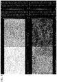
- the additive-containing phase can be observed, for example in the element mapping images ( FIG. 3 ) related to Cu, Ga, and additive element(s) by the electron micro analyzer (EPMA) within the range of 10 mm ⁇ 10 mm, and the grain size (diameter of corresponding circles of the projected area) can be measured accordingly.
- EPMA electron micro analyzer
- Ga in the target is included in the form of an intermetallic compound, for example in the form of Cu-Ga intermetallic compound, in the sputtering target of the present embodiment.
- the elemental substance of Ga exists in the target, the bending strength of the target is reduced to 200 MPa or less. In that case, Ga precipitates as a liquid phase by the processing heat during machining and machining defects are prone to occur. In other words, the cutting-machinability of the sputtering target is improved by avoiding the presence of the elemental substance of Ga in the sputtering target.
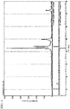
- the presence or absence of the elemental substance of Ga; and the presence or absence of Cu-Ga alloy can be determined by X-ray diffraction (XRD) measurement of the sputtering target, for example ( FIG. 4 ).
- Sodium may be included as NaF compound, Na 2 S compound, or Na 2 Se compound to the sputtering target of the present embodiment.
- the sputtering targets are crashed and subjected to a quantitative analysis of their content amounts using ICP method (Inductively Coupled Plasma Method).
- Li, K, Na, and compounds thereof which are effective for improvement of electrical conversion rate of the solar cell and improvement of cutting-machinability of the target material, can be included in the sputtering target of the present embodiment. It is preferable that the content amounts of Li, K, and Na is in the range of 0.01 to 10 atomic% as the total amount of them. Furthermore, similar effects can be obtained by adding Sb and Bi. The preferable content amount of Sb and Bi is in the range of 0.01 to 10 atomic% as the total amount of them.
- the dissolution casting method and the powder method can be used for producing the sputtering target of the present embodiment.
- the powder method there are the methods in which the raw material powder is sintered after molding if necessary or without molding (hereinafter, referred as "the powder sintering method"); the method in which the raw material powder in a semi-molten state is sprayed on a substrate at high speed and the obtained compact is directly used as a target material; and the method in which the obtained compact is subjected to sintering further to be the target material.
- the sputtering target is produced by the dissolution casting method by performing the processes explained below.
- an ingot with the oxygen content amount of 800 weight ppm or less is produced by melting: at least elementary substances of each of Cu, Ga, and other additive elements; or the alloy containing 2 or more of the above-mentioned elements, at 1050°C or higher.
- the obtained ingot is subjected to a quench casting or a rolling as needed in order to optimize the crystal structure of the obtained ingot.
- the melting point of Cu-Ga-based alloy containing 15 atomic% or more of Ga, and 0.1 atomic% or more of the additive element(s) is(are) 1000°C or less.
- the reason for setting the melting temperature at 1050°C or higher is that if it were lower than 1050°C, the viscosity of the melt including Cu, Ga, and the additive element(s) would be kept at high level, making it difficult for each of the melted elements to be evenly mixed. In other words, miniaturization of the additive-containing phase in the obtained ingot would be difficult. In that case, occurrence of cracking or fracturing during machining of the target material would be increased. Therefore, the melting temperature is set to 1050°C or higher.
- the oxide inclusions would be easily formed by introduction of the additive element(s).
- the presence of the oxide inclusions weakens the bonding between the grains of Cu-Ga alloy. As a result, occurrence of defects on the cut surface is increased during high speed cutting of the target material.
- the dissolution casting method there is no specific limitation for measures to keep the oxygen content amount in the target material to 800 weight ppm or less.
- the dissolution casting method using a vacuum melting furnace; the dissolution casing method in an atmosphere free of oxygen; the dissolution casting method using a carbon crucible or a carbon mold having deoxidizing effect in the air; the dissolution casting method in which the surface of the melt is covered by a deoxidizing material such as carbon particles in the air; the method in which alkaline metal such as lithium metal, sodium metal, or potassium metal is added to the melt for deoxidization; or the like can be used.
- the powder sintering method includes a process of preparing the raw material powder, which includes at least Cu, Ga, and each of the additive elements as an elemental powder; or alloy powder including two or more of Cu, Ga, and each of the additive element(s); and a process of sintering the raw material powder in a vacuum; in an inert atmosphere; or in a reduction atmosphere, by hot pressing (HP) or hot isostatic pressing (HIP).
- a sintering process in which the prepared raw material powder after press-molding is sintered in a vacuum; in an inert atmosphere with an atmospheric pressure of 0.01-10kgf/cm 2 ; or in a reduction atmosphere in a non-pressurized state, can be used. It is preferable that the average grain size of the raw material powder is 1-500 ⁇ m.
- the sintering is performed at HP temperature (the holding temperature in HP) and HIP temperature (the holding temperature in HIP) set in the range of 150-900°C.
- HP temperature the holding temperature in HP
- HIP temperature the holding temperature in HIP
- the reason for setting the temperature range is that if it were lower than 150°C, chipping would be likely to occur during cutting work due to a lowered density of the sintered material; and if it exceeded 900°C, it would cause working defects due to increased average grain size of the Cu-Ga alloy including the additive elements during hot pressing.
- the sintering is performed at the sintering temperature (the holding temperature in sintering) set in the range of 150-950°C.
- the sintering temperature the holding temperature in sintering
- the reason for setting the temperature range is that if it were lower than 150°C, chipping would be likely to occur during cutting work due to a lowered density of the sintered material; and if it exceeded 950°C, it would cause working defects due to increased average grain size of the Cu-Ga alloy including the additive elements.
- Preparation of the raw material powder for performing the above-explained sintering is performed by any one of the processes (a)-(c) described below, for example.
- the raw material powder prepared by any one of the above-described processes (a)-(c) is subjected to HP (hot pressing) or HIP (hot isostatic pressing); or the raw material powder is press-molded. Then, the compact is sintered by sintering or the like. During this sintering process, in order to prevent the Cu-Ga alloy or Cu from being oxidized, it is preferable to perform the sintering in vacuum; in an inert gas atmosphere; or a reduction atmosphere. Pressure in HP and HIP has a substantial impact on density of the sputtering target sintered material. Thus, a preferable pressure for HP is 100-1000kgfcm 2 . A preferable pressure for HIP is 500-1500kgfcm 2 . Pressure may be applied before the beginning of temperature rising during sintering. Alternatively, pressure may be applied after reaching to a given temperature.
- the sputtering target is manufactured by shaping the target material into a predetermined shape by using the cutting method since the Cu-Ga target material including the additive element(s) (or the Cu-Ga target material including the additive element(s) and Na, Li, or K) obtained by the above-described sintering method has an excellent mechanical workability. Then, the sputtering target manufactured as explained above is bonded to a backing place made of Cu or Cu alloy by using In, followed by application to sputtering process.
- the sputtering target In order to prevent the processed sputtering target from being oxidized or taking moisture, it is preferable that the sputtering target to be stored after vacuum packing the whole body of the sputtering target or packing it in a bag with an inert gas replacement.
- Sputtering using this sputtering target of the present embodiment is performed by the direct current (DC) magnetron sputtering method in Ar gas.
- a pulse superposition power supply that applies pulse voltage may be used.
- a DC power supply with no pulse may be used.
- the sputtering target of the present embodiment includes the additive elements and its total amount is 0.1-10 atomic%.
- the sputtering target has a high density ratio, it has high cutting-machinability.
- oxide inclusions of the additive elements are reduced by setting the theoretical density ratio of the sputtering target to 95% or higher and at the same time adjusting the oxygen content to 800 weight ppm or less. Accordingly, the cutting-machinability can be further improved.
- the bending strength of 200 MPa or more can be obtained without occurrence of chipping and fracturing during cutting work.
- Effective implementations in order to obtain the bending strength to 200 MPa or more in the sputtering target are: reduction of casting defects and miniaturization of the metal structure in the production method using the dissolution casting method; and reduction of sintering defects, an appropriate sintering density, and miniaturization of the sintered structure by the sintering condition such as the sintering temperature in the production method using the sintering method.
- the bending strength of 200 MPa or more can be obtained by promoting alloying or even distribution of the additive elements having a low bending strength as an elementary substance in the target, regardless of the dissolution casting method and the sintering method.
- the Cu-Ga film including Na, Li, or K which is effective on improvement of electrical power generation efficiency can be deposited by the sputtering method using the sputtering target including L, K, or Na as: LIF compound; KF compound; NaF compound; Li 2 S compound; K 2 S compound; Na 2 S compound; or a compound of Li 2 Se, K 2 Se, Na 2 Se, Li 2 SeO 3 , K 2 SeO 3 , Na 2 Se 3 , Li 2 Se 4 , K 2 SeO 4 , Na 2 SeO 4 , or the like.
- the contents of fluoride (F) and sulfur (S) in the Cu-Ga film including Li, K, or Na will not be high enough to the extent particularly influencing on the characteristics of the light-absorbing layer of the solar cell.
- Table 1 shows component compositions (at%) of the raw material powders in Reference Examples 1, 2, 6, 8, 10-13, 15-19 and 22-26 and Examples 3-5, 7, 9, 14, 20, 21 and 27-30 of the present invention based on the present embodiments (Ref.Ex. 1, 2, 6, 8, 10-13, 15-19 and 22-26 and Ex.3-5, 7, 9, 14, 20, 21 and 27-30).
- Table 2 shows component compositions (at%) of the raw material powders in Comparative Examples 1-20 (C. Ex. 1-20) for comparison to the Reference Examples and Examples of the present invention.
- Example 5 of the present invention the raw material powder was mixed by dry-ball milling the atomized powder obtained from the Cu-50at%Ga ingot; the same pure Cu powder used in Reference Example 19; and the pure Zn powder having the average grain size of 3 ⁇ m and purity of 99.99% (hereinafter referred as the pure Zn powder).
- the raw material powder was prepared by mixing the Cu-Ga atomized powder with each of powders of the additive element Al, and Bi.
- the average grain size of the used pure Al powder was 125 ⁇ m.
- the average grain size was 308 ⁇ m and purity was 99.9%.
- Example 20 of the present invention the raw material powder was prepared by atomizing Cu, Ga, and Sn; and adding the NAF powder by ball-milling.
- Example 21 of the present invention the raw material powder was prepared by adding the pure Zn powder; and the NaF powder to the Cu-Ga atomized powder, and mixing the obtained material by mixing by dry-ball milling.
- the raw material powder shown in Table 1 was prepared by dry-mixing the Cu-Ga atomized powder; the Al-Sn powder having purity of 99.99% and the average grain size of 234 ⁇ m; and the NAF powder.
- the raw material powder was obtained by mixing the Cu-Ga atomized powder; the Al-Zn powder having purity of 99.99% and the average grain size of 158 ⁇ m; the Sb powder having purity of 99.99% and the average grain size of 260 ⁇ m; and the Na 2 S powder having purity of 99% and the average grain size of 9 ⁇ m (hereinafter referred as the Na 2 S powder).
- the raw material powder was obtained by mixing the Cu-Ga atomized powder; the pure A1 powder; the pure Zn powder; the pure Sn powder having the average grain size of 2 ⁇ m and purity of 99.9% (hereinafter referred as the pure Sn powder); and the Na 2 Se powder having the average grain size of 10 ⁇ m and purity of 98%, by using a rocking mixer.
- Example 29 of the present invention the raw material powder was prepared by adding the pure Zn powder and the KF powder to the Cu-Ga atomized powder and mixing the obtained material by a dry-ball mill.
- Example 30 of the present invention the raw material powder was prepared by adding the pure Zn powder, the pure Mg powder, and the NAF powder to the Cu-Ga atomized powder and mixing the obtained material by a dry-ball mill.
- the raw material powder was prepared by mixing the Cu-Ga atomized powder and the Sn powder evenly by using a V-type mixer.
- the raw material powder was prepared by atomizing each element of Cu, Ga, Al, Zn, Sn and Sb; and mixing the obtained atomized powder and the Na 2 S powder by a ball mill.
- the raw material powder was prepared by mixing the atomized powder from Cu, Ga, Zn, and Bi; and the Na 2 Se powder.
- each of additive elements was inserted into the vacuum melting furnace in order to obtain the compositions shown in Tables 1 and 2. Then, after confirming that it reached to a specified melting temperature and all the metals were melted, it was held for 10 minutes for performing casting. Melting and casting may be performed in a vacuum. Alternatively, they may be performed in an inert gas atmosphere. In the case in the inert gas atmosphere, it is preferable that the pressure of the atmosphere is lower than the atmospheric pressure.
- Example 1 and Examples 27 and 28 of the present invention a water-cooled mold was used for obtaining a small metal cast structure.
- Example 9 of the present invention and Comparative Examples 7-9, 11, 19, and 20 the water-cooled mold was not used, and the materials were left in the vacuum melting furnace after casting in a graphite mold, and natural cooling was performed.
- Example 4 of the present invention and Reference Example 11 the vacuum casting was performed as explained above, the obtained ingot was further subjected to dry-crushing in an inert gas atmosphere to be the material for powder sintering.
- Example 7 of the present invention and Reference Example 13; and Comparative Example 2
- metal molds were filled with the raw material powders. After performing molding at the pressure of 1000kgf/cm 2 , sintering was performed in a pure hydrogen atmosphere with the air pressure of 0.3-1.2.
- the sputtering targets having diameter of 80mm and thickness of 6mm were produced.
- the dimension density of the obtained sputtering target was calculated.
- the results as the calculated theoretical density ratios are shown in Tables 3 and 4.
- the theoretical density ratio was obtained by: melting the metal phase of Cu, Ga, the A1 and other additive element(s), Bi, Sb, Li, or the like in the sputtering target; defining the density of the defect-free ingot obtained by slow cooling as the theoretical density in the specific composition; and obtaining the theoretical density ratio from the ratio of the sputtering target to the above-mentioned theoretical density (target density/theoretical density ⁇ 100%).
- the volume ratio was calculated by using the added amount of the compound phase. Then, the theoretical densities of the metal phase and the Na compound in the sintered material were calculated; and the theoretical density ratio was calculated from the ratio of the dimension density of the target to the sum of them.
- the content amount of each of metal elements in the sputtering target was analyzed using an analytical block collected from the target by ICP method.
- the oxygen content was analyzed using the analytical block by the carbon dioxide absorption method.
- the bending strength of the sputtering target was obtained by measuring the three-point bending strength of the target material based Japanese industrial standard, JIS R1601.
- Observation of the structure of the sputtering target was performed by surface distribution (mapping) measurement of each of elements by EPMA (electron probe micro analyzer, model JXA-8500F, manufactured by JEOL Ltd.) after embedding a piece of the sintered sputtering target in a resin; and wet-polishing to obtain a flat surface.
- the observation was performed in the condition where: the accelerating voltage was 15kV; the irradiation current was 50nA; the scanning type was one-way; the pixels (X, Y) were 240 and 180, respectively; the spot size (X, Y) were 0.1 ⁇ m and 0.1 ⁇ m, respectively; and the measurement time was 10 ms.
- the observation magnification was set to 100-fold, and an area of 10 ⁇ 5mm was subjected to the element distribution (mapping) measurements multiple times separately. Then, the average grain size of the structure with at least the elemental substance of the A1 and other additive element(s) or the intermetallic compound of the A1 and other additive element(s) was confirmed based on the obtained mapping image.
- the results explained above are shown in Tables 5 and 6.
- the target materials of Examples of the present invention and Comparative Examples were subjected to dry-cutting by using the lathe model MS850G manufactured by DMG Mori Seiki Co., Ltd..
- the size was: 80 mm of diameter; and 6 mm of thickness.
- the rate of rotation was 140 rpm.
- the depth of cut was 0.3 mm, and the feeding rate was 0.097mm/rev by the cutting tool.
- the shape model number of the tool bit was STFER1616H16 (manufactured by Mitsubishi Materials Co., Ltd.).
- the shape model number of the insert was TEGX160302L and the kind of the material was HTi10.
- the evaluation of the surface of the sintered material was done after cutting from the surface of each material in the thickness of 1.0 mm.
- the measurement of the surface roughness, and confirmation of the present or absence of fracturing and chipping on the surface due to cutting, were performed in the location 20mm away from the center part of the machined sintered material.
- the surftest model SV-3000 manufactured by Mitutoyo Co., Ltd. was used as a measurement apparatus of the surface roughness.
- the measurement length was 4 mm.
- a photograph of the range of 22cm 2 was taken by a low magnification optical microscope.
- Air-cooling without use water-cooli ng mold in casting 1100 Present 100 Ref.Ex. 17 Air-cooling without use of water-cooli ng mold in casting 1150 Present 100 Ref.Ex. 18 Air-cooling without use water-cooli ng mold in casting 1100 Absent 100 Ref.Ex. 19 HP 300 750 2 98 Ex.20 HIP 1200 750 2 98 Ex.21 HP 200 700 2 96 Ref.Ex. 22 HP 250 360 3 97 Ref.Ex. 23 HIP 1200 550 1 98 Ref.Ex. 24 HIP 1000 500 2 98 Ref.Ex.
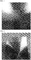
- FIG. 1 a photographic image of the surface of the target in Reference Example 23, which was Cu-30%Ga-3%Zn-3%Na-3%F (atomic %), after cutting work is shown in FIG. 1 .
- a photographic image of the surface of the target in Comparative Example 2 which was Cu-30%Ga-3%Na-3%F (atomic %), after cutting work is shown in FIG. 2 .
- element distribution mapping images by EPMA of the sputtering target of Example 7 of the present invention which was Cu-30%Ga-3%Sn (atomic %), are shown in FIG. 3 .
- the EPMA images were colored images, and they were converted to grey-scaled images. In these converted images, the higher the brightness, the higher the content.
- a sputtering target made of a Cu-Ga alloy can be produced more efficiently.
Priority Applications (1)
| Application Number | Priority Date | Filing Date | Title |
|---|---|---|---|
| EP17196167.5A EP3293284A1 (en) | 2013-02-25 | 2014-02-25 | Sputtering target and method of producing the same |
Applications Claiming Priority (3)
| Application Number | Priority Date | Filing Date | Title |
|---|---|---|---|
| JP2013034389 | 2013-02-25 | ||
| JP2014006532A JP5594618B1 (ja) | 2013-02-25 | 2014-01-17 | スパッタリングターゲット及びその製造方法 |
| PCT/JP2014/054468 WO2014129648A1 (ja) | 2013-02-25 | 2014-02-25 | スパッタリングターゲット及びその製造方法 |
Related Child Applications (2)
| Application Number | Title | Priority Date | Filing Date |
|---|---|---|---|
| EP17196167.5A Division EP3293284A1 (en) | 2013-02-25 | 2014-02-25 | Sputtering target and method of producing the same |
| EP17196167.5A Division-Into EP3293284A1 (en) | 2013-02-25 | 2014-02-25 | Sputtering target and method of producing the same |
Publications (3)
| Publication Number | Publication Date |
|---|---|
| EP2960355A1 EP2960355A1 (en) | 2015-12-30 |
| EP2960355A4 EP2960355A4 (en) | 2017-03-01 |
| EP2960355B1 true EP2960355B1 (en) | 2019-12-04 |
Family
ID=51391424
Family Applications (2)
| Application Number | Title | Priority Date | Filing Date |
|---|---|---|---|
| EP17196167.5A Withdrawn EP3293284A1 (en) | 2013-02-25 | 2014-02-25 | Sputtering target and method of producing the same |
| EP14754195.7A Active EP2960355B1 (en) | 2013-02-25 | 2014-02-25 | Sputtering target and production method therefor |
Family Applications Before (1)
| Application Number | Title | Priority Date | Filing Date |
|---|---|---|---|
| EP17196167.5A Withdrawn EP3293284A1 (en) | 2013-02-25 | 2014-02-25 | Sputtering target and method of producing the same |
Country Status (6)
| Country | Link |
|---|---|
| US (1) | US20160118232A1 (ja) |
| EP (2) | EP3293284A1 (ja) |
| JP (1) | JP5594618B1 (ja) |
| CN (1) | CN105008580B (ja) |
| TW (1) | TWI491749B (ja) |
| WO (1) | WO2014129648A1 (ja) |
Families Citing this family (9)
| Publication number | Priority date | Publication date | Assignee | Title |
|---|---|---|---|---|
| JP6583019B2 (ja) | 2015-03-30 | 2019-10-02 | 三菱マテリアル株式会社 | Cu−Ga合金スパッタリングターゲット、及び、Cu−Ga合金スパッタリングターゲットの製造方法 |
| JP6798852B2 (ja) | 2015-10-26 | 2020-12-09 | 三菱マテリアル株式会社 | スパッタリングターゲット及びスパッタリングターゲットの製造方法 |
| JP6794850B2 (ja) * | 2016-02-08 | 2020-12-02 | 三菱マテリアル株式会社 | スパッタリングターゲット及びスパッタリングターゲットの製造方法 |
| TWI634669B (zh) * | 2016-04-22 | 2018-09-01 | 國立清華大學 | 大面積薄膜太陽能電池的製法 |
| JP2018024933A (ja) * | 2016-07-29 | 2018-02-15 | 三菱マテリアル株式会社 | Cu−Gaスパッタリングターゲット及びCu−Gaスパッタリングターゲットの製造方法 |
| DE102017116972A1 (de) * | 2017-07-27 | 2019-01-31 | Karlsruher Institut für Technologie | Verfahren zur Herstellung einer einphasigen Schicht aus intermetallischen Verbindungen |
| JP6531816B1 (ja) * | 2017-12-22 | 2019-06-19 | 三菱マテリアル株式会社 | Cu−Ga合金スパッタリングターゲット、及び、Cu−Ga合金スパッタリングターゲットの製造方法 |
| JP2019112671A (ja) * | 2017-12-22 | 2019-07-11 | 三菱マテリアル株式会社 | Cu−Ga合金スパッタリングターゲット、及び、Cu−Ga合金スパッタリングターゲットの製造方法 |
| JP2020012190A (ja) * | 2018-07-20 | 2020-01-23 | 株式会社アルバック | 密着膜用ターゲット、配線層、半導体装置、液晶表示装置 |
Family Cites Families (15)
| Publication number | Priority date | Publication date | Assignee | Title |
|---|---|---|---|---|
| JPS60262931A (ja) * | 1984-06-08 | 1985-12-26 | Hitachi Ltd | 分光反射率可変合金 |
| JPS6169934A (ja) * | 1984-09-14 | 1986-04-10 | Hitachi Ltd | 分光反射率可変合金及び記録材料 |
| DD290501A5 (de) * | 1989-12-20 | 1991-05-29 | Zi F. Festkoerperphysik Und Werkstofforschung Der Adw,De | Traegermaterial fuer hochtemperatur-supraleitende schichten |
| JP3249408B2 (ja) | 1996-10-25 | 2002-01-21 | 昭和シェル石油株式会社 | 薄膜太陽電池の薄膜光吸収層の製造方法及び製造装置 |
| JP2000073163A (ja) * | 1998-08-28 | 2000-03-07 | Vacuum Metallurgical Co Ltd | Cu−Ga合金スパッタリングターゲット及びその製造方法 |
| US20040072009A1 (en) * | 1999-12-16 | 2004-04-15 | Segal Vladimir M. | Copper sputtering targets and methods of forming copper sputtering targets |
| WO2007004344A1 (ja) * | 2005-07-04 | 2007-01-11 | Nippon Mining & Metals Co., Ltd. | 光ディスク及びCu合金記録層用スパッタリングターゲット |
| JP5388478B2 (ja) | 2008-05-20 | 2014-01-15 | 株式会社東芝 | 半導体装置 |
| WO2011001974A1 (ja) * | 2009-07-01 | 2011-01-06 | Jx日鉱日石金属株式会社 | Cu-Gaターゲット及びその製造方法 |
| WO2011010529A1 (ja) * | 2009-07-23 | 2011-01-27 | Jx日鉱日石金属株式会社 | Cu-Ga合金焼結体スパッタリングターゲット、同ターゲットの製造方法、Cu-Ga合金焼結体ターゲットから作製された光吸収層及び同光吸収層を用いたCIGS系太陽電池 |
| WO2011013471A1 (ja) * | 2009-07-27 | 2011-02-03 | Jx日鉱日石金属株式会社 | Cu-Ga焼結体スパッタリングターゲット及び同ターゲットの製造方法 |
| JP5501774B2 (ja) * | 2010-01-20 | 2014-05-28 | 山陽特殊製鋼株式会社 | 高強度を有するCu−Ga系スパッタリングターゲット材 |
| JP4831258B2 (ja) * | 2010-03-18 | 2011-12-07 | 三菱マテリアル株式会社 | スパッタリングターゲット及びその製造方法 |
| JP2012017481A (ja) * | 2010-07-06 | 2012-01-26 | Mitsui Mining & Smelting Co Ltd | Cu−Ga合金およびCu−Ga合金スパッタリングターゲット |
| JP5153911B2 (ja) * | 2011-04-22 | 2013-02-27 | 三菱マテリアル株式会社 | スパッタリングターゲット及びその製造方法 |
-
2014
- 2014-01-17 JP JP2014006532A patent/JP5594618B1/ja active Active
- 2014-02-25 TW TW103106263A patent/TWI491749B/zh not_active IP Right Cessation
- 2014-02-25 US US14/769,898 patent/US20160118232A1/en not_active Abandoned
- 2014-02-25 EP EP17196167.5A patent/EP3293284A1/en not_active Withdrawn
- 2014-02-25 CN CN201480010218.3A patent/CN105008580B/zh not_active Expired - Fee Related
- 2014-02-25 WO PCT/JP2014/054468 patent/WO2014129648A1/ja active Application Filing
- 2014-02-25 EP EP14754195.7A patent/EP2960355B1/en active Active
Non-Patent Citations (1)
| Title |
|---|
| None * |
Also Published As
| Publication number | Publication date |
|---|---|
| TW201446989A (zh) | 2014-12-16 |
| JP5594618B1 (ja) | 2014-09-24 |
| CN105008580B (zh) | 2018-12-04 |
| US20160118232A1 (en) | 2016-04-28 |
| EP2960355A4 (en) | 2017-03-01 |
| EP3293284A1 (en) | 2018-03-14 |
| CN105008580A (zh) | 2015-10-28 |
| WO2014129648A1 (ja) | 2014-08-28 |
| EP2960355A1 (en) | 2015-12-30 |
| TWI491749B (zh) | 2015-07-11 |
| JP2014185392A (ja) | 2014-10-02 |
Similar Documents
| Publication | Publication Date | Title |
|---|---|---|
| EP2960355B1 (en) | Sputtering target and production method therefor | |
| EP2784173B1 (en) | Sputtering target and method for producing same | |
| EP3369842B1 (en) | Sputtering target and method for producing sputtering target | |
| KR101358345B1 (ko) | 스퍼터링 타겟 및 그 제조방법 | |
| JP6176535B2 (ja) | スパッタリングターゲット及びその製造方法 | |
| EP2666884A1 (en) | Cu-ga target and method for manufacturing same, as well as light-absorbing layer formed from cu-ga alloy film, and cigs solar cell using light-absorbing layer | |
| JP6634750B2 (ja) | スパッタリングターゲット及びその製造方法 | |
| JP6311912B2 (ja) | Cu−Ga二元系スパッタリングターゲット及びその製造方法 | |
| WO2016047556A1 (ja) | スパッタリングターゲット及びその製造方法 |
Legal Events
| Date | Code | Title | Description |
|---|---|---|---|
| PUAI | Public reference made under article 153(3) epc to a published international application that has entered the european phase |
Free format text: ORIGINAL CODE: 0009012 |
|
| 17P | Request for examination filed |
Effective date: 20150923 |
|
| AK | Designated contracting states |
Kind code of ref document: A1 Designated state(s): AL AT BE BG CH CY CZ DE DK EE ES FI FR GB GR HR HU IE IS IT LI LT LU LV MC MK MT NL NO PL PT RO RS SE SI SK SM TR |
|
| AX | Request for extension of the european patent |
Extension state: BA ME |
|
| DAX | Request for extension of the european patent (deleted) | ||
| RIC1 | Information provided on ipc code assigned before grant |
Ipc: C22C 28/00 20060101ALI20160909BHEP Ipc: C22F 1/16 20060101ALI20160909BHEP Ipc: C22F 1/00 20060101ALI20160909BHEP Ipc: B22F 3/15 20060101ALI20160909BHEP Ipc: C22F 1/08 20060101ALI20160909BHEP Ipc: C23C 14/34 20060101AFI20160909BHEP Ipc: B22F 3/14 20060101ALI20160909BHEP Ipc: C22C 1/04 20060101ALI20160909BHEP Ipc: C22C 9/00 20060101ALI20160909BHEP |
|
| A4 | Supplementary search report drawn up and despatched |
Effective date: 20170130 |
|
| RIC1 | Information provided on ipc code assigned before grant |
Ipc: C22C 28/00 20060101ALI20170124BHEP Ipc: C23C 14/34 20060101AFI20170124BHEP Ipc: C22C 9/00 20060101ALI20170124BHEP Ipc: B22F 3/14 20060101ALI20170124BHEP Ipc: C22F 1/08 20060101ALI20170124BHEP Ipc: B22F 3/15 20060101ALI20170124BHEP Ipc: C22C 1/04 20060101ALI20170124BHEP Ipc: C22F 1/00 20060101ALI20170124BHEP Ipc: C22F 1/16 20060101ALI20170124BHEP |
|
| STAA | Information on the status of an ep patent application or granted ep patent |
Free format text: STATUS: EXAMINATION IS IN PROGRESS |
|
| 17Q | First examination report despatched |
Effective date: 20180205 |
|
| RAP1 | Party data changed (applicant data changed or rights of an application transferred) |
Owner name: MITSUBISHI MATERIALS CORPORATION |
|
| GRAP | Despatch of communication of intention to grant a patent |
Free format text: ORIGINAL CODE: EPIDOSNIGR1 |
|
| STAA | Information on the status of an ep patent application or granted ep patent |
Free format text: STATUS: GRANT OF PATENT IS INTENDED |
|
| INTG | Intention to grant announced |
Effective date: 20190819 |
|
| GRAS | Grant fee paid |
Free format text: ORIGINAL CODE: EPIDOSNIGR3 |
|
| GRAA | (expected) grant |
Free format text: ORIGINAL CODE: 0009210 |
|
| STAA | Information on the status of an ep patent application or granted ep patent |
Free format text: STATUS: THE PATENT HAS BEEN GRANTED |
|
| AK | Designated contracting states |
Kind code of ref document: B1 Designated state(s): AL AT BE BG CH CY CZ DE DK EE ES FI FR GB GR HR HU IE IS IT LI LT LU LV MC MK MT NL NO PL PT RO RS SE SI SK SM TR |
|
| REG | Reference to a national code |
Ref country code: GB Ref legal event code: FG4D |
|
| REG | Reference to a national code |
Ref country code: CH Ref legal event code: EP |
|
| REG | Reference to a national code |
Ref country code: AT Ref legal event code: REF Ref document number: 1209501 Country of ref document: AT Kind code of ref document: T Effective date: 20191215 |
|
| REG | Reference to a national code |
Ref country code: DE Ref legal event code: R096 Ref document number: 602014057821 Country of ref document: DE |
|
| REG | Reference to a national code |
Ref country code: IE Ref legal event code: FG4D |
|
| REG | Reference to a national code |
Ref country code: NL Ref legal event code: MP Effective date: 20191204 |
|
| REG | Reference to a national code |
Ref country code: LT Ref legal event code: MG4D |
|
| PG25 | Lapsed in a contracting state [announced via postgrant information from national office to epo] |
Ref country code: LV Free format text: LAPSE BECAUSE OF FAILURE TO SUBMIT A TRANSLATION OF THE DESCRIPTION OR TO PAY THE FEE WITHIN THE PRESCRIBED TIME-LIMIT Effective date: 20191204 Ref country code: SE Free format text: LAPSE BECAUSE OF FAILURE TO SUBMIT A TRANSLATION OF THE DESCRIPTION OR TO PAY THE FEE WITHIN THE PRESCRIBED TIME-LIMIT Effective date: 20191204 Ref country code: BG Free format text: LAPSE BECAUSE OF FAILURE TO SUBMIT A TRANSLATION OF THE DESCRIPTION OR TO PAY THE FEE WITHIN THE PRESCRIBED TIME-LIMIT Effective date: 20200304 Ref country code: FI Free format text: LAPSE BECAUSE OF FAILURE TO SUBMIT A TRANSLATION OF THE DESCRIPTION OR TO PAY THE FEE WITHIN THE PRESCRIBED TIME-LIMIT Effective date: 20191204 Ref country code: NO Free format text: LAPSE BECAUSE OF FAILURE TO SUBMIT A TRANSLATION OF THE DESCRIPTION OR TO PAY THE FEE WITHIN THE PRESCRIBED TIME-LIMIT Effective date: 20200304 Ref country code: GR Free format text: LAPSE BECAUSE OF FAILURE TO SUBMIT A TRANSLATION OF THE DESCRIPTION OR TO PAY THE FEE WITHIN THE PRESCRIBED TIME-LIMIT Effective date: 20200305 Ref country code: LT Free format text: LAPSE BECAUSE OF FAILURE TO SUBMIT A TRANSLATION OF THE DESCRIPTION OR TO PAY THE FEE WITHIN THE PRESCRIBED TIME-LIMIT Effective date: 20191204 |
|
| PG25 | Lapsed in a contracting state [announced via postgrant information from national office to epo] |
Ref country code: RS Free format text: LAPSE BECAUSE OF FAILURE TO SUBMIT A TRANSLATION OF THE DESCRIPTION OR TO PAY THE FEE WITHIN THE PRESCRIBED TIME-LIMIT Effective date: 20191204 Ref country code: HR Free format text: LAPSE BECAUSE OF FAILURE TO SUBMIT A TRANSLATION OF THE DESCRIPTION OR TO PAY THE FEE WITHIN THE PRESCRIBED TIME-LIMIT Effective date: 20191204 |
|
| PG25 | Lapsed in a contracting state [announced via postgrant information from national office to epo] |
Ref country code: AL Free format text: LAPSE BECAUSE OF FAILURE TO SUBMIT A TRANSLATION OF THE DESCRIPTION OR TO PAY THE FEE WITHIN THE PRESCRIBED TIME-LIMIT Effective date: 20191204 |
|
| PG25 | Lapsed in a contracting state [announced via postgrant information from national office to epo] |
Ref country code: EE Free format text: LAPSE BECAUSE OF FAILURE TO SUBMIT A TRANSLATION OF THE DESCRIPTION OR TO PAY THE FEE WITHIN THE PRESCRIBED TIME-LIMIT Effective date: 20191204 Ref country code: CZ Free format text: LAPSE BECAUSE OF FAILURE TO SUBMIT A TRANSLATION OF THE DESCRIPTION OR TO PAY THE FEE WITHIN THE PRESCRIBED TIME-LIMIT Effective date: 20191204 Ref country code: RO Free format text: LAPSE BECAUSE OF FAILURE TO SUBMIT A TRANSLATION OF THE DESCRIPTION OR TO PAY THE FEE WITHIN THE PRESCRIBED TIME-LIMIT Effective date: 20191204 Ref country code: NL Free format text: LAPSE BECAUSE OF FAILURE TO SUBMIT A TRANSLATION OF THE DESCRIPTION OR TO PAY THE FEE WITHIN THE PRESCRIBED TIME-LIMIT Effective date: 20191204 Ref country code: ES Free format text: LAPSE BECAUSE OF FAILURE TO SUBMIT A TRANSLATION OF THE DESCRIPTION OR TO PAY THE FEE WITHIN THE PRESCRIBED TIME-LIMIT Effective date: 20191204 Ref country code: PT Free format text: LAPSE BECAUSE OF FAILURE TO SUBMIT A TRANSLATION OF THE DESCRIPTION OR TO PAY THE FEE WITHIN THE PRESCRIBED TIME-LIMIT Effective date: 20200429 |
|
| PG25 | Lapsed in a contracting state [announced via postgrant information from national office to epo] |
Ref country code: SK Free format text: LAPSE BECAUSE OF FAILURE TO SUBMIT A TRANSLATION OF THE DESCRIPTION OR TO PAY THE FEE WITHIN THE PRESCRIBED TIME-LIMIT Effective date: 20191204 Ref country code: SM Free format text: LAPSE BECAUSE OF FAILURE TO SUBMIT A TRANSLATION OF THE DESCRIPTION OR TO PAY THE FEE WITHIN THE PRESCRIBED TIME-LIMIT Effective date: 20191204 Ref country code: IS Free format text: LAPSE BECAUSE OF FAILURE TO SUBMIT A TRANSLATION OF THE DESCRIPTION OR TO PAY THE FEE WITHIN THE PRESCRIBED TIME-LIMIT Effective date: 20200404 |
|
| REG | Reference to a national code |
Ref country code: DE Ref legal event code: R097 Ref document number: 602014057821 Country of ref document: DE |
|
| REG | Reference to a national code |
Ref country code: AT Ref legal event code: MK05 Ref document number: 1209501 Country of ref document: AT Kind code of ref document: T Effective date: 20191204 |
|
| REG | Reference to a national code |
Ref country code: CH Ref legal event code: PL |
|
| PLBE | No opposition filed within time limit |
Free format text: ORIGINAL CODE: 0009261 |
|
| STAA | Information on the status of an ep patent application or granted ep patent |
Free format text: STATUS: NO OPPOSITION FILED WITHIN TIME LIMIT |
|
| REG | Reference to a national code |
Ref country code: BE Ref legal event code: MM Effective date: 20200229 |
|
| PG25 | Lapsed in a contracting state [announced via postgrant information from national office to epo] |
Ref country code: MC Free format text: LAPSE BECAUSE OF FAILURE TO SUBMIT A TRANSLATION OF THE DESCRIPTION OR TO PAY THE FEE WITHIN THE PRESCRIBED TIME-LIMIT Effective date: 20191204 Ref country code: DK Free format text: LAPSE BECAUSE OF FAILURE TO SUBMIT A TRANSLATION OF THE DESCRIPTION OR TO PAY THE FEE WITHIN THE PRESCRIBED TIME-LIMIT Effective date: 20191204 Ref country code: LU Free format text: LAPSE BECAUSE OF NON-PAYMENT OF DUE FEES Effective date: 20200225 |
|
| 26N | No opposition filed |
Effective date: 20200907 |
|
| PG25 | Lapsed in a contracting state [announced via postgrant information from national office to epo] |
Ref country code: LI Free format text: LAPSE BECAUSE OF NON-PAYMENT OF DUE FEES Effective date: 20200229 Ref country code: SI Free format text: LAPSE BECAUSE OF FAILURE TO SUBMIT A TRANSLATION OF THE DESCRIPTION OR TO PAY THE FEE WITHIN THE PRESCRIBED TIME-LIMIT Effective date: 20191204 Ref country code: AT Free format text: LAPSE BECAUSE OF FAILURE TO SUBMIT A TRANSLATION OF THE DESCRIPTION OR TO PAY THE FEE WITHIN THE PRESCRIBED TIME-LIMIT Effective date: 20191204 Ref country code: PL Free format text: LAPSE BECAUSE OF FAILURE TO SUBMIT A TRANSLATION OF THE DESCRIPTION OR TO PAY THE FEE WITHIN THE PRESCRIBED TIME-LIMIT Effective date: 20191204 Ref country code: CH Free format text: LAPSE BECAUSE OF NON-PAYMENT OF DUE FEES Effective date: 20200229 |
|
| PG25 | Lapsed in a contracting state [announced via postgrant information from national office to epo] |
Ref country code: FR Free format text: LAPSE BECAUSE OF NON-PAYMENT OF DUE FEES Effective date: 20200229 Ref country code: IT Free format text: LAPSE BECAUSE OF FAILURE TO SUBMIT A TRANSLATION OF THE DESCRIPTION OR TO PAY THE FEE WITHIN THE PRESCRIBED TIME-LIMIT Effective date: 20191204 Ref country code: IE Free format text: LAPSE BECAUSE OF NON-PAYMENT OF DUE FEES Effective date: 20200225 |
|
| PG25 | Lapsed in a contracting state [announced via postgrant information from national office to epo] |
Ref country code: BE Free format text: LAPSE BECAUSE OF NON-PAYMENT OF DUE FEES Effective date: 20200229 |
|
| GBPC | Gb: european patent ceased through non-payment of renewal fee |
Effective date: 20200304 |
|
| PG25 | Lapsed in a contracting state [announced via postgrant information from national office to epo] |
Ref country code: GB Free format text: LAPSE BECAUSE OF NON-PAYMENT OF DUE FEES Effective date: 20200304 |
|
| PGFP | Annual fee paid to national office [announced via postgrant information from national office to epo] |
Ref country code: DE Payment date: 20220217 Year of fee payment: 9 |
|
| PG25 | Lapsed in a contracting state [announced via postgrant information from national office to epo] |
Ref country code: TR Free format text: LAPSE BECAUSE OF FAILURE TO SUBMIT A TRANSLATION OF THE DESCRIPTION OR TO PAY THE FEE WITHIN THE PRESCRIBED TIME-LIMIT Effective date: 20191204 Ref country code: MT Free format text: LAPSE BECAUSE OF FAILURE TO SUBMIT A TRANSLATION OF THE DESCRIPTION OR TO PAY THE FEE WITHIN THE PRESCRIBED TIME-LIMIT Effective date: 20191204 Ref country code: CY Free format text: LAPSE BECAUSE OF FAILURE TO SUBMIT A TRANSLATION OF THE DESCRIPTION OR TO PAY THE FEE WITHIN THE PRESCRIBED TIME-LIMIT Effective date: 20191204 |
|
| PG25 | Lapsed in a contracting state [announced via postgrant information from national office to epo] |
Ref country code: MK Free format text: LAPSE BECAUSE OF FAILURE TO SUBMIT A TRANSLATION OF THE DESCRIPTION OR TO PAY THE FEE WITHIN THE PRESCRIBED TIME-LIMIT Effective date: 20191204 |
|
| REG | Reference to a national code |
Ref country code: DE Ref legal event code: R119 Ref document number: 602014057821 Country of ref document: DE |
|
| PG25 | Lapsed in a contracting state [announced via postgrant information from national office to epo] |
Ref country code: DE Free format text: LAPSE BECAUSE OF NON-PAYMENT OF DUE FEES Effective date: 20230901 |