EP2808902A1 - Dispositif de conversion photoélectrique - Google Patents
Dispositif de conversion photoélectrique Download PDFInfo
- Publication number
- EP2808902A1 EP2808902A1 EP12866499.2A EP12866499A EP2808902A1 EP 2808902 A1 EP2808902 A1 EP 2808902A1 EP 12866499 A EP12866499 A EP 12866499A EP 2808902 A1 EP2808902 A1 EP 2808902A1
- Authority
- EP
- European Patent Office
- Prior art keywords
- semiconductor layer
- photoelectric conversion
- layer
- conversion device
- crystal grains
- Prior art date
- Legal status (The legal status is an assumption and is not a legal conclusion. Google has not performed a legal analysis and makes no representation as to the accuracy of the status listed.)
- Withdrawn
Links
- 238000006243 chemical reaction Methods 0.000 title claims abstract description 61
- 239000004065 semiconductor Substances 0.000 claims abstract description 124
- 239000013078 crystal Substances 0.000 claims abstract description 32
- 150000001875 compounds Chemical class 0.000 claims description 19
- 239000010410 layer Substances 0.000 description 157
- 239000004020 conductor Substances 0.000 description 16
- 239000000758 substrate Substances 0.000 description 13
- 229910052751 metal Inorganic materials 0.000 description 9
- 239000002184 metal Substances 0.000 description 9
- 238000000034 method Methods 0.000 description 8
- 239000002243 precursor Substances 0.000 description 6
- 238000009826 distribution Methods 0.000 description 5
- 238000004544 sputter deposition Methods 0.000 description 5
- 229910052725 zinc Inorganic materials 0.000 description 5
- HVMJUDPAXRRVQO-UHFFFAOYSA-N copper indium Chemical compound [Cu].[In] HVMJUDPAXRRVQO-UHFFFAOYSA-N 0.000 description 4
- ZZEMEJKDTZOXOI-UHFFFAOYSA-N digallium;selenium(2-) Chemical compound [Ga+3].[Ga+3].[Se-2].[Se-2].[Se-2] ZZEMEJKDTZOXOI-UHFFFAOYSA-N 0.000 description 4
- 239000010408 film Substances 0.000 description 4
- 238000010438 heat treatment Methods 0.000 description 4
- 239000000843 powder Substances 0.000 description 4
- 238000000224 chemical solution deposition Methods 0.000 description 3
- 239000011521 glass Substances 0.000 description 3
- 229910052738 indium Inorganic materials 0.000 description 3
- 239000011347 resin Substances 0.000 description 3
- 229920005989 resin Polymers 0.000 description 3
- BWGNESOTFCXPMA-UHFFFAOYSA-N Dihydrogen disulfide Chemical compound SS BWGNESOTFCXPMA-UHFFFAOYSA-N 0.000 description 2
- 239000011230 binding agent Substances 0.000 description 2
- 238000005229 chemical vapour deposition Methods 0.000 description 2
- 239000010949 copper Substances 0.000 description 2
- XLYOFNOQVPJJNP-UHFFFAOYSA-M hydroxide Chemical compound [OH-] XLYOFNOQVPJJNP-UHFFFAOYSA-M 0.000 description 2
- 238000004519 manufacturing process Methods 0.000 description 2
- 230000004048 modification Effects 0.000 description 2
- 238000012986 modification Methods 0.000 description 2
- 230000000149 penetrating effect Effects 0.000 description 2
- 238000005215 recombination Methods 0.000 description 2
- 230000006798 recombination Effects 0.000 description 2
- 239000010409 thin film Substances 0.000 description 2
- 229910004613 CdTe Inorganic materials 0.000 description 1
- 229910017612 Cu(In,Ga)Se2 Inorganic materials 0.000 description 1
- 229910002475 Cu2ZnSnS4 Inorganic materials 0.000 description 1
- 229910018038 Cu2ZnSnSe4 Inorganic materials 0.000 description 1
- UCKMPCXJQFINFW-UHFFFAOYSA-N Sulphide Chemical compound [S-2] UCKMPCXJQFINFW-UHFFFAOYSA-N 0.000 description 1
- KTSFMFGEAAANTF-UHFFFAOYSA-N [Cu].[Se].[Se].[In] Chemical compound [Cu].[Se].[Se].[In] KTSFMFGEAAANTF-UHFFFAOYSA-N 0.000 description 1
- 229910052782 aluminium Inorganic materials 0.000 description 1
- 229910052795 boron group element Inorganic materials 0.000 description 1
- 229910052800 carbon group element Inorganic materials 0.000 description 1
- 239000000919 ceramic Substances 0.000 description 1
- 229910052798 chalcogen Inorganic materials 0.000 description 1
- 150000004770 chalcogenides Chemical class 0.000 description 1
- 238000000576 coating method Methods 0.000 description 1
- 230000003247 decreasing effect Effects 0.000 description 1
- 238000000151 deposition Methods 0.000 description 1
- 238000001704 evaporation Methods 0.000 description 1
- 229910052733 gallium Inorganic materials 0.000 description 1
- 229910001849 group 12 element Inorganic materials 0.000 description 1
- 239000000463 material Substances 0.000 description 1
- 150000002739 metals Chemical class 0.000 description 1
- 229910052750 molybdenum Inorganic materials 0.000 description 1
- 238000010248 power generation Methods 0.000 description 1
- 239000002994 raw material Substances 0.000 description 1
- 150000004771 selenides Chemical class 0.000 description 1
- 229910052711 selenium Inorganic materials 0.000 description 1
- 238000000926 separation method Methods 0.000 description 1
- 239000005361 soda-lime glass Substances 0.000 description 1
- 230000035882 stress Effects 0.000 description 1
- 229910052717 sulfur Inorganic materials 0.000 description 1
- 239000002344 surface layer Substances 0.000 description 1
- 230000008646 thermal stress Effects 0.000 description 1
- 229910052719 titanium Inorganic materials 0.000 description 1
- 238000002834 transmittance Methods 0.000 description 1
Images

Classifications
-
- H—ELECTRICITY
- H10—SEMICONDUCTOR DEVICES; ELECTRIC SOLID-STATE DEVICES NOT OTHERWISE PROVIDED FOR
- H10F—INORGANIC SEMICONDUCTOR DEVICES SENSITIVE TO INFRARED RADIATION, LIGHT, ELECTROMAGNETIC RADIATION OF SHORTER WAVELENGTH OR CORPUSCULAR RADIATION
- H10F77/00—Constructional details of devices covered by this subclass
- H10F77/10—Semiconductor bodies
- H10F77/16—Material structures, e.g. crystalline structures, film structures or crystal plane orientations
- H10F77/162—Non-monocrystalline materials, e.g. semiconductor particles embedded in insulating materials
- H10F77/164—Polycrystalline semiconductors
-
- H—ELECTRICITY
- H10—SEMICONDUCTOR DEVICES; ELECTRIC SOLID-STATE DEVICES NOT OTHERWISE PROVIDED FOR
- H10F—INORGANIC SEMICONDUCTOR DEVICES SENSITIVE TO INFRARED RADIATION, LIGHT, ELECTROMAGNETIC RADIATION OF SHORTER WAVELENGTH OR CORPUSCULAR RADIATION
- H10F19/00—Integrated devices, or assemblies of multiple devices, comprising at least one photovoltaic cell covered by group H10F10/00, e.g. photovoltaic modules
- H10F19/30—Integrated devices, or assemblies of multiple devices, comprising at least one photovoltaic cell covered by group H10F10/00, e.g. photovoltaic modules comprising thin-film photovoltaic cells
- H10F19/31—Integrated devices, or assemblies of multiple devices, comprising at least one photovoltaic cell covered by group H10F10/00, e.g. photovoltaic modules comprising thin-film photovoltaic cells having multiple laterally adjacent thin-film photovoltaic cells deposited on the same substrate
- H10F19/35—Structures for the connecting of adjacent photovoltaic cells, e.g. interconnections or insulating spacers
-
- H—ELECTRICITY
- H10—SEMICONDUCTOR DEVICES; ELECTRIC SOLID-STATE DEVICES NOT OTHERWISE PROVIDED FOR
- H10F—INORGANIC SEMICONDUCTOR DEVICES SENSITIVE TO INFRARED RADIATION, LIGHT, ELECTROMAGNETIC RADIATION OF SHORTER WAVELENGTH OR CORPUSCULAR RADIATION
- H10F77/00—Constructional details of devices covered by this subclass
- H10F77/10—Semiconductor bodies
- H10F77/12—Active materials
- H10F77/126—Active materials comprising only Group I-III-VI chalcopyrite materials, e.g. CuInSe2, CuGaSe2 or CuInGaSe2 [CIGS]
-
- H—ELECTRICITY
- H10—SEMICONDUCTOR DEVICES; ELECTRIC SOLID-STATE DEVICES NOT OTHERWISE PROVIDED FOR
- H10F—INORGANIC SEMICONDUCTOR DEVICES SENSITIVE TO INFRARED RADIATION, LIGHT, ELECTROMAGNETIC RADIATION OF SHORTER WAVELENGTH OR CORPUSCULAR RADIATION
- H10F77/00—Constructional details of devices covered by this subclass
- H10F77/10—Semiconductor bodies
- H10F77/16—Material structures, e.g. crystalline structures, film structures or crystal plane orientations
- H10F77/169—Thin semiconductor films on metallic or insulating substrates
- H10F77/1694—Thin semiconductor films on metallic or insulating substrates the films including Group I-III-VI materials, e.g. CIS or CIGS
-
- H—ELECTRICITY
- H10—SEMICONDUCTOR DEVICES; ELECTRIC SOLID-STATE DEVICES NOT OTHERWISE PROVIDED FOR
- H10F—INORGANIC SEMICONDUCTOR DEVICES SENSITIVE TO INFRARED RADIATION, LIGHT, ELECTROMAGNETIC RADIATION OF SHORTER WAVELENGTH OR CORPUSCULAR RADIATION
- H10F77/00—Constructional details of devices covered by this subclass
- H10F77/10—Semiconductor bodies
- H10F77/16—Material structures, e.g. crystalline structures, film structures or crystal plane orientations
- H10F77/169—Thin semiconductor films on metallic or insulating substrates
- H10F77/1696—Thin semiconductor films on metallic or insulating substrates the films including Group II-VI materials, e.g. CdTe or CdS
-
- Y—GENERAL TAGGING OF NEW TECHNOLOGICAL DEVELOPMENTS; GENERAL TAGGING OF CROSS-SECTIONAL TECHNOLOGIES SPANNING OVER SEVERAL SECTIONS OF THE IPC; TECHNICAL SUBJECTS COVERED BY FORMER USPC CROSS-REFERENCE ART COLLECTIONS [XRACs] AND DIGESTS
- Y02—TECHNOLOGIES OR APPLICATIONS FOR MITIGATION OR ADAPTATION AGAINST CLIMATE CHANGE
- Y02E—REDUCTION OF GREENHOUSE GAS [GHG] EMISSIONS, RELATED TO ENERGY GENERATION, TRANSMISSION OR DISTRIBUTION
- Y02E10/00—Energy generation through renewable energy sources
- Y02E10/50—Photovoltaic [PV] energy
- Y02E10/541—CuInSe2 material PV cells
Definitions
- the present invention relates to a photoelectric conversion device including a polycrystalline semiconductor.
- a photoelectric conversion device to be used for solar photovoltaic power generation a device provided with a plurality of photoelectric conversion cells on a substrate is exemplified as disclosed in Japanese Unexamined Patent Application Publication No. 2000-299486 .
- Such a photoelectric conversion device is formed by two-dimensionally arranging a plurality of photoelectric conversion cells in which a lower electrode layer such as a metal electrode, a light-absorbing layer, a buffer layer, and a transparent conductive film are stacked in this order on a substrate such as glass.
- the plurality of photoelectric conversion cells are electrically connected in series by connecting the transparent conductive film of one of the adjacent photoelectric conversion cells and the lower electrode layer of the other of the adjacent photoelectric conversion cells through a connection conductor.
- a method of increasing the size of crystal grains of a semiconductor layer serving as a light-absorbing layer may be considered as a method for improving the photoelectric conversion efficiency.
- the size of the crystal grains of the semiconductor layer is increased, cracks easily appear on the semiconductor layer due to thermal stress or the like and it is difficult to sufficiently improve the photoelectric conversion efficiency.
- An object of the present invention is to improve photoelectric conversion efficiency of a photoelectric conversion device.
- a photoelectric conversion device comprises an electrode layer; a first semiconductor layer disposed on the electrode layer and including a polycrystalline semiconductor; and a second semiconductor layer disposed on the first semiconductor layer and forming a pn junction with the first semiconductor layer.
- An average grain diameter of crystal grains in the first semiconductor layer is larger in a surface portion on the electrode layer side than in a central portion of the first semiconductor layer in a stacking direction.
- the photoelectric conversion efficiency in the photoelectric conversion device is improved.
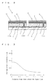
- Fig. 1 is a perspective view illustrating an example of a photoelectric conversion device according to an embodiment of the present invention and Fig. 2 is a cross-sectional view thereof.
- a photoelectric conversion device 11 a plurality of photoelectric conversion cells 10 are arranged on a substrate 1 and are electrically connected to one another. Although only two photoelectric conversion cells 10 are illustrated in Fig. 1 for convenience of illustration, multiple photoelectric conversion cells 10 may be two-dimensionally arranged in the right-left direction in Fig. 1 or further in a direction perpendicular to the right-left direction in the actual photoelectric conversion device 11.
- a plurality of lower electrode layers 2 are two-dimensionally arranged on the substrate 1.
- the plurality of lower electrode layers 2 include lower electrode layers 2a to 2c arranged in one direction with a gap between them.
- a first semiconductor layer 3 is disposed over the lower electrode layer 2a and the lower electrode layer 2b through a portion on the substrate 1.
- a second semiconductor layer 4 whose conductivity type is different from that of the first semiconductor layer 3 is disposed on the first semiconductor layer 3.
- a connection conductor 7 is disposed on the lower electrode layer 2b along the surface (side surface) of the first semiconductor layer 3 or by penetrating the first semiconductor layer 3.
- connection conductor 7 electrically connects the second semiconductor layer 4 and the lower electrode layer 2b.
- One photoelectric conversion cell 10 is formed of the lower electrode layer 2, the first semiconductor layer 3, the second semiconductor layer 4, and an upper electrode layer 5, and a high-output photoelectric conversion device 11 is configured by connecting adjacent photoelectric conversion cells 10 in series through the connection conductor 7.
- a high-output photoelectric conversion device 11 is configured by connecting adjacent photoelectric conversion cells 10 in series through the connection conductor 7.
- the substrate 1 supports the photoelectric conversion cells 10.
- Examples of a material to be used for the substrate 1 include glass, ceramics, resins, metals, and the like.
- soda lime glass having a thickness of approximately 1 mm to 3 mm can be used.
- the lower electrode layers 2 are conductors such as Mo, Al, Ti, or Au disposed on the substrate 1.
- the lower electrode layers 2 are formed to have a thickness of approximately 0.2 ⁇ m to 1 ⁇ m using a known thin film forming method such as a sputtering method or a deposition method.
- the first semiconductor layer 3 includes a semiconductor having a polycrystalline structure.
- the first semiconductor layer 3 has a thickness of, for example, approximately 1 ⁇ m to 3 ⁇ m.
- Examples of the first semiconductor layer 3 include metal chalcogenide such as a group II-VI compound, a group I-III-VI compound, and a group I-II-IV-VI compound.
- the group II-VI compound is a compound semiconductor of group II-B elements (also referred to as group 12 elements) and group VI-B elements (also referred to as group 16 elements).
- group II-VI compound CdTe and the like are exemplified.
- the group I-III-VI compound is a compound of group I-B elements (also referred to as group 11 elements), group III-B elements (also referred to as group 13 elements), and group VI-B elements.
- Examples of the group I-III-VI compound include CuInSe 2 (copper indium diselenide, also referred to as CIS), Cu(In,Ga)Se 2 (copper indium gallium diselenide, also referred to as CIGS), and Cu(In,Ga)(Se,S) 2 (copper indium gallium diselenide disulfide, also referred to as CIGSS).
- the first semiconductor layer 3 may be formed of a multiple compound semiconductor thin film such as copper indium gallium diselenide provided with a thin copper indium gallium diselenide disulfide layer as a surface layer.
- the group I-II-IV-VI compound is a compound of group I-B elements, group II-B elements, group IV-B elements (also referred to as group 14 elements), and group VI-B elements.
- Examples of the group I-II-IV-VI compound include Cu 2 ZnSnS 4 (also referred to as CZTS), Cu 2 ZnSn(S,Se) 4 (also referred to as CZTSSe), and Cu 2 ZnSnSe 4 (also referred to as CZTSe).
- the average grain diameter of crystal grains of the first semiconductor layer 3 is larger in the surface portion on the lower electrode layer 2 side than in the central portion of the first semiconductor layer 3 in the thickness direction (stacking direction).
- the average grain diameter of crystal grains of the surface portion on the lower electrode layer 2 side is larger than that of the crystal grains of the central portion, in a case where the first semiconductor layer 3 is assumed to be divided into the surface portion on the lower electrode layer 2 side, the central portion, and the surface portion on the second semiconductor layer 4 side by being trisected in the thickness direction.
- the average grain diameter of crystal grains is acquired as follows. First, in regard to the cross sections of respective layers trisected as described above, images (also referred to as cross-sectional images) are obtained by photographing 10 arbitrary sites without concentrating at particular regions with a scanning electron microscope (SEM). Next, grain diameters of a plurality of grains are determined using image processing software or the like, from electronic data of the images or data in which the photographed images are captured by a scanner, and the average grain diameters of the crystal grains are calculated by acquiring the average value thereof.
- images also referred to as cross-sectional images
- SEM scanning electron microscope
- the average grain diameter of crystal grains in the surface portion on the lower electrode layer 2 side of the first semiconductor layer 3 may be, for example, 100 nm to 500 nm from a viewpoint of improving an adhesion property between the first semiconductor layer 3 and the lower electrode layer 2. Further, the average grain diameter of crystal grains in the central portion may be 0.2 times to 0.5 times of the average grain diameter of crystal grains in the surface portion on the lower electrode layer 2 side.
- the average grain diameter of crystal grains in the first semiconductor layer 3 may gradually become larger toward the lower electrode layer 2 from the central portion from a viewpoint of reducing strain in the first semiconductor layer 3.
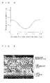
- Fig. 3 illustrates an example of distribution of the average grain diameter of crystal grains of the first semiconductor layer 3 in the thickness direction.
- the horizontal axis represents a distance from the lower electrode layer 2 and the vertical axis represents the average grain diameter of crystal grains.
- the second semiconductor layer 4 is a semiconductor layer of a second conductivity type which is different from the conductivity type of the first semiconductor layer 3.
- a photoelectric conversion layer with which charges are extracted well is formed.
- the first semiconductor layer 3 is a p-type
- the second semiconductor layer 4 is an n-type.
- the first semiconductor layer 3 may be an n-type and the second semiconductor layer 4 may be a p-type.
- a high-resistance buffer layer may be interposed between the first semiconductor layer 3 and the second semiconductor layer 4.
- Examples of the second semiconductor layer 4 include CdS, ZnS, ZnO, In 2 S 3 , In 2 Se 3 , In(OH, S), (Zn, In)(Se, OH), (Zn, Mg)O, and the like.
- the second semiconductor layer 4 is formed to have a thickness of 10 nm to 200 nm using, for example, a chemical bath deposition (CBD) method or the like.
- In (OH, S) means a mixed crystal compound containing In as a hydroxide and a sulfide.
- Zn, In)(Se, OH) is a mixed crystal compound containing Zn and In as a selenide and a hydroxide.
- (Zn,Mg) O is a compound containing Zn and Mg as an oxide.
- the upper electrode layer 5 may be further disposed on the second semiconductor layer 4.
- the upper electrode layer 5 is a layer with resistivity lower than that of the second semiconductor layer 4 and with which charges generated in the first semiconductor layer 3 and the second semiconductor layer 4 can be extracted well.
- the resistivity of the upper electrode layer 5 may be lower than 1 ⁇ cm and the sheet resistance thereof may be equal to or lower than 50 ⁇ / ⁇ .
- the upper electrode layer 5 is a transparent conductive film of 0.05 ⁇ m to 3 ⁇ m made of ITO or ZnO, or the like, for example.
- the upper electrode layer 5 may be formed of a semiconductor having the same conductivity type as that of the second semiconductor layer 4.
- the upper electrode layer 5 may be formed by a sputtering method, an evaporation method, a chemical vapor deposition (CVD) method, or the like.
- a collector electrode 8 may be further formed on the upper electrode layer 5.
- the collector electrode 8 is an electrode for further efficiently extracting charges generated in the first semiconductor layer 3 and the second semiconductor layer 4.
- the collector electrode 8 is formed, for example, linearly from one end of the photoelectric conversion cell 10 to the connection conductor 7 as illustrated in Fig. 1 . Accordingly, the current generated in the first semiconductor layer 3 and the fourth semiconductor layer 4 is collected in the collector electrode 8 through the upper electrode layer 5, and is efficiently passed to the adjacent photoelectric conversion cells 10 through the connection conductor 7.
- the collector electrode 8 may have a width of 50 ⁇ m to 400 ⁇ m from a viewpoint of improving light transmittance to the first semiconductor layer 3 and having good conductivity. Further, the collector electrode 8 may include a plurality of branched portions.
- the collector electrode 8 is formed by, for example, preparing a metal paste which is obtained by dispersing metal powder such as Ag powder in a resin binder or the like, printing the metal paste into a pattern shape, and curing the metal paste.
- connection conductor 7 is a conductor disposed in a groove penetrating the first semiconductor layer 3, the second semiconductor layer 4, and the second electrode layer 5.
- a metal, a conductive paste, or the like can be used for the connection conductor 7.
- the connection conductor 7 is formed by extending the collector electrode 8, but not limited thereto.
- the connection conductor 7 may be formed by extending the upper electrode layer 5.
- the photoelectric conversion device 11 having the above-described configuration
- the first semiconductor layer 3 is made of CIGS
- the lower electrode layer 2 which is formed of Mo or the like, is formed into a desired pattern using a sputtering method or the like on a main surface of the substrate 1 formed of glass or the like.
- a precursor layer which becomes the first semiconductor layer 3 is formed on the lower electrode layer 2 with a sputtering method, a coating method, or the like.
- the precursor layer may be a layer containing a raw material of a compound constituting the first semiconductor layer 3 or a layer containing fine grains of a compound constituting the first semiconductor layer 3.
- the precursor layer is subjected to a heat treatment at a temperature of 500°C to 600°C.
- a portion on the lower electrode layer 2 side of the precursor layer is subjected to active heat treatment by being irradiated with infrared light from the substrate 1 side using an IR lamp.
- the first semiconductor layer 3 whose average grain diameter is larger in the surface portion on the lower electrode layer 2 side than in the central portion in the thickness direction is formed.
- the second semiconductor layer 4 and the upper electrode layer 5 are sequentially formed on the first semiconductor layer 3 using a CBD method, a sputtering method, or the like.
- the first semiconductor layer 3, the second semiconductor layer 4, and the upper electrode layer 5 are processed through a mechanical scribing process or the like and consequently a groove for the connection conductor 7 is formed.
- conductive paste which is obtained by dispersing metal powder such as Ag powder in a resin binder or the like, is printed in a pattern shape on the upper electrode layer 5 and in the groove, and the collector electrode 8 and the connection conductor 7 are formed by heating and curing the printed conductive paste.
- the first semiconductor layer 3 to the collector electrode 8 are removed at a position shifted from the connection conductor 7 through a mechanical scribing process so as to provide a plurality of photoelectric conversion cells 10 being divided, thereby obtaining the photoelectric conversion device 11 illustrated in Figs. 1 and 2 .
- the average grain diameter of crystal grains in the first semiconductor layer 3 may be larger in the surface portion on the second semiconductor layer 4 side than in the central portion of the first semiconductor layer 3 in the thickness direction.
- recombination of charges at the grain boundaries can be suppressed in the surface portion on the second semiconductor layer 4 side. Consequently, the photoelectric conversion efficiency of the photoelectric conversion device 11 can be further improved.
- Fig. 4 illustrates distribution of the average grain diameter of crystal grains of the first semiconductor layer 3 in the thickness direction in the same manner as Fig. 3 .
- Such first semiconductor layer 3 becomes the first semiconductor layer 3 whose average grain diameter is larger in the surface portion on the second semiconductor layer 4 side than in the central portion in the thickness direction by being irradiated with the infrared light from the surface of the precursor layer opposite the lower electrode layer 2 using an IR lamp, when the above-described precursor layer is heated and consequently the first semiconductor layer 3 is formed.
- FIG. 5 is a cross section of the photoelectric conversion device 11 in which Mo is used for the lower electrode layer 2, CIGS is used for the first semiconductor layer 3, In(OH,S) is used for the second semiconductor layer 4 (because of the thinness, it is difficult to be confirmed in Fig. 5 ), and AZO is used for the transparent conductive film.
Landscapes
- Photovoltaic Devices (AREA)
Applications Claiming Priority (2)
| Application Number | Priority Date | Filing Date | Title |
|---|---|---|---|
| JP2012015095 | 2012-01-27 | ||
| PCT/JP2012/083510 WO2013111495A1 (fr) | 2012-01-27 | 2012-12-25 | Dispositif de conversion photoélectrique |
Publications (2)
| Publication Number | Publication Date |
|---|---|
| EP2808902A1 true EP2808902A1 (fr) | 2014-12-03 |
| EP2808902A4 EP2808902A4 (fr) | 2015-09-23 |
Family
ID=48873234
Family Applications (1)
| Application Number | Title | Priority Date | Filing Date |
|---|---|---|---|
| EP12866499.2A Withdrawn EP2808902A4 (fr) | 2012-01-27 | 2012-12-25 | Dispositif de conversion photoélectrique |
Country Status (4)
| Country | Link |
|---|---|
| US (1) | US9698288B2 (fr) |
| EP (1) | EP2808902A4 (fr) |
| JP (1) | JP5813139B2 (fr) |
| WO (1) | WO2013111495A1 (fr) |
Families Citing this family (1)
| Publication number | Priority date | Publication date | Assignee | Title |
|---|---|---|---|---|
| US9705018B2 (en) | 2012-11-20 | 2017-07-11 | Kabushiki Kaisha Toshiba | Photoelectric conversion element, method for manufacturing photoelectric conversion element, and solar cell |
Family Cites Families (9)
| Publication number | Priority date | Publication date | Assignee | Title |
|---|---|---|---|---|
| JPH07258881A (ja) | 1994-03-23 | 1995-10-09 | Yazaki Corp | CuInSe2 膜の製造方法 |
| JP2000299486A (ja) | 1999-04-12 | 2000-10-24 | Honda Motor Co Ltd | 太陽電池 |
| US20050056312A1 (en) * | 2003-03-14 | 2005-03-17 | Young David L. | Bifacial structure for tandem solar cells |
| US8106292B2 (en) * | 2007-04-30 | 2012-01-31 | Solyndra Llc | Volume compensation within a photovoltaic device |
| US8138410B2 (en) * | 2008-10-01 | 2012-03-20 | International Business Machines Corporation | Optical tandem photovoltaic cell panels |
| CN102318077B (zh) * | 2009-09-29 | 2013-08-14 | 京瓷株式会社 | 光电转换装置 |
| WO2011108033A1 (fr) | 2010-03-05 | 2011-09-09 | 株式会社 東芝 | Photopile en couches minces composite et son procédé de fabrication |
| JP2011249560A (ja) | 2010-05-27 | 2011-12-08 | Kyocera Corp | 半導体層の製造方法および光電変換装置の製造方法 |
| KR101807118B1 (ko) * | 2013-03-15 | 2017-12-08 | 나노코 테크놀로지스 리미티드 | 등급 크기 및 S:Se 비율을 갖는 광전 소자 |
-
2012
- 2012-12-25 WO PCT/JP2012/083510 patent/WO2013111495A1/fr not_active Ceased
- 2012-12-25 JP JP2013555163A patent/JP5813139B2/ja active Active
- 2012-12-25 EP EP12866499.2A patent/EP2808902A4/fr not_active Withdrawn
- 2012-12-25 US US14/375,126 patent/US9698288B2/en active Active
Also Published As
| Publication number | Publication date |
|---|---|
| US9698288B2 (en) | 2017-07-04 |
| JP5813139B2 (ja) | 2015-11-17 |
| JPWO2013111495A1 (ja) | 2015-05-11 |
| US20140366944A1 (en) | 2014-12-18 |
| EP2808902A4 (fr) | 2015-09-23 |
| WO2013111495A1 (fr) | 2013-08-01 |
Similar Documents
| Publication | Publication Date | Title |
|---|---|---|
| CN102576762A (zh) | 光伏系统及其制造方法 | |
| EP2565934B1 (fr) | Dispositif de conversion photoélectrique | |
| WO2012157449A1 (fr) | Dispositif à semi-conducteur, module de cellule solaire, chaîne de cellules solaires et réseau de cellules solaires | |
| EP3176831A1 (fr) | Dispositif de conversion photoélectrique, dispositif de conversion photoélectrique en tandem et réseau de dispositifs de conversion photoélectrique | |
| US9698288B2 (en) | Photoelectric conversion device | |
| US9184329B2 (en) | Photoelectric conversion device | |
| JP5860062B2 (ja) | 光電変換装置 | |
| JP2016103582A (ja) | 光電変換装置 | |
| JP2014067745A (ja) | 光電変換装置の製造方法 | |
| JP5705989B2 (ja) | 光電変換装置 | |
| JP2015176890A (ja) | 光電変換装置の製造方法 | |
| JP2014022562A (ja) | 光電変換装置の製造方法 | |
| JP2015122389A (ja) | 光電変換装置 | |
| JP2014049484A (ja) | 光電変換装置 | |
| JP2012156423A (ja) | 光電変換装置の製造方法 | |
| JP2012079769A (ja) | 光電変換装置 | |
| JP2014146659A (ja) | 光電変換装置 | |
| JP2014216332A (ja) | 光電変換装置 | |
| JP2014216419A (ja) | 光電変換装置 | |
| JP2014216420A (ja) | 光電変換装置 | |
| JP2013149650A (ja) | 光電変換装置 | |
| JP2014130982A (ja) | 光電変換装置 | |
| JP2014187215A (ja) | 光電変換装置 | |
| JP2013125813A (ja) | 光電変換装置の製造方法 | |
| JP2013125815A (ja) | 光電変換装置の製造方法 |
Legal Events
| Date | Code | Title | Description |
|---|---|---|---|
| PUAI | Public reference made under article 153(3) epc to a published international application that has entered the european phase |
Free format text: ORIGINAL CODE: 0009012 |
|
| 17P | Request for examination filed |
Effective date: 20140723 |
|
| AK | Designated contracting states |
Kind code of ref document: A1 Designated state(s): AL AT BE BG CH CY CZ DE DK EE ES FI FR GB GR HR HU IE IS IT LI LT LU LV MC MK MT NL NO PL PT RO RS SE SI SK SM TR |
|
| DAX | Request for extension of the european patent (deleted) | ||
| RA4 | Supplementary search report drawn up and despatched (corrected) |
Effective date: 20150826 |
|
| RIC1 | Information provided on ipc code assigned before grant |
Ipc: H01L 31/0392 20060101ALI20150820BHEP Ipc: H01L 31/032 20060101AFI20150820BHEP Ipc: H01L 31/0465 20140101ALI20150820BHEP Ipc: H01L 31/0368 20060101ALI20150820BHEP |
|
| STAA | Information on the status of an ep patent application or granted ep patent |
Free format text: STATUS: THE APPLICATION HAS BEEN WITHDRAWN |
|
| 18W | Application withdrawn |
Effective date: 20180919 |