EP2751809B1 - Memory refresh apparatuses - Google Patents
Memory refresh apparatuses Download PDFInfo
- Publication number
- EP2751809B1 EP2751809B1 EP12826784.6A EP12826784A EP2751809B1 EP 2751809 B1 EP2751809 B1 EP 2751809B1 EP 12826784 A EP12826784 A EP 12826784A EP 2751809 B1 EP2751809 B1 EP 2751809B1
- Authority
- EP
- European Patent Office
- Prior art keywords
- memory
- errors
- controller
- block
- refresh
- Prior art date
- Legal status (The legal status is an assumption and is not a legal conclusion. Google has not performed a legal analysis and makes no representation as to the accuracy of the status listed.)
- Active
Links
- 230000015654 memory Effects 0.000 title claims description 186
- 238000000034 method Methods 0.000 claims description 32
- 230000008672 reprogramming Effects 0.000 claims description 10
- 230000004044 response Effects 0.000 claims description 5
- 230000008569 process Effects 0.000 claims description 4
- 239000003550 marker Substances 0.000 claims 2
- 239000000758 substrate Substances 0.000 description 14
- 239000000463 material Substances 0.000 description 13
- 238000007667 floating Methods 0.000 description 7
- VYPSYNLAJGMNEJ-UHFFFAOYSA-N Silicium dioxide Chemical compound O=[Si]=O VYPSYNLAJGMNEJ-UHFFFAOYSA-N 0.000 description 5
- 230000001351 cycling effect Effects 0.000 description 3
- 238000010586 diagram Methods 0.000 description 3
- 239000003989 dielectric material Substances 0.000 description 3
- 239000002019 doping agent Substances 0.000 description 3
- 229910052814 silicon oxide Inorganic materials 0.000 description 3
- 230000005689 Fowler Nordheim tunneling Effects 0.000 description 2
- 230000008859 change Effects 0.000 description 2
- 239000004020 conductor Substances 0.000 description 2
- 238000013500 data storage Methods 0.000 description 2
- 230000000694 effects Effects 0.000 description 2
- 150000004767 nitrides Chemical class 0.000 description 2
- 239000004065 semiconductor Substances 0.000 description 2
- 229910052710 silicon Inorganic materials 0.000 description 2
- 239000010703 silicon Substances 0.000 description 2
- 230000001960 triggered effect Effects 0.000 description 2
- 230000005641 tunneling Effects 0.000 description 2
- ZOXJGFHDIHLPTG-UHFFFAOYSA-N Boron Chemical compound [B] ZOXJGFHDIHLPTG-UHFFFAOYSA-N 0.000 description 1
- GYHNNYVSQQEPJS-UHFFFAOYSA-N Gallium Chemical compound [Ga] GYHNNYVSQQEPJS-UHFFFAOYSA-N 0.000 description 1
- 238000009825 accumulation Methods 0.000 description 1
- 230000006978 adaptation Effects 0.000 description 1
- 229910052782 aluminium Inorganic materials 0.000 description 1
- XAGFODPZIPBFFR-UHFFFAOYSA-N aluminium Chemical compound [Al] XAGFODPZIPBFFR-UHFFFAOYSA-N 0.000 description 1
- 229910052787 antimony Inorganic materials 0.000 description 1
- WATWJIUSRGPENY-UHFFFAOYSA-N antimony atom Chemical compound [Sb] WATWJIUSRGPENY-UHFFFAOYSA-N 0.000 description 1
- 238000003491 array Methods 0.000 description 1
- 229910052785 arsenic Inorganic materials 0.000 description 1
- RQNWIZPPADIBDY-UHFFFAOYSA-N arsenic atom Chemical compound [As] RQNWIZPPADIBDY-UHFFFAOYSA-N 0.000 description 1
- 229910052796 boron Inorganic materials 0.000 description 1
- JJWKPURADFRFRB-UHFFFAOYSA-N carbonyl sulfide Chemical compound O=C=S JJWKPURADFRFRB-UHFFFAOYSA-N 0.000 description 1
- 230000001413 cellular effect Effects 0.000 description 1
- 230000008878 coupling Effects 0.000 description 1
- 238000010168 coupling process Methods 0.000 description 1
- 238000005859 coupling reaction Methods 0.000 description 1
- 230000005684 electric field Effects 0.000 description 1
- 238000005516 engineering process Methods 0.000 description 1
- 230000005669 field effect Effects 0.000 description 1
- 230000006870 function Effects 0.000 description 1
- 229910052733 gallium Inorganic materials 0.000 description 1
- BHEPBYXIRTUNPN-UHFFFAOYSA-N hydridophosphorus(.) (triplet) Chemical compound [PH] BHEPBYXIRTUNPN-UHFFFAOYSA-N 0.000 description 1
- 229910052738 indium Inorganic materials 0.000 description 1
- APFVFJFRJDLVQX-UHFFFAOYSA-N indium atom Chemical compound [In] APFVFJFRJDLVQX-UHFFFAOYSA-N 0.000 description 1
- 239000011810 insulating material Substances 0.000 description 1
- 239000012212 insulator Substances 0.000 description 1
- 238000002955 isolation Methods 0.000 description 1
- 230000007246 mechanism Effects 0.000 description 1
- 229910052751 metal Inorganic materials 0.000 description 1
- 239000002184 metal Substances 0.000 description 1
- 238000012544 monitoring process Methods 0.000 description 1
- 229910021420 polycrystalline silicon Inorganic materials 0.000 description 1
- 229920005591 polysilicon Polymers 0.000 description 1
- 230000004043 responsiveness Effects 0.000 description 1
- 235000012239 silicon dioxide Nutrition 0.000 description 1
- 239000000377 silicon dioxide Substances 0.000 description 1
- 239000007787 solid Substances 0.000 description 1
- 210000003813 thumb Anatomy 0.000 description 1
Images


Classifications
-
- G—PHYSICS
- G11—INFORMATION STORAGE
- G11C—STATIC STORES
- G11C16/00—Erasable programmable read-only memories
- G11C16/02—Erasable programmable read-only memories electrically programmable
- G11C16/06—Auxiliary circuits, e.g. for writing into memory
- G11C16/34—Determination of programming status, e.g. threshold voltage, overprogramming or underprogramming, retention
- G11C16/3418—Disturbance prevention or evaluation; Refreshing of disturbed memory data
-
- G—PHYSICS
- G06—COMPUTING; CALCULATING OR COUNTING
- G06F—ELECTRIC DIGITAL DATA PROCESSING
- G06F11/00—Error detection; Error correction; Monitoring
- G06F11/07—Responding to the occurrence of a fault, e.g. fault tolerance
- G06F11/0703—Error or fault processing not based on redundancy, i.e. by taking additional measures to deal with the error or fault not making use of redundancy in operation, in hardware, or in data representation
- G06F11/0706—Error or fault processing not based on redundancy, i.e. by taking additional measures to deal with the error or fault not making use of redundancy in operation, in hardware, or in data representation the processing taking place on a specific hardware platform or in a specific software environment
- G06F11/0727—Error or fault processing not based on redundancy, i.e. by taking additional measures to deal with the error or fault not making use of redundancy in operation, in hardware, or in data representation the processing taking place on a specific hardware platform or in a specific software environment in a storage system, e.g. in a DASD or network based storage system
-
- G—PHYSICS
- G06—COMPUTING; CALCULATING OR COUNTING
- G06F—ELECTRIC DIGITAL DATA PROCESSING
- G06F11/00—Error detection; Error correction; Monitoring
- G06F11/07—Responding to the occurrence of a fault, e.g. fault tolerance
- G06F11/0703—Error or fault processing not based on redundancy, i.e. by taking additional measures to deal with the error or fault not making use of redundancy in operation, in hardware, or in data representation
- G06F11/0706—Error or fault processing not based on redundancy, i.e. by taking additional measures to deal with the error or fault not making use of redundancy in operation, in hardware, or in data representation the processing taking place on a specific hardware platform or in a specific software environment
- G06F11/073—Error or fault processing not based on redundancy, i.e. by taking additional measures to deal with the error or fault not making use of redundancy in operation, in hardware, or in data representation the processing taking place on a specific hardware platform or in a specific software environment in a memory management context, e.g. virtual memory or cache management
-
- G—PHYSICS
- G06—COMPUTING; CALCULATING OR COUNTING
- G06F—ELECTRIC DIGITAL DATA PROCESSING
- G06F11/00—Error detection; Error correction; Monitoring
- G06F11/07—Responding to the occurrence of a fault, e.g. fault tolerance
- G06F11/0703—Error or fault processing not based on redundancy, i.e. by taking additional measures to deal with the error or fault not making use of redundancy in operation, in hardware, or in data representation
- G06F11/0751—Error or fault detection not based on redundancy
- G06F11/0754—Error or fault detection not based on redundancy by exceeding limits
- G06F11/076—Error or fault detection not based on redundancy by exceeding limits by exceeding a count or rate limit, e.g. word- or bit count limit
-
- G—PHYSICS
- G06—COMPUTING; CALCULATING OR COUNTING
- G06F—ELECTRIC DIGITAL DATA PROCESSING
- G06F11/00—Error detection; Error correction; Monitoring
- G06F11/07—Responding to the occurrence of a fault, e.g. fault tolerance
- G06F11/0703—Error or fault processing not based on redundancy, i.e. by taking additional measures to deal with the error or fault not making use of redundancy in operation, in hardware, or in data representation
- G06F11/0793—Remedial or corrective actions
-
- G—PHYSICS
- G06—COMPUTING; CALCULATING OR COUNTING
- G06F—ELECTRIC DIGITAL DATA PROCESSING
- G06F11/00—Error detection; Error correction; Monitoring
- G06F11/07—Responding to the occurrence of a fault, e.g. fault tolerance
- G06F11/08—Error detection or correction by redundancy in data representation, e.g. by using checking codes
- G06F11/10—Adding special bits or symbols to the coded information, e.g. parity check, casting out 9's or 11's
- G06F11/1008—Adding special bits or symbols to the coded information, e.g. parity check, casting out 9's or 11's in individual solid state devices
- G06F11/1048—Adding special bits or symbols to the coded information, e.g. parity check, casting out 9's or 11's in individual solid state devices using arrangements adapted for a specific error detection or correction feature
- G06F11/106—Correcting systematically all correctable errors, i.e. scrubbing
-
- G—PHYSICS
- G06—COMPUTING; CALCULATING OR COUNTING
- G06F—ELECTRIC DIGITAL DATA PROCESSING
- G06F11/00—Error detection; Error correction; Monitoring
- G06F11/07—Responding to the occurrence of a fault, e.g. fault tolerance
- G06F11/14—Error detection or correction of the data by redundancy in operation
- G06F11/1402—Saving, restoring, recovering or retrying
- G06F11/1415—Saving, restoring, recovering or retrying at system level
- G06F11/1417—Boot up procedures
-
- G—PHYSICS
- G11—INFORMATION STORAGE
- G11C—STATIC STORES
- G11C11/00—Digital stores characterised by the use of particular electric or magnetic storage elements; Storage elements therefor
- G11C11/56—Digital stores characterised by the use of particular electric or magnetic storage elements; Storage elements therefor using storage elements with more than two stable states represented by steps, e.g. of voltage, current, phase, frequency
-
- G—PHYSICS
- G11—INFORMATION STORAGE
- G11C—STATIC STORES
- G11C16/00—Erasable programmable read-only memories
- G11C16/02—Erasable programmable read-only memories electrically programmable
- G11C16/06—Auxiliary circuits, e.g. for writing into memory
- G11C16/26—Sensing or reading circuits; Data output circuits
Definitions
- a variety of computer systems and electronic devices use memory that is not volatile. In other words, the memory does not lose stored data when power is disconnected.
- These nonvolatile memories can be reprogrammed, read, and erased electronically, and are well-suited to store a variety of data such as music in digital audio players, pictures in digital cameras, and configuration data in cellular telephones.
- Such memory includes devices commonly known as flash memory, named in part because a flash operation is used to erase the content of a block of memory cells before it is reprogrammed. This type of memory is often packaged for consumer use in products such as CompactFlash memory cards, USB flash memory drives, and other such devices.
- Flash memory typically comprises a number of cells, each programmable to one of at least two data states, where each data state can represent a data value such as a digit (e.g, a bit) or digits of data.
- a typical flash memory cell comprises a field effect transistor having an electrically isolated charge storage structure such as a floating gate or charge trap that controls electrical conduction between source and drain regions of the memory cell. Data is represented by a charge stored on the charge storage structure, and the resulting change in conductivity observed between the source and drain regions.
- the charge storage structure separates a control gate from the source and drain regions of the memory cell. Electrons stored on the charge storage structure are electrically insulated from the control gate and the drain and source between adjacent data states becomes more difficult to accurately discern as the number of possible data states increases.
- US Patent Publication No. 2004/257888A1 to Noguchi et al. discloses a data storage system that determines whether a first page of data includes an error bit. When the data is determined to be an error bit, the first memory cell of the first page is erased and error corrected data is written.
- the invention is in the apparatus of Claim 1.
- Figure 1 illustrates an example nonvolatile memory cell.
- a source 101 and drain 102 are formed on a substrate 103, such as a p-type semiconductor material.
- the source 101, drain 102, and substrate 103 are in some embodiments formed of silicon, with a dopant having five valence electrons such as phosphorous, arsenic, or antimony to increase the electron concentration in the silicon or with a dopant having three valence electrons such as boron, gallium, indium, or aluminum to increase the hole concentration.
- Dopants are typically added in small, controlled quantities to produce the desired hole or electron concentration in the semiconductor material, resulting in n-type material if a surplus of electrons are present, such as in the source 101 and drain 102, and resulting in p-type material if an excess of holes are present such as in the substrate material 103.
- An insulator material such as silicon oxide (SiO2) is used to form an insulating layer 104, which has embedded within it a charge storage structure such as a floating gate 105, fabricated from a conductor such as metal or conductive polysilicon, or a charge trap (e.g., formed from a nitride material).
- a control gate 106 is similarly formed of a conductive material.
- the floating gate 105 is not directly electrically coupled to another conductive element of the memory cell, but is "floating" in the insulating material 104.
- the floating gate 105 is separated from the region of the p-type substrate material 103 between the source 101 and the drain 102 by a thin (e.g.
- a tunnel dielectric portion of the insulating layer 104 such as silicon dioxide (SiO2) and/or a combination of an oxide, a nitride, and an oxide (ONO).
- the charge storage structure 105 is able to store a charge due to its electrical isolation from other components of the memory cell.
- Programming or erasing a charge level on the charge storage structure 105 can be performed via a tunneling process known as Fowler-Nordheim tunneling, in which electrons tunnel through the portion of dielectric material 104 separating the charge storage structure 105 from the substrate 103.
- the portion o the dielectric material or materials separating the charge storage structure 105 from the substrate 103 are conventionally referred to as the tunnel dielectric.
- flash memory devices are categorized as either NOR flash or NAND flash, based on the arrangement of the memory cells or the circuitry used to perform read, program, and erase operations.
- the source 101 can be grounded and a supply voltage such as six volts can be applied to the drain 102.
- the drain voltage is applied via a bitline used to identify the memory cell to be programmed.
- a higher voltage such as 12 volts is also placed on the control gate 106 of the memory cell, forcing an inversion region to form in the p-type substrate due to the attraction of electrons to the positively charged control gate.
- the voltage difference between the source and drain in combination with the inversion region in the p-type material result in significant electron flow between the source 101 and drain 102 through the p-type substrate 103's inversion region, such that the kinetic energy of the electrons and the electric field generated by the control gate voltage at 106 result in Fowler-Nordheim tunneling of high-energy (also known as "hot") electrons across the tunnel dielectric and onto the charge storage structure 105.
- high-energy also known as "hot
- the charge storage structure thereby adopts a negative charge that counteracts any control gate positive charge's effect on the region of the substrate 103 between the source 101 and drain 102, raising the voltage that must be applied to the control gate 106 via a wordline to result in conduction across an inversion region in the p-type substrate material 103.
- the wordline's voltage is brought to a high voltage (such as five volts) during a read operation, the cell will not turn on due to the higher threshold voltage as a result of electrons stored on the charge storage structure 105 during the program operation.
- the read voltage applied to the control gate is larger than the threshold voltage Vt of an erased memory cell, but not large enough to allow conduction across an inversion region in the substrate 103 of a cell that has been programmed.
- the source 101 and drain 102 of the memory cell of Figure 1 can be grounded, and the control gate 106 can be brought to a voltage of perhaps 20 volts. This voltage is significantly higher than the 12 volt control gate voltage used to program the same memory cell using NOR flash methods, because a higher voltage makes up for the absence of "hot" electrons slowing between the source and drain of the memory cell.
- a similar tunneling of electrons can take place from the charge storage structure 105 to the source 101 of the memory cell.
- the source 101 is in some embodiments more deeply diffused than the drain to enhance erase performance.
- a positive voltage (such as twelve volts) can be applied to the source 101, the control gate 106 can be grounded, and the drain 102 can be left disconnected to perform an erase operation in one example.
- the large positive voltage on the source 101 attracts negatively charged electrons, causing them to tunnel through the insulating layer 104 and leave the floating gate 105. Because there is very little current flow between the source 101 and drain 102 during an erase operation, performing an erase operation takes very little current and consumes relatively little power.
- the source 101 and drain 102 can be left floating, but the substrate material 103 is brought to a high positive voltage (such as 20 volts), attracting the negatively charged electrons and causing them to tunnel from the charge storage structure 105 through the oxide insulating layer 104 to the substrate material 103.
- This method is sometimes known as "channel erase", because the channel region in substrate material 103 receives electrons from the charge storage structure 105.
- Memory cells such as that shown in Figure 1 can be arranged in arrays that are addressed via access lines known as wordlines, and data lines known as bitlines, as shown in Figure 2.
- Figure 2 shows a portion of a NAND flash memory array including a string of memory cells that can be selectively coupled to a single bitline, where each of the memory cells shown in the string is further selectable via a wordline 202.
- the string of memory cells 0-31 can be selectively coupled on the other side of the string to source line 203.
- the string can be coupled to (or isolated from) the bit line 201 and the source line 203 by operation of respective select transistors 204.
- the word line and therefore the control gate of the selected memory cell 202 can be maintained at a low but positive voltage level while the word lines of unselected memory cells can be brought to a sufficiently high voltage to cause the unselected memory cells to conduct irrespective of any charge that may be on the charge storage structures of the individual memory cells. If the selected memory cell has an uncharged charge storage structure it will conduct as a result of the low positive voltage level on the control gate, but if the charge storage structure has a negative charge it will raise the threshold voltage of the memory cell 202 above the low positive voltage applied to the control gate such that the cell does not conduct.
- the data state of the memory cell's charge storage structure can therefore be determined by, for example, monitoring conductivity or current flow between the bitline 201 and source line 203.
- the bitline 201 and source line 203 can be grounded via line select transistors 204 coupling the string to a grounded bitline 201 and source line 203.
- the gates of select transistors 204 are therefore again coupled to a voltage source such that the transistors conduct.
- the control gates of the memory cells not being programmed are brought to a sufficiently high voltage (e.g., ten volts) to inhibit inadvertent programming of those memory cells.
- the selected memory cell 202's control gate is coupled to a significantly higher voltage, such as 20 volts, such that electrons tunnel onto the charge storage structure.
- Strings of memory cells such as those of Figure 2 can be organized in blocks, such that a block is the smallest erasable unit of flash memory.
- Figure 3 shows a block of NAND flash memory, as may be used to practice some embodiments of the invention.
- 64 separate word lines shown at 301 provide 64 separately addressable physical pages of memory in the block, with each page capable of storing 4096 bytes of user data and 128 bytes of overhead data (sometimes referred to as spare bits), such as error correction code (ECC) data.
- ECC Data can be used to detect and/or correct some memory errors.
- the block can therefore store 256kB of user data plus 8 kB of overhead data.
- a conventional flash memory device contains many such blocks, for example a 1024 block memory device providing 256MB of user data storage.
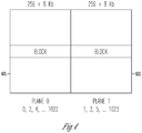
- FIG. 4 illustrates multiple planes of blocks such as the block shown in Figure 3 , as may be used to practice some embodiments of the invention.
- plane 0 as shown at 401 contains even-numbered blocks of memory
- plane 1 shown at 402 contains odd-numbered blocks of memory, for a total of 1024 blocks.
- Dividing the memory into two or more planes can provide faster memory operation, but may restrict memory operations to reading, programming, and erasing even and odd-numbered planes at the same time.
- an erase operation performed on block 0 of plane 0 could also include erasing block 1 of plane 1, and programming a page to block 1022 of plane 0 could result in also programming the corresponding page in block 1023 of plane 1.
- the programming operation and read operation are similar in that they involve applying a voltage to the memory cells being written in a write operation or non-selected cells in a memory cell string in a read operation
- multiple read, program, and/or erase operations can eventually affect the data state of a programmed memory cell.
- a conventional NAND flash memory can have the data states of its programmed memory cells corrupted after tens or hundreds of thousands of reads per page.
- a memory block of 64 pages as shown in Fig. 3 may have millions of read operations performed on the block to read the first 63 pages before the 64 th page is read, resulting in a significant chance of irrecoverable read errors on the 64 th page.
- Some embodiments of the invention therefore seek to reduce the occurrence of memory errors by refreshing the memory (e.g. copying and reprogramming) over time to prevent corruption or loss of the stored data.
- Refreshing the memory can be performed as a result of factors such as the passage of time since programming, exceeding a read error threshold, or powering on the memory device or memory controller (either directly, or indirectly such as by powering on a memory controller coupled to the memory device).
- a memory controller reads through memory systematically to detect blocks with levels of memory errors that exceed a certain threshold, and refreshes the blocks before the errors become irrecoverable. Because it can be desirable to limit the number of times a memory cell is programmed, unnecessary programming can be avoided by not refreshing data if the minimum error threshold is not exceeded. For example, if error correction data enables correction of 24 bits in a page, a block might only be refreshed if half of the correctable bits (12 bits in this example) are found to be in error in a page read operation performed on the block.
- Some devices such as portable game systems, smart phones, portable media devices, and other such devices are power cycled (i.e. powered on and powered off) relatively frequently, reducing the ability of the device to scan through all memory and manage potential read errors effectively.
- Some embodiments of the invention therefore use power cycling to manage errors in a nonvolatile memory, such as by using power cycles to trigger memory scan and refresh operations and performing these operations on a fine-grained level.
- the impact of a single memory scan and refresh operation can be minimized in one example by scanning and refreshing on a block level, such that copying and reprgramming of perhaps megabytes of data stored in a single block can be completed in, for example, hundreds of milliseconds.
- at least one different block is scanned in response to each power on, ensuring that blocks of memory are scanned and refreshed if needed on a regular basis.
- the device restart process in one example includes determining whether a block of memory from the device is already marked for refresh (e.g. such as when refreshing a block marked for refresh was not completed before power was lost). This method can be supplemented by a tracking mechanism in a further example, which tracks reads performed on each block and checks several pages of the block for errors periodically (e.g. every thousand reads).
- nonvolatile memory such as in a register or in a portion of the memory array itself, and can be used to ensure that block checks triggered by power cycling or performed as a background task proceed through all of the memory rather than restarting at the same block for each power cycle. Refreshing can be further tracked across power cycling by marking blocks for refresh, such that queued or incomplete block refreshes can be completed as part of a power on sequence or during device operation after a power on sequence completes.
- nonvolatile memory can also store the number of page reads per device or block, enabling a device that reboots frequently to count accumulated read operations across power cycles rather than lose count of page reads when a device is powered off.
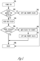
- FIG. 5 is a flowchart illustrating a method of managing memory errors triggered by a power on sequence, consistent with an example embodiment of the invention.
- a device is powered on and starts a power-on sequence, including determining whether any blocks of memory are already marked for refresh, such as by checking a nonvolatile memory location (e.g., a register) for block information, or by checking flags associated with memory blocks. If a memory block is marked in some way for refresh at 502, the data stored in the block is copied and reprogrammed at 503.
- a nonvolatile memory location e.g., a register
- an identified block of memory is read at 504.
- the memory block is identified by looking up a pointer to a next unchecked memory block in a power cycle-based memory refresh, so that the method proceeds through memory across power cycles rather than restarting with the same memory block at each power on sequence.
- the number of errors per page are counted using ECC, and it is determined whether the number of errors exceed a threshold at 505.
- a memory that can correct up to 24 bits per page using stored ECC data exceeds its acceptable number of errors if 12 bits (e.g. approximately half the correctable number of bits) in any page of the block are in error and need to be corrected.
- Other thresholds such as one third the number of correctable bits, can be used in other embodiments. Thresholds can vary based on factors such as the number of operations implemented in the life of the memory, or the age of the memory.
- the block is marked for refresh at 506.
- the data of the block is then copied, error correction code data is used to fix the correctable errors, and the data is reprogrammed at 507.
- the block can be marked for refresh before copying and reprogramming so that if the device is powered off or the method is otherwise interrupted before copying and reprogramming can complete at 507, the data of the block will still be copied and reprogrammed (such as at 502 and 503) when the device is powered on again.
- the flag marking the block for refresh at 506 is therefore not cleared in this example until the copying and reprogramming at 507 are complete.
- the memory is ready for normal operation.
- the copying and reprogramming at 503 that is performed if a memory block is marked for refresh on power on does not result in a ready state when complete, but instead proceeds to 504 where at least one new block is read before the memory device becomes ready, which can ensure that at least one new block is read on each normal power cycle.
- the method illustrated in Figure 5 can be used to ensure that at least one block is checked or refreshed on each power cycle, but can be configured such that only one block will be refreshed as part of the power on cycle.
- reading a typical block currently takes on the order of a millisecond using some technologies reprogramming the block can currently take on the order of hundreds of milliseconds, so reprogramming several blocks could significantly delay memory availability during the power on sequence.
- Some standards such as the JEDEC Flash Memory standards require that memory be ready for operation within a certain time period after power on, such as within one second. For this reason, some embodiments such as the example shown in Figure 5 can limit the number of programming operations that occur as part of the device startup method, such as by ensuring that only one block is reprogrammed before the memory becomes ready for regular access operations.
- a read is performed after receiving a read command, at 601, and a read counter is updated at 602 (e.g., by incrementing an up-counter or decrementing a down-counter). Because a read command can result in multiple pages being read, the counter can count a number of pages read rather than read commands, such as to ensure that an accurate count of the number of times a page has been read can be maintained.
- a threshold e.g. the number of page reads reaches 1024 pages as illustrated at 603
- a particular number of pages (e.g. 16 pages) of a block of memory identified by a refresh block pointer are read and checked for errors at 604.
- other suitable read thresholds and numbers of pages to be read will be used.
- the block identified by the refresh block pointer is marked for refresh at 606.
- the data of the block is then read and copied (e.g., into a buffer memory) for reprogramming (e.g., page by page) as shown at 607, such as to update the data stored in memory with corrected and freshly programmed data.
- the flag indicating the block is to be reprogrammed is cleared. The block copy and reprogram can therefore be repeated at the next power cycle if it does not complete successfully before the next power cycle occurs, as the flag indicating the block is to be reprogrammed will still be set.
- the background refresh method then continues at 608, with the page read counter being reset (e.g., to zero).
- the threshold of pages read can be based on factors such as read disturb testing on a particular memory configuration, memory device density, and other such factors.
- the data of the block is relocated to another block location in physical memory as part of a wear-leveling method, reducing further wear on a physical block of memory already determined to have an unacceptable read error rate.
- the block refresh method at 606-607 in this example completes before further refresh scan reads occur at 604, to prevent accumulation of blocks marked for refresh.
- the method illustrated in Figure 6 operates such that only one block at the most is marked for refresh at any one time.
- the current block and page being read as part of the refresh scan method are stored in memory, which in some embodiments comprises a nonvolatile memory.
- the memory location of the background refresh method is therefore not lost during a power cycle.
- only the block location of the background refresh method is stored in nonvolatile memory as it is updated relatively infrequently, and the page location pointing to the particular 16 pages of the block to scan, as reflected at 604, is stored in volatile memory (such as random access memory or RAM).
- volatile memory such as random access memory or RAM
- Error threshold level, rate of refresh, and other such parameters can be selected in a further embodiment to avoid under-refresh or over-refresh of the device. Although it is often undesirable to allow errors to accumulate to the point where an uncorrectable read error may occur, it is also often undesirable to refresh nonvolatile memory too frequently, as unnecessary wear on the nonvolatile memory cells can result in, for example, a shortened lifespan of the memory device.
- the rate of refresh can also be chosen to reduce the chances of an uncorrectable read disturb error occurring before a page can be refreshed.
- a nonvolatile memory having 1024 total blocks and 256 pages per block. If 100,000 reads per page in a block are needed for a read disturb in that block to become reasonably possible, 100,000 reads per page times 256 pages per block results in approximately 26 million reads in the block for a read disturb event to become reasonably possible. 26 million reads per block divided by 1024 blocks suggests that one block should be refreshed every 26,000 page reads to make a read disturb error reasonably unlikely. Refreshing at a faster rate, such as one block every 16,000 page reads provides some extra margin of safety.
- Reading an entire block at one time as part of a background refresh method can currently take about 100 milliseconds, which may be acceptable at power-on but undesirable during operation. Reading a single page at a time for a refresh scan can currently take about a millisecond, but might be performed every 64 user page reads in the above example with one block refreshed per 16,000 user page reads. Similarly, reading 16 pages for a refresh scan currently takes approximately 8 milliseconds, and might be performed every 1024 user page reads to refresh an entire block every 16,000 user page reads.
- Reading and programming a block currently takes approximately 500 milliseconds, so the combined total time to read a block to check for errors and then read and reprogram the block in this example is approximately 600 milliseconds. If 16 pages are read for a refresh scan every 1024 user page reads, the total impact on the user would be approximately 8ms delay every 1024 pages read, plus approximately 2-3ms to update the active block address in nonvolatile memory as scanning each block is completed. In the rare event a refresh is needed, an additional 500ms delay will occur to copy and reprogram the block. As this is expected to be an uncommon occurrence in most real-world applications and is preferable to an irrecoverable read-induced memory error, the half-second delay should be acceptable for most applications.
- the refresh of the block can be split into multiple operations. For example, 16 operations of reprogramming 16 pages will copy a 256 page block over time, while causing only about a 32ms delay maximum to any one system memory access.
- the memory device may allow for a normal memory access to interrupt a block copy, perform the normal access, and then resume the copy to provide minimum delay to normal operations.
- the refresh methods described herein in some embodiments are managed by a memory controller that is integral to a memory device, such as one that forms a part of a flash memory card, and in other embodiments are implemented external to a memory device, such that the methods described above can be employed with off-the-shelf nonvolatile memory devices.
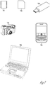
- Figure 7 shows a variety of devices operable to employ methods such as those described herein.
- a nonvolatile memory integrated circuit such as a flash memory integrated circuit.
- the integrated circuit includes an integral controller, while in other embodiments an external memory controller performs memory refresh operations.
- a flash memory card is similarly shown at 702 (e.g., a secure digital (SD) memory card), which again may include an integral controller or may be refreshed by an external controller (e.g., as embodied in hardware, firmware, and/or software).
- SD secure digital
- a flash memory drive often known as a thumb drive or USB flash drive is shown at 703, often employing large amounts of portable, nonvolatile memory ranging into tens of gigabytes and more. Consumers often use such drives to store and carry data between computers, such as saved documents, multimedia files, and the like.
- a digital camera is shown at 704, which often includes both internal flash memory for storing firmware and other data as well as a flash memory card (such as shown at 702) for storing photographs, video, and other data.
- Refresh methods such as those described herein are also useful in smart phones, portable gaming systems, personal digital assistants (PDAs), or other such devices as shown at 705.
- PDAs personal digital assistants
- These devices use nonvolatile memory such as flash memory to store programs and other data.
- Nonvolatile memory is also becoming increasingly common as a high-performance option in personal computers as shown at 706, both for storing data such as firmware and configuration data, as well as in solid-state drives (SSD). Because solid-state drives outperform typical hard disk drives by a significant margin, use of solid state drives can improve computer responsiveness and speed, making tasks such as booting, launching an application, or restoring from a hibernate state much quicker for the end user.
Applications Claiming Priority (2)
| Application Number | Priority Date | Filing Date | Title |
|---|---|---|---|
| US13/222,282 US9176800B2 (en) | 2011-08-31 | 2011-08-31 | Memory refresh methods and apparatuses |
| PCT/US2012/052687 WO2013033107A2 (en) | 2011-08-31 | 2012-08-28 | Memory refresh methods and apparatuses |
Publications (3)
| Publication Number | Publication Date |
|---|---|
| EP2751809A2 EP2751809A2 (en) | 2014-07-09 |
| EP2751809A4 EP2751809A4 (en) | 2014-12-31 |
| EP2751809B1 true EP2751809B1 (en) | 2020-04-01 |
Family
ID=47745458
Family Applications (1)
| Application Number | Title | Priority Date | Filing Date |
|---|---|---|---|
| EP12826784.6A Active EP2751809B1 (en) | 2011-08-31 | 2012-08-28 | Memory refresh apparatuses |
Country Status (6)
| Country | Link |
|---|---|
| US (3) | US9176800B2 (zh) |
| EP (1) | EP2751809B1 (zh) |
| JP (1) | JP5901771B2 (zh) |
| KR (1) | KR102000307B1 (zh) |
| CN (2) | CN103843069B (zh) |
| WO (1) | WO2013033107A2 (zh) |
Families Citing this family (50)
| Publication number | Priority date | Publication date | Assignee | Title |
|---|---|---|---|---|
| US9176800B2 (en) | 2011-08-31 | 2015-11-03 | Micron Technology, Inc. | Memory refresh methods and apparatuses |
| US9256526B2 (en) * | 2012-02-23 | 2016-02-09 | National Taiwan University | Flash memory storage system and access method |
| US9430735B1 (en) | 2012-02-23 | 2016-08-30 | Micron Technology, Inc. | Neural network in a memory device |
| KR102025193B1 (ko) * | 2013-02-19 | 2019-09-25 | 삼성전자주식회사 | 메모리 컨트롤러 및 그것의 동작 방법, 메모리 컨트롤러를 포함하는 메모리 시스템 |
| JP2014241057A (ja) * | 2013-06-12 | 2014-12-25 | ソニー株式会社 | インターフェース制御回路、メモリシステム、および、インターフェース制御回路の制御方法 |
| TWI490870B (zh) * | 2013-08-06 | 2015-07-01 | Silicon Motion Inc | 資料儲存裝置及其資料維護方法 |
| CN104346236B (zh) | 2013-08-06 | 2018-03-23 | 慧荣科技股份有限公司 | 数据储存装置及其数据维护方法 |
| JP6270377B2 (ja) * | 2013-08-27 | 2018-01-31 | キヤノン株式会社 | 画像形成装置 |
| CN104978998B (zh) * | 2014-04-01 | 2019-05-31 | 北京兆易创新科技股份有限公司 | 一种非易失存储器的处理方法及装置 |
| DE102014104717B4 (de) * | 2014-04-03 | 2019-08-01 | Hyperstone Gmbh | Verfahren und Vorrichtung zur Datenerneuerung für eine Erhöhung der Zuverlässigkeit von Flashspeichern |
| JP6226830B2 (ja) * | 2014-07-24 | 2017-11-08 | 株式会社東芝 | 情報処理装置、データアクセス方法およびプログラム |
| CN105374389B (zh) * | 2014-08-07 | 2018-09-07 | 华邦电子股份有限公司 | 存储器电路及其刷新方法 |
| KR20160042224A (ko) | 2014-10-07 | 2016-04-19 | 에스케이하이닉스 주식회사 | 데이터 저장 장치 및 그것의 동작 방법 |
| US9678827B2 (en) * | 2014-10-07 | 2017-06-13 | SK Hynix Inc. | Access counts for performing data inspection operations in data storage device |
| US9552171B2 (en) * | 2014-10-29 | 2017-01-24 | Sandisk Technologies Llc | Read scrub with adaptive counter management |
| KR20160063726A (ko) * | 2014-11-27 | 2016-06-07 | 에스케이하이닉스 주식회사 | 메모리 장치 및 이를 포함하는 메모리 시스템 |
| US9595342B2 (en) * | 2015-01-20 | 2017-03-14 | Sandisk Technologies Llc | Method and apparatus for refresh programming of memory cells based on amount of threshold voltage downshift |
| KR102277521B1 (ko) * | 2015-01-23 | 2021-07-16 | 삼성전자주식회사 | 저장 장치 및 그것의 리드 리클레임 및 읽기 방법 |
| US9558064B2 (en) * | 2015-01-28 | 2017-01-31 | Micron Technology, Inc. | Estimating an error rate associated with memory |
| KR20160110774A (ko) | 2015-03-12 | 2016-09-22 | 에스케이하이닉스 주식회사 | 메모리 장치 및 이를 포함하는 시스템 |
| US9772901B2 (en) * | 2015-05-08 | 2017-09-26 | Nxp Usa, Inc. | Memory reliability using error-correcting code |
| US9852795B2 (en) | 2015-09-24 | 2017-12-26 | Samsung Electronics Co., Ltd. | Methods of operating nonvolatile memory devices, and memory systems including nonvolatile memory devices |
| KR102359979B1 (ko) | 2015-11-16 | 2022-02-08 | 삼성전자주식회사 | 솔리드 스테이트 드라이브 장치 및 이를 포함하는 저장 시스템 |
| US11481126B2 (en) * | 2016-05-24 | 2022-10-25 | Micron Technology, Inc. | Memory device error based adaptive refresh rate systems and methods |
| US10248499B2 (en) * | 2016-06-24 | 2019-04-02 | Sandisk Technologies Llc | Non-volatile storage system using two pass programming with bit error control |
| US9747158B1 (en) * | 2017-01-13 | 2017-08-29 | Pure Storage, Inc. | Intelligent refresh of 3D NAND |
| US11955187B2 (en) * | 2017-01-13 | 2024-04-09 | Pure Storage, Inc. | Refresh of differing capacity NAND |
| KR20180092422A (ko) * | 2017-02-09 | 2018-08-20 | 에스케이하이닉스 주식회사 | 데이터 저장 장치 및 그것의 동작 방법 |
| US10019332B1 (en) * | 2017-03-10 | 2018-07-10 | Western Digital Technologies, Inc. | Non-volatile memory with program failure recovery |
| KR101985309B1 (ko) | 2017-06-12 | 2019-06-04 | 주식회사 티맥스데이터 | 최적화된 높이를 가지는 밸런스드 파스 트리를 생성하는 방법 |
| CN109215715B (zh) * | 2017-07-05 | 2020-06-26 | 中国科学院微电子研究所 | 一种闪存存储电路的抗总剂量辐照加固方法 |
| US10140042B1 (en) | 2017-09-13 | 2018-11-27 | Toshiba Memory Corporation | Deterministic read disturb counter-based data checking for NAND flash |
| KR20200067848A (ko) | 2017-09-30 | 2020-06-12 | 마이크론 테크놀로지, 인크. | 우선적 유휴 시간 판독 스캔 |
| US10269445B1 (en) * | 2017-10-22 | 2019-04-23 | Nanya Technology Corporation | Memory device and operating method thereof |
| TWI646535B (zh) * | 2017-12-27 | 2019-01-01 | 慧榮科技股份有限公司 | 資料儲存裝置以及非揮發式記憶體操作方法 |
| CN108564981B (zh) * | 2018-03-27 | 2021-10-01 | 深圳忆联信息系统有限公司 | 一种存储装置数据安全动态监控方法 |
| US11245583B2 (en) * | 2018-05-03 | 2022-02-08 | Micron Technology, Inc. | Determining whether a vehicle should be configured for a different region |
| KR20200079851A (ko) * | 2018-12-26 | 2020-07-06 | 에스케이하이닉스 주식회사 | 메모리 시스템 및 그것의 동작방법 |
| KR20200087557A (ko) * | 2019-01-11 | 2020-07-21 | 주식회사 엘지화학 | 에러 복구 방법, 이를 이용한 마이크로 컨트롤러 유닛, 및 상기 마이크로 컨트롤러를 포함하는 배터리 장치 |
| US10867654B2 (en) * | 2019-01-17 | 2020-12-15 | Xerox Corporation | Method for testing a memory device |
| US11004534B2 (en) * | 2019-08-06 | 2021-05-11 | Micron Technology, Inc. | Preemptive read refresh in memories with time-varying error rates |
| JP2021071776A (ja) | 2019-10-29 | 2021-05-06 | キオクシア株式会社 | メモリシステム |
| US11200113B2 (en) * | 2020-01-14 | 2021-12-14 | Intel Corporation | Auto-increment write count for nonvolatile memory |
| KR20210100790A (ko) | 2020-02-06 | 2021-08-18 | 삼성전자주식회사 | 스토리지 장치 및 스토리지 장치의 동작 방법 |
| US11809743B2 (en) | 2020-09-21 | 2023-11-07 | Advanced Micro Devices, Inc. | Refresh management list for DRAM |
| US11461025B2 (en) * | 2020-11-05 | 2022-10-04 | Macronix International Co., Ltd. | Data retention in memory devices |
| CN112634978A (zh) * | 2020-12-23 | 2021-04-09 | 江苏国科微电子有限公司 | 一种NVMe固态硬盘异常处理方法、装置及集成芯片 |
| US11914887B2 (en) * | 2021-04-14 | 2024-02-27 | Macronix International Co., Ltd. | Storage device and data accessing method using multi-level cell |
| US11500578B2 (en) | 2021-04-19 | 2022-11-15 | Micron Technology, Inc. | Memory access threshold based memory management |
| US20220404968A1 (en) * | 2021-06-18 | 2022-12-22 | Micron Technology, Inc. | Read performance techniques for time retention |
Family Cites Families (34)
| Publication number | Priority date | Publication date | Assignee | Title |
|---|---|---|---|---|
| JPS6022438B2 (ja) * | 1980-05-06 | 1985-06-01 | 松下電器産業株式会社 | 不揮発性メモリのリフレッシュ方式 |
| JP2892590B2 (ja) | 1994-07-15 | 1999-05-17 | 秀信 甕 | 土瓦塀風囲い用支持ブロック |
| JP3176019B2 (ja) * | 1995-04-05 | 2001-06-11 | 株式会社東芝 | 不揮発性半導体記憶部を含む記憶システム |
| JPH09204367A (ja) | 1996-01-25 | 1997-08-05 | Mitsubishi Electric Corp | フラッシュディスクカードにおけるフラッシュメモリデータのリフレッシュ方法 |
| US5909449A (en) | 1997-09-08 | 1999-06-01 | Invox Technology | Multibit-per-cell non-volatile memory with error detection and correction |
| US7035155B2 (en) | 2002-09-26 | 2006-04-25 | Xware Technology, Inc. | Dynamic memory management |
| JP2004259144A (ja) | 2003-02-27 | 2004-09-16 | Renesas Technology Corp | 半導体記憶装置 |
| JP4256198B2 (ja) * | 2003-04-22 | 2009-04-22 | 株式会社東芝 | データ記憶システム |
| US7321951B2 (en) * | 2003-11-17 | 2008-01-22 | Micron Technology, Inc. | Method for testing flash memory power loss recovery |
| US20070204107A1 (en) * | 2004-02-24 | 2007-08-30 | Analog Devices, Inc. | Cache memory background preprocessing |
| US7325090B2 (en) | 2004-04-29 | 2008-01-29 | Sandisk Il Ltd. | Refreshing data stored in a flash memory |
| KR100802059B1 (ko) | 2006-09-06 | 2008-02-12 | 삼성전자주식회사 | 읽기 디스터브로 인한 배드 블록의 생성을 억제할 수 있는메모리 시스템 및 그것의 동작 방법 |
| JP2008090778A (ja) | 2006-10-05 | 2008-04-17 | Matsushita Electric Ind Co Ltd | 不揮発性メモリ用メモリコントローラ、不揮発性記憶装置、不揮発性記憶システム、不揮発性メモリのメモリ制御方法 |
| US7894289B2 (en) * | 2006-10-11 | 2011-02-22 | Micron Technology, Inc. | Memory system and method using partial ECC to achieve low power refresh and fast access to data |
| US7840837B2 (en) * | 2007-04-27 | 2010-11-23 | Netapp, Inc. | System and method for protecting memory during system initialization |
| KR101043013B1 (ko) * | 2007-07-18 | 2011-06-21 | 후지쯔 가부시끼가이샤 | 메모리 리프레시 장치 및 메모리 리프레시 방법 |
| US8060798B2 (en) | 2007-07-19 | 2011-11-15 | Micron Technology, Inc. | Refresh of non-volatile memory cells based on fatigue conditions |
| US7937647B2 (en) * | 2007-07-27 | 2011-05-03 | Actel Corporation | Error-detecting and correcting FPGA architecture |
| US7770079B2 (en) | 2007-08-22 | 2010-08-03 | Micron Technology Inc. | Error scanning in flash memory |
| JP2009087509A (ja) | 2007-10-03 | 2009-04-23 | Toshiba Corp | 半導体記憶装置 |
| US8499229B2 (en) * | 2007-11-21 | 2013-07-30 | Micro Technology, Inc. | Method and apparatus for reading data from flash memory |
| US8161356B2 (en) * | 2008-03-28 | 2012-04-17 | Intel Corporation | Systems, methods, and apparatuses to save memory self-refresh power |
| JP4267682B1 (ja) | 2008-06-04 | 2009-05-27 | 株式会社ハギワラシスコム | Nandフラッシュメモリのリフレッシュ方法 |
| US20090327581A1 (en) | 2008-06-30 | 2009-12-31 | Coulson Richard L | Nand memory |
| JP2010067010A (ja) | 2008-09-11 | 2010-03-25 | Fuji Electric Systems Co Ltd | 組み込み機器、不揮発性メモリの自動リフレッシュ方法およびプログラム |
| US8982653B2 (en) | 2008-11-11 | 2015-03-17 | Memory Technologies Llc | Method and device for temperature-based data refresh in non-volatile memories |
| US8281229B2 (en) | 2008-12-30 | 2012-10-02 | Intel Corporation | Firmware verification using system memory error check logic |
| US8248831B2 (en) | 2008-12-31 | 2012-08-21 | Apple Inc. | Rejuvenation of analog memory cells |
| JP5185156B2 (ja) * | 2009-02-24 | 2013-04-17 | 株式会社東芝 | メモリコントローラおよび半導体記憶装置 |
| KR20110026578A (ko) | 2009-09-08 | 2011-03-16 | 엘지전자 주식회사 | 시스템 메모리의 에러 보정 장치 및 방법 |
| JP2011107851A (ja) * | 2009-11-13 | 2011-06-02 | Toshiba Corp | メモリシステム |
| JP2011128751A (ja) | 2009-12-16 | 2011-06-30 | Clarion Co Ltd | データ記録装置およびデータ記録装置の制御方法 |
| US8756474B2 (en) * | 2011-03-21 | 2014-06-17 | Denso International America, Inc. | Method for initiating a refresh operation in a solid-state nonvolatile memory device |
| US9176800B2 (en) | 2011-08-31 | 2015-11-03 | Micron Technology, Inc. | Memory refresh methods and apparatuses |
-
2011
- 2011-08-31 US US13/222,282 patent/US9176800B2/en active Active
-
2012
- 2012-08-28 JP JP2014528524A patent/JP5901771B2/ja active Active
- 2012-08-28 EP EP12826784.6A patent/EP2751809B1/en active Active
- 2012-08-28 WO PCT/US2012/052687 patent/WO2013033107A2/en active Application Filing
- 2012-08-28 CN CN201280048444.1A patent/CN103843069B/zh active Active
- 2012-08-28 CN CN201710470081.5A patent/CN107402832B/zh active Active
- 2012-08-28 KR KR1020147007711A patent/KR102000307B1/ko active IP Right Grant
-
2015
- 2015-09-28 US US14/867,985 patent/US10109357B2/en active Active
-
2017
- 2017-08-23 US US15/684,763 patent/US10290359B2/en active Active
Non-Patent Citations (1)
| Title |
|---|
| None * |
Also Published As
| Publication number | Publication date |
|---|---|
| JP2014525634A (ja) | 2014-09-29 |
| US20160019974A1 (en) | 2016-01-21 |
| CN107402832A (zh) | 2017-11-28 |
| US9176800B2 (en) | 2015-11-03 |
| US10290359B2 (en) | 2019-05-14 |
| US10109357B2 (en) | 2018-10-23 |
| EP2751809A2 (en) | 2014-07-09 |
| EP2751809A4 (en) | 2014-12-31 |
| US20170352429A1 (en) | 2017-12-07 |
| CN103843069A (zh) | 2014-06-04 |
| CN107402832B (zh) | 2020-11-27 |
| WO2013033107A2 (en) | 2013-03-07 |
| KR20140059821A (ko) | 2014-05-16 |
| US20130055046A1 (en) | 2013-02-28 |
| CN103843069B (zh) | 2017-07-11 |
| WO2013033107A3 (en) | 2013-04-25 |
| KR102000307B1 (ko) | 2019-07-15 |
| JP5901771B2 (ja) | 2016-04-13 |
Similar Documents
| Publication | Publication Date | Title |
|---|---|---|
| US10290359B2 (en) | Memory refresh methods and apparatuses | |
| US8971119B2 (en) | Select transistor tuning | |
| TWI321795B (en) | Methods for operating memory integrated circuit and reading data stored as levels of charge in a plurality of reprogrammable non-volatile memory cells, stotage device, and memory system | |
| EP2154687B1 (en) | Erased sector detection mechanisms | |
| US9026757B2 (en) | Non-volatile memory programming data preservation | |
| US9070449B2 (en) | Defective block management | |
| US10680005B2 (en) | Nonvolatile memory device, method of operating nonvolatile memory device and storage device including the same | |
| US9983916B2 (en) | Memory system and operating method thereof | |
| CN105551521B (zh) | 存储系统及其操作方法 | |
| US9384845B2 (en) | Partial erase of nonvolatile memory blocks | |
| EP2948956B1 (en) | Recovery of nearby data in programming of non-volatile multi-level multiple memory die | |
| EP2179362B1 (en) | Memory system | |
| US9152497B2 (en) | Data recovery from blocks with gate shorts | |
| US8804424B2 (en) | Memory with three transistor memory cell device | |
| US11538535B2 (en) | Apparatus for rapid data destruction | |
| CN109254723B (zh) | 非易失性存储器中的存储器扇区注销的方法和系统 | |
| CN114631080A (zh) | 用于存储器的数据恢复管理 | |
| CN115705908A (zh) | 存储设置数据的存储器件及其操作方法 |
Legal Events
| Date | Code | Title | Description |
|---|---|---|---|
| PUAI | Public reference made under article 153(3) epc to a published international application that has entered the european phase |
Free format text: ORIGINAL CODE: 0009012 |
|
| 17P | Request for examination filed |
Effective date: 20140324 |
|
| AK | Designated contracting states |
Kind code of ref document: A2 Designated state(s): AL AT BE BG CH CY CZ DE DK EE ES FI FR GB GR HR HU IE IS IT LI LT LU LV MC MK MT NL NO PL PT RO RS SE SI SK SM TR |
|
| DAX | Request for extension of the european patent (deleted) | ||
| A4 | Supplementary search report drawn up and despatched |
Effective date: 20141127 |
|
| RIC1 | Information provided on ipc code assigned before grant |
Ipc: G06F 11/10 20060101ALI20141121BHEP Ipc: G11C 16/00 20060101ALI20141121BHEP Ipc: G11C 29/42 20060101AFI20141121BHEP Ipc: G11C 16/02 20060101ALI20141121BHEP |
|
| STAA | Information on the status of an ep patent application or granted ep patent |
Free format text: STATUS: EXAMINATION IS IN PROGRESS |
|
| 17Q | First examination report despatched |
Effective date: 20180515 |
|
| GRAP | Despatch of communication of intention to grant a patent |
Free format text: ORIGINAL CODE: EPIDOSNIGR1 |
|
| STAA | Information on the status of an ep patent application or granted ep patent |
Free format text: STATUS: GRANT OF PATENT IS INTENDED |
|
| INTG | Intention to grant announced |
Effective date: 20191010 |
|
| GRAS | Grant fee paid |
Free format text: ORIGINAL CODE: EPIDOSNIGR3 |
|
| GRAA | (expected) grant |
Free format text: ORIGINAL CODE: 0009210 |
|
| STAA | Information on the status of an ep patent application or granted ep patent |
Free format text: STATUS: THE PATENT HAS BEEN GRANTED |
|
| AK | Designated contracting states |
Kind code of ref document: B1 Designated state(s): AL AT BE BG CH CY CZ DE DK EE ES FI FR GB GR HR HU IE IS IT LI LT LU LV MC MK MT NL NO PL PT RO RS SE SI SK SM TR |
|
| REG | Reference to a national code |
Ref country code: GB Ref legal event code: FG4D |
|
| REG | Reference to a national code |
Ref country code: CH Ref legal event code: EP Ref country code: AT Ref legal event code: REF Ref document number: 1252420 Country of ref document: AT Kind code of ref document: T Effective date: 20200415 |
|
| REG | Reference to a national code |
Ref country code: DE Ref legal event code: R096 Ref document number: 602012068968 Country of ref document: DE |
|
| REG | Reference to a national code |
Ref country code: IE Ref legal event code: FG4D |
|
| PG25 | Lapsed in a contracting state [announced via postgrant information from national office to epo] |
Ref country code: BG Free format text: LAPSE BECAUSE OF FAILURE TO SUBMIT A TRANSLATION OF THE DESCRIPTION OR TO PAY THE FEE WITHIN THE PRESCRIBED TIME-LIMIT Effective date: 20200701 |
|
| REG | Reference to a national code |
Ref country code: NL Ref legal event code: MP Effective date: 20200401 |
|
| REG | Reference to a national code |
Ref country code: LT Ref legal event code: MG4D |
|
| PG25 | Lapsed in a contracting state [announced via postgrant information from national office to epo] |
Ref country code: IS Free format text: LAPSE BECAUSE OF FAILURE TO SUBMIT A TRANSLATION OF THE DESCRIPTION OR TO PAY THE FEE WITHIN THE PRESCRIBED TIME-LIMIT Effective date: 20200801 Ref country code: CZ Free format text: LAPSE BECAUSE OF FAILURE TO SUBMIT A TRANSLATION OF THE DESCRIPTION OR TO PAY THE FEE WITHIN THE PRESCRIBED TIME-LIMIT Effective date: 20200401 Ref country code: FI Free format text: LAPSE BECAUSE OF FAILURE TO SUBMIT A TRANSLATION OF THE DESCRIPTION OR TO PAY THE FEE WITHIN THE PRESCRIBED TIME-LIMIT Effective date: 20200401 Ref country code: PT Free format text: LAPSE BECAUSE OF FAILURE TO SUBMIT A TRANSLATION OF THE DESCRIPTION OR TO PAY THE FEE WITHIN THE PRESCRIBED TIME-LIMIT Effective date: 20200817 Ref country code: NL Free format text: LAPSE BECAUSE OF FAILURE TO SUBMIT A TRANSLATION OF THE DESCRIPTION OR TO PAY THE FEE WITHIN THE PRESCRIBED TIME-LIMIT Effective date: 20200401 Ref country code: SE Free format text: LAPSE BECAUSE OF FAILURE TO SUBMIT A TRANSLATION OF THE DESCRIPTION OR TO PAY THE FEE WITHIN THE PRESCRIBED TIME-LIMIT Effective date: 20200401 Ref country code: LT Free format text: LAPSE BECAUSE OF FAILURE TO SUBMIT A TRANSLATION OF THE DESCRIPTION OR TO PAY THE FEE WITHIN THE PRESCRIBED TIME-LIMIT Effective date: 20200401 Ref country code: NO Free format text: LAPSE BECAUSE OF FAILURE TO SUBMIT A TRANSLATION OF THE DESCRIPTION OR TO PAY THE FEE WITHIN THE PRESCRIBED TIME-LIMIT Effective date: 20200701 Ref country code: GR Free format text: LAPSE BECAUSE OF FAILURE TO SUBMIT A TRANSLATION OF THE DESCRIPTION OR TO PAY THE FEE WITHIN THE PRESCRIBED TIME-LIMIT Effective date: 20200702 |
|
| REG | Reference to a national code |
Ref country code: AT Ref legal event code: MK05 Ref document number: 1252420 Country of ref document: AT Kind code of ref document: T Effective date: 20200401 |
|
| PG25 | Lapsed in a contracting state [announced via postgrant information from national office to epo] |
Ref country code: LV Free format text: LAPSE BECAUSE OF FAILURE TO SUBMIT A TRANSLATION OF THE DESCRIPTION OR TO PAY THE FEE WITHIN THE PRESCRIBED TIME-LIMIT Effective date: 20200401 Ref country code: RS Free format text: LAPSE BECAUSE OF FAILURE TO SUBMIT A TRANSLATION OF THE DESCRIPTION OR TO PAY THE FEE WITHIN THE PRESCRIBED TIME-LIMIT Effective date: 20200401 Ref country code: HR Free format text: LAPSE BECAUSE OF FAILURE TO SUBMIT A TRANSLATION OF THE DESCRIPTION OR TO PAY THE FEE WITHIN THE PRESCRIBED TIME-LIMIT Effective date: 20200401 |
|
| PG25 | Lapsed in a contracting state [announced via postgrant information from national office to epo] |
Ref country code: AL Free format text: LAPSE BECAUSE OF FAILURE TO SUBMIT A TRANSLATION OF THE DESCRIPTION OR TO PAY THE FEE WITHIN THE PRESCRIBED TIME-LIMIT Effective date: 20200401 |
|
| REG | Reference to a national code |
Ref country code: DE Ref legal event code: R097 Ref document number: 602012068968 Country of ref document: DE |
|
| PG25 | Lapsed in a contracting state [announced via postgrant information from national office to epo] |
Ref country code: AT Free format text: LAPSE BECAUSE OF FAILURE TO SUBMIT A TRANSLATION OF THE DESCRIPTION OR TO PAY THE FEE WITHIN THE PRESCRIBED TIME-LIMIT Effective date: 20200401 Ref country code: DK Free format text: LAPSE BECAUSE OF FAILURE TO SUBMIT A TRANSLATION OF THE DESCRIPTION OR TO PAY THE FEE WITHIN THE PRESCRIBED TIME-LIMIT Effective date: 20200401 Ref country code: ES Free format text: LAPSE BECAUSE OF FAILURE TO SUBMIT A TRANSLATION OF THE DESCRIPTION OR TO PAY THE FEE WITHIN THE PRESCRIBED TIME-LIMIT Effective date: 20200401 Ref country code: SM Free format text: LAPSE BECAUSE OF FAILURE TO SUBMIT A TRANSLATION OF THE DESCRIPTION OR TO PAY THE FEE WITHIN THE PRESCRIBED TIME-LIMIT Effective date: 20200401 Ref country code: EE Free format text: LAPSE BECAUSE OF FAILURE TO SUBMIT A TRANSLATION OF THE DESCRIPTION OR TO PAY THE FEE WITHIN THE PRESCRIBED TIME-LIMIT Effective date: 20200401 Ref country code: RO Free format text: LAPSE BECAUSE OF FAILURE TO SUBMIT A TRANSLATION OF THE DESCRIPTION OR TO PAY THE FEE WITHIN THE PRESCRIBED TIME-LIMIT Effective date: 20200401 Ref country code: IT Free format text: LAPSE BECAUSE OF FAILURE TO SUBMIT A TRANSLATION OF THE DESCRIPTION OR TO PAY THE FEE WITHIN THE PRESCRIBED TIME-LIMIT Effective date: 20200401 |
|
| PLBE | No opposition filed within time limit |
Free format text: ORIGINAL CODE: 0009261 |
|
| STAA | Information on the status of an ep patent application or granted ep patent |
Free format text: STATUS: NO OPPOSITION FILED WITHIN TIME LIMIT |
|
| PG25 | Lapsed in a contracting state [announced via postgrant information from national office to epo] |
Ref country code: PL Free format text: LAPSE BECAUSE OF FAILURE TO SUBMIT A TRANSLATION OF THE DESCRIPTION OR TO PAY THE FEE WITHIN THE PRESCRIBED TIME-LIMIT Effective date: 20200401 Ref country code: SK Free format text: LAPSE BECAUSE OF FAILURE TO SUBMIT A TRANSLATION OF THE DESCRIPTION OR TO PAY THE FEE WITHIN THE PRESCRIBED TIME-LIMIT Effective date: 20200401 |
|
| 26N | No opposition filed |
Effective date: 20210112 |
|
| PG25 | Lapsed in a contracting state [announced via postgrant information from national office to epo] |
Ref country code: MC Free format text: LAPSE BECAUSE OF FAILURE TO SUBMIT A TRANSLATION OF THE DESCRIPTION OR TO PAY THE FEE WITHIN THE PRESCRIBED TIME-LIMIT Effective date: 20200401 |
|
| REG | Reference to a national code |
Ref country code: CH Ref legal event code: PL |
|
| PG25 | Lapsed in a contracting state [announced via postgrant information from national office to epo] |
Ref country code: LI Free format text: LAPSE BECAUSE OF NON-PAYMENT OF DUE FEES Effective date: 20200831 Ref country code: CH Free format text: LAPSE BECAUSE OF NON-PAYMENT OF DUE FEES Effective date: 20200831 Ref country code: LU Free format text: LAPSE BECAUSE OF NON-PAYMENT OF DUE FEES Effective date: 20200828 |
|
| REG | Reference to a national code |
Ref country code: BE Ref legal event code: MM Effective date: 20200831 |
|
| PG25 | Lapsed in a contracting state [announced via postgrant information from national office to epo] |
Ref country code: SI Free format text: LAPSE BECAUSE OF FAILURE TO SUBMIT A TRANSLATION OF THE DESCRIPTION OR TO PAY THE FEE WITHIN THE PRESCRIBED TIME-LIMIT Effective date: 20200401 |
|
| PG25 | Lapsed in a contracting state [announced via postgrant information from national office to epo] |
Ref country code: IE Free format text: LAPSE BECAUSE OF NON-PAYMENT OF DUE FEES Effective date: 20200828 Ref country code: BE Free format text: LAPSE BECAUSE OF NON-PAYMENT OF DUE FEES Effective date: 20200831 |
|
| PG25 | Lapsed in a contracting state [announced via postgrant information from national office to epo] |
Ref country code: TR Free format text: LAPSE BECAUSE OF FAILURE TO SUBMIT A TRANSLATION OF THE DESCRIPTION OR TO PAY THE FEE WITHIN THE PRESCRIBED TIME-LIMIT Effective date: 20200401 Ref country code: MT Free format text: LAPSE BECAUSE OF FAILURE TO SUBMIT A TRANSLATION OF THE DESCRIPTION OR TO PAY THE FEE WITHIN THE PRESCRIBED TIME-LIMIT Effective date: 20200401 Ref country code: CY Free format text: LAPSE BECAUSE OF FAILURE TO SUBMIT A TRANSLATION OF THE DESCRIPTION OR TO PAY THE FEE WITHIN THE PRESCRIBED TIME-LIMIT Effective date: 20200401 |
|
| PG25 | Lapsed in a contracting state [announced via postgrant information from national office to epo] |
Ref country code: MK Free format text: LAPSE BECAUSE OF FAILURE TO SUBMIT A TRANSLATION OF THE DESCRIPTION OR TO PAY THE FEE WITHIN THE PRESCRIBED TIME-LIMIT Effective date: 20200401 |
|
| PGFP | Annual fee paid to national office [announced via postgrant information from national office to epo] |
Ref country code: GB Payment date: 20230822 Year of fee payment: 12 |
|
| PGFP | Annual fee paid to national office [announced via postgrant information from national office to epo] |
Ref country code: FR Payment date: 20230824 Year of fee payment: 12 Ref country code: DE Payment date: 20230828 Year of fee payment: 12 |