EP2680301B1 - Struktur umfassend elektronisches Bauteil und Montagekörper - Google Patents
Struktur umfassend elektronisches Bauteil und Montagekörper Download PDFInfo
- Publication number
- EP2680301B1 EP2680301B1 EP12749782.4A EP12749782A EP2680301B1 EP 2680301 B1 EP2680301 B1 EP 2680301B1 EP 12749782 A EP12749782 A EP 12749782A EP 2680301 B1 EP2680301 B1 EP 2680301B1
- Authority
- EP
- European Patent Office
- Prior art keywords
- metal substrate
- peripheral end
- end portion
- ceramic layer
- split
- Prior art date
- Legal status (The legal status is an assumption and is not a legal conclusion. Google has not performed a legal analysis and makes no representation as to the accuracy of the status listed.)
- Active
Links
Images


Classifications
-
- H—ELECTRICITY
- H10—SEMICONDUCTOR DEVICES; ELECTRIC SOLID-STATE DEVICES NOT OTHERWISE PROVIDED FOR
- H10N—ELECTRIC SOLID-STATE DEVICES NOT OTHERWISE PROVIDED FOR
- H10N10/00—Thermoelectric devices comprising a junction of dissimilar materials, i.e. devices exhibiting Seebeck or Peltier effects
- H10N10/80—Constructional details
-
- H—ELECTRICITY
- H01—ELECTRIC ELEMENTS
- H01C—RESISTORS
- H01C1/00—Details
- H01C1/01—Mounting; Supporting
- H01C1/014—Mounting; Supporting the resistor being suspended between and being supported by two supporting sections
-
- H—ELECTRICITY
- H01—ELECTRIC ELEMENTS
- H01C—RESISTORS
- H01C1/00—Details
- H01C1/14—Terminals or tapping points or electrodes specially adapted for resistors; Arrangements of terminals or tapping points or electrodes on resistors
-
- H—ELECTRICITY
- H01—ELECTRIC ELEMENTS
- H01C—RESISTORS
- H01C1/00—Details
- H01C1/14—Terminals or tapping points or electrodes specially adapted for resistors; Arrangements of terminals or tapping points or electrodes on resistors
- H01C1/144—Terminals or tapping points or electrodes specially adapted for resistors; Arrangements of terminals or tapping points or electrodes on resistors the terminals or tapping points being welded or soldered
-
- H—ELECTRICITY
- H01—ELECTRIC ELEMENTS
- H01C—RESISTORS
- H01C7/00—Non-adjustable resistors formed as one or more layers or coatings; Non-adjustable resistors made from powdered conducting material or powdered semi-conducting material with or without insulating material
- H01C7/008—Thermistors
-
- H—ELECTRICITY
- H01—ELECTRIC ELEMENTS
- H01L—SEMICONDUCTOR DEVICES NOT COVERED BY CLASS H10
- H01L24/00—Arrangements for connecting or disconnecting semiconductor or solid-state bodies; Methods or apparatus related thereto
- H01L24/01—Means for bonding being attached to, or being formed on, the surface to be connected, e.g. chip-to-package, die-attach, "first-level" interconnects; Manufacturing methods related thereto
- H01L24/10—Bump connectors ; Manufacturing methods related thereto
- H01L24/15—Structure, shape, material or disposition of the bump connectors after the connecting process
- H01L24/16—Structure, shape, material or disposition of the bump connectors after the connecting process of an individual bump connector
-
- H—ELECTRICITY
- H01—ELECTRIC ELEMENTS
- H01C—RESISTORS
- H01C1/00—Details
- H01C1/14—Terminals or tapping points or electrodes specially adapted for resistors; Arrangements of terminals or tapping points or electrodes on resistors
- H01C1/1406—Terminals or electrodes formed on resistive elements having positive temperature coefficient
-
- H—ELECTRICITY
- H01—ELECTRIC ELEMENTS
- H01C—RESISTORS
- H01C1/00—Details
- H01C1/14—Terminals or tapping points or electrodes specially adapted for resistors; Arrangements of terminals or tapping points or electrodes on resistors
- H01C1/1413—Terminals or electrodes formed on resistive elements having negative temperature coefficient
-
- H—ELECTRICITY
- H01—ELECTRIC ELEMENTS
- H01L—SEMICONDUCTOR DEVICES NOT COVERED BY CLASS H10
- H01L2924/00—Indexing scheme for arrangements or methods for connecting or disconnecting semiconductor or solid-state bodies as covered by H01L24/00
- H01L2924/0001—Technical content checked by a classifier
- H01L2924/00013—Fully indexed content
-
- H—ELECTRICITY
- H01—ELECTRIC ELEMENTS
- H01L—SEMICONDUCTOR DEVICES NOT COVERED BY CLASS H10
- H01L2924/00—Indexing scheme for arrangements or methods for connecting or disconnecting semiconductor or solid-state bodies as covered by H01L24/00
- H01L2924/0001—Technical content checked by a classifier
- H01L2924/0002—Not covered by any one of groups H01L24/00, H01L24/00 and H01L2224/00
Definitions
- the present invention relates to a mounting structure in which an electronic component including a metal substrate, a semiconductor ceramic layer, and split electrodes is mounted on a mounting body.
- a thermistor disclosed in Patent Document 1 As an NTC thermistor or a PTC thermistor, which is used as a temperature sensor in a protective circuit, a thermistor disclosed in Patent Document 1 has been known.
- the thermistor disclosed in Patent Document 1 is formed of a flat metal substrate also functioning as an electrode, a temperature-sensitive resistive film formed on one primary surface of the metal substrate, and one electrode film formed on the temperature-sensitive resistive film.
- the above-described thermistor has a structure in which the flat metal substrate is used as one electrode, and the electrode film formed as the topmost layer is used as the other electrode.
- this thermistor is mounted on a substrate or the like, an electrical connection to the electrode film has to be performed by wire bonding, and hence mounting to an extremely small space has been impossible.
- a small space such as 150 to 200 ⁇ m, is formed between the printed circuit board and the IC component, and the thermistor is preferably mounted in this space.
- solder mounting can be performed on a printed circuit board by a reflow method or the like.
- solder mounting is performed, in general, in order to improve solder wettability, plating films are formed on the split electrodes.
- JP S61 242002 A discloses a thin film thermistor, in which electrodes are formed flush with peripheral edges of the thermistor.
- US 2010/164097 A1 teaches a semiconductor device having a semiconductor die with die bump pads and substrate with trace lines having integrated bump pads. Conductive bump material is deposited over the integrated bump pads or die bump pads. The semiconductor die is mounted over the substrate so that the conductive bump material is disposed between the die bump pads and integrated bump pads. The bump material is reflowed without a solder mask around the integrated bump pads to form an interconnect between the semiconductor die and substrate.
- JP 6 302406 A teaches a chip type thermistor having split electrodes which are formed flush with peripheral edges of the thermistor.
- JP 6 209158 A teaches an insulating board comprising lands.
- the length of a chip component to be mounted to the lands is set to be larger than twice the length of the length plus the distance between the lands.
- Patent Document 1 Japanese Unexamined Patent Application Publication No. 61-245502
- an object of the present invention is to provide an electronic-component mounting structure in which solder mounting can be performed, and solder rise to a metal substrate is not likely to occur.
- the invention provides a structure according to claim 1.
- solder applied to the land is not likely to reach a peripheral side of the metal substrate, and solder rise to the plating film formed on a surface of the metal substrate can be prevented.
- a plane area of the land is preferably smaller than a plane area of the split electrode.
- the solder applied to the land is not more likely to reach the peripheral side of the metal substrate, and hence the solder rise to the metal substrate can be further prevented.
- the thickness of the metal substrate of the electronic component is 10 to 80 ⁇ m, and the thickness of the ceramic layer is 1 to 10 ⁇ m.
- the reduction in height thereof can be realized, mounting can be performed even in an extremely small space, such as 200 ⁇ m or less, and in addition, since the thin ceramic layer and the thin metal substrate are integrally formed together, flexible properties can be obtained. Hence, even if a stress is applied to the electronic component, cracks are not likely to be generated in a ceramic layer portion, and even if irregularities and steps are present in a mounting space, mounting can be carried out.
- the electronic component having flexibility as described above, if the electronic component receives a stress when mounted on a mounting body, the position of the peripheral side of the metal substrate is liable to be shifted in a thickness direction, and the position of the peripheral end portion of the metal substrate and the position of the land are liable to be closer to each other. As a result, the solder rise to the surface of the metal substrate is liable to occur. However, when a first or a second structure of the present invention is used, the solder rise can be sufficiently prevented. That is, in particular, the present invention can be effectively applied to a flexible electronic component which satisfies the above conditions.
- the metal substrate of the electronic component preferably has a sheet shape formed from a metal powder paste
- the ceramic layer preferably has a sheet shape formed from a ceramic slurry.
- the sheet-shaped metal substrate and the sheet-shaped ceramic layer are preferably obtained by firing while integrally laminated together.
- an electronic component in which flexibility can be reliably obtained, and in addition, cracks and the like are not likely to be generated in the ceramic layer.
- a protective layer formed from an insulating material is preferably formed on at least a surface of the ceramic layer on which the split electrodes are formed.
- the plating film formed on the split electrode can be reliably insulated from the metal substrate. Accordingly, the solder applied to the land does not reach the peripheral side of the metal substrate, and the solder rise to the surface of the metal substrate can be reliably prevented.
- the plating film is preferably formed on a surface of the metal substrate.
- the plating film is formed by electrolytic plating, it is preferable since the manufacturing process is easy, and a dense plating film can be obtained.
- the plating films are formed on the split electrodes by electric field plating, the plating film is also formed on the metal substrate formed from a metal.
- the solder rise to a surface of the plating film on the metal substrate is more liable to occur.
- the present invention the solder rise can be sufficiently prevented. That is, in particular, the present invention is effectively applied to an electronic component which satisfies the above condition in which the plating film is formed on the surface of the metal substrate.
- solder mounting can be performed, and in addition, since the solder rise to the surface of the metal substrate is not likely to occur, a short-circuit defect is not likely to be generated.
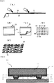
- Fig. 1 is a cross-sectional view showing a structure comprising an electronic component and a mounting body according to a first embodiment of the present invention.
- the structure will be described using a flexible thermistor 1A as one example of the electronic component.
- the aforementioned structure according to the present invention includes a flexible thermistor 1A having a metal substrate 11, a semiconductor ceramic layer 15 formed on the metal substrate 11, and a pair of split electrodes 21 and 22 formed on the semiconductor ceramic layer 15; and a printed circuit board 30 functioning as a mounting body on which lands 31 and 32 to be connected to the respective split electrodes 21 and 22 of the flexible thermistor 1A are formed.
- a Ni plating film 23 and an Sn plating film 24 are formed in this order on the surface of each of the split electrodes 21 and 22.
- a Ni plating film 23' and an Sn plating film 24' are formed on surfaces of the metal substrate 11.
- the reason for this is that when the Ni plating film 23 and the Sn plating film 24 are formed on the surface of each split electrode by electric field plating, the plating films are also inevitably formed on the metal substrate 11. In addition, when electric field plating is not used, the Ni plating film 23' and the Sn plating film 24' may not be always formed. In this case, although a protective layer 16 is formed on the surface of the semiconductor ceramic layer 15, this protective layer 16 may not be always formed.
- the positions of peripheral end portions of the lands 31 and 32 are located inside than the positions of peripheral end portions of the split electrodes 21 and 22, respectively.
- the positions of the peripheral end portions of the lands 31 and 32 to which solders 33 are to be applied are each farther than the position of a peripheral end portion of the metal substrate 11.
- the peripheral end portion of the metal substrate 11 indicates peripheral ends of side surfaces and end surfaces of the metal substrate 11.
- the peripheral end portion of each of the split electrodes 21 and 22 indicates a peripheral end portion which is located in a planar direction thereof and at a position adjacent to the peripheral end portion of the metal substrate 11.
- the peripheral end portion of each of the lands 31 and 32 indicates a peripheral end portion which is located in a planar direction parallel to the printed circuit board 30 and at a position adjacent to the peripheral end portion of the metal substrate 11.
- the positions of the peripheral end portions of the lands 31 and 32 are located inside than the positions of the peripheral end portions of the split electrodes 21 and 22, respectively, that is, are located inside than the peripheral end portion of the metal substrate 11.
- the distance between the metal substrate 11 and each of the lands 31 and 32 can be increased, and hence the solder 33 can be made to stay at the positions of the Ni plating film 23 and the Sn plating film 24, which are provided on each of the split electrodes 21 and 22. Hence, the solder 33 can be prevented from rising.
- the lands 31 and 32 provided on the printed circuit board 30 are frequently designed so as to have larger plane areas than those of the split electrodes 21 and 22, respectively, which are to be connected to the lands 31 and 32.
- the reason for this is to absorb displacement which occurs when the electronic component is mounted and to increase the degree of freedom in mounting.
- the solder 33 is liable to rise when the metal substrate 11 is located close to the mounting body or when the peripheral end portion of each of the lands 31 and 32 becomes closer to the peripheral end portion of the metal substrate 11 due to the formation of the Ni plating film 23' and the Sn plating film 24' on the surfaces of the metal substrate 11.
- Fig. 2(A) is a schematic plan view of a flexible thermistor 1B
- Fig. 2(B) is a front view thereof.
- the flexible thermistor 1B is a more simplified component of the flexible thermistor 1A.
- This flexible thermistor 1B includes a metal substrate 11, a semiconductor ceramic layer 15 formed on this metal substrate 11, and a pair of split electrodes 21 and 22 formed on this semiconductor ceramic layer 15.
- the metal substrate 11 is obtained by firing a sheet-shaped body formed from a metal powder paste
- the semiconductor ceramic layer 15 is obtained by firing a sheet-shaped body formed from a ceramic slurry
- the split electrodes 21 and 22 are each obtained by firing an electrode material paste.
- the sheet-shaped body formed from a metal powder paste, the sheet-shaped body formed from a ceramic slurry, and an electrode material paste are integrally fired.
- at least the metal substrate 11 and the semiconductor ceramic layer 15 may be obtained by integral firing.
- the thickness of the metal substrate 11 is approximately 10 to 80 ⁇ m
- the thickness of the semiconductor ceramic layer 15 is approximately 1 to 10 ⁇ m
- the thickness of each of the split electrodes 21 and 22 is approximately 0.1 to 10 ⁇ m
- the total thickness of the flexible thermistor 1B is approximately 10 to 100 ⁇ m.
- a ceramic material having an NTC characteristic and containing appropriate amounts of Mn, Ni, Fe, Ti, Co, Al, Zn, and the like in an arbitrary combination may be used.
- oxides of elements selected from the above transition metal elements are used and mixed together, a carbonate, a hydroxide, and/or the like of an element selected from the above elements may also be used as a starting raw material.
- a single noble metal such as Ag, Pd, Pt, or Au
- a single base metal such as Cu, Ni, Al, W, or Ti, or an alloy containing at least one of the above metals may be used.
- the metal substrate 11 and the semiconductor ceramic layer 15 may have a sheet shape.
- a doctor blade method is generally used, a screen printing method, a gravure printing method, or an ink jet method may also be used.
- the split electrodes 21 and 22 may be formed, for example, by a screen printing method, a sputtering method, or a deposition method.
- Fig. 3 is an equivalent circuit of the flexible thermistor 1B.
- the split electrodes 21 and 22 are used as an input and an output terminal, and resistances R1 and R2 are formed by the semiconductor ceramic layer 15 and are also electrically connected in series to each other through the metal substrate 11. That is, the resistances R1 and R2 formed by the semiconductor ceramic layer 15 provided in thickness direction between the metal substrate 11 and the split electrodes 21 and 22 form a thermistor circuit.
- Fig. 4 is a view showing a pathway of a current flowing through the flexible thermistor 1B described above. Since the split electrodes 21 and 22 are formed on the surface of the semiconductor ceramic layer 15, as shown by the arrows in Fig. 4 , the current passes along a pathway between two parts of the semiconductor ceramic layer 15, which are in contact with the split electrodes 21 and 22, via the metal substrate 11. Flexure of the flexible thermistor 1A is liable to occur, and when mounting is performed by a mounter, cracks are also liable to be generated in a central portion of the semiconductor ceramic layer 15. However, even if cracks are generated in the central portion of the semiconductor ceramic layer 15, the central portion is not the current pathway, and hence electrical characteristics as the flexible thermistor 1A are not adversely influenced.
- Fig. 5 includes views showing one example of a method for manufacturing the flexible thermistor 1A.
- oxides of Mn, Ni, Fe, Ti and/or the like are weighed to have a predetermined mixing ratio (in order to obtain a resistivity of 10 4 ⁇ cm) and are then sufficiently wet-pulverized using a ball mill with a pulverizing medium formed from zirconia and/or the like, and subsequently, calcination is performed at a predetermined temperature to obtain a ceramic powder.
- the slurry thus obtained is formed into a ceramic green sheet on a PET-made carrier film 31 by a doctor blade method so as to obtain a semiconductor ceramic layer 15 having a thickness of 1 to 15 ⁇ m after firing.
- a metal-substrate paste containing Ag-Pd as a primary component is formed into a metal substrate sheet on this ceramic green sheet by a doctor blade method so as to obtain a metal substrate 11 having a thickness of 5 to 100 ⁇ m after firing (see Fig. 5(B) ).
- the film 31, the sheet 15, and the sheet 11 are cut into a size of a mother sheet from which a plurality of components is to be formed, and the sheets 15 and 11 are then peeled away from the film 31 (see Fig. 5C ) .
- an Ag-Pd paste to be formed into the split electrodes 21 and 22 is applied by screen printing to form a laminate (see Fig. 5D ).
- the mother sheet in the form of a laminate is cut into thermistor units ( Fig. 5E ).
- one thermistor unit thus obtained is received in a zirconia-made container, or sagger and is then processed by a debinding treatment, firing is performed at a predetermined temperature (such as 900°C to 1, 300°C) .
- a predetermined temperature such as 900°C to 1, 300°C
- Example 1 a flexible thermistor formed by the following method was evaluated.
- an organic binder, a dispersant, and water were added to this calcined powder and were mixed together using zirconia balls for several hours to form a slurry, and the slurry thus obtained was processed by a doctor blade method into a ceramic green sheet so as to have a thickness of 5 ⁇ m after firing.
- a metal-substrate paste containing Ag-Pd as a primary component was applied on the ceramic green sheet thus obtained to form a metal substrate sheet to obtain a mother sheet so as to have a thickness of 30 ⁇ m after firing. Subsequently, an Ag-Pd paste was screen-printed on the ceramic green sheet to form unfired split electrodes.
- Ni plating film and an Sn plating film were formed by electrolytic plating on the thermistor obtained by firing.
- the Ni plating film and the Sn plating film were formed in this order on the surface of the metal substrate and the surfaces of the split electrodes.
- a split electrode side of the flexible thermistor thus obtained was arranged on Au-plated Cu-metal lands which were formed on a glass epoxy substrate, and using a lead-free solder containing Sn-Ag-Cu as a primary component, solder mounting was performed in a reflow furnace at a peak temperature of 260°C.
- the external dimensions of the obtained flexible thermistor were 1.0 mm ⁇ 0.5 mm ⁇ 0.040 mm.
- the dimensions of the formed split electrode, the dimensions of the land, a distance a from the peripheral end portion of the metal substrate to the peripheral end portion of the split electrode, a distance b from the peripheral end portion of the split electrode to the peripheral end portion of the land, and a distance c from the peripheral end portion of the metal substrate to the peripheral end portion of the land are shown in Table 1.
- a direct-current resistance of a solder-mounted flexible thermistor was measure by a direct-current four-terminal method in a liquid bath at a temperature of 25°C, and an incidence rate of short-circuit defects was evaluated.
- the number of evaluated thermistors was 1,000, and the incidence rate of short-circuit defects was calculated by (the number of short-circuited thermistors/1,000) ⁇ 100 (%).
- Fig. 6 is a cross-sectional view showing a mounting structure of an electronic component 2A according to a second aspect of the present disclosure.
- a protective layer 16' of an insulating material was formed on the entire surface of a metal substrate 11 except for parts thereof on which split electrodes 21 and 22 were formed. Accordingly, a Ni plating film 23 and an Sn plating film 24 formed on each of the split electrodes 21 and 22 could be reliably insulated from the metal substrate 11.
- solders 33 applied to lands 31 and 32 did not reach a peripheral side of the metal substrate 11 and could be reliably prevented from rising to the metal substrate 11.
Claims (6)
- Eine Struktur, die folgende Merkmale aufweist:eine Elektronikkomponente (1A), die ein Metallsubstrat (11), eine auf dem Metallsubstrat (11) gebildete Halbleiterkeramikschicht (15), ein Paar gespaltener Elektroden (21, 22), die auf der Halbleiterkeramikschicht (15) gebildet sind, und Plattierungsfilme (23, 24, 23', 24'), die auf den gespaltenen Elektroden (21, 22) und dem Metallsubstrat (11) gebildet sind, umfasst; undeinen Montagekörper (30), an dem Stege (31, 32) gebildet sind, die mit den jeweiligen gespaltenen Elektroden (21, 22) der Elektronikkomponente (1A) verbunden sind,dadurch gekennzeichnet, dasssie die Position eines peripheren Endabschnitts jedes Stegs (31, 32), der mit der entsprechenden gespaltenen Elektrode verbunden ist, weiter innen befindet als die Position eines peripheren Endabschnitts der gespaltenen Elektrode (21, 22),die Dicke des Metallsubstrats (11) der Elektronikkomponente (1A) 10 bis 80 µm beträgt und die Dicke der Keramikschicht (15) 1 bis 10 µm beträgt,sich die Position des peripheren Endabschnitts jeder gespaltenen Elektrode (21, 22) weiter innen befindet als eine Position eines peripheren Endabschnitts der Halbleiterkeramikschicht (15), undsich die Position des peripheren Endabschnitts jeder gespaltenen Elektrode (21, 22) weiter innen befindet als eine Position eines peripheren Endabschnitts des Metallsubstrats (11).
- Die Struktur gemäß Anspruch 1, bei der ein ebener Bereich jedes Stegs (31, 32) kleiner ist als der der entsprechenden gespaltenen Elektrode (21, 22).
- Die Struktur gemäß einem der Ansprüche 1 bis 2, bei der das Metallsubstrat (11) der Elektronikkomponente (1A) eine Lagenform aufweist, die aus einer Metallpulverpaste gebildet ist, und die Keramikschicht (15) eine Lagenform aufweist, die aus einer Keramikaufschlämmung gebildet ist.
- Die Struktur gemäß Anspruch 3, bei der das lagenförmige Metallsubstrat (11) und die lagenförmige Keramikschicht (15) durch Brennen erhalten werden, während sie integral miteinander laminiert werden.
- Die Struktur gemäß einem der Ansprüche 1 bis 4, die ferner eine Schutzschicht (16) aufweist, die aus einem Isoliermaterial auf zumindest einer Oberfläche der Keramikschicht (15) gebildet ist, auf der die gespaltenen Elektroden (21, 22) gebildet sind.
- Die Struktur gemäß einem der Ansprüche 1 bis 5, bei der ein Elektrolytische-Galvanisierung-Film (23', 24') auf einer Oberfläche des Metallsubstrats (11) gebildet ist.
Applications Claiming Priority (2)
| Application Number | Priority Date | Filing Date | Title |
|---|---|---|---|
| JP2011038764 | 2011-02-24 | ||
| PCT/JP2012/052655 WO2012114857A1 (ja) | 2011-02-24 | 2012-02-07 | 電子部品の実装構造 |
Publications (3)
| Publication Number | Publication Date |
|---|---|
| EP2680301A1 EP2680301A1 (de) | 2014-01-01 |
| EP2680301A4 EP2680301A4 (de) | 2016-05-25 |
| EP2680301B1 true EP2680301B1 (de) | 2020-05-06 |
Family
ID=46720643
Family Applications (1)
| Application Number | Title | Priority Date | Filing Date |
|---|---|---|---|
| EP12749782.4A Active EP2680301B1 (de) | 2011-02-24 | 2012-02-07 | Struktur umfassend elektronisches Bauteil und Montagekörper |
Country Status (5)
| Country | Link |
|---|---|
| US (1) | US9184362B2 (de) |
| EP (1) | EP2680301B1 (de) |
| JP (1) | JP5664760B2 (de) |
| CN (1) | CN103380492B (de) |
| WO (1) | WO2012114857A1 (de) |
Families Citing this family (6)
| Publication number | Priority date | Publication date | Assignee | Title |
|---|---|---|---|---|
| JP5668837B2 (ja) * | 2011-02-24 | 2015-02-12 | 株式会社村田製作所 | 電子部品の実装構造 |
| DE102011109007A1 (de) * | 2011-07-29 | 2013-01-31 | Epcos Ag | Verfahren zum Herstellen eines elektrischen Bauelements und elektrisches Bauelement |
| KR101670140B1 (ko) * | 2014-12-15 | 2016-10-27 | 삼성전기주식회사 | 저항 소자, 그 제조방법 및 저항 소자의 실장 기판 |
| JP6330924B2 (ja) * | 2015-02-06 | 2018-05-30 | 株式会社村田製作所 | パワー半導体モジュール |
| JP6668617B2 (ja) * | 2015-06-04 | 2020-03-18 | 富士電機株式会社 | サーミスタ搭載装置およびサーミスタ部品 |
| DE112018000095T5 (de) | 2017-02-21 | 2019-05-09 | Murata Manufacturing Co., Ltd. | Rfid-etikett |
Family Cites Families (16)
| Publication number | Priority date | Publication date | Assignee | Title |
|---|---|---|---|---|
| JPH0740509B2 (ja) * | 1984-07-24 | 1995-05-01 | 松下電器産業株式会社 | 発熱体 |
| JPS61193401A (ja) * | 1985-02-21 | 1986-08-27 | 株式会社村田製作所 | チツプ形正特性サ−ミスタ |
| JPS61242002A (ja) * | 1985-04-19 | 1986-10-28 | 松下電器産業株式会社 | 薄膜サ−ミスタ |
| JPS61245502A (ja) | 1985-04-23 | 1986-10-31 | 松下電器産業株式会社 | 薄膜サ−ミスタ |
| JPS6310502U (de) * | 1986-07-07 | 1988-01-23 | ||
| JPS63169793A (ja) | 1987-01-07 | 1988-07-13 | 株式会社村田製作所 | プリント基板へのチツプ部品の取付構造 |
| JPH01215034A (ja) * | 1988-02-24 | 1989-08-29 | Matsushita Electric Ind Co Ltd | 半導体装置 |
| JPH0438892A (ja) * | 1990-06-01 | 1992-02-10 | Mitsubishi Electric Corp | チップ部品の実装方法及び印刷配線板 |
| JPH06209158A (ja) * | 1993-01-12 | 1994-07-26 | Matsushita Electric Ind Co Ltd | 印刷配線板 |
| JPH06302406A (ja) * | 1993-04-19 | 1994-10-28 | Mitsubishi Materials Corp | チップ型サーミスタ及びその製造方法 |
| JPH1154301A (ja) * | 1997-08-07 | 1999-02-26 | Murata Mfg Co Ltd | チップ型サーミスタ |
| JP2003007510A (ja) * | 2002-06-19 | 2003-01-10 | Mitsubishi Materials Corp | チップ型サーミスタ |
| JP2005094243A (ja) * | 2003-09-16 | 2005-04-07 | Toyo Commun Equip Co Ltd | 多重モード圧電フィルタ素子、表面実装用フィルタ、圧電振動素子、及び表面実装用圧電振動子 |
| JP4265578B2 (ja) * | 2005-06-30 | 2009-05-20 | オムロン株式会社 | 回路基板 |
| US8198186B2 (en) * | 2008-12-31 | 2012-06-12 | Stats Chippac, Ltd. | Semiconductor device and method of confining conductive bump material during reflow with solder mask patch |
| CN102483978B (zh) * | 2009-08-28 | 2015-03-11 | 株式会社村田制作所 | 热敏电阻及其制造方法 |
-
2012
- 2012-02-07 WO PCT/JP2012/052655 patent/WO2012114857A1/ja active Application Filing
- 2012-02-07 EP EP12749782.4A patent/EP2680301B1/de active Active
- 2012-02-07 CN CN201280009531.6A patent/CN103380492B/zh not_active Expired - Fee Related
- 2012-02-07 JP JP2013500936A patent/JP5664760B2/ja not_active Expired - Fee Related
-
2013
- 2013-08-14 US US13/966,317 patent/US9184362B2/en not_active Expired - Fee Related
Non-Patent Citations (1)
| Title |
|---|
| None * |
Also Published As
| Publication number | Publication date |
|---|---|
| US9184362B2 (en) | 2015-11-10 |
| WO2012114857A1 (ja) | 2012-08-30 |
| EP2680301A1 (de) | 2014-01-01 |
| JPWO2012114857A1 (ja) | 2014-07-07 |
| JP5664760B2 (ja) | 2015-02-04 |
| CN103380492B (zh) | 2016-04-27 |
| EP2680301A4 (de) | 2016-05-25 |
| US20130328153A1 (en) | 2013-12-12 |
| CN103380492A (zh) | 2013-10-30 |
Similar Documents
| Publication | Publication Date | Title |
|---|---|---|
| EP2680301B1 (de) | Struktur umfassend elektronisches Bauteil und Montagekörper | |
| KR101099213B1 (ko) | 적층 세라믹 콘덴서 | |
| KR101107236B1 (ko) | 세라믹 전자부품 | |
| KR102139753B1 (ko) | 세라믹 전자 부품 및 이의 제조방법 | |
| EP2824681B1 (de) | Elektronisches bauteil und eine übergangsstruktur zwischen zu verbindendem elektronischen bauteil und objekt | |
| JP4636180B2 (ja) | 積層型セラミック電子部品 | |
| JP5668837B2 (ja) | 電子部品の実装構造 | |
| US7277003B2 (en) | Electrostatic discharge protection component | |
| US20060193103A1 (en) | Electronic component and electronic device | |
| KR101022980B1 (ko) | 세라믹 전자 부품 | |
| EP3196904B1 (de) | Keramische halbleiterelektronikkomponente in form eines chips | |
| US9667036B2 (en) | ESD protection component | |
| JP2004200373A (ja) | 電子部品および製造方法 | |
| JPH056805A (ja) | チツプ型バリスタ | |
| US11763993B2 (en) | Ceramic electronic device and mounting substrate | |
| JP2007013215A (ja) | 積層型チップバリスタ及びその製造方法、並びに積層型素子 | |
| JP4715000B2 (ja) | チップ型電子部品の製造方法 | |
| KR100709913B1 (ko) | 적층형 칩 배리스터, 이의 제조방법 및 적층형 소자 | |
| JP4295202B2 (ja) | チップ部品及びチップ部品の製造方法 | |
| KR101843252B1 (ko) | 칩 저항 소자 및 칩 저항 소자 어셈블리 | |
| JP4359267B2 (ja) | 導電体ペースト、積層型チップバリスタおよびその製造方法 | |
| KR20170095573A (ko) | 칩 저항 소자 및 칩 저항 소자 어셈블리 | |
| JP2013182930A (ja) | 積層型複合電子部品 | |
| JP2004273499A (ja) | 電極及び電子部品 |
Legal Events
| Date | Code | Title | Description |
|---|---|---|---|
| PUAI | Public reference made under article 153(3) epc to a published international application that has entered the european phase |
Free format text: ORIGINAL CODE: 0009012 |
|
| 17P | Request for examination filed |
Effective date: 20130807 |
|
| AK | Designated contracting states |
Kind code of ref document: A1 Designated state(s): AL AT BE BG CH CY CZ DE DK EE ES FI FR GB GR HR HU IE IS IT LI LT LU LV MC MK MT NL NO PL PT RO RS SE SI SK SM TR |
|
| DAX | Request for extension of the european patent (deleted) | ||
| RA4 | Supplementary search report drawn up and despatched (corrected) |
Effective date: 20160422 |
|
| RIC1 | Information provided on ipc code assigned before grant |
Ipc: H01L 21/60 20060101AFI20160418BHEP Ipc: H01C 1/14 20060101ALI20160418BHEP Ipc: H01C 7/04 20060101ALI20160418BHEP |
|
| GRAP | Despatch of communication of intention to grant a patent |
Free format text: ORIGINAL CODE: EPIDOSNIGR1 |
|
| STAA | Information on the status of an ep patent application or granted ep patent |
Free format text: STATUS: GRANT OF PATENT IS INTENDED |
|
| INTG | Intention to grant announced |
Effective date: 20191203 |
|
| GRAS | Grant fee paid |
Free format text: ORIGINAL CODE: EPIDOSNIGR3 |
|
| GRAA | (expected) grant |
Free format text: ORIGINAL CODE: 0009210 |
|
| STAA | Information on the status of an ep patent application or granted ep patent |
Free format text: STATUS: THE PATENT HAS BEEN GRANTED |
|
| AK | Designated contracting states |
Kind code of ref document: B1 Designated state(s): AL AT BE BG CH CY CZ DE DK EE ES FI FR GB GR HR HU IE IS IT LI LT LU LV MC MK MT NL NO PL PT RO RS SE SI SK SM TR |
|
| REG | Reference to a national code |
Ref country code: GB Ref legal event code: FG4D |
|
| REG | Reference to a national code |
Ref country code: AT Ref legal event code: REF Ref document number: 1268166 Country of ref document: AT Kind code of ref document: T Effective date: 20200515 Ref country code: CH Ref legal event code: EP |
|
| REG | Reference to a national code |
Ref country code: DE Ref legal event code: R096 Ref document number: 602012069910 Country of ref document: DE |
|
| REG | Reference to a national code |
Ref country code: IE Ref legal event code: FG4D |
|
| REG | Reference to a national code |
Ref country code: LT Ref legal event code: MG4D |
|
| REG | Reference to a national code |
Ref country code: NL Ref legal event code: MP Effective date: 20200506 |
|
| PG25 | Lapsed in a contracting state [announced via postgrant information from national office to epo] |
Ref country code: PT Free format text: LAPSE BECAUSE OF FAILURE TO SUBMIT A TRANSLATION OF THE DESCRIPTION OR TO PAY THE FEE WITHIN THE PRESCRIBED TIME-LIMIT Effective date: 20200907 Ref country code: LT Free format text: LAPSE BECAUSE OF FAILURE TO SUBMIT A TRANSLATION OF THE DESCRIPTION OR TO PAY THE FEE WITHIN THE PRESCRIBED TIME-LIMIT Effective date: 20200506 Ref country code: GR Free format text: LAPSE BECAUSE OF FAILURE TO SUBMIT A TRANSLATION OF THE DESCRIPTION OR TO PAY THE FEE WITHIN THE PRESCRIBED TIME-LIMIT Effective date: 20200807 Ref country code: FI Free format text: LAPSE BECAUSE OF FAILURE TO SUBMIT A TRANSLATION OF THE DESCRIPTION OR TO PAY THE FEE WITHIN THE PRESCRIBED TIME-LIMIT Effective date: 20200506 Ref country code: NO Free format text: LAPSE BECAUSE OF FAILURE TO SUBMIT A TRANSLATION OF THE DESCRIPTION OR TO PAY THE FEE WITHIN THE PRESCRIBED TIME-LIMIT Effective date: 20200806 Ref country code: SE Free format text: LAPSE BECAUSE OF FAILURE TO SUBMIT A TRANSLATION OF THE DESCRIPTION OR TO PAY THE FEE WITHIN THE PRESCRIBED TIME-LIMIT Effective date: 20200506 Ref country code: IS Free format text: LAPSE BECAUSE OF FAILURE TO SUBMIT A TRANSLATION OF THE DESCRIPTION OR TO PAY THE FEE WITHIN THE PRESCRIBED TIME-LIMIT Effective date: 20200906 |
|
| PG25 | Lapsed in a contracting state [announced via postgrant information from national office to epo] |
Ref country code: RS Free format text: LAPSE BECAUSE OF FAILURE TO SUBMIT A TRANSLATION OF THE DESCRIPTION OR TO PAY THE FEE WITHIN THE PRESCRIBED TIME-LIMIT Effective date: 20200506 Ref country code: BG Free format text: LAPSE BECAUSE OF FAILURE TO SUBMIT A TRANSLATION OF THE DESCRIPTION OR TO PAY THE FEE WITHIN THE PRESCRIBED TIME-LIMIT Effective date: 20200806 Ref country code: HR Free format text: LAPSE BECAUSE OF FAILURE TO SUBMIT A TRANSLATION OF THE DESCRIPTION OR TO PAY THE FEE WITHIN THE PRESCRIBED TIME-LIMIT Effective date: 20200506 Ref country code: LV Free format text: LAPSE BECAUSE OF FAILURE TO SUBMIT A TRANSLATION OF THE DESCRIPTION OR TO PAY THE FEE WITHIN THE PRESCRIBED TIME-LIMIT Effective date: 20200506 |
|
| REG | Reference to a national code |
Ref country code: AT Ref legal event code: MK05 Ref document number: 1268166 Country of ref document: AT Kind code of ref document: T Effective date: 20200506 |
|
| PG25 | Lapsed in a contracting state [announced via postgrant information from national office to epo] |
Ref country code: AL Free format text: LAPSE BECAUSE OF FAILURE TO SUBMIT A TRANSLATION OF THE DESCRIPTION OR TO PAY THE FEE WITHIN THE PRESCRIBED TIME-LIMIT Effective date: 20200506 Ref country code: NL Free format text: LAPSE BECAUSE OF FAILURE TO SUBMIT A TRANSLATION OF THE DESCRIPTION OR TO PAY THE FEE WITHIN THE PRESCRIBED TIME-LIMIT Effective date: 20200506 |
|
| PG25 | Lapsed in a contracting state [announced via postgrant information from national office to epo] |
Ref country code: RO Free format text: LAPSE BECAUSE OF FAILURE TO SUBMIT A TRANSLATION OF THE DESCRIPTION OR TO PAY THE FEE WITHIN THE PRESCRIBED TIME-LIMIT Effective date: 20200506 Ref country code: CZ Free format text: LAPSE BECAUSE OF FAILURE TO SUBMIT A TRANSLATION OF THE DESCRIPTION OR TO PAY THE FEE WITHIN THE PRESCRIBED TIME-LIMIT Effective date: 20200506 Ref country code: AT Free format text: LAPSE BECAUSE OF FAILURE TO SUBMIT A TRANSLATION OF THE DESCRIPTION OR TO PAY THE FEE WITHIN THE PRESCRIBED TIME-LIMIT Effective date: 20200506 Ref country code: ES Free format text: LAPSE BECAUSE OF FAILURE TO SUBMIT A TRANSLATION OF THE DESCRIPTION OR TO PAY THE FEE WITHIN THE PRESCRIBED TIME-LIMIT Effective date: 20200506 Ref country code: DK Free format text: LAPSE BECAUSE OF FAILURE TO SUBMIT A TRANSLATION OF THE DESCRIPTION OR TO PAY THE FEE WITHIN THE PRESCRIBED TIME-LIMIT Effective date: 20200506 Ref country code: IT Free format text: LAPSE BECAUSE OF FAILURE TO SUBMIT A TRANSLATION OF THE DESCRIPTION OR TO PAY THE FEE WITHIN THE PRESCRIBED TIME-LIMIT Effective date: 20200506 Ref country code: SM Free format text: LAPSE BECAUSE OF FAILURE TO SUBMIT A TRANSLATION OF THE DESCRIPTION OR TO PAY THE FEE WITHIN THE PRESCRIBED TIME-LIMIT Effective date: 20200506 Ref country code: EE Free format text: LAPSE BECAUSE OF FAILURE TO SUBMIT A TRANSLATION OF THE DESCRIPTION OR TO PAY THE FEE WITHIN THE PRESCRIBED TIME-LIMIT Effective date: 20200506 |
|
| REG | Reference to a national code |
Ref country code: DE Ref legal event code: R097 Ref document number: 602012069910 Country of ref document: DE |
|
| PG25 | Lapsed in a contracting state [announced via postgrant information from national office to epo] |
Ref country code: SK Free format text: LAPSE BECAUSE OF FAILURE TO SUBMIT A TRANSLATION OF THE DESCRIPTION OR TO PAY THE FEE WITHIN THE PRESCRIBED TIME-LIMIT Effective date: 20200506 Ref country code: PL Free format text: LAPSE BECAUSE OF FAILURE TO SUBMIT A TRANSLATION OF THE DESCRIPTION OR TO PAY THE FEE WITHIN THE PRESCRIBED TIME-LIMIT Effective date: 20200506 |
|
| PLBE | No opposition filed within time limit |
Free format text: ORIGINAL CODE: 0009261 |
|
| STAA | Information on the status of an ep patent application or granted ep patent |
Free format text: STATUS: NO OPPOSITION FILED WITHIN TIME LIMIT |
|
| 26N | No opposition filed |
Effective date: 20210209 |
|
| PG25 | Lapsed in a contracting state [announced via postgrant information from national office to epo] |
Ref country code: SI Free format text: LAPSE BECAUSE OF FAILURE TO SUBMIT A TRANSLATION OF THE DESCRIPTION OR TO PAY THE FEE WITHIN THE PRESCRIBED TIME-LIMIT Effective date: 20200506 |
|
| PG25 | Lapsed in a contracting state [announced via postgrant information from national office to epo] |
Ref country code: MC Free format text: LAPSE BECAUSE OF FAILURE TO SUBMIT A TRANSLATION OF THE DESCRIPTION OR TO PAY THE FEE WITHIN THE PRESCRIBED TIME-LIMIT Effective date: 20200506 |
|
| GBPC | Gb: european patent ceased through non-payment of renewal fee |
Effective date: 20210207 |
|
| REG | Reference to a national code |
Ref country code: BE Ref legal event code: MM Effective date: 20210228 |
|
| PG25 | Lapsed in a contracting state [announced via postgrant information from national office to epo] |
Ref country code: LU Free format text: LAPSE BECAUSE OF NON-PAYMENT OF DUE FEES Effective date: 20210207 Ref country code: LI Free format text: LAPSE BECAUSE OF NON-PAYMENT OF DUE FEES Effective date: 20210228 Ref country code: CH Free format text: LAPSE BECAUSE OF NON-PAYMENT OF DUE FEES Effective date: 20210228 |
|
| PG25 | Lapsed in a contracting state [announced via postgrant information from national office to epo] |
Ref country code: FR Free format text: LAPSE BECAUSE OF NON-PAYMENT OF DUE FEES Effective date: 20210228 Ref country code: GB Free format text: LAPSE BECAUSE OF NON-PAYMENT OF DUE FEES Effective date: 20210207 Ref country code: IE Free format text: LAPSE BECAUSE OF NON-PAYMENT OF DUE FEES Effective date: 20210207 |
|
| PG25 | Lapsed in a contracting state [announced via postgrant information from national office to epo] |
Ref country code: BE Free format text: LAPSE BECAUSE OF NON-PAYMENT OF DUE FEES Effective date: 20210228 |
|
| PG25 | Lapsed in a contracting state [announced via postgrant information from national office to epo] |
Ref country code: HU Free format text: LAPSE BECAUSE OF FAILURE TO SUBMIT A TRANSLATION OF THE DESCRIPTION OR TO PAY THE FEE WITHIN THE PRESCRIBED TIME-LIMIT; INVALID AB INITIO Effective date: 20120207 Ref country code: CY Free format text: LAPSE BECAUSE OF FAILURE TO SUBMIT A TRANSLATION OF THE DESCRIPTION OR TO PAY THE FEE WITHIN THE PRESCRIBED TIME-LIMIT Effective date: 20200506 |
|
| PGFP | Annual fee paid to national office [announced via postgrant information from national office to epo] |
Ref country code: DE Payment date: 20230216 Year of fee payment: 12 |