EP2673403B1 - Isoliertes metallsubstrat - Google Patents
Isoliertes metallsubstrat Download PDFInfo
- Publication number
- EP2673403B1 EP2673403B1 EP12706093.7A EP12706093A EP2673403B1 EP 2673403 B1 EP2673403 B1 EP 2673403B1 EP 12706093 A EP12706093 A EP 12706093A EP 2673403 B1 EP2673403 B1 EP 2673403B1
- Authority
- EP
- European Patent Office
- Prior art keywords
- coating
- ims
- substrate
- ims according
- nanoceramic
- Prior art date
- Legal status (The legal status is an assumption and is not a legal conclusion. Google has not performed a legal analysis and makes no representation as to the accuracy of the status listed.)
- Not-in-force
Links
Images


Classifications
-
- C—CHEMISTRY; METALLURGY
- C25—ELECTROLYTIC OR ELECTROPHORETIC PROCESSES; APPARATUS THEREFOR
- C25D—PROCESSES FOR THE ELECTROLYTIC OR ELECTROPHORETIC PRODUCTION OF COATINGS; ELECTROFORMING; APPARATUS THEREFOR
- C25D11/00—Electrolytic coating by surface reaction, i.e. forming conversion layers
- C25D11/02—Anodisation
- C25D11/024—Anodisation under pulsed or modulated current or potential
-
- H—ELECTRICITY
- H01—ELECTRIC ELEMENTS
- H01L—SEMICONDUCTOR DEVICES NOT COVERED BY CLASS H10
- H01L23/00—Details of semiconductor or other solid state devices
- H01L23/12—Mountings, e.g. non-detachable insulating substrates
- H01L23/14—Mountings, e.g. non-detachable insulating substrates characterised by the material or its electrical properties
- H01L23/142—Metallic substrates having insulating layers
-
- C—CHEMISTRY; METALLURGY
- C25—ELECTROLYTIC OR ELECTROPHORETIC PROCESSES; APPARATUS THEREFOR
- C25D—PROCESSES FOR THE ELECTROLYTIC OR ELECTROPHORETIC PRODUCTION OF COATINGS; ELECTROFORMING; APPARATUS THEREFOR
- C25D11/00—Electrolytic coating by surface reaction, i.e. forming conversion layers
-
- C—CHEMISTRY; METALLURGY
- C25—ELECTROLYTIC OR ELECTROPHORETIC PROCESSES; APPARATUS THEREFOR
- C25D—PROCESSES FOR THE ELECTROLYTIC OR ELECTROPHORETIC PRODUCTION OF COATINGS; ELECTROFORMING; APPARATUS THEREFOR
- C25D11/00—Electrolytic coating by surface reaction, i.e. forming conversion layers
- C25D11/005—Apparatus specially adapted for electrolytic conversion coating
-
- C—CHEMISTRY; METALLURGY
- C25—ELECTROLYTIC OR ELECTROPHORETIC PROCESSES; APPARATUS THEREFOR
- C25D—PROCESSES FOR THE ELECTROLYTIC OR ELECTROPHORETIC PRODUCTION OF COATINGS; ELECTROFORMING; APPARATUS THEREFOR
- C25D11/00—Electrolytic coating by surface reaction, i.e. forming conversion layers
- C25D11/02—Anodisation
- C25D11/026—Anodisation with spark discharge
-
- C—CHEMISTRY; METALLURGY
- C25—ELECTROLYTIC OR ELECTROPHORETIC PROCESSES; APPARATUS THEREFOR
- C25D—PROCESSES FOR THE ELECTROLYTIC OR ELECTROPHORETIC PRODUCTION OF COATINGS; ELECTROFORMING; APPARATUS THEREFOR
- C25D11/00—Electrolytic coating by surface reaction, i.e. forming conversion layers
- C25D11/02—Anodisation
- C25D11/04—Anodisation of aluminium or alloys based thereon
- C25D11/06—Anodisation of aluminium or alloys based thereon characterised by the electrolytes used
-
- C—CHEMISTRY; METALLURGY
- C25—ELECTROLYTIC OR ELECTROPHORETIC PROCESSES; APPARATUS THEREFOR
- C25D—PROCESSES FOR THE ELECTROLYTIC OR ELECTROPHORETIC PRODUCTION OF COATINGS; ELECTROFORMING; APPARATUS THEREFOR
- C25D11/00—Electrolytic coating by surface reaction, i.e. forming conversion layers
- C25D11/02—Anodisation
- C25D11/26—Anodisation of refractory metals or alloys based thereon
-
- C—CHEMISTRY; METALLURGY
- C25—ELECTROLYTIC OR ELECTROPHORETIC PROCESSES; APPARATUS THEREFOR
- C25D—PROCESSES FOR THE ELECTROLYTIC OR ELECTROPHORETIC PRODUCTION OF COATINGS; ELECTROFORMING; APPARATUS THEREFOR
- C25D11/00—Electrolytic coating by surface reaction, i.e. forming conversion layers
- C25D11/02—Anodisation
- C25D11/30—Anodisation of magnesium or alloys based thereon
-
- C—CHEMISTRY; METALLURGY
- C25—ELECTROLYTIC OR ELECTROPHORETIC PROCESSES; APPARATUS THEREFOR
- C25D—PROCESSES FOR THE ELECTROLYTIC OR ELECTROPHORETIC PRODUCTION OF COATINGS; ELECTROFORMING; APPARATUS THEREFOR
- C25D11/00—Electrolytic coating by surface reaction, i.e. forming conversion layers
- C25D11/02—Anodisation
- C25D11/32—Anodisation of semiconducting materials
-
- C—CHEMISTRY; METALLURGY
- C25—ELECTROLYTIC OR ELECTROPHORETIC PROCESSES; APPARATUS THEREFOR
- C25D—PROCESSES FOR THE ELECTROLYTIC OR ELECTROPHORETIC PRODUCTION OF COATINGS; ELECTROFORMING; APPARATUS THEREFOR
- C25D11/00—Electrolytic coating by surface reaction, i.e. forming conversion layers
- C25D11/02—Anodisation
- C25D11/34—Anodisation of metals or alloys not provided for in groups C25D11/04 - C25D11/32
-
- C—CHEMISTRY; METALLURGY
- C25—ELECTROLYTIC OR ELECTROPHORETIC PROCESSES; APPARATUS THEREFOR
- C25D—PROCESSES FOR THE ELECTROLYTIC OR ELECTROPHORETIC PRODUCTION OF COATINGS; ELECTROFORMING; APPARATUS THEREFOR
- C25D13/00—Electrophoretic coating characterised by the process
- C25D13/02—Electrophoretic coating characterised by the process with inorganic material
-
- C—CHEMISTRY; METALLURGY
- C25—ELECTROLYTIC OR ELECTROPHORETIC PROCESSES; APPARATUS THEREFOR
- C25D—PROCESSES FOR THE ELECTROLYTIC OR ELECTROPHORETIC PRODUCTION OF COATINGS; ELECTROFORMING; APPARATUS THEREFOR
- C25D13/00—Electrophoretic coating characterised by the process
- C25D13/18—Electrophoretic coating characterised by the process using modulated, pulsed, or reversing current
-
- C—CHEMISTRY; METALLURGY
- C25—ELECTROLYTIC OR ELECTROPHORETIC PROCESSES; APPARATUS THEREFOR
- C25D—PROCESSES FOR THE ELECTROLYTIC OR ELECTROPHORETIC PRODUCTION OF COATINGS; ELECTROFORMING; APPARATUS THEREFOR
- C25D15/00—Electrolytic or electrophoretic production of coatings containing embedded materials, e.g. particles, whiskers, wires
-
- C—CHEMISTRY; METALLURGY
- C25—ELECTROLYTIC OR ELECTROPHORETIC PROCESSES; APPARATUS THEREFOR
- C25D—PROCESSES FOR THE ELECTROLYTIC OR ELECTROPHORETIC PRODUCTION OF COATINGS; ELECTROFORMING; APPARATUS THEREFOR
- C25D21/00—Processes for servicing or operating cells for electrolytic coating
- C25D21/12—Process control or regulation
-
- C—CHEMISTRY; METALLURGY
- C25—ELECTROLYTIC OR ELECTROPHORETIC PROCESSES; APPARATUS THEREFOR
- C25D—PROCESSES FOR THE ELECTROLYTIC OR ELECTROPHORETIC PRODUCTION OF COATINGS; ELECTROFORMING; APPARATUS THEREFOR
- C25D5/00—Electroplating characterised by the process; Pretreatment or after-treatment of workpieces
- C25D5/18—Electroplating using modulated, pulsed or reversing current
-
- C—CHEMISTRY; METALLURGY
- C25—ELECTROLYTIC OR ELECTROPHORETIC PROCESSES; APPARATUS THEREFOR
- C25D—PROCESSES FOR THE ELECTROLYTIC OR ELECTROPHORETIC PRODUCTION OF COATINGS; ELECTROFORMING; APPARATUS THEREFOR
- C25D5/00—Electroplating characterised by the process; Pretreatment or after-treatment of workpieces
- C25D5/60—Electroplating characterised by the structure or texture of the layers
- C25D5/605—Surface topography of the layers, e.g. rough, dendritic or nodular layers
- C25D5/611—Smooth layers
-
- C—CHEMISTRY; METALLURGY
- C25—ELECTROLYTIC OR ELECTROPHORETIC PROCESSES; APPARATUS THEREFOR
- C25D—PROCESSES FOR THE ELECTROLYTIC OR ELECTROPHORETIC PRODUCTION OF COATINGS; ELECTROFORMING; APPARATUS THEREFOR
- C25D5/00—Electroplating characterised by the process; Pretreatment or after-treatment of workpieces
- C25D5/60—Electroplating characterised by the structure or texture of the layers
- C25D5/615—Microstructure of the layers, e.g. mixed structure
- C25D5/617—Crystalline layers
-
- C—CHEMISTRY; METALLURGY
- C25—ELECTROLYTIC OR ELECTROPHORETIC PROCESSES; APPARATUS THEREFOR
- C25D—PROCESSES FOR THE ELECTROLYTIC OR ELECTROPHORETIC PRODUCTION OF COATINGS; ELECTROFORMING; APPARATUS THEREFOR
- C25D5/00—Electroplating characterised by the process; Pretreatment or after-treatment of workpieces
- C25D5/60—Electroplating characterised by the structure or texture of the layers
- C25D5/623—Porosity of the layers
-
- H—ELECTRICITY
- H01—ELECTRIC ELEMENTS
- H01L—SEMICONDUCTOR DEVICES NOT COVERED BY CLASS H10
- H01L23/00—Details of semiconductor or other solid state devices
- H01L23/34—Arrangements for cooling, heating, ventilating or temperature compensation ; Temperature sensing arrangements
- H01L23/36—Selection of materials, or shaping, to facilitate cooling or heating, e.g. heatsinks
- H01L23/373—Cooling facilitated by selection of materials for the device or materials for thermal expansion adaptation, e.g. carbon
- H01L23/3735—Laminates or multilayers, e.g. direct bond copper ceramic substrates
-
- H—ELECTRICITY
- H05—ELECTRIC TECHNIQUES NOT OTHERWISE PROVIDED FOR
- H05K—PRINTED CIRCUITS; CASINGS OR CONSTRUCTIONAL DETAILS OF ELECTRIC APPARATUS; MANUFACTURE OF ASSEMBLAGES OF ELECTRICAL COMPONENTS
- H05K1/00—Printed circuits
- H05K1/02—Details
- H05K1/0201—Thermal arrangements, e.g. for cooling, heating or preventing overheating
- H05K1/0203—Cooling of mounted components
- H05K1/021—Components thermally connected to metal substrates or heat-sinks by insert mounting
-
- H—ELECTRICITY
- H05—ELECTRIC TECHNIQUES NOT OTHERWISE PROVIDED FOR
- H05K—PRINTED CIRCUITS; CASINGS OR CONSTRUCTIONAL DETAILS OF ELECTRIC APPARATUS; MANUFACTURE OF ASSEMBLAGES OF ELECTRICAL COMPONENTS
- H05K1/00—Printed circuits
- H05K1/02—Details
- H05K1/03—Use of materials for the substrate
- H05K1/05—Insulated conductive substrates, e.g. insulated metal substrate
- H05K1/053—Insulated conductive substrates, e.g. insulated metal substrate the metal substrate being covered by an inorganic insulating layer
-
- H—ELECTRICITY
- H05—ELECTRIC TECHNIQUES NOT OTHERWISE PROVIDED FOR
- H05K—PRINTED CIRCUITS; CASINGS OR CONSTRUCTIONAL DETAILS OF ELECTRIC APPARATUS; MANUFACTURE OF ASSEMBLAGES OF ELECTRICAL COMPONENTS
- H05K1/00—Printed circuits
- H05K1/02—Details
- H05K1/11—Printed elements for providing electric connections to or between printed circuits
- H05K1/115—Via connections; Lands around holes or via connections
-
- H—ELECTRICITY
- H05—ELECTRIC TECHNIQUES NOT OTHERWISE PROVIDED FOR
- H05K—PRINTED CIRCUITS; CASINGS OR CONSTRUCTIONAL DETAILS OF ELECTRIC APPARATUS; MANUFACTURE OF ASSEMBLAGES OF ELECTRICAL COMPONENTS
- H05K1/00—Printed circuits
- H05K1/18—Printed circuits structurally associated with non-printed electric components
-
- H—ELECTRICITY
- H01—ELECTRIC ELEMENTS
- H01L—SEMICONDUCTOR DEVICES NOT COVERED BY CLASS H10
- H01L2224/00—Indexing scheme for arrangements for connecting or disconnecting semiconductor or solid-state bodies and methods related thereto as covered by H01L24/00
- H01L2224/01—Means for bonding being attached to, or being formed on, the surface to be connected, e.g. chip-to-package, die-attach, "first-level" interconnects; Manufacturing methods related thereto
- H01L2224/42—Wire connectors; Manufacturing methods related thereto
- H01L2224/47—Structure, shape, material or disposition of the wire connectors after the connecting process
- H01L2224/48—Structure, shape, material or disposition of the wire connectors after the connecting process of an individual wire connector
- H01L2224/481—Disposition
- H01L2224/48151—Connecting between a semiconductor or solid-state body and an item not being a semiconductor or solid-state body, e.g. chip-to-substrate, chip-to-passive
- H01L2224/48221—Connecting between a semiconductor or solid-state body and an item not being a semiconductor or solid-state body, e.g. chip-to-substrate, chip-to-passive the body and the item being stacked
- H01L2224/48225—Connecting between a semiconductor or solid-state body and an item not being a semiconductor or solid-state body, e.g. chip-to-substrate, chip-to-passive the body and the item being stacked the item being non-metallic, e.g. insulating substrate with or without metallisation
- H01L2224/48227—Connecting between a semiconductor or solid-state body and an item not being a semiconductor or solid-state body, e.g. chip-to-substrate, chip-to-passive the body and the item being stacked the item being non-metallic, e.g. insulating substrate with or without metallisation connecting the wire to a bond pad of the item
-
- H—ELECTRICITY
- H01—ELECTRIC ELEMENTS
- H01L—SEMICONDUCTOR DEVICES NOT COVERED BY CLASS H10
- H01L2224/00—Indexing scheme for arrangements for connecting or disconnecting semiconductor or solid-state bodies and methods related thereto as covered by H01L24/00
- H01L2224/01—Means for bonding being attached to, or being formed on, the surface to be connected, e.g. chip-to-package, die-attach, "first-level" interconnects; Manufacturing methods related thereto
- H01L2224/42—Wire connectors; Manufacturing methods related thereto
- H01L2224/47—Structure, shape, material or disposition of the wire connectors after the connecting process
- H01L2224/49—Structure, shape, material or disposition of the wire connectors after the connecting process of a plurality of wire connectors
- H01L2224/491—Disposition
- H01L2224/49105—Connecting at different heights
- H01L2224/49109—Connecting at different heights outside the semiconductor or solid-state body
-
- H—ELECTRICITY
- H01—ELECTRIC ELEMENTS
- H01L—SEMICONDUCTOR DEVICES NOT COVERED BY CLASS H10
- H01L23/00—Details of semiconductor or other solid state devices
- H01L23/34—Arrangements for cooling, heating, ventilating or temperature compensation ; Temperature sensing arrangements
- H01L23/36—Selection of materials, or shaping, to facilitate cooling or heating, e.g. heatsinks
- H01L23/367—Cooling facilitated by shape of device
- H01L23/3677—Wire-like or pin-like cooling fins or heat sinks
-
- H—ELECTRICITY
- H01—ELECTRIC ELEMENTS
- H01L—SEMICONDUCTOR DEVICES NOT COVERED BY CLASS H10
- H01L2924/00—Indexing scheme for arrangements or methods for connecting or disconnecting semiconductor or solid-state bodies as covered by H01L24/00
- H01L2924/013—Alloys
- H01L2924/0132—Binary Alloys
- H01L2924/01327—Intermediate phases, i.e. intermetallics compounds
-
- H—ELECTRICITY
- H01—ELECTRIC ELEMENTS
- H01L—SEMICONDUCTOR DEVICES NOT COVERED BY CLASS H10
- H01L2924/00—Indexing scheme for arrangements or methods for connecting or disconnecting semiconductor or solid-state bodies as covered by H01L24/00
- H01L2924/095—Indexing scheme for arrangements or methods for connecting or disconnecting semiconductor or solid-state bodies as covered by H01L24/00 with a principal constituent of the material being a combination of two or more materials provided in the groups H01L2924/013 - H01L2924/0715
- H01L2924/097—Glass-ceramics, e.g. devitrified glass
- H01L2924/09701—Low temperature co-fired ceramic [LTCC]
-
- H—ELECTRICITY
- H01—ELECTRIC ELEMENTS
- H01L—SEMICONDUCTOR DEVICES NOT COVERED BY CLASS H10
- H01L2924/00—Indexing scheme for arrangements or methods for connecting or disconnecting semiconductor or solid-state bodies as covered by H01L24/00
- H01L2924/10—Details of semiconductor or other solid state devices to be connected
- H01L2924/11—Device type
- H01L2924/13—Discrete devices, e.g. 3 terminal devices
- H01L2924/1304—Transistor
- H01L2924/1305—Bipolar Junction Transistor [BJT]
- H01L2924/13055—Insulated gate bipolar transistor [IGBT]
-
- H—ELECTRICITY
- H05—ELECTRIC TECHNIQUES NOT OTHERWISE PROVIDED FOR
- H05K—PRINTED CIRCUITS; CASINGS OR CONSTRUCTIONAL DETAILS OF ELECTRIC APPARATUS; MANUFACTURE OF ASSEMBLAGES OF ELECTRICAL COMPONENTS
- H05K2201/00—Indexing scheme relating to printed circuits covered by H05K1/00
- H05K2201/01—Dielectrics
- H05K2201/0104—Properties and characteristics in general
- H05K2201/0116—Porous, e.g. foam
-
- H—ELECTRICITY
- H05—ELECTRIC TECHNIQUES NOT OTHERWISE PROVIDED FOR
- H05K—PRINTED CIRCUITS; CASINGS OR CONSTRUCTIONAL DETAILS OF ELECTRIC APPARATUS; MANUFACTURE OF ASSEMBLAGES OF ELECTRICAL COMPONENTS
- H05K2203/00—Indexing scheme relating to apparatus or processes for manufacturing printed circuits covered by H05K3/00
- H05K2203/03—Metal processing
- H05K2203/0315—Oxidising metal
-
- H—ELECTRICITY
- H05—ELECTRIC TECHNIQUES NOT OTHERWISE PROVIDED FOR
- H05K—PRINTED CIRCUITS; CASINGS OR CONSTRUCTIONAL DETAILS OF ELECTRIC APPARATUS; MANUFACTURE OF ASSEMBLAGES OF ELECTRICAL COMPONENTS
- H05K2203/00—Indexing scheme relating to apparatus or processes for manufacturing printed circuits covered by H05K3/00
- H05K2203/11—Treatments characterised by their effect, e.g. heating, cooling, roughening
- H05K2203/1147—Sealing or impregnating, e.g. of pores
-
- Y—GENERAL TAGGING OF NEW TECHNOLOGICAL DEVELOPMENTS; GENERAL TAGGING OF CROSS-SECTIONAL TECHNOLOGIES SPANNING OVER SEVERAL SECTIONS OF THE IPC; TECHNICAL SUBJECTS COVERED BY FORMER USPC CROSS-REFERENCE ART COLLECTIONS [XRACs] AND DIGESTS
- Y10—TECHNICAL SUBJECTS COVERED BY FORMER USPC
- Y10T—TECHNICAL SUBJECTS COVERED BY FORMER US CLASSIFICATION
- Y10T428/00—Stock material or miscellaneous articles
- Y10T428/13—Hollow or container type article [e.g., tube, vase, etc.]
- Y10T428/131—Glass, ceramic, or sintered, fused, fired, or calcined metal oxide or metal carbide containing [e.g., porcelain, brick, cement, etc.]
- Y10T428/1317—Multilayer [continuous layer]
-
- Y—GENERAL TAGGING OF NEW TECHNOLOGICAL DEVELOPMENTS; GENERAL TAGGING OF CROSS-SECTIONAL TECHNOLOGIES SPANNING OVER SEVERAL SECTIONS OF THE IPC; TECHNICAL SUBJECTS COVERED BY FORMER USPC CROSS-REFERENCE ART COLLECTIONS [XRACs] AND DIGESTS
- Y10—TECHNICAL SUBJECTS COVERED BY FORMER USPC
- Y10T—TECHNICAL SUBJECTS COVERED BY FORMER US CLASSIFICATION
- Y10T428/00—Stock material or miscellaneous articles
- Y10T428/24—Structurally defined web or sheet [e.g., overall dimension, etc.]
- Y10T428/24802—Discontinuous or differential coating, impregnation or bond [e.g., artwork, printing, retouched photograph, etc.]
- Y10T428/24917—Discontinuous or differential coating, impregnation or bond [e.g., artwork, printing, retouched photograph, etc.] including metal layer
-
- Y—GENERAL TAGGING OF NEW TECHNOLOGICAL DEVELOPMENTS; GENERAL TAGGING OF CROSS-SECTIONAL TECHNOLOGIES SPANNING OVER SEVERAL SECTIONS OF THE IPC; TECHNICAL SUBJECTS COVERED BY FORMER USPC CROSS-REFERENCE ART COLLECTIONS [XRACs] AND DIGESTS
- Y10—TECHNICAL SUBJECTS COVERED BY FORMER USPC
- Y10T—TECHNICAL SUBJECTS COVERED BY FORMER US CLASSIFICATION
- Y10T428/00—Stock material or miscellaneous articles
- Y10T428/249921—Web or sheet containing structurally defined element or component
- Y10T428/249953—Composite having voids in a component [e.g., porous, cellular, etc.]
- Y10T428/249967—Inorganic matrix in void-containing component
- Y10T428/249969—Of silicon-containing material [e.g., glass, etc.]
Definitions
- the invention relates to insulated metal substrates, for example insulated metal substrates as used to support electronic, optoelectronic, microwave, RF and electrical devices.
- a substrate on which such a device can be mounted is known as an insulated metal substrate (IMS).
- IMS insulated metal substrate
- IMSs Insulated metal substrates
- IMSs are typically used for electronic devices that generate high specific heat energy, for example in high power electronics, solid-state lighting, telecommunication and concentrated photovoltaic applications.
- IMSs usually comprise a metal sheet base covered from one side or two sides by an insulating layer of dielectric material, which may be polymeric, for example resin, fluoropolymer, polyimide and their composites charged with thermally conductive ceramic powders, etc.
- dielectric material which may be polymeric, for example resin, fluoropolymer, polyimide and their composites charged with thermally conductive ceramic powders, etc.
- Such sheet IMS often named as Metal Core Printed Circuit Boards (MC PCB) then are usually attached to a heat think through a layer of thermal interface material.
- MC PCB Metal Core Printed Circuit Boards
- a dielectric layer can be formed directly on a heat sink by use of anodising as described in GB 2162694 , or Plasma Electrolytic Oxidation (PEO) as described in US Pat. 6919012B1 or US Pat. 2008257585A1 .
- PEO Plasma Electrolytic Oxidation
- An IMS which may be a metal board, a heat sink, a device body or supporting frame, requires dielectric material to have a high dielectric strength to secure electric insulation from circuitry of the device, thereby avoiding or preventing the device from short-circuiting. Thermal conductivity of dielectric material is also required to dissipate heat generated by the device, which negatively effects performance, reliability and the lifetime of the device. In general, an increased dielectric strength enables the IMS to have a thinner insulating layer, which is reducing IMS thermal resistance (with the same thermal conductivity of insulating material).
- an IMS comprises a dielectric material that has a high dielectric constant.
- the problem is solved by the insulated metal substrate for supporting a device as defined in claim 1.
- Advantageous additional aspects follow from the dependent claims. Subject-matter described herein which does not fall under the wording of the claims is provided as an illustrative example and does not form part of the invention.
- Ceramic coatings produced PEO techniques have pores of significantly greater size than 500 nanometres.
- the nanoscale of the porosity on the IMS according to this aspect of the invention may contribute to various beneficial mechanical and electrical properties.
- a low average pore diameter may improve the dielectric strength of a coating.
- a high dielectric strength may mean that the coating thickness required to achieve a predetermined minimum dielectric strength for any particular application is lowered, which in turn may improve the thermal conductivity of the coating.
- a lower pore size may also improve the thermal conductivity of the coating by improving the heat flow path through the coating.
- the pores of the coating have an average size of less than 400 nanometres, particularly preferably less than 300 nanometres.
- metallic and semi-metallic as used herein are intended to describe broad classes of material. Thus, these terms describe elemental metals such as pure aluminium or magnesium and elemental semi-metals such as silicon, as well as alloys of one or more elements, and intermetallic compounds. Practically, the substrates used in the methods of the invention are likely to be commercially available metallic or semi-metallic compositions.
- An IMS may be preferably formed from a substrate made from aluminium, magnesium, titanium, zirconium, tantalum, beryllium, or an alloy or intermetallic of any of these metals.
- the dielectric strength of a coating is of particular importance.
- the coating of an IMS according to any aspect of the present invention may, advantageously, provide a dielectric strength of between 50 and 120 kV mm -1 .
- the coating provides a dielectric strength in the range of 60 to 100 kV mm -1 .
- the thermal conductivity of a coating is high.
- An insulating coating is required to provide electrical insulation between a working electronic component or device and a substrate, and simultaneously conduct heat away from this component into the substrate. It may be advantageous, therefore, that the coating of an IMS according to any aspect of the invention has a thermal conductivity of greater than 5 W/mK. Preferably, the thermal conductivity is between 5 and 14 W/mK.
- the dielectric coating has a high dielectric constant.
- a high dielectric constant may be particularly preferred when the IMS is intended to be used in RF or microwave applications.
- the IMS comprises a dielectric coating with a dielectric constant greater than 7.
- the dielectric constant is greater than 7.5 or greater than 8.
- the dielectric coating is between 7 and 12, for example between 7.5 and 10.
- the coating of an IMS according to any aspect of the present invention is a crystalline ceramic coating, and preferably the coating comprises grains having an average diameter of less than 200 nanometres, particularly preferably less than 100 nanometres, for example about 50 nanometres or 40 nanometres. Grains may be alternatively referred to as crystals or crystallites.
- a preferred embodiment of an IMS may comprise a coating that may be described as a nanostructured coating, or a nanoceramic coating, as it has physical features that have a size or dimensions on the nanometre scale. Fine grain sizes may improve structural homogeneity and properties such as hardness, wear resistance. Fine grain sizes may also increase thermal conductivity, dielectric strength and dielectric constant of a ceramic material. A smoother surface profile may also be developed as a result of the fine grain size.
- a coating formed on a metal substrate by an anodising process tends to be highly porous.
- Anodised coatings also usually have an amorphous structure (i.e. anodised coatings are rarely crystalline) and an open, column-like structure.
- the regular column-like structure of a typical anodic coating may render the coating susceptible to the formation of cracks, particularly after thermal cycling of the coating.
- the susceptibility to crack formation limits the application of anodic coatings in power devices.
- an IMS in which the dielectric layer has been formed by an anodic coating process is generally limited to low power applications in which the thermal cycling of the coating may be minimised.
- an IMS having a dielectric coating formed by an anodising process may be suitable for many low power applications, such coatings do not have a sufficient voltage withstand or thermal conductivity for high power applications.
- Coatings produced by PEO processes are crystalline, but suffer in that the average porosity size is high. This limits the dielectric properties and thermal conductivity.
- Some advanced IMSs are produced using dielectric coatings based on ceramic filled polymers having a high thermal conductivity of up to 3 W/mK. This high thermal conductivity is due to the presence of relatively large ceramic particles in the material. The minimal thickness obtainable by the use of insulating layers of this material is limited, however, due to the presence of the ceramic particles.
- a coating of an IMS material produced by BergquistTM has a minimal thickness of 38 microns.
- DupontTM produces an IMS with a polyimide based dielectric material having a minimal thickness of 17 microns.
- IMSs according to any aspect of the present invention may be formed with a dielectric coating that is thinner than 17 micrometres, where such coating thickness is desirable.
- Table 1 A comparison of dielectric layer properties between the coating of the present invention and other known dielectrics.
- An IMS according to any aspect of the present invention is an IMS for supporting an electronic device, an optoelectronic device, a microwave or RF device or an electrical device.
- the thickness of the non-metallic coating is preferably less than 40 micrometres, and particularly preferably less than 20 micrometres or less than 10 micrometres. The thinner the coating the more effective the thermal transfer across the coating, and thus it may be particularly advantageous if the coatings have thicknesses even lower, for example in the range 1 or 2 micrometres to 10 micrometres.
- An IMS according to an embodiment of the invention may preferably have a coating thickness of less than 11 microns, the coating having a breakdown voltage greater than 500 V DC, and a thermal resistance of less 0.02°C cm 2 /W.
- An IMS according to an embodiment of the invention may have a coating with thickness less than 31 micrometres, a breakdown voltage of greater than 1.5 KV DC and thermal resistance lower 0.07°C cm 2 /W.
- An IMS according to any aspect of the invention may comprise a dielectric coating that has been applied selectively to a portion of a metal or semi-metal substrate or component.
- the substrate or component may be of any desired shape, and may form a component such as a flat board, a heat-sink, a heat pipe, a cooling device, or a luminary frame or body.
- the substrate or component on which the coating is to be formed may be, for example, masked such that the coating is only applied to a predetermined region where dielectric functionality is desired.
- an IMS according to any aspect of the invention may comprise a dielectric coating that has been sealed or impregnated by a suitable organic or inorganic material to fill any pores in the coating.
- a suitable sealing material may be, for example, a resin, a fluoropolymer, a polyimide, a methacrylate, a polyester, a water glass, or a sol-gel material. This list of suitable sealing materials is not exhaustive and the skilled person would be able to identify other suitable materials. Sealing materials may be applied to the coating by a number of known methods, for example by dipping, spraying, vacuum sealing, and PVD and CVD deposition techniques.
- An IMS according to any aspect of the invention further comprises one or more metal contact layers or areas formed on a surface of the coating.
- Such contact layers or areas may be provided by any conventional techniques such as screen printing, metal ink printing, electroless metallisation, galvanic metallisation, adhesive bonding of metal foil, bonding of pre-fabricated flex circuits, chemical vapour deposition (CVD) and plasma vapour deposition (PVD) metallisation.
- CVD chemical vapour deposition
- PVD plasma vapour deposition
- Metal contact layers may be formed by the use of thermally conductive adhesives to bond metallic foils, such as copper foils, or pre-fabricated flex circuits to the coating formed as described above.
- Suitable thermally conductive adhesives may include resins, polyimides or fluoropolymers and others for bonding a metal layer to the surface of the coating. Bonding using adhesives may be accompanied by penetration of the bonding material into any pores of the coating. This penetration may create a composite dielectric layer having an increased breakdown voltage.
- An IMS according to any aspect of the invention may comprise metal thermal vias connecting a metal contact layer formed on a surface of the non-metallic coating with the metallic or semi metallic substrate.
- Such vias may be formed by a masking process prior to the formation of the coating.
- Vias may be formed by an etching process after the coating has been formed or by laser ablation of ceramic layer.
- the substrate is selected from a group of materials comprising aluminium, magnesium, titanium, zirconium, tantalum, beryllium, or an alloy or intermetallic of any of these metals.
- a preferred embodiment of an IMS according to an aspect of the invention that is particularly suitable for RF or microwave applications may comprise a metallic substrate having a ceramic coating formed at least in part by electrolytic oxidation of a portion of the surface of the metallic substrate, in which the ceramic coating has a dielectric strength of greater than 50 KV mm -1 , a thermal conductivity of greater than 5 W m -1 K -1 , a thickness of between 500 nanometres and 500 micrometres , a crystalline structure having an average grain size of less than 500 nanometres, and a dielectric constant greater than 7, and in which pores defined in a surface of the ceramic coating have an average diameter of less than 500 nanometres
- a non-metallic coating possessing the desired properties is formed on a metallic or semi-metallic substrate.
- Metallic contact layers, tracks and pads may then be formed on the non-metallic coating if, or as, required.
- a preferred method of forming an IMS comprises the steps of positioning a metallic or semi-metallic substrate in an electrolysis chamber containing an aqueous electrolyte and an electrode. At least the surface of the substrate on which it is desired to form a crystalline ceramic coating and a portion of the electrode are in contact with the aqueous electrolyte.
- the substrate may be, for example, shaped as a heat sink, and may comprise a flat surface on which it is desired to form the coating.
- the method comprises the further step of electrically biasing the substrate with respect to the electrode by applying a sequence of voltage pulses of alternating polarity for a predetermined period.
- Positive voltage pulses anodically bias the substrate with respect to the electrode and negative voltage pulses cathodically bias the substrate with respect to the electrode.
- the amplitude of the positive voltage pulses is potentiostatically controlled, that is controlled with respect to voltage, and the amplitude of the negative voltage pulses is galvanostatically controlled, that is controlled by reference to current.
- the IMS of the present invention is formed at least in part by electrolytic oxidation of a portion of the surface of the metallic substrate, the electrolytic oxidation occurring under conditions in which micro-discharge is avoided. This may be achieved if the positive and negative voltage pulses are shaped to avoid the development of current spikes during each voltage pulse. Current spikes are associated with the breakdown of the coating and with micro-discharge. By shaping the voltage pulses to avoid current spikes, micro-discharge may be reduced significantly or eliminated. Micro-discharge, as discussed above in relation to prior art PEO coating techniques, has a deleterious effect on a number of coating properties, for example on the average pore size of the coating and, as a consequence, on the dielectric strength of the coating.
- the shape of one or both of the positive and negative voltage pulses is substantially trapezoidal in shape.
- the conversion of material in the substrate to form a ceramic coating occurs during the positive voltage pulses in which the substrate is anodically biased with respect to the electrode.
- the coating is formed as oxygen containing species in the aqueous electrolyte react with the substrate material itself.
- the non-metallic coating increases in thickness.
- the electrical resistance of the coating increases and less current flows for the applied voltage.
- the peak voltage of each of the positive voltage pulses is constant over the predetermined period, the current flow with each successive voltage pulse may decrease over the predetermined period.
- a dense coating may be formed having crystallites or grain size of extremely fine scale.
- the grain size of the coating formed is less than 200 nanometres, particularly preferably less than 100 nanometres, for example less than 50 nanometres.
- grain size refers to the distance across the average dimension of a grain or crystal in the coating.
- the pulse repetition frequency of the voltage pulses may be between 0.1 and 20 KHz, preferably between 1.5 and 15 KHz, or between 2 and 10 KHz.
- advantageous pulse repetition frequencies may be 2.5 KHz or 3 KHz or 4 KHz.
- the coating undergoes long period of growth followed by long periods of ohmic heating.
- the resulting coating may, therefore, have a more coarse structure or surface profile than if a higher pulse repetition frequency were to be used.
- Higher pulse repetition frequencies may produce finer structures and smoother coating surfaces, but coating rates and efficiency of the process may decrease.
- an electrolyte that is an alkaline aqueous solution, preferably an electrolyte having a pH of 9 or greater.
- the electrolyte has an electrical conductivity of greater than 1 mS cm -1 .
- Suitable electrolytes include alkaline metal hydroxides, particularly those comprising potassium hydroxide or sodium hydroxide.
- the electrolyte is colloidal and comprises solid particles dispersed in an aqueous phase.
- the electrolyte comprises a proportion of solid particles having a particle size of less than 100 nanometres.
- Particle size refers to the length of the largest dimension of the particle.
- an electric field generated during the applied voltage pulses causes electrostatically charged solid particles dispersed in the aqueous phase to be transported towards the surface of the substrate on which the non-metallic coating is growing. As the solid particles come into contact with the growing ceramic coating they may react with, and become incorporated into, the coating.
- the coating may comprise both ceramic material formed by oxidation of a portion of the surface of the metallic substrate and colloidal particles derived from the electrolyte.
- the coating forming on the substrate is generated during the positive, anodic, voltage pulses.
- a connection needs to be maintained between the substrate material and the electrolyte.
- the growing coating is not fully dense, but has a degree of porosity.
- the connection between the substrate material and the electrolyte is maintained via this porosity.
- the electrolyte is colloidal and comprises solid particles the porosity that is inherent in the formation of the ceramic coating may be substantially modified.
- Non-metallic solid particles dispersed in the aqueous phase may migrate under the electric field into pores of the growing coating. Once within the pores the solid particles may react, for example by sintering processes, with both the coating and with other solid particles that have migrated into the pores.
- the dimensions of the pores are substantially reduced and the porosity of the coating is altered develops as nanoporosity.
- the maximum dimensions of pores in the coating may be reduced from 1 or more micrometers across to less than 400 nanometres across or less than 300 nanometres across.
- the density of the coating is increased. Furthermore, the reduction in the dimensions of the porosity through the coating may substantially increase the dielectric strength and thermal conductivity of the coating.
- the electrolyte may comprise solid particles that are present from the start of the process, i.e. the particles may be initially present in the electrolyte solution.
- solid particles may be added to the aqueous electrolyte during the coating process. In this way, the composition and/or structure of the growing coating may be controlled while the coating is growing.
- the solid particles are ceramic particles, for example crystalline ceramic particles or glass particles, and that a proportion of the particles have maximum dimensions lower than 100 nanometres. It is particularly preferred that the solid particles are one or more metallic oxides or hydroxides of an element selected from the group comprising silicon, aluminium, titanium, iron, magnesium, tantalum, and the rare earth metals.
- a further preferred method of forming an IMS comprises the steps of positioning the substrate in an electrolytic chamber containing a colloidal electrolyte comprising solid particles dispersed in an aqueous phase.
- the chamber also contains an electrode. At least the surface of the substrate and a portion of the electrode are arranged to be contacting the electrolyte.
- the method comprises the step of electrically biasing the substrate relative to the electrode for a predetermined period of time to generate a ceramic dielectric coating on the surface of the substrate.
- a series of bipolar electric pulses are applied, such that the polarity of the substrate cycles from being anodic with respect to the electrode to being cathodic with respect to the electrode.
- the ceramic coating is formed during periods of the cycle during which the substrate is anodic with respect to the electrode.
- Solid particles from the colloidal electrolyte have a characteristic isoelectric point, and the pH corresponding to this isoelectric point differs from the pH of the aqueous phase of the electrolyte by 1.5 or greater.
- the solid particles migrate towards the surface of the substrate under the influence of an applied electric field and are incorporated into the non-metallic layer to form the non-metallic coating.
- the predetermined time during which the process is carried out may be any time required to provide a suitable thickness of coating for an intended purpose.
- the predetermined time may be between 1 minute and 2 hours.
- the rate of development of the coating may depend on a number of factors including the waveform used to bias the substrate relative to the electrode, and the density and size of particles in the colloidal electrolyte, where the method employs a colloidal electrolyte. It is particularly preferable that the predetermined time is between 2 minutes and 30 minutes, for example between 3 minutes and 15 minutes.
- An apparatus suitable for forming a dielectric coating on the surface of a metallic or semi-metallic substrate to form an IMS may comprise an electrolysis chamber for containing an aqueous electrolyte, an electrode locatable within the electrolysis chamber, and a power supply capable of applying a sequence of voltage pulses of alternative polarity between the substrate and the electrode.
- the power supply comprises a first pulse generator for generating a potentiostatically controlled sequence positive voltage pulses for anodically biasing the substrate with respect to the electrode.
- the power supply further comprises a second pulse generator for generating a galvanostatically controlled sequence of negative voltage pulses to cathodically bias the substrate with respect to the electrode.
- the apparatus further comprises a colloidal electrolyte comprising solid particles dispersed in an aqueous phase.
- a colloidal electrolyte comprising solid particles dispersed in an aqueous phase.
- the solid particles dispersed in such an electrolyte may become incorporated into the coating generated using the apparatus.
- the colloidal electrolyte may be any electrolyte as disclosed above in relation to the methods according to the invention.
- one aspect of the invention may further provide an IMS comprising a coating formed by any method described above or using the apparatus described above.
- the invention may provide a device incorporating or mounted onto an IMS according to any aspect above.
- An IMS according to the invention has superior dielectric and thermal conductivity properties compared to prior art IMSs, and devices mounted upon one may operate more efficiently due to the improved thermal transfer from components of the device through the IMS.
- Such thermal transfer may be achieved by a combination of improved dielectric strength of the coating on the IMS, which allows the coating to be thinner while providing electrical insulation, and an improved thermal conductivity of the material.
- An ability to apply an insulating layer directly onto the surface of a heat sink, heat pipe, cooling device, luminary frame or body enables devices to be formed having a minimal thermal path between working semiconductor elements and metal heat sinking elements. Examples of such devices include chip-on- heat sink, chip-on-heat pipe, chip-on- cooler, and chip -on- frame devices.
- an IMS having a multilayered structure may prove advantageous.
- an IMS may be formed according to any aspect or embodiment described above, and this IMS may then form the base of a multilayered IMS.
- An additional layer or layers of dielectric material and associated metal conducting layers may then be formed on the top of metal layer of the base IMS.
- the additional dielectric layer or layers may be, for example, FR-4 fibreglass laminates, or a fluoropolymer or polyimide layer.
- Electronic devices may advantageously be attached to the non-metallic coating of the base IMS (i.e. the non-metallic coating formed according to the electrolytic process described above), which provides high thermal conductivity.
- the multilayered structure formed on the base IMS may enable a large number of external connections to be made.
- FIG. 1 is a schematic illustration showing the structure of a specific embodiment of an IMS.
- the IMS 10 comprises a metal substrate 11, for example an aluminium substrate, that has a ceramic dielectric coating 12 formed on a surface of the substrate by any method described above.
- the ceramic coating is a crystalline coating having an average crystal size of less than 500 nanometres and may, therefore, be referred to as a nanoceramic coating.
- a metal contact layer 13 is formed on the surface of the nanoceramic coating 12.
- the metal substrate may have different shapes and may have different functions.
- the metal substrate may be a flat board for MC PCB use, the surface of a heat sink, the surface of a liquid cooled device, the surface of a heat pipe, or the surface of luminary frame.
- the skilled person may be aware of many further applications.
- Table 1 above provides a comparison of dielectric properties between a non-metallic coating of an IMS according to the present invention and prior art dielectric coatings currently used for IMS applications.
- nanoceramic coatings formed as the dielectric of an IMS according to an embodiment of the present invention have higher thermal conductivity than prior art IMS dielectrics. Moreover the relatively high minimal thickness of the prior art IMS dielectrics is excessive for low voltage applications, e.g. for LEDs. It will require only a 10 microns thickness of a nanoceramic coating as described herein to meet the requirements for 500 V DC breakdown voltage devices. The thermal resistance value of a 10 microns thick nanoceramic coating layer is less than 0.02 °C cm 2 /W, which is significantly lower than the thermal resistance of the other dielectric layers in table 1.
- a combination of higher thermal conductivity, dielectric strength and ability to tune the thickness of the coating within a broad range of 2-100 microns to meet necessary breakdown voltage requirement, provides that ability to create IMSs with unique thermal properties.
- an IMS may be formed by generating a nanoceramic coating on a suitable metal or non-metal.
- an IMS may be formed by generating a nanoceramic coating and then further coating the nanoceramic coating with a contact metal layer or layers using known techniques.
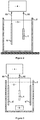
- FIG. 2 illustrates a typical apparatus suitable for forming a nanoceramic coating on a metallic or semi-metallic substrate 1 to form an IMS embodying the invention.
- the apparatus comprises a chemically inert tank 2, for example a tank formed from a stainless steel alloy, which contains an electrolyte solution 3.
- the electrolyte solution 3 is an aqueous alkaline electrolyte solution, for example an aqueous solution of sodium hydroxide or potassium hydroxide, and has an electrical conductivity of greater than 5 mS cm -1 .
- the electrolyte may be a colloidal electrolyte comprising solid particles, with a proportion of those particles having a particle size lower than 100 nanometres.
- the substrate 1 is electrically connected to a first output 50 of a pulse power supply 4.
- An electrode 5 is connected to a second output 55 of the pulse power supply 4, and both the electrode 5 and the substrate 1 are immersed in the electrolyte solution 3 contained within the tank 2.
- the pulse power supply 4 is capable of supplying electrical pulses of alternating polarity in order to electrically bias the substrate 1 with respect to the electrode 5.
- Figure 3 illustrates an alternative electrolytic apparatus suitable for fabricating an IMS according to one or more aspects or embodiments of the invention.
- the apparatus of Figure 3 comprises a chemically inert tank 2 for containing an electrolyte solution 3.
- a substrate 1 is coupled to a first output 50 of a pulse power supply 4.
- a second output 55 of the power supply 4 is electrically connected to first and second electrodes 5' and 5", and the substrate 1 and the electrodes 5' and 5" are immersed in the electrolyte 3.
- the two electrodes 5', 5" are disposed on either side of the substrate 1 in order to generate a more even electric field over the surface of the substrate and produce a more even coating on both sides of the substrate.
- more than two electrodes may be coupled to an output of the pulse power supply 4 should this be desired.
- more than one substrate may be simultaneously coupled to an output of the pulse power supply 4 so that more than one IMS may be formed at any one time.
- the apparatus of Figure 3 further comprises a heat exchanger 6 through which the electrolyte 3 is circulated.
- the heat exchanger 6 allows circulation of electrolyte 3 within the tank 2, and furthermore allows control of the temperature of the electrolyte.
- a preferred pulse power supply for use with an apparatus or method of forming an IMS embodying the invention, is capable of supplying separate positive and negative voltage pulses between the substrate and an electrode.
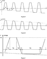
- a schematic diagram of a preferred pulse generator is illustrated in Figure 4 .
- the pulse power supply of Figure 4 comprises two separate insulated gate bipolar transistor (IGBT) based generators and is a preferred pulse power supply for the apparatus of Figures 2 or 3 .
- a first generator, or anodic generator, 30 acts a generator of anodic pulses, i.e. pulses that anodically bias the substrate, or substrates, with respect to the electrode, or electrodes.
- a second generator, or cathodic generator, 35 acts as a generator of cathodic pulses, i.e. pulses that cathodically bias the substrate, or substrates, with respect to the electrode, or electrodes.
- the anodic pulse generator 30 and the cathodic pulse generator 35 are independently controlled and synchronised by means of a controller 40.
- the anodic pulse generator 30 generates trapezoidal-shaped pulses having a fixed voltage amplitude, i.e. the voltage amplitude of the pulses generated by the anodic pulse generator 30 is potentiostatically controlled.
- the cathodic pulse generator 35 provides trapezoidal-shaped pulses in which the mean cathodic current is maintained at a fixed value over successive pulses, i.e. the cathodic pulse generator 35 generates pulses that are galvanostatically controlled.
- An output switch 45 comprising an H-bridge electronic circuit, couples the anodic pulse generator 30 and the cathodic pulse generator 35 to a first output 50 and a second output 55.
- the first output 50 is electrically coupled to a substrate and the second output 55 is electrically coupled to one or more electrodes.
- the controller 40 synchronises the output of the anodic pulse generator 30 and the cathodic pulse generator 35 and allows the output switch 45 to produce an output waveform comprising a sequence of positive and negative trapezoidal-shaped voltage pulses as illustrated in Figure 5 .
- FIG. 5 A particularly preferred waveform for use in a method of producing an IMS according to one or more aspects or embodiments of the invention is illustrated by Figures 5, 6 and 7 .
- Figure 5 illustrates a waveform consisting of a sequence of alternating positive and negative voltage pulses generated over a period of time.
- Positive voltage pulses are substantially trapezoidal in shape and have a positive pulse interval (T a ) as indicated in Figure 5 .
- T a positive pulse interval
- positive voltage pulses When applied between a substrate and an electrode, positive voltage pulses cause the substrate to be anodically biased relative to the electrode.
- Successive positive voltage pulses are controlled to have substantially the same voltage amplitude (V a ).
- Negative voltage pulses are substantially trapezoidal in shape and have a negative pulse interval T c .
- negative voltage pulses When applied between a substrate and an electrode, negative voltage pulses cause the substrate to be cathodically biased relative to the electrode. Successive negative voltage pulses are controlled to have substantially the same current amplitude (I c in Figure 6 ).
- the amplitude of each successive negative voltage pulse is controlled to be a voltage at which a constant level of current flows across the electrolyte.
- the application of the waveform results in a non-metallic coating being formed on the surface of the substrate. As the coating grows thicker, its electrical resistance increases and the voltage required to pass the same amount of current increases. Thus, the amplitude of successive cathodic voltage pulses (V c ) increases over a period of time.
- Figure 6 is a diagram showing the current waveform that corresponds to the voltage waveform illustrated in Figure 5 .
- a positive voltage pulse When a positive voltage pulse is applied a positive current is deemed to flow, and when a negative voltage is applied a negative current is deemed to flow.
- the positive voltage pulses are potentiostatically controlled, such that the amplitude of each successive pulse is substantially the same. Over a period of time the thickness of the coating on the surface of the substrate increases, and the current driven by this voltage decreases. Thus, the positive current pulse amplitude (I a ) associated with the positive voltage pulses tend to decrease over the period of time.
- negative voltage pulses are controlled galvanostatically, and thus these pulses are controlled to have a constant current amplitude (I c ).
- FIG 7 illustrates a portion of the waveform of Figure 5 showing one positive voltage pulse and one negative voltage pulse.
- Each positive voltage pulse is substantially trapezoidal in shape and has an interval (T ai ) during which the voltage rises from zero to the positive or anodic voltage amplitude (V a ).
- Each positive voltage pulse has an interval (T ac ) during which constant voltage is applied. This constant voltage is applied at the voltage amplitude of the pulse (V a ).
- Each positive voltage pulse further comprises an interval (T ad ) during which the voltage decreases from the voltage amplitude (V a ) to zero.
- the intervals (T ai ) and (T ad ) may be varied to control the current flow associated with the voltage pulse. It is highly undesirable that current spikes are generated during voltage pulses as current spikes promote the breakdown of the growing coating and cause micro-discharge or plasma generation. Micro-discharge events have a deleterious effect on the quality of the dielectric coating formed on the substrate.
- Each negative voltage pulse is substantially trapezoidal in shape and comprises three intervals analogous to the three intervals described in relation to the positive voltage pulses.
- Each cathodic voltage pulse has an interval (T ci ) during which voltage is increased from zero to the cathodic voltage amplitude (V c ) of that pulse, an interval during which the cathodic voltage remains at the cathodic voltage amplitude (V c ) and an interval (T cd ) during which the voltage decreases from the voltage amplitude (V c ) to zero.
- the voltage amplitude (V c ) is determined with respect to the current flow at the voltage. Thus, the voltage amplitude (V c ) tends to increase over a period of time, as illustrated in Figure 5 .
- the waveforms illustrated in Figures 5, 6 and 7 have a number of variables that may be controlled to influence the physical and electrical properties of the coating formed.
- the duration of both the positive and negative voltage pulses (T a & T c ) may be independently controlled.
- the intervals (T ai , T ac , T ad , T ci , T cc and T cd ) associated with the positive and negative voltage pulses can be controlled in order to substantially eliminate current pulse sparks and micro-discharge.
- the amplitude of the positive voltage pulses (V a ) may be controlled, as may the current flow at the peak voltage of each of the negative voltage pulses (I c ).
- the frequency of the pulses may be varied within a range of 100 Hz to 20 KHz.
- Figures 2 to 7 and the accompanying text describe apparatus and a preferred waveform suitable for generating a nanoceramic coating on the surface of a metallic or semi-metallic substrate in order to form an IMS.
- IMSs Specific embodiments of IMSs according to one or more aspects of the invention are described in the following examples. These examples were formed using apparatus as illustrated in Figures 2 or 3 , including the pulse generator illustrated in Figure 4 , and using the specific waveforms as illustrated in Figures 5 to 7 .
- the colloidal solutions comprise some solid particles with a particle size lower than 100 nanometres.
- Example 1 illustrates the formation of a nanoceramic coating on a metallic substrate that would be suitable for use as the dielectric of an IMS embodying the invention.
- a substrate in the form of a plate of Al 6082 alloy having dimensions of 50mmx50mm x1mm was treated in an apparatus as described above and illustrated in Figure 2 .
- the apparatus comprised a tank containing an electrolyte, and the substrate and an electrode were coupled to a pulse power supply as described above and illustrated in Figure 4 .
- the substrate and the electrode were arranged in contact with the electrolyte.
- the electrolyte was an aqueous solution containing 1.8 g/l of KOH and 1.0 g/l of Alumina particles, forming a stabilised colloidal solution.
- the Pulse Generator applied a sequence of trapezoidally-shaped voltage pulses of alternating polarity between the substrate and the electrode. Positive voltage pulses were applied having a fixed positive voltage amplitude (V a ) of 700 V, and negative voltage pulses had a negative voltage amplitude (V c ) continuously grown from 0 to 350 V.
- the pulse repetition frequency was 2.5 KHz.
- the pulses were applied for 8 minutes and a nanoceramic coating was formed on the surface of the substrate.
- the nanoceramic coating was characterised and had the following characteristics:
- the nanoceramic coating had a smooth surface profile.
- Figure 8 illustrates an SEM micrograph showing a portion of the coating at a magnification of 60,000 times. It can be seen that the surface is substantially smooth at this magnification.
- Figure 9 is a further SEM micrograph showing a portion of the coating at a magnification of 55,000 times. Pores in the coating having a size of between 50 an 150 nanometres can be seen. Pores of this dimension may be termed nano-pores.
- Figures 10 and 11 show SEM micrographs of a coating formed on the surface of an aluminium alloy by means of a plasma electrochemical oxidation (PEO) process. These micrographs are at a magnification of 50,000 times. The surface of the PEO coating can be seen to be extremely rough at this magnification. Pores formed by plasma bulbs can be seen to have a size of greater than 500 nanometres, in great contrast to the coating illustrated in Figure 8 and 9 .
- PEO plasma electrochemical oxidation
- the coating thickness was 20 micrometers and its hardness was measured to be 1550 Hv.
- An XRD analysis of the coating ( Figure 12 , revealed that the composition of the coating was aluminium oxide and that the coating having mean crystalline grain size of 40 nm. The average crystalline size was calculated on the base of the XRD data according to the Scherrer equation ( B.D. Cullity & S.R. Stock, Elements of X-Ray Diffraction, 3rd Ed., Prentice-Hall Inc., 2001, p 167-171 ).
- the breakdown voltage of the coating was measured to be 1800 V DC and the dielectric strength was measured to be 90 KV/mm.
- Thermal conductivity of the ceramic material was measured to be 6 W/mK.
- Dielectric constant of the ceramic material was measured to be 9.5.
- Figure 13 illustrates the use of an IMS embodying the invention as a metal heat sink for a high power device 64 such as for example a high-brightness light-emitting-diode (HB LED) chip. This may be described as a chip on heat sink application.
- a high power device 64 such as for example a high-brightness light-emitting-diode (HB LED) chip. This may be described as a chip on heat sink application.
- HB LED high-brightness light-emitting-diode
- a nanoceramic dielectric coating 62 is applied on a flat surface of a metal heat sink 61 to form an IMS.
- the nanoceramic coating is formed using the method described above in example 1.
- Metal contact tracks with pads 63 are then formed on the surface of the nanoceramic coating 62.
- the device 64 is attached directly to the nanoceramic coating 62, which provides electrical insulation between the chip and the metal heat sink 61.
- Contact connectors 65 are attached to connect the device 64 with the contact pads 63.
- the thickness of the nanoceramic coating is determined by the breakdown voltage requirement of the device, and is grown to the minimum thickness that meets the breakdown voltage requirement. This provides the shortest thermal path between non-insulated semiconductor components in the chip, which generate heat, and the metal heat sink 61.
- Figure 14 illustrates the use of an IMS embodying the invention as a metal heat sink for a packaged device 64, or a chip requiring a low resistance ground path.
- a nanoceramic dielectric coating 62 is applied on a flat surface of a metal heat sink 61 using the method described above in example 1, the metal heat sink 61 acting as a metal substrate for the nanoceramic coating 62.
- Metal contact tracks with pads 63 and a metal pad 66 are then formed on the surface of the nanoceramic coating 62.
- Thermal vias 67 defined through the nanoceramic coating 62 have metallic cores that connect the metal pad 66 and the metal heat sink 61.
- the device 64 is attached to the metal pad 66 and contact connectors 65 are attached to contact pads 63.
- Figure 15 illustrates the use of an IMS embodying the invention as part of a multilayered IMS board for a chip requiring a large number of external connections.
- An aluminium plate 61 acts as a metal substrate and performs a heat sinking function.
- a dielectric nanoceramic coating 62 is formed on one side of the aluminium plate 61, using the method described in example 1 above, and metal tracks 63 are formed on the surface of the nanoceramic coating 62.
- a chip 64 is attached directly to the surface of the nanoceramic dielectric coating 62, which provides low thermal resistance between the chip 64 and the aluminium substrate 61. Electrical signals necessary to control the chip are fed through the metal tracks 69 and 63, providing a high degree of integration of the system.
- Contact connectors 65 are attached to connect the device with various contact pads (metal tracks 69 and 63).
- Figure 16 illustrates a multilayered board for a radio chip with high thermal emission and high-frequency input / output signals.
- An aluminium carrier plate 61 acts as a metal substrate for the formation of a nanoceramic dielectric coating 62, and also performs both a heat sink function as well as a function of a radio frequency (RF) ground plane.
- RF radio frequency
- a dielectric nanoceramic coating 62 is formed selectively on one side of the aluminium carrier plate 61 to form an IMS (using the method described in example 1 above), and this IMS is used as a high Q dielectric media to carry RF signals.
- Metal tracks 63 are formed on the surface of the nanoceramic coating 62 and are used as a RF transmission lines.
- Further metal tracks 71 are formed on the surface of the dielectric coating 62 and act as RF de-coupling and/or matching circuits 71.
- Further dielectric layers 68 formed from FR4 fibreglass are located on the top of the metal tracks 63, with further metal tracks 69 formed on the surface of each of the fibreglass dielectric layers 68. This forms a fibreglass laminate structure. Metal tracks 69 may be interconnected by signal vias 70 defined through one or more of the fibreglass dielectric layers 68.
- Low frequency and/or digital signals necessary to control the chip are fed through metal tracks 69 in the fibreglass laminate, providing a high degree of integration of the system.
- the chip 64 is attached directly to the surface of the base metal plate 61.
- RF circuits 71 are formed on the surface of the dielectric nanoceramic layer 62.
- the dielectric nanoceramic coating 62 provides high-Q input / output transmission lines, used for RF de-coupling and/or matching circuits and low thermal resistance.
- Wirebonds 65 couple the chip 64 with contact tracks 69 and pads of the RF circuits 71.
Claims (15)
- Isoliertes Metallsubstrat (IMS) (10) zum Tragen einer Vorrichtung, wobei das IMS ein metallisches Substrat (11) mit einer nanokeramischen Beschichtung (12, 62) und einer auf einer Oberfläche der nanokeramischen Beschichtung gebildeten Metallkontaktschicht (13) aufweist, bei dem die nanokeramische Beschichtung wenigstens teilweise durch elektrolytische Oxidation eines Teils der Oberfläche des metallischen Substrats gebildet wird, wobei die elektrolytische Oxidation unter Bedingungen stattfindet, bei denen eine Mikroentladung vermieden wird, bei dem die Beschichtung eine Dicke zwischen 500 Nanometer und 500 Mikrometer und ein Kristallgefüge mit einer durchschnittlichen Korngröße von weniger als 500 Nanometer hat und bei dem in einer Oberfläche der Beschichtung definierte Poren einen Durchschnittsdurchmesser von weniger als 500 Nanometer haben, wobei die Beschichtung eine Durchschlagfestigkeit von mehr als 50 kV mm-1 und eine Wärmeleitfähigkeit von mehr als 5 W/mK hat.
- IMS nach Anspruch 1, bei dem in einer Oberfläche der nanokeramischen Beschichtung definierte Poren einen Durchschnittsdurchmesser von weniger als 400 Nanometer, vorzugsweise weniger als 300 Nanometer oder weniger als 200 Nanometer haben und/oder bei dem die nanokeramische Beschichtung eine Durchschlagfestigkeit zwischen 50 und 120 kV mm-1 und eine Wärmeleitfähigkeit zwischen 5 und 14 W/mK hat.
- IMS nach einem der vorhergehenden Ansprüche, bei dem die nanokeramische Beschichtung eine relative Dielektrizitätskonstante von mehr als 7 hat und/oder bei dem die nanokeramische Beschichtung Körner oder Kristallite mit einer Durchschnittsgröße von weniger als 250 Nanometer, vorzugsweise weniger als 100 Nanometer hat.
- IMS nach einem der vorhergehenden Ansprüche zum Tragen von einer oder mehr Vorrichtungen, die aus der Liste bestehend aus einer elektronischen Vorrichtung, einer optoelektronischen Vorrichtung, einer HF-Vorrichtung, einer Mikrowellenvorrichtung oder einer elektrischen Vorrichtung ausgewählt ist bzw. sind, und/oder IMS nach einem der vorhergehenden Ansprüche, bei dem die Dicke der nanokeramischen Beschichtung weniger als 50 Mikrometer, vorzugsweise weniger als 20 Mikrometer oder weniger als 10 Mikrometer ist.
- IMS nach einem der vorhergehenden Ansprüche, das wenigstens eine elektronische Schaltung trägt.
- IMS nach einem der vorhergehenden Ansprüche, bei dem die nanokeramische Beschichtung eine Dicke von weniger als 11 Mikrometer, eine Durchschlagspannung von mehr als 500 V DC und einen Wärmewiderstand von weniger als 0,02°C cm2/W hat oder bei dem die nanokeramische Beschichtung eine Dicke von weniger als 31 Mikrometer, eine Durchschlagspannung von mehr als 1,5 kV DC und einen Wärmewiderstand von weniger als 0,07 °C cm2/W hat.
- IMS nach einem der vorhergehenden Ansprüche, bei dem die Metallkontaktschicht durch einen aus der Liste bestehend aus Siebdruck, Metalltintendruck, stromlose Metallisierung, galvanische Metallisierung, Aufkleben von Metallfolie, Bonden vorgefertigter Flexschaltungen, Metallisierung durch chemische Gasphasenabscheidung (Chemical Vapour Deposition - CVD) und Plasma-Gasphasenabscheidung (Plasma Vapour Deposition - PVD) ausgewählten Prozess hergestellt wird.
- IMS nach einem der vorhergehenden Ansprüche, bei dem das Metall des Substrats aus der Gruppe ausgewählt ist, die Aluminium, Magnesium, Titanium, Zirkonium, Tantal, Beryllium oder eine Legierung oder intermetallische Verbindung von einem dieser Metalle aufweist, und/oder bei dem Poren innerhalb wenigstens eines Teils der Beschichtung mit organischem oder nichtorganischem Material imprägniert sind, zum Beispiel bei dem die Poren mit Polyimid, Methacrylsäure, Epoxidharz, Glaslot oder Sol-Gel-Materialien imprägniert sind.
- IMS nach einem der vorhergehenden Ansprüche, das metallische thermische Durchkontaktierungen aufweist, die eine auf einer Oberfläche der Beschichtung gebildete Kontaktschicht mit dem metallischen Substrat verbinden, und/oder bei dem eine Metallkontaktschicht durch einen wärmeleitfähigen Klebstoff, der in die Poren der nanokeramischen Beschichtung eindringt, an die nanokeramische Beschichtung angefügt ist, so dass eine zusammengesetzte Schicht mit erhöhter Durchschlagfestigkeit geschaffen wird, vorzugsweise bei dem der wärmeleitfähige Klebstoff Harz, Polyimid oder Fluorpolymer ist und/oder bei dem das metallische Substrat ein aus der Gruppe bestehend aus einer Platte, einem Leuchtkörper oder Gestell, einem Kühlkörper, einem Heizrohr und einer flüssigkeitsgekühlten Vorrichtung ausgewähltes Substrat ist.
- IMS nach einem der vorhergehenden Ansprüche, das eine mehrschichtige Metall-Dielektrikum-Struktur hat, die auf der nanokeramischen Beschichtung ausgebildet ist, und/oder IMS nach einem der vorhergehenden Ansprüche, bei dem die nanokeramische Beschichtung durch elektrisches Vorspannen des Substrats in Bezug auf eine Elektrode in einem wässrigen Elektrolyten ausgebildet ist, wobei das Substrat durch eine Folge von Spannungspulsen wechselnder Polarität mit einer Impulsfolgefrequenz zwischen 0,1 und 20 KHz vorgespannt wird, vorzugsweise bei dem die positiven Spannungspulse potentiostatische gesteuert werden und negative Spannungspulse galvanostatisch gesteuert werden, so dass Mikroentladungsereignisse während der Ausbildung der nanokeramischen Beschichtung vermieden werden.
- IMS nach einem der vorhergehenden Ansprüche, bei dem die nanokeramische Beschichtung teilweise durch einen Prozess der elektrolytischen Oxidation gebildet wird, während das Substrat mit einem wässrigen kolloidalen Elektrolyten in Kontakt ist, bei dem im kolloidalen Elektrolyten dispergierte kolloidale Teilchen in die nanokeramische Beschichtung eingebunden werden, und/oder IMS nach einem der vorhergehenden Ansprüche, das eine maximale Betriebstemperatur von über 500 °C hat.
- IMS nach einem der vorhergehenden Ansprüche zum Tragen von mehr als einem elektronischen Chip.
- Vorrichtung, die in oder auf ein(em) IMS nach einem der Ansprüche 1 bis 12 integriert oder montiert ist.
- Mehrschichtige Platte für einen Chip, die ein IMS nach einem der Ansprüche 1 bis 12 aufweist.
- Vorrichtung, die HF-Komponenten und -Schaltungen aufweist, die an der Oberfläche eines IMS nach einem der Ansprüche 1 bis 12 ausgebildet sind, wobei die Vorrichtung Übertragungsleitungen mit Eingang/Ausgang hoher Güte, HF-Entkopplungs- und -Anpassungsschaltungen aufweist, oder Vorrichtung, die wenigstens eine lichtemittierende Diode aufweist, die auf einem Kühlkörper montiert ist, der von einem IMS nach einem der Ansprüche 1 bis 12 gebildet wird.
Applications Claiming Priority (3)
| Application Number | Priority Date | Filing Date | Title |
|---|---|---|---|
| GBGB1102174.8A GB201102174D0 (en) | 2011-02-08 | 2011-02-08 | Non-metallic coating and method of its production |
| GBGB1117002.4A GB201117002D0 (en) | 2011-10-03 | 2011-10-03 | Non metallic coating and method of its production |
| PCT/GB2012/050269 WO2012107755A1 (en) | 2011-02-08 | 2012-02-07 | Insulated metal substrate |
Publications (2)
| Publication Number | Publication Date |
|---|---|
| EP2673403A1 EP2673403A1 (de) | 2013-12-18 |
| EP2673403B1 true EP2673403B1 (de) | 2018-11-14 |
Family
ID=45768247
Family Applications (2)
| Application Number | Title | Priority Date | Filing Date |
|---|---|---|---|
| EP12706093.7A Not-in-force EP2673403B1 (de) | 2011-02-08 | 2012-02-07 | Isoliertes metallsubstrat |
| EP12706092.9A Active EP2673402B1 (de) | 2011-02-08 | 2012-02-07 | Nichtmetallische beschichtung und verfahren zu ihrer herstellung |
Family Applications After (1)
| Application Number | Title | Priority Date | Filing Date |
|---|---|---|---|
| EP12706092.9A Active EP2673402B1 (de) | 2011-02-08 | 2012-02-07 | Nichtmetallische beschichtung und verfahren zu ihrer herstellung |
Country Status (13)
| Country | Link |
|---|---|
| US (2) | US9551082B2 (de) |
| EP (2) | EP2673403B1 (de) |
| JP (2) | JP6126018B2 (de) |
| KR (2) | KR101890967B1 (de) |
| CN (2) | CN103339297B (de) |
| CA (2) | CA2819313A1 (de) |
| EA (2) | EA201390824A1 (de) |
| ES (2) | ES2699495T3 (de) |
| GB (2) | GB2499560B (de) |
| HK (2) | HK1185925A1 (de) |
| MX (2) | MX2013008785A (de) |
| TW (2) | TWI564437B (de) |
| WO (2) | WO2012107754A2 (de) |
Families Citing this family (49)
| Publication number | Priority date | Publication date | Assignee | Title |
|---|---|---|---|---|
| GB2499560B (en) * | 2011-02-08 | 2014-01-22 | Cambridge Nanotherm Ltd | Insulated metal substrate |
| JP2016503969A (ja) * | 2013-01-16 | 2016-02-08 | シーメンス リサーチ センター リミテッド ライアビリティ カンパニーSiemens Research Center Limited Liability Company | チップパッケージアッセンブリ |
| US9123651B2 (en) * | 2013-03-27 | 2015-09-01 | Lam Research Corporation | Dense oxide coated component of a plasma processing chamber and method of manufacture thereof |
| EP3061128A1 (de) * | 2013-10-24 | 2016-08-31 | Rogers Corporation | Materialien für einen wärmeverwaltungskreislauf, verfahren zur herstellung davon und daraus geformte artikel |
| GB2521813A (en) * | 2013-11-15 | 2015-07-08 | Cambridge Nanotherm Ltd | Flexible electronic substrate |
| US20150136357A1 (en) * | 2013-11-21 | 2015-05-21 | Honeywell Federal Manufacturing & Technologies, Llc | Heat dissipation assembly |
| JP6220656B2 (ja) * | 2013-12-03 | 2017-10-25 | 富士機械工業株式会社 | 塗工装置 |
| FR3014912B1 (fr) | 2013-12-16 | 2016-01-01 | Snecma | Procede de fabrication d'une piece revetue d'un revetement protecteur |
| DE102014204116A1 (de) * | 2014-03-06 | 2015-09-10 | Osram Gmbh | LED-Modul mit Substratkörper |
| US20160014878A1 (en) * | 2014-04-25 | 2016-01-14 | Rogers Corporation | Thermal management circuit materials, method of manufacture thereof, and articles formed therefrom |
| CN104088003B (zh) * | 2014-07-28 | 2016-06-29 | 哈尔滨工业大学 | 一种led灯具铝合金散热体表面散热复合涂层材料的制备方法 |
| JP6280232B2 (ja) * | 2014-09-24 | 2018-02-14 | 京セラ株式会社 | 電子部品搭載用基板およびそれを用いた発光装置 |
| US9379298B2 (en) * | 2014-10-03 | 2016-06-28 | Henkel IP & Holding GmbH | Laminate sub-mounts for LED surface mount package |
| DE102014116529A1 (de) | 2014-11-12 | 2016-05-12 | Osram Opto Semiconductors Gmbh | Optoelektronisches Halbleiterbauteil und Verfahren zur Herstellung eines optoelektronischen Halbleiterbauteils |
| DE102015108345A1 (de) * | 2015-05-27 | 2016-12-01 | Osram Opto Semiconductors Gmbh | Verfahren zur Herstellung von optoelektronischen Halbleiterbauteilen und optoelektronisches Halbleiterbauteil |
| DE102015108420A1 (de) * | 2015-05-28 | 2016-12-01 | Osram Opto Semiconductors Gmbh | Verfahren zur Herstellung eines Trägerelements, Trägerelement und elektronisches Bauelement mit einem Trägerelement |
| AT516503B1 (de) * | 2015-06-09 | 2016-06-15 | Happy Plating Gmbh | Elektrolyt zur plasmaelektrolytischen oxidation |
| DE102015112280A1 (de) | 2015-07-28 | 2017-02-02 | Osram Opto Semiconductors Gmbh | Bauelement mit einem metallischen Träger und Verfahren zur Herstellung von Bauelementen |
| CN105239134B (zh) * | 2015-11-11 | 2017-07-21 | 赣南师范大学 | 一种提高镁合金阳极氧化膜层耐蚀性能的方法 |
| EP3359711A1 (de) | 2015-12-16 | 2018-08-15 | Henkel AG & Co. KGaA | Verfahren zur abscheidung von titanbasierten schutzbeschichtungen auf aluminium |
| WO2017106701A1 (en) | 2015-12-18 | 2017-06-22 | Apex Brands, Inc. | Electrically isolated fastener driving device |
| WO2017163077A1 (en) | 2016-03-24 | 2017-09-28 | Cambridge Nanotherm Limited | Multi-metal conductors with inorganic insulation |
| US11025031B2 (en) | 2016-11-29 | 2021-06-01 | Leonardo Electronics Us Inc. | Dual junction fiber-coupled laser diode and related methods |
| WO2018191708A1 (en) | 2017-04-13 | 2018-10-18 | Nitride Solutions Inc. | Device for thermal conduction and electrical isolation |
| CN110582380B (zh) | 2017-05-02 | 2021-01-01 | 艾沛克斯品牌公司 | 电绝缘联轴器 |
| DE102017117165B4 (de) | 2017-07-28 | 2023-04-27 | OSRAM Opto Semiconductors Gesellschaft mit beschränkter Haftung | Elektronisches Bauteil und Verfahren zur Herstellung eines elektronischen Bauteils |
| JP6437070B2 (ja) * | 2017-09-19 | 2018-12-12 | 富士機械工業株式会社 | 塗工装置 |
| CN107541763A (zh) * | 2017-10-11 | 2018-01-05 | 四川恒诚信电子科技有限公司 | 一种高导热铝基板的氧化处理方法 |
| DE102018203390A1 (de) | 2018-03-07 | 2019-09-12 | Robert Bosch Gmbh | Elektrische Vorrichtung, Verfahren zur Herstellung einer elektrischen Vorrichtung |
| DE102018111554A1 (de) | 2018-05-15 | 2019-11-21 | HELLA GmbH & Co. KGaA | Leiterplattenaufbau zur Aufnahme wenigstens eines Halbleiterleuchtmittels |
| US10790731B2 (en) * | 2018-05-30 | 2020-09-29 | General Electric Company | Methods of depositing coatings on electrical machine components |
| WO2020036998A1 (en) * | 2018-08-13 | 2020-02-20 | Lasertel, Inc. | Use of metal-core printed circuit board (pcb) for generation of ultra-narrow, high-current pulse driver |
| DE102019121924A1 (de) | 2018-08-14 | 2020-02-20 | Lasertel, Inc. | Laserbaugruppe und zugehörige verfahren |
| GB201814353D0 (en) | 2018-09-04 | 2018-10-17 | Cambridge Nanoceramix Ltd | Implant with ceramic coating and method of applying a ceramic coating |
| KR20210050492A (ko) * | 2018-09-27 | 2021-05-07 | 헨켈 아이피 앤드 홀딩 게엠베하 | 열 계면을 위한 내마모성 코팅 |
| DE102018009292A1 (de) * | 2018-11-26 | 2020-05-28 | Harting Ag | Elektrooptische Baugruppe mit Wärmeabführung sowie Verfahren zur Herstellung einer solchen Baugruppe |
| US11296481B2 (en) | 2019-01-09 | 2022-04-05 | Leonardo Electronics Us Inc. | Divergence reshaping array |
| WO2020205070A1 (en) | 2019-04-03 | 2020-10-08 | Apex Brands, Inc. | Electrically isolated tool with failsafe coating |
| US11351664B2 (en) | 2019-04-04 | 2022-06-07 | Apex Brands, Inc. | Electrically isolated tool with non-conductive torque transfer component |
| EP3719181A3 (de) | 2019-04-05 | 2020-11-18 | Eloxalwerk Ludwigsburg Helmut Zerrer GmbH | Verfahren zur erzeugung einer thermisch relaxierten oxidschicht und oxidschicht |
| JP6942157B2 (ja) * | 2019-05-24 | 2021-09-29 | 株式会社豊田中央研究所 | 遮熱膜、被覆部材およびその製造方法 |
| US11752571B1 (en) | 2019-06-07 | 2023-09-12 | Leonardo Electronics Us Inc. | Coherent beam coupler |
| CN110438548B (zh) * | 2019-08-20 | 2021-04-06 | 江苏国瑞液压机械有限公司 | 金属液压元件壳体的陶瓷化方法 |
| EP3875636A1 (de) | 2020-03-03 | 2021-09-08 | RENA Technologies Austria GmbH | Verfahren zur plasmaelektrolytischen oxidation eines metallsubstrats |
| AT17081U1 (de) * | 2020-04-14 | 2021-05-15 | Zkw Group Gmbh | Verfahren zur Herstellung einer Isolationsschicht auf einer IMS-Leiterplatte |
| FR3110605B1 (fr) * | 2020-05-20 | 2023-06-30 | Lag2M | Procede et installation de traitement de pieces metalliques par oxydation micro-arc |
| US11929298B2 (en) | 2020-11-13 | 2024-03-12 | Infineon Technologies Ag | Molded semiconductor package with dual integrated heat spreaders |
| KR102416001B1 (ko) * | 2020-11-18 | 2022-07-05 | 주식회사 네프랩 | 플라즈마 저항성이 향상된 금속 표면 처리 방법 |
| WO2022245368A1 (en) * | 2021-05-21 | 2022-11-24 | Hewlett-Packard Development Company, L.P. | Electrowetting surfaces |
Citations (1)
| Publication number | Priority date | Publication date | Assignee | Title |
|---|---|---|---|---|
| US20050223551A1 (en) * | 2004-04-01 | 2005-10-13 | Ju-Liang He | Method for manufacturing a high-efficiency thermal conductive base board |
Family Cites Families (40)
| Publication number | Priority date | Publication date | Assignee | Title |
|---|---|---|---|---|
| JPS5819758B2 (ja) * | 1978-11-09 | 1983-04-19 | 株式会社日本軽金属総合研究所 | アルミニウム若しくはその合金の電解着色法 |
| GB2162694A (en) | 1984-08-04 | 1986-02-05 | British Aerospace | Printed circuits |
| US4936957A (en) * | 1988-03-28 | 1990-06-26 | The United States Of America As Represented By The Secretary Of The Air Force | Thin film oxide dielectric structure and method |
| JP2729835B2 (ja) * | 1989-06-12 | 1998-03-18 | ディップソール株式会社 | アルミニウム基体表面にセラミックス皮膜を形成させる方法 |
| US5147515A (en) * | 1989-09-04 | 1992-09-15 | Dipsol Chemicals Co., Ltd. | Method for forming ceramic films by anode-spark discharge |
| US5077595A (en) | 1990-01-25 | 1991-12-31 | Mitsubishi Denki Kabushiki Kaisha | Semiconductor device |
| US5066368A (en) * | 1990-08-17 | 1991-11-19 | Olin Corporation | Process for producing black integrally colored anodized aluminum components |
| US5486280A (en) * | 1994-10-20 | 1996-01-23 | Martin Marietta Energy Systems, Inc. | Process for applying control variables having fractal structures |
| DE19504386C2 (de) | 1995-02-10 | 1997-08-28 | Univ Dresden Tech | Verfahren zur Herstellung einer gradierten Beschichtung aus Calciumphosphatphasen und Metalloxidphasen auf metallischen Implantaten |
| US5534356A (en) * | 1995-04-26 | 1996-07-09 | Olin Corporation | Anodized aluminum substrate having increased breakdown voltage |
| US5687062A (en) | 1996-02-20 | 1997-11-11 | Heat Technology, Inc. | High-thermal conductivity circuit board |
| US6248612B1 (en) * | 1997-06-20 | 2001-06-19 | Substrate Technologies, Inc. | Method for making a substrate for an integrated circuit package |
| JPH1143799A (ja) | 1997-07-24 | 1999-02-16 | Nikon Corp | 生体親和性酸化チタン皮膜の製造方法 |
| JPH11229187A (ja) | 1997-12-11 | 1999-08-24 | Kobe Steel Ltd | 絶縁性に優れた電子材料用基板及びその製造方法 |
| US6126808A (en) | 1998-03-23 | 2000-10-03 | Pioneer Metal Finishing | Method and apparatus for anodizing objects |
| JP3522555B2 (ja) * | 1998-12-01 | 2004-04-26 | 三菱住友シリコン株式会社 | 半導体基板の表面処理方法 |
| DE19900603A1 (de) * | 1999-01-11 | 2000-07-13 | Bosch Gmbh Robert | Elektronisches Halbleitermodul |
| JP2002161397A (ja) * | 2000-11-22 | 2002-06-04 | Asahi Kasei Corp | 微小粒子含有陽極酸化被膜を形成した金属製成形体 |
| US6887361B1 (en) * | 2001-03-22 | 2005-05-03 | The Regents Of The University Of California | Method for making thin-film ceramic membrane on non-shrinking continuous or porous substrates by electrophoretic deposition |
| GB2386907B (en) * | 2002-03-27 | 2005-10-26 | Isle Coat Ltd | Process and device for forming ceramic coatings on metals and alloys, and coatings produced by this process |
| CN100503899C (zh) * | 2002-03-27 | 2009-06-24 | 岛屿涂层有限公司 | 用于在金属和合金上形成陶瓷涂层的方法和装置及由此方法制得的涂层 |
| SE524227C2 (sv) * | 2002-07-09 | 2004-07-13 | Lars Oestholm | Anordning och metod vid alstrande av lyftkraft för utvinning av energi ur ett förbiströmmande medium |
| JP2004142177A (ja) * | 2002-10-23 | 2004-05-20 | Fuji Photo Film Co Ltd | 平版印刷版用支持体および平版印刷版原版 |
| CN1234918C (zh) * | 2003-02-27 | 2006-01-04 | 李炳生 | 等离子电解氧化陶瓷涂层的方法及其设备 |
| US6919012B1 (en) * | 2003-03-25 | 2005-07-19 | Olimex Group, Inc. | Method of making a composite article comprising a ceramic coating |
| US7780838B2 (en) | 2004-02-18 | 2010-08-24 | Chemetall Gmbh | Method of anodizing metallic surfaces |
| CN100457981C (zh) * | 2004-09-14 | 2009-02-04 | 青岛科技大学 | 一种对轻金属表面进行等离子微弧氧化的方法 |
| CN100465354C (zh) * | 2004-12-20 | 2009-03-04 | 中国科学院金属研究所 | 一种耐蚀性镁合金微弧氧化电解液及其微弧氧化方法 |
| GB2422249A (en) | 2005-01-15 | 2006-07-19 | Robert John Morse | Power substrate |
| JP2007154302A (ja) * | 2005-11-30 | 2007-06-21 | Idx Corp | アルミニウム合金陽極酸化用電源システム |
| EA012825B1 (ru) | 2007-04-02 | 2009-12-30 | Владимир Никандрович Кокарев | Способ формирования на поверхности металлических изделий защитного керамического покрытия |
| US8069559B2 (en) | 2007-08-24 | 2011-12-06 | World Properties, Inc. | Method of assembling an insulated metal substrate |
| CN101275262B (zh) * | 2007-12-18 | 2011-12-28 | 华南理工大学 | 一种微弧氧化过程电参数的控制方法 |
| KR101454321B1 (ko) * | 2008-01-22 | 2014-10-23 | 페어차일드코리아반도체 주식회사 | 절연 금속 기판을 구비하는 반도체 패키지 및 그 제조방법 |
| CN101270495B (zh) * | 2008-04-21 | 2010-10-27 | 华南理工大学 | 合金表面微弧氧化制备防腐抗磨陶瓷涂层的方法 |
| US8877031B2 (en) * | 2008-12-26 | 2014-11-04 | Nihon Parkerizing Co., Ltd. | Method of electrolytic ceramic coating for metal, electrolysis solution for electrolytic ceramic coating for metal, and metallic material |
| GB2499560B (en) * | 2011-02-08 | 2014-01-22 | Cambridge Nanotherm Ltd | Insulated metal substrate |
| US8804339B2 (en) | 2011-02-28 | 2014-08-12 | Toyota Motor Engineering & Manufacturing North America, Inc. | Power electronics assemblies, insulated metal substrate assemblies, and vehicles incorporating the same |
| MX359797B (es) * | 2012-12-27 | 2018-10-10 | Zebra Co Ltd | Composición de tinta a base de agua y bolígrafo a base de agua. |
| JP2017009901A (ja) * | 2015-06-25 | 2017-01-12 | 日本精機株式会社 | 光変調素子モジュール及び投写型表示装置 |
-
2012
- 2012-02-07 GB GB1311244.6A patent/GB2499560B/en not_active Expired - Fee Related
- 2012-02-07 CA CA2819313A patent/CA2819313A1/en not_active Abandoned
- 2012-02-07 US US13/984,126 patent/US9551082B2/en not_active Expired - Fee Related
- 2012-02-07 MX MX2013008785A patent/MX2013008785A/es unknown
- 2012-02-07 EP EP12706093.7A patent/EP2673403B1/de not_active Not-in-force
- 2012-02-07 JP JP2013552278A patent/JP6126018B2/ja active Active
- 2012-02-07 EA EA201390824A patent/EA201390824A1/ru unknown
- 2012-02-07 EA EA201390661A patent/EA201390661A1/ru unknown
- 2012-02-07 US US13/984,096 patent/US9677187B2/en active Active
- 2012-02-07 CA CA2824541A patent/CA2824541A1/en not_active Abandoned
- 2012-02-07 KR KR1020137023446A patent/KR101890967B1/ko active IP Right Grant
- 2012-02-07 WO PCT/GB2012/050268 patent/WO2012107754A2/en active Application Filing
- 2012-02-07 JP JP2013552277A patent/JP6061202B2/ja active Active
- 2012-02-07 KR KR1020137021719A patent/KR101890966B1/ko active IP Right Grant
- 2012-02-07 ES ES12706093T patent/ES2699495T3/es active Active
- 2012-02-07 CN CN201280006661.4A patent/CN103339297B/zh not_active Expired - Fee Related
- 2012-02-07 CN CN201280007237.1A patent/CN103339298B/zh active Active
- 2012-02-07 EP EP12706092.9A patent/EP2673402B1/de active Active
- 2012-02-07 ES ES12706092.9T patent/ES2638666T3/es active Active
- 2012-02-07 MX MX2013009071A patent/MX2013009071A/es unknown
- 2012-02-07 GB GB1306441.5A patent/GB2497063B/en active Active
- 2012-02-07 WO PCT/GB2012/050269 patent/WO2012107755A1/en active Application Filing
- 2012-02-08 TW TW101104057A patent/TWI564437B/zh not_active IP Right Cessation
- 2012-02-08 TW TW101104048A patent/TWI558853B/zh not_active IP Right Cessation
-
2013
- 2013-11-28 HK HK13113296.9A patent/HK1185925A1/xx not_active IP Right Cessation
- 2013-12-16 HK HK13113962.2A patent/HK1187964A1/xx not_active IP Right Cessation
Patent Citations (1)
| Publication number | Priority date | Publication date | Assignee | Title |
|---|---|---|---|---|
| US20050223551A1 (en) * | 2004-04-01 | 2005-10-13 | Ju-Liang He | Method for manufacturing a high-efficiency thermal conductive base board |
Non-Patent Citations (4)
| Title |
|---|
| CURRAN ET AL: "Mullite-rich plasma electrolytic oxide coatings for thermal barrier applications", SURFACE AND COATINGS TECHNOLOGY, ELSEVIER BV, AMSTERDAM, NL, vol. 201, no. 21, 26 July 2007 (2007-07-26), pages 8683 - 8687, XP022170162, ISSN: 0257-8972, DOI: 10.1016/J.SURFCOAT.2006.06.050 * |
| CURRAN J A ET AL: "The thermal conductivity of plasma electrolytic oxide coatings on aluminium and magnesium", SURFACE AND COATINGS TECHNOLOGY, ELSEVIER BV, AMSTERDAM, NL, vol. 199, no. 2-3, 22 September 2005 (2005-09-22), pages 177 - 183, XP027608787, ISSN: 0257-8972, [retrieved on 20050922] * |
| CURRAN J A ET AL: "Thermo-physical properties of plasma electrolytic oxide coatings on aluminium", SURFACE AND COATINGS TECHNOLOGY, ELSEVIER BV, AMSTERDAM, NL, vol. 199, no. 2-3, 22 September 2005 (2005-09-22), pages 168 - 176, XP027608786, ISSN: 0257-8972, [retrieved on 20050922] * |
| YEROKHIN A L ET AL: "Plasma electrolysis for surface engineering", SURFACE AND COATINGS TECHNOLOGY, ELSEVIER BV, AMSTERDAM, NL, vol. 122, 1 January 1999 (1999-01-01), pages 73 - 93, XP002992080, ISSN: 0257-8972, DOI: 10.1016/S0257-8972(99)00441-7 * |
Also Published As
Similar Documents
| Publication | Publication Date | Title |
|---|---|---|
| EP2673403B1 (de) | Isoliertes metallsubstrat | |
| US20150118391A1 (en) | Thermal management circuit materials, method of manufacture thereof, and articles formed therefrom | |
| GB2521813A (en) | Flexible electronic substrate | |
| US5917157A (en) | Multilayer wiring board laminate with enhanced thermal dissipation to dielectric substrate laminate | |
| US20160014878A1 (en) | Thermal management circuit materials, method of manufacture thereof, and articles formed therefrom | |
| KR100917841B1 (ko) | 전자부품 모듈용 금속 기판과 이를 포함하는 전자부품 모듈및 전자부품 모듈용 금속 기판 제조방법 | |
| KR100934476B1 (ko) | 회로 기판 및 그 제조 방법 | |
| KR101027422B1 (ko) | 엘이디 어레이 기판 | |
| JP5175320B2 (ja) | 放熱基板及びその製造方法 | |
| JP2012004527A (ja) | 放熱基板及びその製造方法 | |
| JP2630858B2 (ja) | プリント配線用基板の製造方法 | |
| TWM359191U (en) | Thermal (conduct) substrate with composite material | |
| KR101157446B1 (ko) | 고방열용 메탈 인쇄회로 기판 및 그 제조방법 | |
| KR20110059098A (ko) | 메탈코어회로기판의 제조방법 |
Legal Events
| Date | Code | Title | Description |
|---|---|---|---|
| PUAI | Public reference made under article 153(3) epc to a published international application that has entered the european phase |
Free format text: ORIGINAL CODE: 0009012 |
|
| 17P | Request for examination filed |
Effective date: 20130715 |
|
| AK | Designated contracting states |
Kind code of ref document: A1 Designated state(s): AL AT BE BG CH CY CZ DE DK EE ES FI FR GB GR HR HU IE IS IT LI LT LU LV MC MK MT NL NO PL PT RO RS SE SI SK SM TR |
|
| DAX | Request for extension of the european patent (deleted) | ||
| TPAC | Observations filed by third parties |
Free format text: ORIGINAL CODE: EPIDOSNTIPA |
|
| STAA | Information on the status of an ep patent application or granted ep patent |
Free format text: STATUS: EXAMINATION IS IN PROGRESS |
|
| 17Q | First examination report despatched |
Effective date: 20170322 |
|
| GRAP | Despatch of communication of intention to grant a patent |
Free format text: ORIGINAL CODE: EPIDOSNIGR1 |
|
| STAA | Information on the status of an ep patent application or granted ep patent |
Free format text: STATUS: GRANT OF PATENT IS INTENDED |
|
| INTG | Intention to grant announced |
Effective date: 20180629 |
|
| RBV | Designated contracting states (corrected) |
Designated state(s): AL AT BE BG CH CY CZ DE DK EE ES FI FR GR HR HU IE IS IT LI LT LU LV MC MK MT NL NO PL PT RO RS SE SI SK SM TR |
|
| GRAS | Grant fee paid |
Free format text: ORIGINAL CODE: EPIDOSNIGR3 |
|
| GRAA | (expected) grant |
Free format text: ORIGINAL CODE: 0009210 |
|
| STAA | Information on the status of an ep patent application or granted ep patent |
Free format text: STATUS: THE PATENT HAS BEEN GRANTED |
|
| AK | Designated contracting states |
Kind code of ref document: B1 Designated state(s): AL AT BE BG CH CY CZ DE DK EE ES FI FR GR HR HU IE IS IT LI LT LU LV MC MK MT NL NO PL PT RO RS SE SI SK SM TR |
|
| REG | Reference to a national code |
Ref country code: CH Ref legal event code: EP Ref country code: AT Ref legal event code: REF Ref document number: 1064937 Country of ref document: AT Kind code of ref document: T Effective date: 20181115 |
|
| REG | Reference to a national code |
Ref country code: DE Ref legal event code: R096 Ref document number: 602012053443 Country of ref document: DE |
|
| REG | Reference to a national code |
Ref country code: IE Ref legal event code: FG4D |
|
| REG | Reference to a national code |
Ref country code: ES Ref legal event code: FG2A Ref document number: 2699495 Country of ref document: ES Kind code of ref document: T3 Effective date: 20190211 |
|
| REG | Reference to a national code |
Ref country code: NL Ref legal event code: MP Effective date: 20181114 |
|
| REG | Reference to a national code |
Ref country code: LT Ref legal event code: MG4D |
|
| REG | Reference to a national code |
Ref country code: AT Ref legal event code: MK05 Ref document number: 1064937 Country of ref document: AT Kind code of ref document: T Effective date: 20181114 |
|
| PG25 | Lapsed in a contracting state [announced via postgrant information from national office to epo] |
Ref country code: LV Free format text: LAPSE BECAUSE OF FAILURE TO SUBMIT A TRANSLATION OF THE DESCRIPTION OR TO PAY THE FEE WITHIN THE PRESCRIBED TIME-LIMIT Effective date: 20181114 Ref country code: NO Free format text: LAPSE BECAUSE OF FAILURE TO SUBMIT A TRANSLATION OF THE DESCRIPTION OR TO PAY THE FEE WITHIN THE PRESCRIBED TIME-LIMIT Effective date: 20190214 Ref country code: AT Free format text: LAPSE BECAUSE OF FAILURE TO SUBMIT A TRANSLATION OF THE DESCRIPTION OR TO PAY THE FEE WITHIN THE PRESCRIBED TIME-LIMIT Effective date: 20181114 Ref country code: IS Free format text: LAPSE BECAUSE OF FAILURE TO SUBMIT A TRANSLATION OF THE DESCRIPTION OR TO PAY THE FEE WITHIN THE PRESCRIBED TIME-LIMIT Effective date: 20190314 Ref country code: FI Free format text: LAPSE BECAUSE OF FAILURE TO SUBMIT A TRANSLATION OF THE DESCRIPTION OR TO PAY THE FEE WITHIN THE PRESCRIBED TIME-LIMIT Effective date: 20181114 Ref country code: LT Free format text: LAPSE BECAUSE OF FAILURE TO SUBMIT A TRANSLATION OF THE DESCRIPTION OR TO PAY THE FEE WITHIN THE PRESCRIBED TIME-LIMIT Effective date: 20181114 Ref country code: BG Free format text: LAPSE BECAUSE OF FAILURE TO SUBMIT A TRANSLATION OF THE DESCRIPTION OR TO PAY THE FEE WITHIN THE PRESCRIBED TIME-LIMIT Effective date: 20190214 Ref country code: HR Free format text: LAPSE BECAUSE OF FAILURE TO SUBMIT A TRANSLATION OF THE DESCRIPTION OR TO PAY THE FEE WITHIN THE PRESCRIBED TIME-LIMIT Effective date: 20181114 |
|
| PGFP | Annual fee paid to national office [announced via postgrant information from national office to epo] |
Ref country code: DE Payment date: 20181114 Year of fee payment: 8 Ref country code: IT Payment date: 20190206 Year of fee payment: 8 Ref country code: FR Payment date: 20190118 Year of fee payment: 8 Ref country code: ES Payment date: 20190301 Year of fee payment: 8 |
|
| PG25 | Lapsed in a contracting state [announced via postgrant information from national office to epo] |
Ref country code: GR Free format text: LAPSE BECAUSE OF FAILURE TO SUBMIT A TRANSLATION OF THE DESCRIPTION OR TO PAY THE FEE WITHIN THE PRESCRIBED TIME-LIMIT Effective date: 20190215 Ref country code: RS Free format text: LAPSE BECAUSE OF FAILURE TO SUBMIT A TRANSLATION OF THE DESCRIPTION OR TO PAY THE FEE WITHIN THE PRESCRIBED TIME-LIMIT Effective date: 20181114 Ref country code: NL Free format text: LAPSE BECAUSE OF FAILURE TO SUBMIT A TRANSLATION OF THE DESCRIPTION OR TO PAY THE FEE WITHIN THE PRESCRIBED TIME-LIMIT Effective date: 20181114 Ref country code: SE Free format text: LAPSE BECAUSE OF FAILURE TO SUBMIT A TRANSLATION OF THE DESCRIPTION OR TO PAY THE FEE WITHIN THE PRESCRIBED TIME-LIMIT Effective date: 20181114 Ref country code: PT Free format text: LAPSE BECAUSE OF FAILURE TO SUBMIT A TRANSLATION OF THE DESCRIPTION OR TO PAY THE FEE WITHIN THE PRESCRIBED TIME-LIMIT Effective date: 20190314 Ref country code: AL Free format text: LAPSE BECAUSE OF FAILURE TO SUBMIT A TRANSLATION OF THE DESCRIPTION OR TO PAY THE FEE WITHIN THE PRESCRIBED TIME-LIMIT Effective date: 20181114 |
|
| PG25 | Lapsed in a contracting state [announced via postgrant information from national office to epo] |
Ref country code: DK Free format text: LAPSE BECAUSE OF FAILURE TO SUBMIT A TRANSLATION OF THE DESCRIPTION OR TO PAY THE FEE WITHIN THE PRESCRIBED TIME-LIMIT Effective date: 20181114 Ref country code: PL Free format text: LAPSE BECAUSE OF FAILURE TO SUBMIT A TRANSLATION OF THE DESCRIPTION OR TO PAY THE FEE WITHIN THE PRESCRIBED TIME-LIMIT Effective date: 20181114 Ref country code: CZ Free format text: LAPSE BECAUSE OF FAILURE TO SUBMIT A TRANSLATION OF THE DESCRIPTION OR TO PAY THE FEE WITHIN THE PRESCRIBED TIME-LIMIT Effective date: 20181114 |
|
| REG | Reference to a national code |
Ref country code: DE Ref legal event code: R097 Ref document number: 602012053443 Country of ref document: DE |
|
| PG25 | Lapsed in a contracting state [announced via postgrant information from national office to epo] |
Ref country code: RO Free format text: LAPSE BECAUSE OF FAILURE TO SUBMIT A TRANSLATION OF THE DESCRIPTION OR TO PAY THE FEE WITHIN THE PRESCRIBED TIME-LIMIT Effective date: 20181114 Ref country code: SM Free format text: LAPSE BECAUSE OF FAILURE TO SUBMIT A TRANSLATION OF THE DESCRIPTION OR TO PAY THE FEE WITHIN THE PRESCRIBED TIME-LIMIT Effective date: 20181114 Ref country code: EE Free format text: LAPSE BECAUSE OF FAILURE TO SUBMIT A TRANSLATION OF THE DESCRIPTION OR TO PAY THE FEE WITHIN THE PRESCRIBED TIME-LIMIT Effective date: 20181114 Ref country code: SK Free format text: LAPSE BECAUSE OF FAILURE TO SUBMIT A TRANSLATION OF THE DESCRIPTION OR TO PAY THE FEE WITHIN THE PRESCRIBED TIME-LIMIT Effective date: 20181114 |
|
| PLBE | No opposition filed within time limit |
Free format text: ORIGINAL CODE: 0009261 |
|
| STAA | Information on the status of an ep patent application or granted ep patent |
Free format text: STATUS: NO OPPOSITION FILED WITHIN TIME LIMIT |
|
| REG | Reference to a national code |
Ref country code: CH Ref legal event code: PL |
|
| 26N | No opposition filed |
Effective date: 20190815 |
|
| PG25 | Lapsed in a contracting state [announced via postgrant information from national office to epo] |
Ref country code: LU Free format text: LAPSE BECAUSE OF NON-PAYMENT OF DUE FEES Effective date: 20190207 Ref country code: MC Free format text: LAPSE BECAUSE OF FAILURE TO SUBMIT A TRANSLATION OF THE DESCRIPTION OR TO PAY THE FEE WITHIN THE PRESCRIBED TIME-LIMIT Effective date: 20181114 Ref country code: SI Free format text: LAPSE BECAUSE OF FAILURE TO SUBMIT A TRANSLATION OF THE DESCRIPTION OR TO PAY THE FEE WITHIN THE PRESCRIBED TIME-LIMIT Effective date: 20181114 |
|
| REG | Reference to a national code |
Ref country code: BE Ref legal event code: MM Effective date: 20190228 |
|
| REG | Reference to a national code |
Ref country code: IE Ref legal event code: MM4A |
|
| PG25 | Lapsed in a contracting state [announced via postgrant information from national office to epo] |
Ref country code: LI Free format text: LAPSE BECAUSE OF NON-PAYMENT OF DUE FEES Effective date: 20190228 Ref country code: CH Free format text: LAPSE BECAUSE OF NON-PAYMENT OF DUE FEES Effective date: 20190228 |
|
| PG25 | Lapsed in a contracting state [announced via postgrant information from national office to epo] |
Ref country code: IE Free format text: LAPSE BECAUSE OF NON-PAYMENT OF DUE FEES Effective date: 20190207 |
|
| PG25 | Lapsed in a contracting state [announced via postgrant information from national office to epo] |
Ref country code: BE Free format text: LAPSE BECAUSE OF NON-PAYMENT OF DUE FEES Effective date: 20190228 |
|
| PG25 | Lapsed in a contracting state [announced via postgrant information from national office to epo] |
Ref country code: TR Free format text: LAPSE BECAUSE OF FAILURE TO SUBMIT A TRANSLATION OF THE DESCRIPTION OR TO PAY THE FEE WITHIN THE PRESCRIBED TIME-LIMIT Effective date: 20181114 |
|
| PG25 | Lapsed in a contracting state [announced via postgrant information from national office to epo] |
Ref country code: MT Free format text: LAPSE BECAUSE OF NON-PAYMENT OF DUE FEES Effective date: 20190207 |
|
| REG | Reference to a national code |
Ref country code: DE Ref legal event code: R119 Ref document number: 602012053443 Country of ref document: DE |
|
| PG25 | Lapsed in a contracting state [announced via postgrant information from national office to epo] |
Ref country code: FR Free format text: LAPSE BECAUSE OF NON-PAYMENT OF DUE FEES Effective date: 20200229 Ref country code: DE Free format text: LAPSE BECAUSE OF NON-PAYMENT OF DUE FEES Effective date: 20200901 |
|
| PG25 | Lapsed in a contracting state [announced via postgrant information from national office to epo] |
Ref country code: CY Free format text: LAPSE BECAUSE OF FAILURE TO SUBMIT A TRANSLATION OF THE DESCRIPTION OR TO PAY THE FEE WITHIN THE PRESCRIBED TIME-LIMIT Effective date: 20181114 |
|
| REG | Reference to a national code |
Ref country code: ES Ref legal event code: FD2A Effective date: 20210705 |
|
| PG25 | Lapsed in a contracting state [announced via postgrant information from national office to epo] |
Ref country code: HU Free format text: LAPSE BECAUSE OF FAILURE TO SUBMIT A TRANSLATION OF THE DESCRIPTION OR TO PAY THE FEE WITHIN THE PRESCRIBED TIME-LIMIT; INVALID AB INITIO Effective date: 20120207 |
|
| PG25 | Lapsed in a contracting state [announced via postgrant information from national office to epo] |
Ref country code: ES Free format text: LAPSE BECAUSE OF NON-PAYMENT OF DUE FEES Effective date: 20200208 |
|
| PG25 | Lapsed in a contracting state [announced via postgrant information from national office to epo] |
Ref country code: IT Free format text: LAPSE BECAUSE OF NON-PAYMENT OF DUE FEES Effective date: 20200207 |
|
| PG25 | Lapsed in a contracting state [announced via postgrant information from national office to epo] |
Ref country code: MK Free format text: LAPSE BECAUSE OF FAILURE TO SUBMIT A TRANSLATION OF THE DESCRIPTION OR TO PAY THE FEE WITHIN THE PRESCRIBED TIME-LIMIT Effective date: 20181114 |