EP2418041A1 - Dispositif d'usinage laser et procédé d'usinage laser - Google Patents
Dispositif d'usinage laser et procédé d'usinage laser Download PDFInfo
- Publication number
- EP2418041A1 EP2418041A1 EP10761616A EP10761616A EP2418041A1 EP 2418041 A1 EP2418041 A1 EP 2418041A1 EP 10761616 A EP10761616 A EP 10761616A EP 10761616 A EP10761616 A EP 10761616A EP 2418041 A1 EP2418041 A1 EP 2418041A1
- Authority
- EP
- European Patent Office
- Prior art keywords
- laser light
- fracture
- pulse width
- modified region
- laser
- Prior art date
- Legal status (The legal status is an assumption and is not a legal conclusion. Google has not performed a legal analysis and makes no representation as to the accuracy of the status listed.)
- Pending
Links
- 238000003754 machining Methods 0.000 title 2
- 238000000034 method Methods 0.000 title 1
- XUIMIQQOPSSXEZ-UHFFFAOYSA-N Silicon Chemical group [Si] XUIMIQQOPSSXEZ-UHFFFAOYSA-N 0.000 claims description 7
- 229910052710 silicon Inorganic materials 0.000 claims description 7
- 239000010703 silicon Substances 0.000 claims description 7
- 238000003672 processing method Methods 0.000 claims description 6
- 230000001678 irradiating effect Effects 0.000 claims description 4
- 239000000835 fiber Substances 0.000 claims description 3
- 239000000758 substrate Substances 0.000 claims description 3
- 230000003287 optical effect Effects 0.000 description 4
- 230000001276 controlling effect Effects 0.000 description 3
- 230000000694 effects Effects 0.000 description 3
- 239000000463 material Substances 0.000 description 3
- 230000000630 rising effect Effects 0.000 description 3
- 239000004065 semiconductor Substances 0.000 description 3
- 238000010521 absorption reaction Methods 0.000 description 2
- 230000001154 acute effect Effects 0.000 description 2
- 230000007547 defect Effects 0.000 description 2
- 101100008049 Caenorhabditis elegans cut-5 gene Proteins 0.000 description 1
- 229910012463 LiTaO3 Inorganic materials 0.000 description 1
- 230000015556 catabolic process Effects 0.000 description 1
- 239000000470 constituent Substances 0.000 description 1
- 239000013078 crystal Substances 0.000 description 1
- 230000007423 decrease Effects 0.000 description 1
- 238000010586 diagram Methods 0.000 description 1
- 238000009826 distribution Methods 0.000 description 1
- 230000002708 enhancing effect Effects 0.000 description 1
- 239000011521 glass Substances 0.000 description 1
- 239000011159 matrix material Substances 0.000 description 1
- 238000002844 melting Methods 0.000 description 1
- 230000008018 melting Effects 0.000 description 1
- TWNQGVIAIRXVLR-UHFFFAOYSA-N oxo(oxoalumanyloxy)alumane Chemical compound O=[Al]O[Al]=O TWNQGVIAIRXVLR-UHFFFAOYSA-N 0.000 description 1
- 230000010287 polarization Effects 0.000 description 1
- 230000001105 regulatory effect Effects 0.000 description 1
- 238000002834 transmittance Methods 0.000 description 1
Images


Classifications
-
- B—PERFORMING OPERATIONS; TRANSPORTING
- B23—MACHINE TOOLS; METAL-WORKING NOT OTHERWISE PROVIDED FOR
- B23K—SOLDERING OR UNSOLDERING; WELDING; CLADDING OR PLATING BY SOLDERING OR WELDING; CUTTING BY APPLYING HEAT LOCALLY, e.g. FLAME CUTTING; WORKING BY LASER BEAM
- B23K26/00—Working by laser beam, e.g. welding, cutting or boring
- B23K26/36—Removing material
- B23K26/40—Removing material taking account of the properties of the material involved
-
- B—PERFORMING OPERATIONS; TRANSPORTING
- B23—MACHINE TOOLS; METAL-WORKING NOT OTHERWISE PROVIDED FOR
- B23K—SOLDERING OR UNSOLDERING; WELDING; CLADDING OR PLATING BY SOLDERING OR WELDING; CUTTING BY APPLYING HEAT LOCALLY, e.g. FLAME CUTTING; WORKING BY LASER BEAM
- B23K26/00—Working by laser beam, e.g. welding, cutting or boring
- B23K26/50—Working by transmitting the laser beam through or within the workpiece
- B23K26/53—Working by transmitting the laser beam through or within the workpiece for modifying or reforming the material inside the workpiece, e.g. for producing break initiation cracks
-
- H—ELECTRICITY
- H01—ELECTRIC ELEMENTS
- H01L—SEMICONDUCTOR DEVICES NOT COVERED BY CLASS H10
- H01L21/00—Processes or apparatus adapted for the manufacture or treatment of semiconductor or solid state devices or of parts thereof
- H01L21/02—Manufacture or treatment of semiconductor devices or of parts thereof
- H01L21/04—Manufacture or treatment of semiconductor devices or of parts thereof the devices having potential barriers, e.g. a PN junction, depletion layer or carrier concentration layer
- H01L21/18—Manufacture or treatment of semiconductor devices or of parts thereof the devices having potential barriers, e.g. a PN junction, depletion layer or carrier concentration layer the devices having semiconductor bodies comprising elements of Group IV of the Periodic Table or AIIIBV compounds with or without impurities, e.g. doping materials
- H01L21/30—Treatment of semiconductor bodies using processes or apparatus not provided for in groups H01L21/20 - H01L21/26
- H01L21/302—Treatment of semiconductor bodies using processes or apparatus not provided for in groups H01L21/20 - H01L21/26 to change their surface-physical characteristics or shape, e.g. etching, polishing, cutting
- H01L21/304—Mechanical treatment, e.g. grinding, polishing, cutting
-
- B—PERFORMING OPERATIONS; TRANSPORTING
- B23—MACHINE TOOLS; METAL-WORKING NOT OTHERWISE PROVIDED FOR
- B23K—SOLDERING OR UNSOLDERING; WELDING; CLADDING OR PLATING BY SOLDERING OR WELDING; CUTTING BY APPLYING HEAT LOCALLY, e.g. FLAME CUTTING; WORKING BY LASER BEAM
- B23K2103/00—Materials to be soldered, welded or cut
- B23K2103/50—Inorganic material, e.g. metals, not provided for in B23K2103/02 – B23K2103/26
- B23K2103/56—Inorganic material, e.g. metals, not provided for in B23K2103/02 – B23K2103/26 semiconducting
Definitions
- the present invention relates to a laser processing device and laser processing method for cutting an object to be processed.
- a conventional laser processing device is one which irradiates a sheet-like object to be processed with a laser light while locating a converging point within the object, so as to form a modified region in the object along a line to cut of the object (see, for example, Patent Literature 1).
- Patent Literature 1 Japanese Patent Application Laid-Open No. 2006-108459
- the inventor conducted diligent studies and, as a result, has found that the fracture becomes longer when the pulse width of the laser light is made greater, thus acquiring the knowledge that there is a correlation between the pulse width of the laser light and the length of the fracture. This leads to an idea of generating a fracture having a desirable length from a modified region based on the above-mentioned correlation if possible, thereby completing the present invention.
- the laser processing device in accordance with the present invention is a laser processing device for irradiating a sheet-like object to be processed with a laser light while locating a converging point within the object, so as to form a modified region in the object along a line to cut of the object and generate a fracture extending along a thickness direction of the object from the modified region as the modified region is formed, the laser processing device comprising a laser light source for emitting the laser light and control means for controlling a pulse width of the laser light, wherein the control means changes the pulse width according to a length of the fracture generated from the modified region.
- This laser processing device changes the pulse width according to the length of the fracture generated from the modified region. Therefore, the above-mentioned correlation found between the pulse width and the length of the fracture can be utilized favorably, whereby a fracture having a desirable length can be generated from the modified region.
- control means may change the pulse width such that the pulse width becomes greater as the length of the fracture generated increases.
- control means changes the pulse width according to an input value concerning the length of the fracture.
- the pulse width is made greater according to the input value concerning the length of this fracture.
- control means changes the pulse width according to an input value concerning a thickness of the object to be processed.
- the length of the fracture generated is grasped beforehand, for example, laser processing can be carried out in view of (on the basis of) the length of the fracture, whereby the pulse width can be changed according to the input value concerning the thickness of the object to be processed.
- control means changes the pulse width according to an input value concerning a position of the converging point of the laser light.
- the pulse width can be changed according to the input value concerning the converging point position of the laser light.
- the laser light source is a fiber laser.
- the object to be processed is a silicon substrate
- the laser light emitted from the laser light source has a wavelength of 1064 nm to 3000 nm
- the control means changes the pulse width within the range from 100 ns to 1500 ns.
- the laser processing method in accordance with the present invention is a laser processing method comprising irradiating a sheet-like object to be processed with a laser light while locating a converging point within the object, so as to form a modified region in the object along a line to cut of the object, wherein the laser light has a substantially rectangular pulse waveform.
- This laser processing method can form the modified region accurately.
- the present invention can generate a fracture having a desirable length from a modified region.
- the laser processing device in accordance with an embodiment irradiates an object to be processed with a laser light while locating a converging point within the object, so as to form a modified region in the object. Therefore, the forming of the modified region by the laser processing device of this embodiment will firstly be explained with reference to Figs. 1 to 6 .
- a laser processing device 100 is a so-called SDE (Stealth Dicing Engine; registered trademark) comprising a laser light source 101 which causes a laser light L to oscillate in a pulsating manner, a dichroic mirror 103 arranged such as to change the direction of the optical axis (optical path) of the laser light L by 90°, and a condenser lens (condenser optical system) 105 for converging the laser light L.
- the laser light source 101 is a fiber laser of polarization maintaining type, which emits the laser light L having a wavelength of 1064 nm to 3000 nm.
- the laser processing device 100 also comprises a support table 107 for supporting an object to be processed 1 irradiated with the laser light L converged by the condenser lens 105, a stage 111 for moving the support table 107 along X, Y, and Z axes, a laser light source controller (control means) 102 for controlling the laser light source 101 in order to regulate the output, pulse width, and the like of the laser light L, and a stage controller 115 for controlling the movement of the stage 111.
- a support table 107 for supporting an object to be processed 1 irradiated with the laser light L converged by the condenser lens 105
- a stage 111 for moving the support table 107 along X, Y, and Z axes
- a laser light source controller (control means) 102 for controlling the laser light source 101 in order to regulate the output, pulse width, and the like of the laser light L
- a stage controller 115 for controlling the movement of the stage 111.
- the laser light L emitted from the laser light source 101 changes the direction of its optical axis by 90° with the dichroic mirror 103 and then is converged by the condenser lens 105 into the object 1 mounted on the support table 107.
- the stage 111 is shifted, so that the object 1 moves relative to the laser light L along a line to cut 5. This forms a modified region along the line 5 in the object 1.
- the object 1, for which a semiconductor material, a piezoelectric material, or the like is used, has the line 5 set therein for cutting the object 1.
- the line 5 is a virtual line extending straight.
- the laser light L is relatively moved along the line 5 (i.e., in the direction of arrow A in Fig. 2 ) while locating a converging point P within the object 1 as illustrated in Fig. 3 .
- This forms a modified region 7 within the object 1 along the line 5 as illustrated in Figs. 4 to 6 , whereby the modified region 7 formed along the line 5 becomes a cutting start region 8.
- the converging point P is a position at which the laser light L is converged.
- the line 5 may be curved instead of being straight, and may be a line actually drawn on the front face 3 of the object 1 without being restricted to the virtual line.
- the modified region 7 may be formed either continuously or intermittently.
- the modified region 7 may be formed in rows or dots. In short, it will be sufficient if the modified region 7 is formed at least within the object 1.
- the laser light L is absorbed in particular in the vicinity of the converging point within the object 1 while being transmitted therethrough, whereby the modified region 7 is formed in the object 1 (i.e., internal absorption type laser processing). Therefore, the front face 3 of the object 1 hardly absorbs the laser light L and thus does not melt. In the case of forming a removing part such as a hole or groove by melting it away from the front face 3 (i.e., surface absorption type laser processing), the processing region gradually progresses from the front face 3 side to the rear face side in general.
- the modified region formed by the laser processing device in accordance with this embodiment encompasses regions whose physical characteristics such as density, refractive index, and mechanical strength have attained states different from those of their surroundings.
- Examples of the modified region include molten processed regions, crack regions, dielectric breakdown regions, refractive index changed regions, and their mixed regions.
- Other examples of the modified region include an area where the density of the modified region has changed from that of an unmodified region in the material of the object and an area formed with a lattice defect (which will also be collectively referred to as a high-density transitional region).
- the molten processed regions, refractive index changed regions, areas where the modified region has a density different from that of the unmodified region, or areas formed with a lattice defect may further incorporate a fracture (cut or microcrack) therewithin or at an interface between the modified and unmodified regions.
- the incorporated fracture may be formed over the whole surface of the modified region or in only a part or a plurality of parts thereof.
- the object 1 is a silicon substrate comprising a silicon wafer 11 and a functional device layer 16 formed on a front face 11 a of the silicon wafer 11 while including a plurality of functional devices 15.
- the object 1 having an expandable tape attached to its rear face 21 is mounted on the support table 107. Subsequently, the object 1 is irradiated with the laser light L from the front face 3 side while locating the converging point P within the object 1 through the condenser lens 105, so as to form the modified region 7 to become a cutting start point within the object 1 along the lines 5 set like grids passing between adjacent functional devices 15. Then, the expandable tape is expanded, so as to cut the object 1 along the lines 5 accurately into the individual functional devices 15 from the modified region 7 acting as a cutting start point. As a result, a plurality of semiconductor chips each having a chip size of 1 mm ⁇ 1 mm are obtained.
- the object 1 is irradiated with the laser light L while locating the converging point P within the object 1, so as to generate a fracture (also referred to as cut or crack) extending in the thickness direction of the object 1 from the modified region 7 as the latter is formed.
- a fracture also referred to as cut or crack
- Figs. 8(a) and (b) are sectional views for explaining fractures generated from the modified region.
- the drawings on the left side are sectional views corresponding to a cross section taken along the line A-A of Fig. 7 , where the fracture C appears as a fracture mark (as in Figs. 12 to 16 which will be explained later).
- the drawings on the right side are sectional views corresponding to a cross section taken along the line B-B of Fig. 7 .
- the fracture C generated as the modified region 7 is formed means the one generated at the first scan (i.e., at the time of forming the first row of modified region 7).
- it means the one generated at the last (final) scan of the laser light L. This is because the fracture mainly occurs at the final scan, since thermal influences, stresses, and the like accumulated upon irradiation with the laser light L are likely to be released at the final scan in general when forming a plurality of rows of the modified regions 7.
- the length CL of the fracture C (hereinafter referred to as "fracture length CL”) indicates the distance from one end (upper end) of the fracture C to the other end (lower end) thereof.
- the fracture C extends from the formed modified region 7 along the thickness direction of the object 1.
- the fracture C is likely to become a rear-side fracture and a front-side fracture, which extend toward the rear face 21 and the front face 3, when the modified region 7 is formed near the rear face 21 and the front face 3, respectively.
- the fractures C are those reaching the rear face 21 (so-called BHC).
- the fractures C herein are not modified and thus are not included in the modified region 7.
- the modified region 7 formed upon irradiation with the laser light L from the front face 3 (or rear face 21) of the object 1 has a form elongated in the thickness direction of the object 1.
- Compressive stresses F1 and tensile stresses F2 act on the upper and lower end portions of the modified region 7. Therefore, it is found that, when the pulse width of the laser light L is controlled at the time of forming the modified region 7, so as to adjust the size of the modified region 7, the actions of the stresses F1 and F2 can be regulated, whereby the length of the fracture C generated from the modified region 7 can be administered freely.
- the laser light source controller 102 in this embodiment is adapted to change the pulse width of the laser light L according to the length of the fracture C generated from the modified region 7. That is, in order to generate the fracture C having a desirable length from the modified region 7, the laser light source controller 102 controls the pulse width such that the pulse width becomes greater as the fracture length CL generated increases (or the pulse width becomes smaller as the fracture length CL generated decreases).
- the laser light source controller 102 has a data table Tb (see Fig. 10 ) in which the fracture length CL, the thickness of the object 1, and the pulse width of the laser light L are associated with each other.
- the laser light source controller 102 changes the pulse width of the laser light L according to the data table Tb.
- the range within which the pulse width can be changed by the laser light source controller 102 here is 100 nsec to 1500 nsec as a condition for favorably achieving the laser processing.
- Fig. 10 is a chart illustrating an example of the data table.
- the values in the data table Tb represent pulse widths, which are configured so as to be selected and determined according to the fracture length CL and the thickness of the object 1 when they are set.
- the columns of data where the thickness of the object 1 is 300 ⁇ m and 600 ⁇ m indicate data at the second scan.
- the laser light source controller 102 when the thickness of the object 1 and the fracture length L are fed into the laser light source controller 102 in this embodiment, these input values are checked against the data table Tb, whereby a pulse width suitable for the length of the fracture C to be generated according to the thickness of the object 1 is selected. Then, the laser light source 101 is controlled so as to emit the laser light L with this pulse width. That is, the pulse width is changed according to the input values of the thickness of the object 1 and the fracture length CL.
- the position of the converging point P of the laser light L (i.e., the position where the modified region 7 is formed) in the object 1 may also be associated with the above-mentioned data table Tb as another parameter.
- the pulse width is also changed according to the input value of the position of the converging point P, while the position of the stage 111 (or the position of the condenser lens 105) is controlled by the stage controller 115 according to the data table Tb.
- the stage controller 115 may separately have a data table Tb concerning the position of the converging point P of the laser light L.
- the position of the converging point P of the laser light L is an important parameter, since adjacent modified regions 7 may influence the fracture length CL (extension of the fracture C) when forming a plurality of rows of modified regions 7, for example.
- the laser light source controller 102 changes the pulse width of the laser light L according to the data table Tb in which the fracture length CL, the thickness of the object 1, and the pulse width of the laser light L are associated with each other. That is, the pulse width is changed according to the fracture length CL generated from the modified region 7.
- the above-mentioned finding obtained concerning the pulse width and fracture length CL can be utilized favorably, whereby the fracture C having a desirable length can be generated from the modified region.
- the fracture length CL can be increased by enhancing the pulse width in order to reduce the number of scans of the laser light L.
- the fracture length CL can be made shorter by reducing the pulse width.
- Fig. 11 is a chart illustrating pulse widths of laser lights.
- the abscissa indicates time.
- the pulse width (half width) H is meant the time width from a rising edge Up of a waveform to a falling edge Dw thereof and varies depending on the current value applied to the laser light source 101, the repetition frequency thereof, and the like. That is, changing the pulse width H encompasses changing the current value, repetition frequency, and the like.
- the pulse width H is FWHM (Full Width at Half Maximum).
- the pulse waveform P1 illustrated in Fig. 11(a) has a substantially rectangular form, while each of the pulse waveforms P2 and P3 illustrated in Figs. 11(b) and (c) has a substantially saw-tooth form whose rising edge is acute.
- the laser light L having any of these pulse waveforms P1 to P3 can accurately form the modified region 7.
- Each of the pulse waveforms P1 to P3 has an acute (perpendicular) rising edge Up, which seems to contribute to forming the modified region accurately.
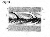
- Figs. 12 to 14 are sectional views illustrating examples of the object subjected to laser processing by this embodiment.
- the object 1 having a thickness of 100 ⁇ m is irradiated with the laser light L from the front face 3 side, so as to form the modified region 7 and the fracture C.
- the pulse width H is 150 nsec (E1 in Fig. 10 ), while the converging point P is located at 95 ⁇ m from the front face 3.
- the pulse width H is 300 nsec (E2 in Fig. 10 ), while the converging point P is located at 95 ⁇ m from the front face 3.
- the pulse width H is 400 nsec (E3 in Fig. 10 ), while the converging point P is located at 85 ⁇ m from the front face 3.
- the pulse width H is 500 nsec (E4 in Fig. 10 ), while the converging point P is located at 80 ⁇ m from the front face 3.
- the pulse width H is 550 nsec (E5 in Fig. 10 ), while the converging point P is located at 60 ⁇ m from the front face 3.
- Fig. 15 is a sectional view illustrating another example of the object to be processed subjected to laser processing by this embodiment.
- the object to be processed 1 having a thickness of 300 ⁇ m is irradiated with the laser light L from the front face 3 side, so as to form modified regions 7a, 7b, while the fracture C is generated from the modified region 7b on the upper side.
- the converging point P is located at 240 ⁇ m from the front face 3, so as to form the modified region 7a, and then at 155 ⁇ m from the front face 3, so as to form the modified region 7b.
- the pulse width H is 650 nsec (E6 in Fig. 10 ) in order to generate the fracture C as FC having the fracture length CL of 300 ⁇ m.
- Fig. 16 is a sectional view illustrating still another example of the object to be processed subjected to laser processing by the embodiment.
- the object to be processed 1 having a thickness of 600 ⁇ m is irradiated with the laser light L from the front face 3 side, so as to form modified regions 7a, 7b, while the fracture C is generated from the modified region 7b on the upper side.
- the converging point P is located at 591 ⁇ m from the front face 3, so as to form the modified region 7a, and then at 541 ⁇ m from the front face 3, so as to form the modified region 7b.
- the pulse width H is 500 nsec (E7 in Fig. 10 ) in order to generate the fracture C as BHC having the fracture length CL of 140 ⁇ m.
- the laser processing device in accordance with the present invention is not limited to the laser processing device 100 in accordance with the embodiment, but may be any of those modifying the same within a scope which does not change the gist set forth in each claim or those applying the same to others.
- the fracture length CL, the thickness of the object 1, and the pulse width of the laser light L are associated with each other so as to construct the data table Tb (see Fig. 10 ) in the above-mentioned embodiment, this is not restrictive as long as the pulse width can be changed according to the fracture length CL generated (or to be generated) from the modified region 7.
- the laser processing can be carried out in view of this thickness, whereby the fracture length CL and the pulse width of the laser light L may be associated with each other alone, so as to construct the data table Tb. That is, the pulse width can be changed according to the input value concerning the fracture length CL alone.
- the laser processing can be carried out in view of (based on) the fracture length CL, whereby the thickness of the object 1 and the pulse width of the laser light L may be associated with each other alone as illustrated in Fig. 18(a), so as to construct the data table Tb. That is, the pulse width can be changed according to the input value concerning the thickness of the object 1 alone.
- processing conditions including processing condition 1 which is a condition more concerned with the quality and processing condition 2 which is a condition more concerned with the processing speed may further be associated therewith, so as to construct the data table Tb. This can favorably respond to the making of a plurality of kinds of mass products.
- the laser processing can be carried out in view of them, whereby the position of the converging point P and the pulse width of the laser light L may be associated with each other alone as illustrated in Fig. 18(c), so as to construct the data table Tb. That is, the pulse width can be changed according to the input value concerning the position of the converging point P alone.
- the data table Tb is fed into the laser light source controller 102 beforehand in the above-mentioned embodiment but may be read by the laser light source controller 102 through a line such as the Internet.
- the object 1 may contain or comprise silicon, glass, LiTaO 3 , or sapphire (Al 2 O 3 ), for example.
- a fracture having a desirable length can be generated from a modified region.
Landscapes
- Engineering & Computer Science (AREA)
- Physics & Mathematics (AREA)
- Optics & Photonics (AREA)
- Plasma & Fusion (AREA)
- Mechanical Engineering (AREA)
- Oil, Petroleum & Natural Gas (AREA)
- Chemical Kinetics & Catalysis (AREA)
- General Chemical & Material Sciences (AREA)
- Chemical & Material Sciences (AREA)
- Condensed Matter Physics & Semiconductors (AREA)
- General Physics & Mathematics (AREA)
- Manufacturing & Machinery (AREA)
- Computer Hardware Design (AREA)
- Microelectronics & Electronic Packaging (AREA)
- Power Engineering (AREA)
- Laser Beam Processing (AREA)
- Dicing (AREA)
Applications Claiming Priority (2)
| Application Number | Priority Date | Filing Date | Title |
|---|---|---|---|
| JP2009092846 | 2009-04-07 | ||
| PCT/JP2010/055585 WO2010116917A1 (fr) | 2009-04-07 | 2010-03-29 | Dispositif d'usinage laser et procédé d'usinage laser |
Publications (2)
| Publication Number | Publication Date |
|---|---|
| EP2418041A1 true EP2418041A1 (fr) | 2012-02-15 |
| EP2418041A4 EP2418041A4 (fr) | 2017-06-21 |
Family
ID=42936202
Family Applications (1)
| Application Number | Title | Priority Date | Filing Date |
|---|---|---|---|
| EP10761616.1A Pending EP2418041A4 (fr) | 2009-04-07 | 2010-03-29 | Dispositif d'usinage laser et procédé d'usinage laser |
Country Status (7)
| Country | Link |
|---|---|
| US (1) | US9035216B2 (fr) |
| EP (1) | EP2418041A4 (fr) |
| JP (2) | JP5639997B2 (fr) |
| KR (1) | KR101769158B1 (fr) |
| CN (1) | CN102317030B (fr) |
| TW (1) | TWI593497B (fr) |
| WO (1) | WO2010116917A1 (fr) |
Families Citing this family (28)
| Publication number | Priority date | Publication date | Assignee | Title |
|---|---|---|---|---|
| JP2011201759A (ja) * | 2010-03-05 | 2011-10-13 | Namiki Precision Jewel Co Ltd | 多層膜付き単結晶基板、多層膜付き単結晶基板の製造方法および素子製造方法 |
| JP5552373B2 (ja) | 2010-06-02 | 2014-07-16 | 浜松ホトニクス株式会社 | レーザ加工方法 |
| JP5950269B2 (ja) * | 2011-02-10 | 2016-07-13 | 国立大学法人埼玉大学 | 基板加工方法及び基板 |
| CN102152003B (zh) * | 2011-02-24 | 2014-03-12 | 华中科技大学 | 双激光束分离光学晶体方法及装置 |
| JP5840215B2 (ja) * | 2011-09-16 | 2016-01-06 | 浜松ホトニクス株式会社 | レーザ加工方法及びレーザ加工装置 |
| JP2013126682A (ja) * | 2011-11-18 | 2013-06-27 | Hamamatsu Photonics Kk | レーザ加工方法 |
| KR101361777B1 (ko) * | 2012-04-03 | 2014-02-13 | 주식회사 이오테크닉스 | 레이저 가공방법 |
| JP6064519B2 (ja) * | 2012-10-29 | 2017-01-25 | 三星ダイヤモンド工業株式会社 | レーザー加工装置、および、パターン付き基板の加工条件設定方法 |
| JP6423135B2 (ja) * | 2012-11-29 | 2018-11-14 | 三星ダイヤモンド工業株式会社 | パターン付き基板の分割方法 |
| JP6208430B2 (ja) * | 2013-01-25 | 2017-10-04 | 株式会社ディスコ | レーザー加工方法 |
| JP6071775B2 (ja) * | 2013-06-26 | 2017-02-01 | 株式会社ディスコ | ウェーハの加工方法 |
| US9102007B2 (en) * | 2013-08-02 | 2015-08-11 | Rofin-Sinar Technologies Inc. | Method and apparatus for performing laser filamentation within transparent materials |
| JP6241174B2 (ja) * | 2013-09-25 | 2017-12-06 | 三星ダイヤモンド工業株式会社 | レーザー加工装置、および、パターン付き基板の加工条件設定方法 |
| CN103862180A (zh) * | 2014-01-29 | 2014-06-18 | 苏州兰叶光电科技有限公司 | 玻璃盖片激光划片装置 |
| JP2016042515A (ja) * | 2014-08-15 | 2016-03-31 | 株式会社ディスコ | ウエーハの加工方法 |
| JP2016042514A (ja) * | 2014-08-15 | 2016-03-31 | 株式会社ディスコ | ウエーハの加工方法 |
| JP2016072278A (ja) * | 2014-09-26 | 2016-05-09 | 株式会社ディスコ | ウエーハの加工方法 |
| JP2016076521A (ja) * | 2014-10-02 | 2016-05-12 | 株式会社ディスコ | ウエーハの加工方法 |
| JP6817822B2 (ja) * | 2017-01-18 | 2021-01-20 | 株式会社ディスコ | 加工方法 |
| JP7307534B2 (ja) * | 2018-10-04 | 2023-07-12 | 浜松ホトニクス株式会社 | レーザ加工方法、半導体デバイス製造方法及び検査装置 |
| US10576585B1 (en) | 2018-12-29 | 2020-03-03 | Cree, Inc. | Laser-assisted method for parting crystalline material |
| US11024501B2 (en) | 2018-12-29 | 2021-06-01 | Cree, Inc. | Carrier-assisted method for parting crystalline material along laser damage region |
| US10562130B1 (en) | 2018-12-29 | 2020-02-18 | Cree, Inc. | Laser-assisted method for parting crystalline material |
| US10611052B1 (en) | 2019-05-17 | 2020-04-07 | Cree, Inc. | Silicon carbide wafers with relaxed positive bow and related methods |
| TW202106428A (zh) * | 2019-07-18 | 2021-02-16 | 日商東京威力科創股份有限公司 | 處理裝置及處理方法 |
| JP7391583B2 (ja) * | 2019-09-18 | 2023-12-05 | 浜松ホトニクス株式会社 | 検査装置及び検査方法 |
| JP7305495B2 (ja) * | 2019-09-18 | 2023-07-10 | 浜松ホトニクス株式会社 | 検査装置及び検査方法 |
| JP7385504B2 (ja) | 2020-03-06 | 2023-11-22 | 浜松ホトニクス株式会社 | 検査装置及び処理システム |
Family Cites Families (71)
| Publication number | Priority date | Publication date | Assignee | Title |
|---|---|---|---|---|
| US4546231A (en) | 1983-11-14 | 1985-10-08 | Group Ii Manufacturing Ltd. | Creation of a parting zone in a crystal structure |
| US5073687A (en) * | 1989-06-22 | 1991-12-17 | Canon Kabushiki Kaisha | Method and apparatus for working print board by laser |
| KR0171947B1 (ko) | 1995-12-08 | 1999-03-20 | 김주용 | 반도체소자 제조를 위한 노광 방법 및 그를 이용한 노광장치 |
| JP2000288758A (ja) | 1999-03-31 | 2000-10-17 | Hitachi Ltd | レーザ切断装置 |
| US6417485B1 (en) * | 2000-05-30 | 2002-07-09 | Igor Troitski | Method and laser system controlling breakdown process development and space structure of laser radiation for production of high quality laser-induced damage images |
| JP4659300B2 (ja) | 2000-09-13 | 2011-03-30 | 浜松ホトニクス株式会社 | レーザ加工方法及び半導体チップの製造方法 |
| EP1635390B1 (fr) | 2002-03-12 | 2011-07-27 | Hamamatsu Photonics K. K. | Méthode de division de substrats |
| TWI326626B (en) | 2002-03-12 | 2010-07-01 | Hamamatsu Photonics Kk | Laser processing method |
| EP2272618B1 (fr) | 2002-03-12 | 2015-10-07 | Hamamatsu Photonics K.K. | Procédé de découpe d'objet à traiter |
| JP3667705B2 (ja) | 2002-03-26 | 2005-07-06 | 住友重機械工業株式会社 | レーザ加工装置及び加工方法 |
| TWI520269B (zh) | 2002-12-03 | 2016-02-01 | Hamamatsu Photonics Kk | Cutting method of semiconductor substrate |
| ATE550129T1 (de) | 2002-12-05 | 2012-04-15 | Hamamatsu Photonics Kk | Laserbearbeitungsvorrichtungen |
| JP2004188422A (ja) | 2002-12-06 | 2004-07-08 | Hamamatsu Photonics Kk | レーザ加工装置及びレーザ加工方法 |
| JP2004268103A (ja) * | 2003-03-10 | 2004-09-30 | Hamamatsu Photonics Kk | レーザ加工方法 |
| FR2852250B1 (fr) | 2003-03-11 | 2009-07-24 | Jean Luc Jouvin | Fourreau de protection pour canule, un ensemble d'injection comportant un tel fourreau et aiguille equipee d'un tel fourreau |
| US8685838B2 (en) | 2003-03-12 | 2014-04-01 | Hamamatsu Photonics K.K. | Laser beam machining method |
| CN1826207B (zh) | 2003-07-18 | 2010-06-16 | 浜松光子学株式会社 | 激光加工方法、激光加工装置以及加工产品 |
| JP4703983B2 (ja) * | 2003-07-18 | 2011-06-15 | 浜松ホトニクス株式会社 | 切断方法 |
| JP4563097B2 (ja) | 2003-09-10 | 2010-10-13 | 浜松ホトニクス株式会社 | 半導体基板の切断方法 |
| JP2005086175A (ja) | 2003-09-11 | 2005-03-31 | Hamamatsu Photonics Kk | 半導体薄膜の製造方法、半導体薄膜、半導体薄膜チップ、電子管、及び光検出素子 |
| GB0328370D0 (en) * | 2003-12-05 | 2004-01-14 | Southampton Photonics Ltd | Apparatus for providing optical radiation |
| WO2005067113A1 (fr) | 2004-01-07 | 2005-07-21 | Hamamatsu Photonics K.K. | Dispositif photoemetteur a semi-conducteur et son procede de fabrication |
| JP4509578B2 (ja) | 2004-01-09 | 2010-07-21 | 浜松ホトニクス株式会社 | レーザ加工方法及びレーザ加工装置 |
| JP4601965B2 (ja) | 2004-01-09 | 2010-12-22 | 浜松ホトニクス株式会社 | レーザ加工方法及びレーザ加工装置 |
| JP4598407B2 (ja) | 2004-01-09 | 2010-12-15 | 浜松ホトニクス株式会社 | レーザ加工方法及びレーザ加工装置 |
| JP4348199B2 (ja) | 2004-01-16 | 2009-10-21 | 日立ビアメカニクス株式会社 | レーザ加工方法およびレーザ加工装置 |
| JP2005268752A (ja) * | 2004-02-19 | 2005-09-29 | Canon Inc | レーザ割断方法、被割断部材および半導体素子チップ |
| JP4536407B2 (ja) | 2004-03-30 | 2010-09-01 | 浜松ホトニクス株式会社 | レーザ加工方法及び加工対象物 |
| CN100527360C (zh) | 2004-03-30 | 2009-08-12 | 浜松光子学株式会社 | 激光加工方法及半导体芯片 |
| CN1938827B (zh) | 2004-03-30 | 2010-05-26 | 浜松光子学株式会社 | 激光加工方法及半导体芯片 |
| US7804043B2 (en) * | 2004-06-15 | 2010-09-28 | Laserfacturing Inc. | Method and apparatus for dicing of thin and ultra thin semiconductor wafer using ultrafast pulse laser |
| JP4634089B2 (ja) | 2004-07-30 | 2011-02-16 | 浜松ホトニクス株式会社 | レーザ加工方法 |
| EP1775059B1 (fr) | 2004-08-06 | 2015-01-07 | Hamamatsu Photonics K.K. | Procédé de traitement laser et dispositif semi-conducteur |
| WO2006037114A2 (fr) * | 2004-09-28 | 2006-04-06 | Hitachi Via Mechanics, Ltd | Production par laser a fibre de microtrous d'interconnexion perces par laser pour applications de perçage multicouche, de decoupage en des, de detourage ou de fraisage |
| JP2006108459A (ja) | 2004-10-07 | 2006-04-20 | Disco Abrasive Syst Ltd | シリコンウエーハのレーザー加工方法およびレーザー加工装置 |
| JP4754801B2 (ja) | 2004-10-13 | 2011-08-24 | 浜松ホトニクス株式会社 | レーザ加工方法 |
| JP4917257B2 (ja) | 2004-11-12 | 2012-04-18 | 浜松ホトニクス株式会社 | レーザ加工方法 |
| JP4781661B2 (ja) | 2004-11-12 | 2011-09-28 | 浜松ホトニクス株式会社 | レーザ加工方法 |
| US8093530B2 (en) * | 2004-11-19 | 2012-01-10 | Canon Kabushiki Kaisha | Laser cutting apparatus and laser cutting method |
| JP4198123B2 (ja) | 2005-03-22 | 2008-12-17 | 浜松ホトニクス株式会社 | レーザ加工方法 |
| JP4776994B2 (ja) | 2005-07-04 | 2011-09-21 | 浜松ホトニクス株式会社 | 加工対象物切断方法 |
| JP4395110B2 (ja) * | 2005-07-29 | 2010-01-06 | 東レエンジニアリング株式会社 | 透明材料へのマーキング方法およびこれを用いた装置 |
| JP4749799B2 (ja) | 2005-08-12 | 2011-08-17 | 浜松ホトニクス株式会社 | レーザ加工方法 |
| JP2007079161A (ja) | 2005-09-14 | 2007-03-29 | Toyota Motor Corp | 超短パルスレーザー加工用光学系、材料微細加工方法、及び微細加工装置 |
| JP4762653B2 (ja) | 2005-09-16 | 2011-08-31 | 浜松ホトニクス株式会社 | レーザ加工方法及びレーザ加工装置 |
| JP4237745B2 (ja) | 2005-11-18 | 2009-03-11 | 浜松ホトニクス株式会社 | レーザ加工方法 |
| JP4907965B2 (ja) | 2005-11-25 | 2012-04-04 | 浜松ホトニクス株式会社 | レーザ加工方法 |
| JP4804911B2 (ja) | 2005-12-22 | 2011-11-02 | 浜松ホトニクス株式会社 | レーザ加工装置 |
| JP4907984B2 (ja) | 2005-12-27 | 2012-04-04 | 浜松ホトニクス株式会社 | レーザ加工方法及び半導体チップ |
| JP4322881B2 (ja) * | 2006-03-14 | 2009-09-02 | 浜松ホトニクス株式会社 | レーザ加工方法及びレーザ加工装置 |
| US20070228023A1 (en) * | 2006-03-30 | 2007-10-04 | Klaus Kleine | Pulsed Synchronized Laser Cutting of Stents |
| JP5183892B2 (ja) | 2006-07-03 | 2013-04-17 | 浜松ホトニクス株式会社 | レーザ加工方法 |
| US7897487B2 (en) | 2006-07-03 | 2011-03-01 | Hamamatsu Photonics K.K. | Laser processing method and chip |
| US7732731B2 (en) * | 2006-09-15 | 2010-06-08 | Gsi Group Corporation | Method and system for laser processing targets of different types on a workpiece |
| JP4954653B2 (ja) | 2006-09-19 | 2012-06-20 | 浜松ホトニクス株式会社 | レーザ加工方法 |
| KR101428823B1 (ko) | 2006-09-19 | 2014-08-11 | 하마마츠 포토닉스 가부시키가이샤 | 레이저 가공 방법 및 레이저 가공 장치 |
| JP5101073B2 (ja) | 2006-10-02 | 2012-12-19 | 浜松ホトニクス株式会社 | レーザ加工装置 |
| JP4964554B2 (ja) | 2006-10-03 | 2012-07-04 | 浜松ホトニクス株式会社 | レーザ加工方法 |
| JP5132911B2 (ja) | 2006-10-03 | 2013-01-30 | 浜松ホトニクス株式会社 | レーザ加工方法 |
| EP2070636B1 (fr) | 2006-10-04 | 2015-08-05 | Hamamatsu Photonics K.K. | Procédé de traitement laser |
| JP2008212998A (ja) | 2007-03-06 | 2008-09-18 | Seiko Epson Corp | レーザ加工装置、レーザ加工方法、基板の分割方法、及び電気光学装置の製造方法 |
| JP2008276057A (ja) * | 2007-05-02 | 2008-11-13 | Active Inc | 液晶表示装置の透明電極膜加工方法 |
| JP5336054B2 (ja) | 2007-07-18 | 2013-11-06 | 浜松ホトニクス株式会社 | 加工情報供給装置を備える加工情報供給システム |
| JP5139739B2 (ja) | 2007-07-19 | 2013-02-06 | パナソニック株式会社 | 積層体の割断方法 |
| JP4402708B2 (ja) | 2007-08-03 | 2010-01-20 | 浜松ホトニクス株式会社 | レーザ加工方法、レーザ加工装置及びその製造方法 |
| JP5225639B2 (ja) | 2007-09-06 | 2013-07-03 | 浜松ホトニクス株式会社 | 半導体レーザ素子の製造方法 |
| JP5342772B2 (ja) | 2007-10-12 | 2013-11-13 | 浜松ホトニクス株式会社 | 加工対象物切断方法 |
| JP5449665B2 (ja) | 2007-10-30 | 2014-03-19 | 浜松ホトニクス株式会社 | レーザ加工方法 |
| JP5134928B2 (ja) | 2007-11-30 | 2013-01-30 | 浜松ホトニクス株式会社 | 加工対象物研削方法 |
| JP5054496B2 (ja) | 2007-11-30 | 2012-10-24 | 浜松ホトニクス株式会社 | 加工対象物切断方法 |
| JP5241525B2 (ja) | 2009-01-09 | 2013-07-17 | 浜松ホトニクス株式会社 | レーザ加工装置 |
-
2010
- 2010-03-29 JP JP2011508335A patent/JP5639997B2/ja active Active
- 2010-03-29 KR KR1020117013931A patent/KR101769158B1/ko active IP Right Grant
- 2010-03-29 WO PCT/JP2010/055585 patent/WO2010116917A1/fr active Application Filing
- 2010-03-29 US US13/262,995 patent/US9035216B2/en active Active
- 2010-03-29 CN CN201080008067.XA patent/CN102317030B/zh active Active
- 2010-03-29 EP EP10761616.1A patent/EP2418041A4/fr active Pending
- 2010-04-06 TW TW099110584A patent/TWI593497B/zh active
-
2014
- 2014-04-22 JP JP2014088207A patent/JP2014176901A/ja active Pending
Non-Patent Citations (1)
| Title |
|---|
| See references of WO2010116917A1 * |
Also Published As
| Publication number | Publication date |
|---|---|
| WO2010116917A1 (fr) | 2010-10-14 |
| TWI593497B (zh) | 2017-08-01 |
| CN102317030B (zh) | 2014-08-20 |
| EP2418041A4 (fr) | 2017-06-21 |
| US20120103948A1 (en) | 2012-05-03 |
| KR20120005432A (ko) | 2012-01-16 |
| JPWO2010116917A1 (ja) | 2012-10-18 |
| JP5639997B2 (ja) | 2014-12-10 |
| TW201043382A (en) | 2010-12-16 |
| JP2014176901A (ja) | 2014-09-25 |
| KR101769158B1 (ko) | 2017-08-17 |
| CN102317030A (zh) | 2012-01-11 |
| US9035216B2 (en) | 2015-05-19 |
Similar Documents
| Publication | Publication Date | Title |
|---|---|---|
| US9035216B2 (en) | Method and device for controlling interior fractures by controlling the laser pulse width | |
| CN102481666B (zh) | 激光加工方法及芯片 | |
| KR101349556B1 (ko) | 레이저 가공 방법 및 레이저 가공 장치 | |
| EP2070636B1 (fr) | Procédé de traitement laser | |
| US9012805B2 (en) | Laser working method | |
| US8890027B2 (en) | Laser processing method and laser processing system | |
| EP2070634B1 (fr) | Dispositif de traitement laser | |
| JP5597052B2 (ja) | レーザ加工方法 | |
| EP2070635B1 (fr) | Procédé de traitement laser | |
| US9076855B2 (en) | Laser machining method | |
| EP1867427A1 (fr) | Procede d usinage au laser | |
| JP2009106977A (ja) | レーザ加工方法 | |
| TWI515071B (zh) | Laser processing method | |
| US20150298252A1 (en) | Laser machining method and laser machining device | |
| JP5117806B2 (ja) | レーザ加工方法及びレーザ加工装置 |
Legal Events
| Date | Code | Title | Description |
|---|---|---|---|
| PUAI | Public reference made under article 153(3) epc to a published international application that has entered the european phase |
Free format text: ORIGINAL CODE: 0009012 |
|
| 17P | Request for examination filed |
Effective date: 20111104 |
|
| AK | Designated contracting states |
Kind code of ref document: A1 Designated state(s): AT BE BG CH CY CZ DE DK EE ES FI FR GB GR HR HU IE IS IT LI LT LU LV MC MK MT NL NO PL PT RO SE SI SK SM TR |
|
| DAX | Request for extension of the european patent (deleted) | ||
| RA4 | Supplementary search report drawn up and despatched (corrected) |
Effective date: 20170522 |
|
| RIC1 | Information provided on ipc code assigned before grant |
Ipc: H01L 21/301 20060101ALI20170516BHEP Ipc: B23K 26/53 20140101ALI20170516BHEP Ipc: B23K 26/40 20140101ALI20170516BHEP Ipc: B23K 26/00 20140101ALI20170516BHEP Ipc: B23K 26/36 20140101AFI20170516BHEP Ipc: B23K 103/00 20060101ALI20170516BHEP |
|
| STAA | Information on the status of an ep patent application or granted ep patent |
Free format text: STATUS: EXAMINATION IS IN PROGRESS |
|
| 17Q | First examination report despatched |
Effective date: 20200506 |
|
| STAA | Information on the status of an ep patent application or granted ep patent |
Free format text: STATUS: EXAMINATION IS IN PROGRESS |
|
| STAA | Information on the status of an ep patent application or granted ep patent |
Free format text: STATUS: EXAMINATION IS IN PROGRESS |
|
| GRAP | Despatch of communication of intention to grant a patent |
Free format text: ORIGINAL CODE: EPIDOSNIGR1 |
|
| STAA | Information on the status of an ep patent application or granted ep patent |
Free format text: STATUS: GRANT OF PATENT IS INTENDED |
|
| INTG | Intention to grant announced |
Effective date: 20240502 |