EP2269765B1 - Chip semiconducteur découpé - Google Patents
Chip semiconducteur découpé Download PDFInfo
- Publication number
- EP2269765B1 EP2269765B1 EP10009404.4A EP10009404A EP2269765B1 EP 2269765 B1 EP2269765 B1 EP 2269765B1 EP 10009404 A EP10009404 A EP 10009404A EP 2269765 B1 EP2269765 B1 EP 2269765B1
- Authority
- EP
- European Patent Office
- Prior art keywords
- machining target
- machining
- laser light
- area
- minute
- Prior art date
- Legal status (The legal status is an assumption and is not a legal conclusion. Google has not performed a legal analysis and makes no representation as to the accuracy of the status listed.)
- Active
Links
- 239000004065 semiconductor Substances 0.000 title claims description 37
- 238000005520 cutting process Methods 0.000 claims description 67
- XUIMIQQOPSSXEZ-UHFFFAOYSA-N Silicon Chemical compound [Si] XUIMIQQOPSSXEZ-UHFFFAOYSA-N 0.000 claims description 58
- 229910052710 silicon Inorganic materials 0.000 claims description 56
- 239000010703 silicon Substances 0.000 claims description 56
- 239000000758 substrate Substances 0.000 claims description 13
- 238000003754 machining Methods 0.000 description 165
- 235000012431 wafers Nutrition 0.000 description 59
- 238000000034 method Methods 0.000 description 35
- 238000010521 absorption reaction Methods 0.000 description 15
- 238000005259 measurement Methods 0.000 description 14
- 238000009826 distribution Methods 0.000 description 9
- 238000002844 melting Methods 0.000 description 9
- 230000008018 melting Effects 0.000 description 9
- 230000003287 optical effect Effects 0.000 description 9
- 230000002093 peripheral effect Effects 0.000 description 9
- 238000010586 diagram Methods 0.000 description 6
- 239000000463 material Substances 0.000 description 6
- 229910021417 amorphous silicon Inorganic materials 0.000 description 5
- 150000001875 compounds Chemical class 0.000 description 5
- 238000001069 Raman spectroscopy Methods 0.000 description 4
- 239000013078 crystal Substances 0.000 description 4
- 230000000694 effects Effects 0.000 description 3
- 230000005684 electric field Effects 0.000 description 3
- 230000001678 irradiating effect Effects 0.000 description 3
- 229910017502 Nd:YVO4 Inorganic materials 0.000 description 2
- RTAQQCXQSZGOHL-UHFFFAOYSA-N Titanium Chemical compound [Ti] RTAQQCXQSZGOHL-UHFFFAOYSA-N 0.000 description 2
- 238000004458 analytical method Methods 0.000 description 2
- 230000015572 biosynthetic process Effects 0.000 description 2
- 230000006835 compression Effects 0.000 description 2
- 238000007906 compression Methods 0.000 description 2
- 238000001514 detection method Methods 0.000 description 2
- 238000003384 imaging method Methods 0.000 description 2
- 239000002994 raw material Substances 0.000 description 2
- 238000000926 separation method Methods 0.000 description 2
- 229910001218 Gallium arsenide Inorganic materials 0.000 description 1
- 230000004075 alteration Effects 0.000 description 1
- 238000005452 bending Methods 0.000 description 1
- 229910052799 carbon Inorganic materials 0.000 description 1
- 238000003776 cleavage reaction Methods 0.000 description 1
- 239000000470 constituent Substances 0.000 description 1
- 229910003460 diamond Inorganic materials 0.000 description 1
- 239000010432 diamond Substances 0.000 description 1
- 230000005284 excitation Effects 0.000 description 1
- 239000011521 glass Substances 0.000 description 1
- 239000012535 impurity Substances 0.000 description 1
- 239000004973 liquid crystal related substance Substances 0.000 description 1
- 238000004519 manufacturing process Methods 0.000 description 1
- 230000003252 repetitive effect Effects 0.000 description 1
- 239000000523 sample Substances 0.000 description 1
- 230000007017 scission Effects 0.000 description 1
- 238000001228 spectrum Methods 0.000 description 1
Images


Classifications
-
- H—ELECTRICITY
- H01—ELECTRIC ELEMENTS
- H01S—DEVICES USING THE PROCESS OF LIGHT AMPLIFICATION BY STIMULATED EMISSION OF RADIATION [LASER] TO AMPLIFY OR GENERATE LIGHT; DEVICES USING STIMULATED EMISSION OF ELECTROMAGNETIC RADIATION IN WAVE RANGES OTHER THAN OPTICAL
- H01S3/00—Lasers, i.e. devices using stimulated emission of electromagnetic radiation in the infrared, visible or ultraviolet wave range
- H01S3/10—Controlling the intensity, frequency, phase, polarisation or direction of the emitted radiation, e.g. switching, gating, modulating or demodulating
-
- B—PERFORMING OPERATIONS; TRANSPORTING
- B23—MACHINE TOOLS; METAL-WORKING NOT OTHERWISE PROVIDED FOR
- B23K—SOLDERING OR UNSOLDERING; WELDING; CLADDING OR PLATING BY SOLDERING OR WELDING; CUTTING BY APPLYING HEAT LOCALLY, e.g. FLAME CUTTING; WORKING BY LASER BEAM
- B23K26/00—Working by laser beam, e.g. welding, cutting or boring
- B23K26/02—Positioning or observing the workpiece, e.g. with respect to the point of impact; Aligning, aiming or focusing the laser beam
- B23K26/03—Observing, e.g. monitoring, the workpiece
- B23K26/032—Observing, e.g. monitoring, the workpiece using optical means
-
- B—PERFORMING OPERATIONS; TRANSPORTING
- B23—MACHINE TOOLS; METAL-WORKING NOT OTHERWISE PROVIDED FOR
- B23K—SOLDERING OR UNSOLDERING; WELDING; CLADDING OR PLATING BY SOLDERING OR WELDING; CUTTING BY APPLYING HEAT LOCALLY, e.g. FLAME CUTTING; WORKING BY LASER BEAM
- B23K26/00—Working by laser beam, e.g. welding, cutting or boring
- B23K26/0006—Working by laser beam, e.g. welding, cutting or boring taking account of the properties of the material involved
-
- B—PERFORMING OPERATIONS; TRANSPORTING
- B23—MACHINE TOOLS; METAL-WORKING NOT OTHERWISE PROVIDED FOR
- B23K—SOLDERING OR UNSOLDERING; WELDING; CLADDING OR PLATING BY SOLDERING OR WELDING; CUTTING BY APPLYING HEAT LOCALLY, e.g. FLAME CUTTING; WORKING BY LASER BEAM
- B23K26/00—Working by laser beam, e.g. welding, cutting or boring
- B23K26/02—Positioning or observing the workpiece, e.g. with respect to the point of impact; Aligning, aiming or focusing the laser beam
- B23K26/03—Observing, e.g. monitoring, the workpiece
-
- B—PERFORMING OPERATIONS; TRANSPORTING
- B23—MACHINE TOOLS; METAL-WORKING NOT OTHERWISE PROVIDED FOR
- B23K—SOLDERING OR UNSOLDERING; WELDING; CLADDING OR PLATING BY SOLDERING OR WELDING; CUTTING BY APPLYING HEAT LOCALLY, e.g. FLAME CUTTING; WORKING BY LASER BEAM
- B23K26/00—Working by laser beam, e.g. welding, cutting or boring
- B23K26/02—Positioning or observing the workpiece, e.g. with respect to the point of impact; Aligning, aiming or focusing the laser beam
- B23K26/06—Shaping the laser beam, e.g. by masks or multi-focusing
- B23K26/062—Shaping the laser beam, e.g. by masks or multi-focusing by direct control of the laser beam
- B23K26/0622—Shaping the laser beam, e.g. by masks or multi-focusing by direct control of the laser beam by shaping pulses
-
- B—PERFORMING OPERATIONS; TRANSPORTING
- B23—MACHINE TOOLS; METAL-WORKING NOT OTHERWISE PROVIDED FOR
- B23K—SOLDERING OR UNSOLDERING; WELDING; CLADDING OR PLATING BY SOLDERING OR WELDING; CUTTING BY APPLYING HEAT LOCALLY, e.g. FLAME CUTTING; WORKING BY LASER BEAM
- B23K26/00—Working by laser beam, e.g. welding, cutting or boring
- B23K26/02—Positioning or observing the workpiece, e.g. with respect to the point of impact; Aligning, aiming or focusing the laser beam
- B23K26/06—Shaping the laser beam, e.g. by masks or multi-focusing
- B23K26/064—Shaping the laser beam, e.g. by masks or multi-focusing by means of optical elements, e.g. lenses, mirrors or prisms
- B23K26/0643—Shaping the laser beam, e.g. by masks or multi-focusing by means of optical elements, e.g. lenses, mirrors or prisms comprising mirrors
-
- B—PERFORMING OPERATIONS; TRANSPORTING
- B23—MACHINE TOOLS; METAL-WORKING NOT OTHERWISE PROVIDED FOR
- B23K—SOLDERING OR UNSOLDERING; WELDING; CLADDING OR PLATING BY SOLDERING OR WELDING; CUTTING BY APPLYING HEAT LOCALLY, e.g. FLAME CUTTING; WORKING BY LASER BEAM
- B23K26/00—Working by laser beam, e.g. welding, cutting or boring
- B23K26/02—Positioning or observing the workpiece, e.g. with respect to the point of impact; Aligning, aiming or focusing the laser beam
- B23K26/06—Shaping the laser beam, e.g. by masks or multi-focusing
- B23K26/0665—Shaping the laser beam, e.g. by masks or multi-focusing by beam condensation on the workpiece, e.g. for focusing
-
- B—PERFORMING OPERATIONS; TRANSPORTING
- B23—MACHINE TOOLS; METAL-WORKING NOT OTHERWISE PROVIDED FOR
- B23K—SOLDERING OR UNSOLDERING; WELDING; CLADDING OR PLATING BY SOLDERING OR WELDING; CUTTING BY APPLYING HEAT LOCALLY, e.g. FLAME CUTTING; WORKING BY LASER BEAM
- B23K26/00—Working by laser beam, e.g. welding, cutting or boring
- B23K26/36—Removing material
- B23K26/361—Removing material for deburring or mechanical trimming
-
- B—PERFORMING OPERATIONS; TRANSPORTING
- B23—MACHINE TOOLS; METAL-WORKING NOT OTHERWISE PROVIDED FOR
- B23K—SOLDERING OR UNSOLDERING; WELDING; CLADDING OR PLATING BY SOLDERING OR WELDING; CUTTING BY APPLYING HEAT LOCALLY, e.g. FLAME CUTTING; WORKING BY LASER BEAM
- B23K26/00—Working by laser beam, e.g. welding, cutting or boring
- B23K26/36—Removing material
- B23K26/38—Removing material by boring or cutting
-
- B—PERFORMING OPERATIONS; TRANSPORTING
- B23—MACHINE TOOLS; METAL-WORKING NOT OTHERWISE PROVIDED FOR
- B23K—SOLDERING OR UNSOLDERING; WELDING; CLADDING OR PLATING BY SOLDERING OR WELDING; CUTTING BY APPLYING HEAT LOCALLY, e.g. FLAME CUTTING; WORKING BY LASER BEAM
- B23K26/00—Working by laser beam, e.g. welding, cutting or boring
- B23K26/36—Removing material
- B23K26/40—Removing material taking account of the properties of the material involved
- B23K26/402—Removing material taking account of the properties of the material involved involving non-metallic material, e.g. isolators
-
- B—PERFORMING OPERATIONS; TRANSPORTING
- B23—MACHINE TOOLS; METAL-WORKING NOT OTHERWISE PROVIDED FOR
- B23K—SOLDERING OR UNSOLDERING; WELDING; CLADDING OR PLATING BY SOLDERING OR WELDING; CUTTING BY APPLYING HEAT LOCALLY, e.g. FLAME CUTTING; WORKING BY LASER BEAM
- B23K26/00—Working by laser beam, e.g. welding, cutting or boring
- B23K26/50—Working by transmitting the laser beam through or within the workpiece
- B23K26/53—Working by transmitting the laser beam through or within the workpiece for modifying or reforming the material inside the workpiece, e.g. for producing break initiation cracks
-
- B—PERFORMING OPERATIONS; TRANSPORTING
- B23—MACHINE TOOLS; METAL-WORKING NOT OTHERWISE PROVIDED FOR
- B23K—SOLDERING OR UNSOLDERING; WELDING; CLADDING OR PLATING BY SOLDERING OR WELDING; CUTTING BY APPLYING HEAT LOCALLY, e.g. FLAME CUTTING; WORKING BY LASER BEAM
- B23K26/00—Working by laser beam, e.g. welding, cutting or boring
- B23K26/50—Working by transmitting the laser beam through or within the workpiece
- B23K26/55—Working by transmitting the laser beam through or within the workpiece for creating voids inside the workpiece, e.g. for forming flow passages or flow patterns
-
- B—PERFORMING OPERATIONS; TRANSPORTING
- B28—WORKING CEMENT, CLAY, OR STONE
- B28D—WORKING STONE OR STONE-LIKE MATERIALS
- B28D1/00—Working stone or stone-like materials, e.g. brick, concrete or glass, not provided for elsewhere; Machines, devices, tools therefor
- B28D1/22—Working stone or stone-like materials, e.g. brick, concrete or glass, not provided for elsewhere; Machines, devices, tools therefor by cutting, e.g. incising
- B28D1/221—Working stone or stone-like materials, e.g. brick, concrete or glass, not provided for elsewhere; Machines, devices, tools therefor by cutting, e.g. incising by thermic methods
-
- B—PERFORMING OPERATIONS; TRANSPORTING
- B28—WORKING CEMENT, CLAY, OR STONE
- B28D—WORKING STONE OR STONE-LIKE MATERIALS
- B28D5/00—Fine working of gems, jewels, crystals, e.g. of semiconductor material; apparatus or devices therefor
- B28D5/0005—Fine working of gems, jewels, crystals, e.g. of semiconductor material; apparatus or devices therefor by breaking, e.g. dicing
- B28D5/0011—Fine working of gems, jewels, crystals, e.g. of semiconductor material; apparatus or devices therefor by breaking, e.g. dicing with preliminary treatment, e.g. weakening by scoring
-
- B—PERFORMING OPERATIONS; TRANSPORTING
- B23—MACHINE TOOLS; METAL-WORKING NOT OTHERWISE PROVIDED FOR
- B23K—SOLDERING OR UNSOLDERING; WELDING; CLADDING OR PLATING BY SOLDERING OR WELDING; CUTTING BY APPLYING HEAT LOCALLY, e.g. FLAME CUTTING; WORKING BY LASER BEAM
- B23K2101/00—Articles made by soldering, welding or cutting
- B23K2101/36—Electric or electronic devices
- B23K2101/40—Semiconductor devices
-
- B—PERFORMING OPERATIONS; TRANSPORTING
- B23—MACHINE TOOLS; METAL-WORKING NOT OTHERWISE PROVIDED FOR
- B23K—SOLDERING OR UNSOLDERING; WELDING; CLADDING OR PLATING BY SOLDERING OR WELDING; CUTTING BY APPLYING HEAT LOCALLY, e.g. FLAME CUTTING; WORKING BY LASER BEAM
- B23K2103/00—Materials to be soldered, welded or cut
- B23K2103/50—Inorganic material, e.g. metals, not provided for in B23K2103/02 – B23K2103/26
- B23K2103/56—Inorganic material, e.g. metals, not provided for in B23K2103/02 – B23K2103/26 semiconducting
-
- Y—GENERAL TAGGING OF NEW TECHNOLOGICAL DEVELOPMENTS; GENERAL TAGGING OF CROSS-SECTIONAL TECHNOLOGIES SPANNING OVER SEVERAL SECTIONS OF THE IPC; TECHNICAL SUBJECTS COVERED BY FORMER USPC CROSS-REFERENCE ART COLLECTIONS [XRACs] AND DIGESTS
- Y10—TECHNICAL SUBJECTS COVERED BY FORMER USPC
- Y10T—TECHNICAL SUBJECTS COVERED BY FORMER US CLASSIFICATION
- Y10T428/00—Stock material or miscellaneous articles
- Y10T428/24—Structurally defined web or sheet [e.g., overall dimension, etc.]
- Y10T428/24479—Structurally defined web or sheet [e.g., overall dimension, etc.] including variation in thickness
Definitions
- the present invention relates to a semi conductor chip according to the preamble of claim 1 (see, for example, WO 02/22301 ).
- Non-Patent Document 1 discloses a method for cutting a machining target by laser beam machining.
- the laser beam machining method described in the Non-Patent Document 1 aims to cut silicon wafers, and it uses light having a wavelength of about 1 ⁇ m which can transmit through silicon. The light is converged to the inside of the wafer to continuously form a modifying layer, and the wafer is cut with formation of the modifying layer as a trigger.
- Non-Patent Document 1 " LASER LIGHT DICING MACHINING IN SEMICONDUCTOR WAFER” authored by Kazunao Arai, Journal of The Society of Grinding Engineers, Vol. 47, No. 5, 2003 May. pp. 229-231 .
- the present invention has an object to provide a laser beam machining method and a laser beam machining apparatus which can easily cut a machining target, and to provide a laser beam machined product which is cut easily.
- the machining target is a semiconductor substrate
- the treated area is a molten processed area. Because of irradiating laser light to the semiconductor substrate, the melting area and the minute cavity are formed.
- the minute cavities are formed along the planned cutting line, each of the minute cavities are separated. Because of separating the minute cavities, the minute cavity can be formed more efficiently.
- the laser beam machining method will be described.
- a treated area (molten processed area) is formed by multiphoton absorption, and also a minute cavity whose periphery is not substantially varied in crystal structure is formed at a predetermined position corresponding to the treated area.
- the multiphoton absorption is a phenomenon occurring when the intensity of laser light is strong. First, the multiphoton absorption will be briefly described.
- the peak power density is determined by dividing (the energy per one pulse of laser light at a focusing point) by (the beam spot sectional area of the laser light x pulse width).
- the intensity of laser light is determined by the electric field intensity (W/cm 2 ) of the laser light at a focusing point.
- Fig. 1 is a plan view showing a machining target 1 (semiconductor substrate) in a laser beam machining process
- Fig. 2 is a cross-sectional view of the machining target 1 shown in Fig. 1 , which is taken along a II-II line
- Fig. 3 is a plan view showing the machining target 1 after the laser beam machining process
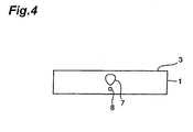
- Fig. 4 is a cross-sectional view of the machining target 1 shown in Fig. 3 , which is taken along a IV-IV line
- Fig. 5 is a cross-sectional view of the machining target 1 shown in Fig. 3 , which is taken along a V-V line
- Fig. 6 is a plan view of the machining target 1 which is cut.
- a planned cutting line 5 is drawn on the surface 3 of the machining target 1.
- the planned cutting line 5 is a linearly-extending virtual line.
- the laser beam machining method according to this embodiment matches a focus point F to the inside of the machining target 1 under a condition where multiphoton occurs, and irradiates laser light L to the machining target 1 to form a treated area 7.
- the focusing point means a portion to which the laser light L is focused.
- the laser light L is relatively moved along the planned cutting line 5 (that is, along a direction of an arrow A) at a predetermined pitch P to thereby move the focus point F along the planned cutting line 5, whereby a modified area comprising a treated area 7 and a minute cavity is formed along the planned cutting line 5 only inside the machining target 1 as shown in Fig. 3 to Fig. 5 .
- the treated area 7 and the minute cavity 8 are formed at the predetermined pitch P at which the laser light L is moved as shown in Fig. 5 .
- This pitch P is equal to pulse pitch of laser light L.
- the minute cavity 8 is formed at machining depth C, in thickness B of the machining target 1. As shown in Fig.
- the minute cavity 8 is formed at the opposite side to the treated area 7 when viewing in the irradiation direction of the laser light L.
- the treated area 7 and the minute cavity 8 may be formed continuously with each other even when the treated area 7 and the minute cavity 8 are spaced from each other at a predetermined interval.
- the treated area 7 is formed not by making the machining target 1 absorb the laser light L to heat the machining target 1, but by transmitting the laser light L through the machining target 1 to induce multiphoton absorption inside the machining target 1. Accordingly, the laser light L is hardly absorbed on the surface 3 of the machining target 1, and thus the surface 3 of the machining target 1 is not melted.
- the machining target 1 can be cut by forming the treated area 7 and the minute cavity 8 in the machining target 1 to obtain a laser beam machined object as described above, attaching tape on the back side of the machining target 1 and then detaching the tape in a direction perpendicular to the planned cutting line 5 of the machining target 1 (see Fig. 6 ).
- the machining target 1 is broken from the cut starting point, and thus the machining target 1 can be cut with relatively small force as shown in Fig. 6 . Accordingly, the machining target 1 can be cut without generating any unnecessary cracks (namely, cracks which run off the planned cutting line) on the surface 3 of the machining target 1.
- a molten processed area is known as one of the treated areas formed by multiphoton absorption in this embodiment.
- the laser light is converged to the inside of the machining target (for example, a semiconductor material such as silicon wafer or the like), and irradiated under the condition where electric field intensity at the focusing point is equal to 1 x 10 8 (W/cm 2 ) or more and the pulse width is equal to 1 ⁇ s or less, whereby the inside of the machining target is locally heated by multiphoton absorption.
- a molten processed area is formed inside the machining target by the heat.
- the molten processed area means at least one of an area which has been once melted and then re-solidified, an area under a melting state and an area which was melted and is now being re-solidified. Furthermore, the molten processed area may be called a phase-varied area or a crystal-structure varied area. Still further, the molten processed area may be called an area in which one of a monocrystal structure, an amorphous structure and a polycrystal structure is varied with another structure.
- the molten processed area means an area varied from the monocrystal structure to the monocrystal structure, an area varied from the monocrystal structure to the polycrystal structure or an area varied from the monocrystal structure to a structure containing the amorphous structure and the polycrystal structure.
- the machining target has a silicon monocrystal structure, than the molten processed area means an amorphous silicon structure, for example.
- the upper limit value of the electric field intensity is equal to 1 ⁇ 10 12 (W/cm 2 ), for example.
- the pulse width is preferably set to 1ns to 200ns, for example.
- the minute cavity formed means an area around which the crystal structure is not substantially varied.
- the peripheral portion of the minute cavity retains the silicon monocrystal structure.
- Fig. 7 shows a laser beam machining apparatus 100 using the laser beam machining method.
- the laser beam machining apparatus 100 shown in Fig. 7 is equipped with laser light source 101 for generating laser light L, laser light source controller 102 for controlling the laser light source 101 for adjusting the output, pulse width, etc., of the laser light L, a dichroic mirror 103 which has a function of reflecting the laser light and is disposed so that the direction of the optical axis of the laser light L is varied by 90 degrees, a condenser lens 105 for converging the laser light L reflected from the dichroic mirror 103, a mount table 107 for mounting thereon the machining target 1 to which the laser light L converged by the condenser lens 105 is irradiated, an X-axis stage 109 (controller) for moving the mount table 107 in the X-axis direction, a Y-axis stage 111 (controller) for moving the mount table 107 in a Y-axis direction perpendicular to the X-axis direction, a Z-axis stage 113 (controller)
- machining target 1 is a silicon wafer, and thus expand tape 106 is attached to the back side of the machining target 1.
- the Z-axis direction is perpendicular to the surface 3 of the machining target 1, it corresponds to the focal depth direction of the laser light L made incident to the machining target 1. Accordingly, the focus point F of the laser light L can be positioned at the inside of the machining target 1 by moving the Z-axis stage 113 in the Z-axis direction.
- the movement of the focus point F in the X(Y)-axis direction is carried out by moving the machining target 1 in the X(Y) axis direction with the X(Y)-axis stage 109 (111).
- the X(Y)-axis stage 109 (111) is an example of moving means.
- the laser light source 101 is an Nd:YAG laser for emitting a pulse laser light.
- An Nd:YVO 4 laser, an Nd:YLF laser or a titan sapphire laser may be also used as the laser light source 101.
- the treated area is a molten processed portion
- the Nd:YAG laser, the Nd:YVO 4 laser or the Nd:YLF laser is preferably used.
- the titan sapphire laser is preferably used.
- Pulse laser light is used to machine the machining target 1, however, continuous wave laser light may be used insofar as it can induce multiphoton absorption.
- the term of the laser light is broadly defined to contain a laser beam.
- the condenser lens 105 is an example of light converging means.
- the Z-axis stage 113 is an example of means for positioning the focus point of the laser light at the inside of the machining target.
- the focus point of the laser light may be also positioned at the inside of the machining target by moving the condenser lens 105 in the Z-axis direction.
- the laser beam machining apparatus 100 is further equipped with an observing light source 117 for generating visible light to irradiate visible light to the machining target 1 mounted on the mount table 107, and a visible-light beam splitter 119 disposed on the same optical axis as the dichroic mirror 103 and the condenser lens 105.
- the dichroic mirror 103 is disposed between the beam splitter 119 and the condenser lens 105.
- the beam splitter 119 has a function of reflecting about a half of visible light and transmitting therethrough the other half of the visible light, and is disposed to vary the direction of the optical axis of the visible light by 90 degrees.
- the laser beam machining apparatus 100 is further equipped with a beam splitter 119, and an image pickup element 121 and an imaging lens 123 which are disposed on the same optical axis as the dichroic mirror 103 and the condenser lens 105.
- a CCD (charge-coupled device) camera is known as the image pickup element 121. Reflection light of visible light irradiated to the surface 3 containing the planned cutting line 5, etc., is transmitted through the condenser lens 105, the diachronic mirror 103 and the beam splitter 119, imaged on the imaging lens 123 and then picked up by the image pickup element 121 to obtain image pickup data.
- the laser beam machining apparatus 100 is further equipped with an image pickup data processor 125 to which the image pickup data output from the image pickup element 121 are input, an overall controller 127 for controlling the whole of the laser beam machining apparatus 100, and a monitor 129.
- the image pickup data processor 125 calculates focus point data to which the focus point of visible light generated by the observing light source 117 is positioned on the basis of the image pickup data.
- the stage controller 115 controls the movement of the Z-axis stage 113 on the basis of the focus point data so that the focus point of the visible light is positioned at the surface 3. Accordingly, the image pickup data processor 125 calculates as an auto focus unit.
- the image pickup data processor 125 calculates image data such as an enlarged image of the surface 3 or the like on the basis of the image pickup data.
- the image data are transmitted to the overall controller 127 to be subjected to various kinds of processing in the overall controller, and then transmitted to a monitor 129, whereby an enlarged image or the like is displayed on the monitor 129.
- the overall controller 127 is supplied with data from the stage controller 115, image data from the image pickup data processor 125, etc., to control the laser light source controller 102, the observing light source 117 and the stage controller 115 on the basis of these data, thereby controlling the whole of the laser beam machining apparatus 100. Therefore, the overall controller 127 functions as a computer unit.
- Fig. 8 is a flowchart showing the laser beam machining method.
- the machining target 1 is a silicon wafer.
- the optical absorption characteristic of the machining target 1 is measured by a spectrophotometer (not shown).
- a laser light source 101 for generating laser light L having a wavelength which is transparent to the machining target 1 or is slightly absorbed by the machining target 1 is selected on the basis of this measurement result (S101).
- the thickness of the machining target 1 is measured.
- a movement amount of the machining target 1 in the Z-axis direction is determined on the basis of the measurement result of the thickness and the refractive index of the machining target 1 (S103).
- This movement amount corresponds to a movement amount of the machining target 1 in the z-axis direction with respect to the focus point of the laser light L located at the surface 3 of the machining target 1 in order to position the focus point F of the laser light L at the inside of the machining target 1.
- This movement amount is input to the overall controller 127.
- the machining target 1 is mounted on the mount table 107 of the laser beam machining apparatus 100, and then visible light is emitted from the observing light source 117 to irradiate the visible light to the machining target 1 (S105).
- An image of the surface 3 of the machining target 1 containing the planned cutting line 5 thus irradiated is picked up by the image pickup element 121.
- the image pickup data thus obtained are transmitted to the image pickup data processor 125.
- the image pickup data processor 125 calculates focus data on the basis of the image pickup data so that the focus point of the visible light of the observing light source 117 is located at the surface 3 (S107).
- the focus data thus achieved are transmitted to the stage controller 115.
- the stage controller 115 moves the Z-axis stage 113 in the Z-axis direction on the basis of the focus data (S109), whereby the focus point of the visible light of the observing light source 117 is located at the surface 3.
- the image pickup data processor 125 calculates enlarged image data of the surface 3 of the machining target 1 containing the planned cutting line 5 on the basis of the image pickup data.
- the enlarged image pickup data are transmitted to the monitor 129 through the overall controller 127, whereby an enlarged image around the planned cutting line 5 is displayed on the monitor 129.
- Movement amount data determined in step S103 are input to the overall controller 127 in advance, and the movement amount data thus input are transmitted to the stage controller 115.
- the stage controller 115 moves the machining target 1 in the Z-axis direction with the Z-axis stage 113 so that the focus point F of the laser light L is located at the inside of the machining target 1 (S111).
- the planned cutting line 5 is set on the surface 3 of the machining target 1.
- Setting the planned cutting line 5 is setting laser scan position for cutting desirable place. It is also preferable for setting the planned cutting line 5, one way is using positioning-information of predetermined dicing-street by a planning data, and another way is watching the surface, or measuring the surface information. Namely, setting the planned cutting line 5 is controlling the laser machining apparatus for irradiating the laser beam to desirable position at the machining target. Subsequently, the laser light L is emitted from the laser light source 101, and then irradiated to the planned cutting line 5 on the surface 3 of the machining target 1.
- the focus point F of the laser beam L is located inside the machining target 1, and a molten processed area as a modified area is formed only inside the machining target 1.
- the X-axis stage 109 or the Y-axis stage 111 is moved at an initial pitch P along the planned cutting line 5 to form molten processed areas at the predetermined pitch P along the planned cutting line 5 in the machining target 1.
- minute cavities are formed in connection with the respective molten processed areas (S113).
- the expand tape 106 attached to the back side of the machining target 1 is expanded in the peripheral edge direction of the wafer to separate the machining target 1 into parts along the planned cutting line 5, thereby cutting the machining target 1 (S115). Accordingly, the machining target 1 is divided into silicon chips (machined product) according to the present invention.
- the fractures are caused to occur in the cross-sectional direction with the planned cutting parts formed by the treated region including the molten processed regions (forming along the planned cutting line) and the minute cavity as starting points, and these fractures reach the surface and rear face of the silicon wafer so that the silicon wafer is cut as a result.
- these fractures that reach the surface and rear face of the silicon wafer grow naturally; in other cases, the fractures are caused to grow by the application of a force to the silicon wafer.
- the fractures grow naturally to the surface and rear face of the silicon wafer from the planned cutting part
- cases in which the fractures grow by strain causing stress distribution in the cut surface around the molten processed region and the minute cavity are formed only in the interior of the silicon wafer, so that in the cut surfaces following cutting, molten processed regions are formed only in the interior.
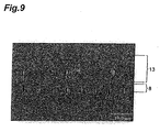
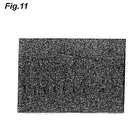
- Fig. 9 and Fig. 10 are photographs of the cross section of the silicon wafer which is cut according to the laser beam machining method described above.
- the photographs of Fig. 9 and Fig. 10 show the same cross section of the silicon wafer in different scales.
- the detailed condition when the cross section shown in Fig. 9 and Fig. 11 is formed is as follows.
- the width in the thickness direction of the silicon wafer is equal to about 13 ⁇ m
- the width of the laser moving direction is equal to about 3 ⁇ m
- the width in the thickness direction of the silicon wafer is equal to about 7 ⁇ m
- the width in the laser moving direction is equal to about 1.3 ⁇ m.
- the interval between the molten processed area 13 and the minute cavity 8 is equal to about 1.2 ⁇ m.
- Fig.11 is a photograph of a whole section shown in Fig. 9 and Fig. 10 .
- the Raman analysis is carried out on a measurement position 1 in the vicinity of the molten processed area 13, a measurement position 2 in the vicinity of the minute cavity 8, a measurement position 3 between the molten processed area 13 and the minute cavity 8, and a measurement position 4 at the upper side of the molten processed area 13.
- the spectra at the measurement positions 2, 3 and 4 had the same degree of half maximum full-width. Furthermore, as compared with reference Si (110), they had the same degree as the reference Si. Therefore, it is considered that monocrystal Si having high crystallinity might exist at all of the measurement positions 2, 3 and 4. On the other hand, a broad Raman ray was observed at the measurement position 1, and thus it is considered that polycrystal Si might exist at the measurement position 1.
- the preferable pulse pitch is around 4.00 ⁇ m. It is preferable that the machining depth (the depth in which the minute cavity is formed) is large. It is preferable that the pulse pitch is not very much increased. Estimating these totally, the pulse pitch is preferably set to 1.00 ⁇ m to 7.00 ⁇ m, and more preferably 3.00 ⁇ m to 5.00 ⁇ m. Furthermore, the machining depth (the depth in which the minute cavity is formed) is preferably set to 45 ⁇ m to 90 ⁇ m in wafer of 100 ⁇ m, and more preferably to 65 ⁇ m to 85 ⁇ m.
- the silicon wafer has a large thickness of 300 ⁇ m, it is preferable to repetitively carry out the laser beam machining process described above while varying the machining depth, and a combination of a molten processed area and a minute cavity is formed at at least one stage.
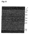
- Fig. 13 and Fig. 14 are photographs of the cross section of the thick silicon wafer which is cut according to the laser beam machining method described above.
- the photograph of Fig. 13 is the thick silicon wafer 2 which is machined from the surface 21 to the surface 22.
- the modified areas 201 to 206 are formed.
- a minute cavity is not visible; because of doing laser beam machining method multiply.
- the modified area 201, 202, 203, 204 the minute cavities are visible.
- Forming the minute cavities stress distribution is occurring around the molten processed area and the minute cavities, so that it is easy to cut.
- the minute cavities are to starting point for cutting, when add power from outside. Then, it is necessary for cutting and separating the semiconductor substrate as expand a tape that fixed it, that a condition for easily cut. Forming the minute cavities is the condition. It is especially effective for cutting semiconductor substrate that forming the molten processed area and the minute cavities.
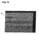
- the photograph of Fig. 14 is the thick silicon wafer 2a which is machined same method of Fig13 .
- the rough sketch of Fig. 14 is shown in Fig. 15 .
- a modified area 211 and 212 are formed in the thick silicon wafer 2a.
- the modified area 211 has a melting treated area 211 a, and a minute cavity 211b.
- the modified area 212 has a melting treated area 212a, and a minute cavity 212b.
- the minute cavities 212b are formed equally.
- the minute cavities 212b are not formed equally, so that there is an area 211c in which a minute cavity is not formed. A region where a minute cavity is difficult to forming is generate under condition of the surface.
- a melting treated area 211a is formed along the planned cutting line continuously; on the other hand a minute cavity 212b is formed here and there. Even in this case, it is easy for cutting that existence of the minute cavity. Starting points of cutting is formed along the planned cutting line, because of forming a melting treated area 211 a almost continuously. Even if the minute cavity is not exist all along the planned cutting line, exist minute cavity 212b act for fracture growing.
- a treated region which includes a treated area in the machining target along a planned cutting line of the machining target and form a minute cavity region (a second zone) which includes a minute cavity along at least one part of the planned cutting line, they are working for the starting point, so that easy to cut the machining target.
- a semiconductor substrate that is good cleavage character (e.g. GaAs)
- the modified area is preferably formed along one part of the planned cutting line. It is also prefer to form the modified area only a part which improving cutting precision.
- a laser beam is preferably made incident from a surface opposite to the pattern-formed surface.
- the broken section of the minute cavity side is apt to be smoother than the broken section of the molten processed area, and thus the yield of good products can be greatly enhanced when the minute cavities are formed at the pattern-formed surface.
- the minute cavity 182 is formed on the side of the surface, so that dividing precision of the functional element 181 side is improved. Accordingly, it is able to improve a rate of quality item, and to improve production efficiency.
- the Gaussian distribution is spread with respect to the lens aperture to use a lens incident beam like a top hat (it is preferable to increase energy of a light beam having large NA).
- NA is preferably set in the range from 0.5 to 1.0.
- the pulse width is preferably set to 500nsec or less. More preferably, it is set in the range from 10nsec to 500nsec. More preferably, it is set in the range from 10nsec to 300nsec. Further more preferably, it is set in the range from 100nsec to 200nsec.
- the molten processed area and the minute cavity are paired and also the depth of each of them has a predetermined relation with the thickness of the silicon wafer.
- the molten processed area and the minute cavity have a predetermined relation with each other in accordance with NA.
- the cutting direction is preferably parallel to or vertical to the orientation flat (ori-fla). It is preferable to form molten processed areas along the crystal orientation.
- a semiconductor wafer made from silicon is used for the machining target; raw material is not necessarily silicon.
- raw material is selected from compound semiconductor including IV group element compound except silicon or IV group element like as SiC, compound semiconductor including III-V group elements, compound semiconductor including II-VI group elements, and compound semiconductor doped various impurities.
- Pulse laser light L is irradiated to the planned cutting line 5 under a condition where multiphoton absorption can be induced and while the focus point F is positioned at the inside of the machining target 1.
- the focus point F is moved at a predetermined pitch P along the planned cutting line 5 by moving the X-axis stage 109 and the Y-axis stage 111, whereby treated areas are formed along the planned cutting line 5 in the machining target 1, and also minute cavities are formed. Accordingly, the machining target 1 can be cut off without generating any unnecessary cracks out of the planned cutting line 5 in the surface 3 of the machining target 1.
- pulse laser light L is irradiated to the planned cutting line 5 under a condition where multiphoton absorption is induced in the machining target 1 and while the focus point F is positioned at the inside of the machining target 1. Accordingly, the pulse laser light L is transmitted through the machining target 1, and the pulse laser light L is hardly absorbed at the surface 3 of the machining target 1, so that the surface 3 suffers no damage such as melting or the like due to formation of modified areas.
- the machining target 1 can be cut off without generating neither occurrence of unnecessary cracks out of the planned cutting line 5 nor melting on the surface of the machining target 1. Accordingly, as the machining target 1 is a semiconductor wafer, semiconductor chips can be taken out from the semiconductor wafer while neither unnecessary cracks out of the planned cutting line nor melting occurs. The same is satisfied in the case of a machining target on which an electrode pattern is formed, and a machining target on which an electrical device is formed, such as a piezoelectric element wafer or a glass substrate on which a display device such as liquid crystal or the like is formed. Accordingly, the yield of semiconductor chip manufactured by cutting a machining target can be enhanced.
- the width of the planned cutting line 5 (for a semiconductor wafer, this width corresponds to the interval between areas serving as semiconductor chips) can be reduced. Accordingly, the number of products which can be manufactured from one machining target 1 is increased, and thus the productivity of products can be enhanced.
- Laser light is used for cutting work of a machining target 1, and thus more complicated machining can be performed than dicing using a diamond cutter.
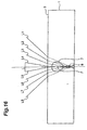
- Fig. 16 is a diagram showing this hypothesis.
- laser light L is converged to a focusing point in a machining target 1 and irradiated to the machining target 1, a treated area 7 is formed in the vicinity of the focus point F.
- light at the center portion of laser light (light corresponding to L4 and L5 in Fig. 16 ) irradiated from a laser source is used as the laser light L. This is because the center portion of the Gaussian distribution of the laser light is used.
- the inventors of this application expand laser light in order to suppress an effect of the laser light on the surface of the machining target. This is implemented by expanding laser light irradiated from a laser source through a predetermined optical system to expand the skirts of the Gaussian distribution and relatively increase the laser intensity of light (corresponding to L1 to L3 and L6 to L8 in Fig. 16 ) at the peripheral portion of the laser light.
- a treated area 7 is formed in the vicinity of the focus point F as described above, and a minute cavity 8 is formed at the portion corresponding to the treated area 7. That is, the treated area 7 and the minute cavity 8 are formed to be located along the optical axis of the laser light (indicated by a chain line in Fig. 16 ).
- the position at which the minute cavity 8 is formed corresponds to a portion on which the light of the peripheral portion of the laser light (i.e., the light corresponding to L1 to L3 and L6 to L8) is theoretically focused.
- a portion on which light at the center portion of the laser light (light at the portions corresponding to L4 and L5 in Fig. 16 ) is converged and a portion on which light at the peripheral portion of the laser light (light at the portions corresponding to L1 to L3 and L6 to L8 in Fig. 16 ) is converged are different in the thickness direction of the machining target 1 because of spherical aberration of a lens for converging the laser light.
- One hypothesis assumed by the inventors resides in that the difference in focus position as described above has some effect.
- the hypothesis supported by the inventors is as follows.
- the focus portion for light at the peripheral portion of the laser light (corresponding to L1 to L3 and L6 to L8 in Fig. 16 ) is theoretically a laser focusing point, so that it is estimated that the intensity of the light at this portion is high. Accordingly, micro-structural variation occurs at the portion due to the high-intensity light, however, substantially no crystal structural variation occurs at the peripheral portion of this focus portion. Therefore, a minute cavity 8 is formed at the peripheral portion. On the other hand, a great thermal effect is applied at the portion where the treated area 7 is formed, and thus this portion is merely melted and then re-solidified.
- Fig. 17 is a diagram showing the above hypothesis.
- laser light having a Gaussian distribution 81 When laser light having a Gaussian distribution 81 is emitted, it is transmitted through an optical system 82 and then irradiated to a machining target 83.
- a machining target 83 As shown in Fig. 8 , light at the peripheral portion of the laser light (indicated by broken lines of Fig. 17 ) is converged in the vicinity of a portion where a minute cavity 832 is formed.
- light at a relatively high-intensity portion of the laser light in the Gaussian distribution 81 is converged in the vicinity of a portion where a treated area 831 is formed.
Claims (2)
- Puce semi-conductrice extraite d'une tranche de semi-conducteur (1), dans laquelle le substrat semi-conducteur présente une structure monocristalline de silicium, dans laquelle la puce semi-conductrice présente une surface découpée formée en provoquant une fracture lorsque la tranche de semi-conducteur est découpée,
caractérisée en ce que la surface découpée comprend au moins une région traitée fondue (7) et au moins une cavité minuscule (8) formée par un faisceau laser selon une direction de l'épaisseur de la puce semi-conductrice dans une partie de la surface découpée,
dans laquelle ladite au moins une région traitée fondue (7) comprend une pluralité de régions traitées fondues formées selon une direction perpendiculaire à la direction de l'épaisseur, et ladite au moins une cavité minuscule (8) comprend une pluralité de cavités minuscules formées selon la direction perpendiculaire à la direction de l'épaisseur, dans laquelle les cavités minuscules (8) sont toutes espacées d'un intervalle prédéterminé le long de la surface de découpage,
dans laquelle la région traitée fondue (7) et la cavité minuscule (8) sont espacées entre elles d'un intervalle prédéterminé,
dans laquelle la région traitée fondue (7) présente une structure polycristalline de silicium et la cavité minuscule (8) présente une structure monocristalline de silicium. - Puce semi-conductrice selon la revendication 1, dans laquelle la puce semi-conductrice présente une surface formée avec un élément fonctionnel, et la cavité minuscule (8) est formée entre la surface et les régions traitées fondues.
Applications Claiming Priority (2)
| Application Number | Priority Date | Filing Date | Title |
|---|---|---|---|
| JP2003277039 | 2003-07-18 | ||
| EP04747689A EP1649965B1 (fr) | 2003-07-18 | 2004-07-16 | Procede d'usinage par faisceau laser d'une cible a usiner |
Related Parent Applications (3)
| Application Number | Title | Priority Date | Filing Date |
|---|---|---|---|
| EP04747689.0 Division | 2004-07-16 | ||
| EP04747689A Division-Into EP1649965B1 (fr) | 2003-07-18 | 2004-07-16 | Procede d'usinage par faisceau laser d'une cible a usiner |
| EP04747689A Division EP1649965B1 (fr) | 2003-07-18 | 2004-07-16 | Procede d'usinage par faisceau laser d'une cible a usiner |
Publications (2)
| Publication Number | Publication Date |
|---|---|
| EP2269765A1 EP2269765A1 (fr) | 2011-01-05 |
| EP2269765B1 true EP2269765B1 (fr) | 2014-10-15 |
Family
ID=34074622
Family Applications (4)
| Application Number | Title | Priority Date | Filing Date |
|---|---|---|---|
| EP11001001.4A Active EP2324950B1 (fr) | 2003-07-18 | 2004-07-16 | Substrat semiconducteur devant être coupé comprenant des zones traitées et avec des micro-cavités, et méthode de découpe d'un tel substrat |
| EP04747689A Active EP1649965B1 (fr) | 2003-07-18 | 2004-07-16 | Procede d'usinage par faisceau laser d'une cible a usiner |
| EP10009404.4A Active EP2269765B1 (fr) | 2003-07-18 | 2004-07-16 | Chip semiconducteur découpé |
| EP11001000.6A Active EP2332687B1 (fr) | 2003-07-18 | 2004-07-16 | Méthode d'usinage par faisceau laser d'une pièce à usiner utilisant un faisceau laser pulsé et une feuille d'adhésif expensif pour couper un objet à usiner |
Family Applications Before (2)
| Application Number | Title | Priority Date | Filing Date |
|---|---|---|---|
| EP11001001.4A Active EP2324950B1 (fr) | 2003-07-18 | 2004-07-16 | Substrat semiconducteur devant être coupé comprenant des zones traitées et avec des micro-cavités, et méthode de découpe d'un tel substrat |
| EP04747689A Active EP1649965B1 (fr) | 2003-07-18 | 2004-07-16 | Procede d'usinage par faisceau laser d'une cible a usiner |
Family Applications After (1)
| Application Number | Title | Priority Date | Filing Date |
|---|---|---|---|
| EP11001000.6A Active EP2332687B1 (fr) | 2003-07-18 | 2004-07-16 | Méthode d'usinage par faisceau laser d'une pièce à usiner utilisant un faisceau laser pulsé et une feuille d'adhésif expensif pour couper un objet à usiner |
Country Status (9)
| Country | Link |
|---|---|
| US (3) | US7605344B2 (fr) |
| EP (4) | EP2324950B1 (fr) |
| JP (3) | JP5122611B2 (fr) |
| KR (3) | KR101119387B1 (fr) |
| CN (3) | CN101862907B (fr) |
| ES (1) | ES2523432T3 (fr) |
| MY (1) | MY157824A (fr) |
| TW (4) | TWI406726B (fr) |
| WO (1) | WO2005007335A1 (fr) |
Families Citing this family (156)
| Publication number | Priority date | Publication date | Assignee | Title |
|---|---|---|---|---|
| JP4659300B2 (ja) | 2000-09-13 | 2011-03-30 | 浜松ホトニクス株式会社 | レーザ加工方法及び半導体チップの製造方法 |
| DE60335538D1 (de) | 2002-03-12 | 2011-02-10 | Hamamatsu Photonics Kk | Verfahren zum schneiden eines bearbeiteten objekts |
| TWI326626B (en) | 2002-03-12 | 2010-07-01 | Hamamatsu Photonics Kk | Laser processing method |
| ES2377521T3 (es) | 2002-03-12 | 2012-03-28 | Hamamatsu Photonics K.K. | Método para dividir un sustrato |
| TWI520269B (zh) | 2002-12-03 | 2016-02-01 | Hamamatsu Photonics Kk | Cutting method of semiconductor substrate |
| FR2852250B1 (fr) | 2003-03-11 | 2009-07-24 | Jean Luc Jouvin | Fourreau de protection pour canule, un ensemble d'injection comportant un tel fourreau et aiguille equipee d'un tel fourreau |
| EP1609559B1 (fr) | 2003-03-12 | 2007-08-08 | Hamamatsu Photonics K. K. | Methode d'usinage par faisceau laser |
| KR101119387B1 (ko) * | 2003-07-18 | 2012-03-07 | 하마마츠 포토닉스 가부시키가이샤 | 절단방법 |
| JP4563097B2 (ja) | 2003-09-10 | 2010-10-13 | 浜松ホトニクス株式会社 | 半導体基板の切断方法 |
| JP4509578B2 (ja) * | 2004-01-09 | 2010-07-21 | 浜松ホトニクス株式会社 | レーザ加工方法及びレーザ加工装置 |
| JP4598407B2 (ja) * | 2004-01-09 | 2010-12-15 | 浜松ホトニクス株式会社 | レーザ加工方法及びレーザ加工装置 |
| JP4601965B2 (ja) * | 2004-01-09 | 2010-12-22 | 浜松ホトニクス株式会社 | レーザ加工方法及びレーザ加工装置 |
| EP1742253B1 (fr) | 2004-03-30 | 2012-05-09 | Hamamatsu Photonics K.K. | Procede de traitement au laser |
| CN101434010B (zh) * | 2004-08-06 | 2011-04-13 | 浜松光子学株式会社 | 激光加工方法及半导体装置 |
| JP4917257B2 (ja) * | 2004-11-12 | 2012-04-18 | 浜松ホトニクス株式会社 | レーザ加工方法 |
| JP2006315017A (ja) * | 2005-05-11 | 2006-11-24 | Canon Inc | レーザ切断方法および被切断部材 |
| JP4749799B2 (ja) * | 2005-08-12 | 2011-08-17 | 浜松ホトニクス株式会社 | レーザ加工方法 |
| US9138913B2 (en) | 2005-09-08 | 2015-09-22 | Imra America, Inc. | Transparent material processing with an ultrashort pulse laser |
| DE102006042280A1 (de) * | 2005-09-08 | 2007-06-06 | IMRA America, Inc., Ann Arbor | Bearbeitung von transparentem Material mit einem Ultrakurzpuls-Laser |
| JP4762653B2 (ja) * | 2005-09-16 | 2011-08-31 | 浜松ホトニクス株式会社 | レーザ加工方法及びレーザ加工装置 |
| WO2007055010A1 (fr) * | 2005-11-10 | 2007-05-18 | Renesas Technology Corp. | Procede de fabrication d'un dispositif semi-conducteur et dispositif semi-conducteur |
| JP2007165850A (ja) | 2005-11-16 | 2007-06-28 | Denso Corp | ウェハおよびウェハの分断方法 |
| JP4907965B2 (ja) * | 2005-11-25 | 2012-04-04 | 浜松ホトニクス株式会社 | レーザ加工方法 |
| JP4804911B2 (ja) * | 2005-12-22 | 2011-11-02 | 浜松ホトニクス株式会社 | レーザ加工装置 |
| JP4907984B2 (ja) * | 2005-12-27 | 2012-04-04 | 浜松ホトニクス株式会社 | レーザ加工方法及び半導体チップ |
| US20070298529A1 (en) * | 2006-05-31 | 2007-12-27 | Toyoda Gosei, Co., Ltd. | Semiconductor light-emitting device and method for separating semiconductor light-emitting devices |
| JP5183892B2 (ja) | 2006-07-03 | 2013-04-17 | 浜松ホトニクス株式会社 | レーザ加工方法 |
| ES2428826T3 (es) | 2006-07-03 | 2013-11-11 | Hamamatsu Photonics K.K. | Procedimiento de procesamiento por láser y chip |
| JP4954653B2 (ja) * | 2006-09-19 | 2012-06-20 | 浜松ホトニクス株式会社 | レーザ加工方法 |
| EP2065120B1 (fr) | 2006-09-19 | 2015-07-01 | Hamamatsu Photonics K.K. | Procédé de traitement au laser |
| JP5101073B2 (ja) * | 2006-10-02 | 2012-12-19 | 浜松ホトニクス株式会社 | レーザ加工装置 |
| JP4964554B2 (ja) * | 2006-10-03 | 2012-07-04 | 浜松ホトニクス株式会社 | レーザ加工方法 |
| JP5132911B2 (ja) * | 2006-10-03 | 2013-01-30 | 浜松ホトニクス株式会社 | レーザ加工方法 |
| CN101522362B (zh) * | 2006-10-04 | 2012-11-14 | 浜松光子学株式会社 | 激光加工方法 |
| US8486742B2 (en) * | 2006-11-21 | 2013-07-16 | Epistar Corporation | Method for manufacturing high efficiency light-emitting diodes |
| JP5336054B2 (ja) * | 2007-07-18 | 2013-11-06 | 浜松ホトニクス株式会社 | 加工情報供給装置を備える加工情報供給システム |
| JP5449665B2 (ja) | 2007-10-30 | 2014-03-19 | 浜松ホトニクス株式会社 | レーザ加工方法 |
| JP5134928B2 (ja) * | 2007-11-30 | 2013-01-30 | 浜松ホトニクス株式会社 | 加工対象物研削方法 |
| JP5054496B2 (ja) * | 2007-11-30 | 2012-10-24 | 浜松ホトニクス株式会社 | 加工対象物切断方法 |
| US8900715B2 (en) * | 2008-06-11 | 2014-12-02 | Infineon Technologies Ag | Semiconductor device |
| JP5692969B2 (ja) | 2008-09-01 | 2015-04-01 | 浜松ホトニクス株式会社 | 収差補正方法、この収差補正方法を用いたレーザ加工方法、この収差補正方法を用いたレーザ照射方法、収差補正装置、及び、収差補正プログラム |
| WO2010048733A1 (fr) * | 2008-10-29 | 2010-05-06 | Oerlikon Solar Ip Ag, Trübbach | Procédé permettant de diviser une couche semi-conductrice formée sur un substrat en plusieurs régions au moyen de multiples irradiations par faisceau laser |
| JP5254761B2 (ja) | 2008-11-28 | 2013-08-07 | 浜松ホトニクス株式会社 | レーザ加工装置 |
| JP5241525B2 (ja) | 2009-01-09 | 2013-07-17 | 浜松ホトニクス株式会社 | レーザ加工装置 |
| JP5241527B2 (ja) | 2009-01-09 | 2013-07-17 | 浜松ホトニクス株式会社 | レーザ加工装置 |
| EP2394775B1 (fr) | 2009-02-09 | 2019-04-03 | Hamamatsu Photonics K.K. | Procédé de découpe d'une pièce |
| US8347651B2 (en) * | 2009-02-19 | 2013-01-08 | Corning Incorporated | Method of separating strengthened glass |
| US9035216B2 (en) | 2009-04-07 | 2015-05-19 | Hamamatsu Photonics K.K. | Method and device for controlling interior fractures by controlling the laser pulse width |
| JP5491761B2 (ja) | 2009-04-20 | 2014-05-14 | 浜松ホトニクス株式会社 | レーザ加工装置 |
| JP5476063B2 (ja) * | 2009-07-28 | 2014-04-23 | 浜松ホトニクス株式会社 | 加工対象物切断方法 |
| KR20120073249A (ko) * | 2009-08-28 | 2012-07-04 | 코닝 인코포레이티드 | 화학적으로 강화된 유리 기판으로부터 제품을 레이저 절단하기 위한 방법 |
| JP5446631B2 (ja) * | 2009-09-10 | 2014-03-19 | アイシン精機株式会社 | レーザ加工方法及びレーザ加工装置 |
| JP5410250B2 (ja) | 2009-11-25 | 2014-02-05 | 浜松ホトニクス株式会社 | レーザ加工方法及びレーザ加工装置 |
| US20110127242A1 (en) * | 2009-11-30 | 2011-06-02 | Xinghua Li | Methods for laser scribing and separating glass substrates |
| US8946590B2 (en) | 2009-11-30 | 2015-02-03 | Corning Incorporated | Methods for laser scribing and separating glass substrates |
| US20120234807A1 (en) * | 2009-12-07 | 2012-09-20 | J.P. Sercel Associates Inc. | Laser scribing with extended depth affectation into a workplace |
| US20130256286A1 (en) * | 2009-12-07 | 2013-10-03 | Ipg Microsystems Llc | Laser processing using an astigmatic elongated beam spot and using ultrashort pulses and/or longer wavelengths |
| US20110132885A1 (en) * | 2009-12-07 | 2011-06-09 | J.P. Sercel Associates, Inc. | Laser machining and scribing systems and methods |
| JP2011201759A (ja) * | 2010-03-05 | 2011-10-13 | Namiki Precision Jewel Co Ltd | 多層膜付き単結晶基板、多層膜付き単結晶基板の製造方法および素子製造方法 |
| JP5770436B2 (ja) * | 2010-07-08 | 2015-08-26 | 株式会社ディスコ | レーザー加工装置およびレーザー加工方法 |
| CN103079747B (zh) | 2010-07-12 | 2016-08-03 | 罗芬-西纳技术有限公司 | 由激光成丝作用进行材料处理的方法 |
| KR101940332B1 (ko) * | 2010-07-26 | 2019-01-18 | 하마마츠 포토닉스 가부시키가이샤 | 기판 가공 방법 |
| US8722516B2 (en) | 2010-09-28 | 2014-05-13 | Hamamatsu Photonics K.K. | Laser processing method and method for manufacturing light-emitting device |
| US8748236B2 (en) * | 2010-11-10 | 2014-06-10 | Toyota Jidosha Kabushiki Kaisha | Method for manufacturing semiconductor device |
| JP4945835B1 (ja) * | 2010-11-16 | 2012-06-06 | 株式会社東京精密 | レーザダイシング装置及び方法、割断装置及び方法、並びに、ウェーハ処理方法 |
| JP5480169B2 (ja) | 2011-01-13 | 2014-04-23 | 浜松ホトニクス株式会社 | レーザ加工方法 |
| JP2013042119A (ja) * | 2011-07-21 | 2013-02-28 | Hamamatsu Photonics Kk | 発光素子の製造方法 |
| TWI476064B (zh) * | 2011-11-07 | 2015-03-11 | Metal Ind Res & Dev Ct | 硬脆材料切割方法 |
| US8624348B2 (en) | 2011-11-11 | 2014-01-07 | Invensas Corporation | Chips with high fracture toughness through a metal ring |
| KR101276637B1 (ko) * | 2011-12-13 | 2013-06-19 | 한국표준과학연구원 | 레이저 다중 선로 공정에서의 가공 중 평가 방법 및 장치 |
| US9828278B2 (en) | 2012-02-28 | 2017-11-28 | Electro Scientific Industries, Inc. | Method and apparatus for separation of strengthened glass and articles produced thereby |
| CN104136967B (zh) * | 2012-02-28 | 2018-02-16 | 伊雷克托科学工业股份有限公司 | 用于分离增强玻璃的方法及装置及由该增强玻璃生产的物品 |
| US10357850B2 (en) | 2012-09-24 | 2019-07-23 | Electro Scientific Industries, Inc. | Method and apparatus for machining a workpiece |
| US8652940B2 (en) | 2012-04-10 | 2014-02-18 | Applied Materials, Inc. | Wafer dicing used hybrid multi-step laser scribing process with plasma etch |
| US8842358B2 (en) | 2012-08-01 | 2014-09-23 | Gentex Corporation | Apparatus, method, and process with laser induced channel edge |
| KR20140019549A (ko) * | 2012-08-06 | 2014-02-17 | 주성엔지니어링(주) | 유기발광장치의 제조방법 |
| JP6003496B2 (ja) * | 2012-10-02 | 2016-10-05 | 三星ダイヤモンド工業株式会社 | パターン付き基板の加工方法 |
| JP6036173B2 (ja) * | 2012-10-31 | 2016-11-30 | 三星ダイヤモンド工業株式会社 | レーザー加工装置 |
| US8785234B2 (en) | 2012-10-31 | 2014-07-22 | Infineon Technologies Ag | Method for manufacturing a plurality of chips |
| WO2014079478A1 (fr) | 2012-11-20 | 2014-05-30 | Light In Light Srl | Traitement par laser à grande vitesse de matériaux transparents |
| EP2754524B1 (fr) | 2013-01-15 | 2015-11-25 | Corning Laser Technologies GmbH | Procédé et dispositif destinés au traitement basé sur laser de substrats plats, galette ou élément en verre, utilisant un faisceau laser en ligne |
| EP2781296B1 (fr) | 2013-03-21 | 2020-10-21 | Corning Laser Technologies GmbH | Dispositif et procédé de découpe de contours à partir de substrats plats au moyen d'un laser |
| US9102011B2 (en) | 2013-08-02 | 2015-08-11 | Rofin-Sinar Technologies Inc. | Method and apparatus for non-ablative, photoacoustic compression machining in transparent materials using filamentation by burst ultrafast laser pulses |
| JP6241174B2 (ja) * | 2013-09-25 | 2017-12-06 | 三星ダイヤモンド工業株式会社 | レーザー加工装置、および、パターン付き基板の加工条件設定方法 |
| US10017410B2 (en) | 2013-10-25 | 2018-07-10 | Rofin-Sinar Technologies Llc | Method of fabricating a glass magnetic hard drive disk platter using filamentation by burst ultrafast laser pulses |
| US10005152B2 (en) | 2013-11-19 | 2018-06-26 | Rofin-Sinar Technologies Llc | Method and apparatus for spiral cutting a glass tube using filamentation by burst ultrafast laser pulses |
| US9517929B2 (en) | 2013-11-19 | 2016-12-13 | Rofin-Sinar Technologies Inc. | Method of fabricating electromechanical microchips with a burst ultrafast laser pulses |
| US11053156B2 (en) | 2013-11-19 | 2021-07-06 | Rofin-Sinar Technologies Llc | Method of closed form release for brittle materials using burst ultrafast laser pulses |
| US10252507B2 (en) | 2013-11-19 | 2019-04-09 | Rofin-Sinar Technologies Llc | Method and apparatus for forward deposition of material onto a substrate using burst ultrafast laser pulse energy |
| US10144088B2 (en) | 2013-12-03 | 2018-12-04 | Rofin-Sinar Technologies Llc | Method and apparatus for laser processing of silicon by filamentation of burst ultrafast laser pulses |
| US9676167B2 (en) | 2013-12-17 | 2017-06-13 | Corning Incorporated | Laser processing of sapphire substrate and related applications |
| US9850160B2 (en) | 2013-12-17 | 2017-12-26 | Corning Incorporated | Laser cutting of display glass compositions |
| US9517963B2 (en) | 2013-12-17 | 2016-12-13 | Corning Incorporated | Method for rapid laser drilling of holes in glass and products made therefrom |
| US20150165560A1 (en) | 2013-12-17 | 2015-06-18 | Corning Incorporated | Laser processing of slots and holes |
| US10442719B2 (en) | 2013-12-17 | 2019-10-15 | Corning Incorporated | Edge chamfering methods |
| US9701563B2 (en) | 2013-12-17 | 2017-07-11 | Corning Incorporated | Laser cut composite glass article and method of cutting |
| US11556039B2 (en) | 2013-12-17 | 2023-01-17 | Corning Incorporated | Electrochromic coated glass articles and methods for laser processing the same |
| US9815730B2 (en) | 2013-12-17 | 2017-11-14 | Corning Incorporated | Processing 3D shaped transparent brittle substrate |
| US9938187B2 (en) | 2014-02-28 | 2018-04-10 | Rofin-Sinar Technologies Llc | Method and apparatus for material processing using multiple filamentation of burst ultrafast laser pulses |
| US11041558B2 (en) | 2014-03-14 | 2021-06-22 | ZPE Licensing Inc. | Super charger components |
| TWI730945B (zh) | 2014-07-08 | 2021-06-21 | 美商康寧公司 | 用於雷射處理材料的方法與設備 |
| EP3552753A3 (fr) | 2014-07-14 | 2019-12-11 | Corning Incorporated | Système et procédé de traitement de matériaux transparents utilisant des lignes focales de faisceau laser réglables en longueur et en diamètre |
| WO2016010991A1 (fr) | 2014-07-14 | 2016-01-21 | Corning Incorporated | Bloc interface, système et procédé pour couper un substrat transparent dans une certaine plage de longueurs d'onde au moyen dudit bloc interface |
| EP3536440A1 (fr) | 2014-07-14 | 2019-09-11 | Corning Incorporated | Article en verre avec un cheminement de defauts |
| CN208586209U (zh) | 2014-07-14 | 2019-03-08 | 康宁股份有限公司 | 一种用于在工件中形成限定轮廓的多个缺陷的系统 |
| US9757815B2 (en) | 2014-07-21 | 2017-09-12 | Rofin-Sinar Technologies Inc. | Method and apparatus for performing laser curved filamentation within transparent materials |
| JP6390898B2 (ja) * | 2014-08-22 | 2018-09-19 | アイシン精機株式会社 | 基板の製造方法、加工対象物の切断方法、及び、レーザ加工装置 |
| US10017411B2 (en) | 2014-11-19 | 2018-07-10 | Corning Incorporated | Methods of separating a glass web |
| US9873628B1 (en) | 2014-12-02 | 2018-01-23 | Coherent Kaiserslautern GmbH | Filamentary cutting of brittle materials using a picosecond pulsed laser |
| US10047001B2 (en) | 2014-12-04 | 2018-08-14 | Corning Incorporated | Glass cutting systems and methods using non-diffracting laser beams |
| JP2018507154A (ja) | 2015-01-12 | 2018-03-15 | コーニング インコーポレイテッド | マルチフォトン吸収方法を用いた熱強化基板のレーザー切断 |
| US10391588B2 (en) | 2015-01-13 | 2019-08-27 | Rofin-Sinar Technologies Llc | Method and system for scribing brittle material followed by chemical etching |
| JP7292006B2 (ja) | 2015-03-24 | 2023-06-16 | コーニング インコーポレイテッド | ディスプレイガラス組成物のレーザ切断及び加工 |
| CN107666983B (zh) | 2015-03-27 | 2020-10-02 | 康宁股份有限公司 | 可透气窗及其制造方法 |
| EP3319911B1 (fr) | 2015-07-10 | 2023-04-19 | Corning Incorporated | Procédés de fabrication en continu de trous dans des feuilles de substrat flexible et produits associés |
| JP2017081804A (ja) * | 2015-10-30 | 2017-05-18 | 日本電気硝子株式会社 | 管ガラスの切断方法及び切断装置、並びに管ガラス製品の製造方法 |
| US10518358B1 (en) | 2016-01-28 | 2019-12-31 | AdlOptica Optical Systems GmbH | Multi-focus optics |
| JP2017152569A (ja) * | 2016-02-25 | 2017-08-31 | 株式会社ディスコ | ウエーハの加工方法 |
| SG11201809797PA (en) | 2016-05-06 | 2018-12-28 | Corning Inc | Laser cutting and removal of contoured shapes from transparent substrates |
| CN107398644A (zh) * | 2016-05-18 | 2017-11-28 | 南京魔迪多维数码科技有限公司 | 一种切割脆性材料的方法 |
| CN107398640A (zh) * | 2016-05-18 | 2017-11-28 | 南京魔迪多维数码科技有限公司 | 一种切割脆性材料的方法及系统 |
| US10410883B2 (en) | 2016-06-01 | 2019-09-10 | Corning Incorporated | Articles and methods of forming vias in substrates |
| US10794679B2 (en) | 2016-06-29 | 2020-10-06 | Corning Incorporated | Method and system for measuring geometric parameters of through holes |
| US20180015569A1 (en) * | 2016-07-18 | 2018-01-18 | Nanya Technology Corporation | Chip and method of manufacturing chips |
| KR20190035805A (ko) | 2016-07-29 | 2019-04-03 | 코닝 인코포레이티드 | 레이저 처리를 위한 장치 및 방법 |
| CN110121398B (zh) | 2016-08-30 | 2022-02-08 | 康宁股份有限公司 | 透明材料的激光加工 |
| KR102566170B1 (ko) * | 2016-09-12 | 2023-08-10 | 삼성전자주식회사 | 웨이퍼 타공 장치 |
| KR102078294B1 (ko) | 2016-09-30 | 2020-02-17 | 코닝 인코포레이티드 | 비-축대칭 빔 스폿을 이용하여 투명 워크피스를 레이저 가공하기 위한 기기 및 방법 |
| US11542190B2 (en) | 2016-10-24 | 2023-01-03 | Corning Incorporated | Substrate processing station for laser-based machining of sheet-like glass substrates |
| US10752534B2 (en) | 2016-11-01 | 2020-08-25 | Corning Incorporated | Apparatuses and methods for laser processing laminate workpiece stacks |
| US10668561B2 (en) | 2016-11-15 | 2020-06-02 | Coherent, Inc. | Laser apparatus for cutting brittle material |
| WO2018126078A1 (fr) | 2016-12-30 | 2018-07-05 | Electro Scientific Industries, Inc. | Procédé et système permettant de prolonger la durée de vie d'une optique dans un appareil de traitement au laser |
| US10688599B2 (en) | 2017-02-09 | 2020-06-23 | Corning Incorporated | Apparatus and methods for laser processing transparent workpieces using phase shifted focal lines |
| KR102479589B1 (ko) | 2017-03-22 | 2022-12-20 | 코닝 인코포레이티드 | 유리 웹의 분리 방법들 |
| US10794663B2 (en) | 2017-05-11 | 2020-10-06 | ZPE Licensing Inc. | Laser induced friction surface on firearm |
| US10580725B2 (en) | 2017-05-25 | 2020-03-03 | Corning Incorporated | Articles having vias with geometry attributes and methods for fabricating the same |
| US11078112B2 (en) | 2017-05-25 | 2021-08-03 | Corning Incorporated | Silica-containing substrates with vias having an axially variable sidewall taper and methods for forming the same |
| US10626040B2 (en) | 2017-06-15 | 2020-04-21 | Corning Incorporated | Articles capable of individual singulation |
| JP6903532B2 (ja) * | 2017-09-20 | 2021-07-14 | キオクシア株式会社 | 半導体装置およびその製造方法 |
| US11554984B2 (en) | 2018-02-22 | 2023-01-17 | Corning Incorporated | Alkali-free borosilicate glasses with low post-HF etch roughness |
| JP7184455B2 (ja) * | 2018-06-27 | 2022-12-06 | 株式会社ディスコ | ウェーハの加工方法 |
| US11075496B2 (en) | 2018-06-28 | 2021-07-27 | Samsung Electronics Co., Ltd. | Laser dicing device, method of laser beam modulation, and method of dicing a substrate |
| JP7118804B2 (ja) * | 2018-08-17 | 2022-08-16 | キオクシア株式会社 | 半導体装置の製造方法 |
| US10589445B1 (en) * | 2018-10-29 | 2020-03-17 | Semivation, LLC | Method of cleaving a single crystal substrate parallel to its active planar surface and method of using the cleaved daughter substrate |
| WO2020130165A1 (fr) * | 2018-12-18 | 2020-06-25 | 이석준 | Procédé de traitement de découpe au laser pour matériaux fragiles |
| US10562130B1 (en) | 2018-12-29 | 2020-02-18 | Cree, Inc. | Laser-assisted method for parting crystalline material |
| US11024501B2 (en) | 2018-12-29 | 2021-06-01 | Cree, Inc. | Carrier-assisted method for parting crystalline material along laser damage region |
| US10576585B1 (en) | 2018-12-29 | 2020-03-03 | Cree, Inc. | Laser-assisted method for parting crystalline material |
| KR20200111421A (ko) | 2019-03-19 | 2020-09-29 | 삼성전자주식회사 | 레이저 장치 및 이를 이용한 기판 다이싱 장치 및 방법 |
| US10611052B1 (en) | 2019-05-17 | 2020-04-07 | Cree, Inc. | Silicon carbide wafers with relaxed positive bow and related methods |
| JP7326053B2 (ja) * | 2019-07-11 | 2023-08-15 | 株式会社ディスコ | 被加工物の加工方法 |
| KR102216294B1 (ko) | 2020-07-22 | 2021-02-18 | 주식회사 아이티아이 | 세라믹 절단법 및 장비 |
| KR102216298B1 (ko) | 2020-04-28 | 2021-02-18 | 주식회사 아이티아이 | 세라믹 절단법 및 장비 |
| WO2021221378A1 (fr) | 2020-04-28 | 2021-11-04 | 주식회사 아이티아이 | Procédé et équipement de coupe de céramique |
| KR102241518B1 (ko) | 2020-11-17 | 2021-04-19 | 주식회사 아이티아이 | 세라믹 절단방법 및 장치 |
| CN113618261B (zh) * | 2021-10-11 | 2022-01-07 | 武汉锐科光纤激光技术股份有限公司 | 一种激光切割玻璃的切割方法 |
Family Cites Families (108)
| Publication number | Priority date | Publication date | Assignee | Title |
|---|---|---|---|---|
| US1000000A (en) * | 1910-04-25 | 1911-08-08 | Francis H Holton | Vehicle-tire. |
| JPS4624989Y1 (fr) | 1967-08-31 | 1971-08-28 | ||
| US3629545A (en) | 1967-12-19 | 1971-12-21 | Western Electric Co | Laser substrate parting |
| JPH0611071B2 (ja) | 1983-09-07 | 1994-02-09 | 三洋電機株式会社 | 化合物半導体基板の分割方法 |
| US4546231A (en) * | 1983-11-14 | 1985-10-08 | Group Ii Manufacturing Ltd. | Creation of a parting zone in a crystal structure |
| US4562333A (en) | 1984-09-04 | 1985-12-31 | General Electric Company | Stress assisted cutting of high temperature embrittled materials |
| JPS61112345A (ja) | 1984-11-07 | 1986-05-30 | Toshiba Corp | 半導体装置の製造方法 |
| JP2891264B2 (ja) | 1990-02-09 | 1999-05-17 | ローム 株式会社 | 半導体装置の製造方法 |
| JP3024990B2 (ja) * | 1990-08-31 | 2000-03-27 | 日本石英硝子株式会社 | 石英ガラス材料の切断加工方法 |
| US5211805A (en) | 1990-12-19 | 1993-05-18 | Rangaswamy Srinivasan | Cutting of organic solids by continuous wave ultraviolet irradiation |
| JPH0639572A (ja) | 1991-01-11 | 1994-02-15 | Souei Tsusho Kk | ウェハ割断装置 |
| JP3165192B2 (ja) | 1991-03-28 | 2001-05-14 | 株式会社東芝 | 半導体集積回路装置の製造方法 |
| DK0564093T3 (da) | 1992-04-01 | 2000-03-27 | Pfizer | Hydroxylerede metabolitter og derivater af doxazosin som antiatherosklerosemidler |
| US5637244A (en) | 1993-05-13 | 1997-06-10 | Podarok International, Inc. | Method and apparatus for creating an image by a pulsed laser beam inside a transparent material |
| JP2616247B2 (ja) | 1993-07-24 | 1997-06-04 | 日本電気株式会社 | 半導体装置の製造方法 |
| JPH0740336A (ja) | 1993-07-30 | 1995-02-10 | Sumitomo Electric Ind Ltd | ダイヤモンドの加工方法 |
| JP3162255B2 (ja) * | 1994-02-24 | 2001-04-25 | 三菱電機株式会社 | レーザ加工方法及びその装置 |
| US5776220A (en) | 1994-09-19 | 1998-07-07 | Corning Incorporated | Method and apparatus for breaking brittle materials |
| US5622540A (en) | 1994-09-19 | 1997-04-22 | Corning Incorporated | Method for breaking a glass sheet |
| US5543365A (en) | 1994-12-02 | 1996-08-06 | Texas Instruments Incorporated | Wafer scribe technique using laser by forming polysilicon |
| EP0847317B1 (fr) | 1995-08-31 | 2003-08-27 | Corning Incorporated | Procede et appareil servant a briser des materiaux cassants |
| KR0171947B1 (ko) | 1995-12-08 | 1999-03-20 | 김주용 | 반도체소자 제조를 위한 노광 방법 및 그를 이용한 노광장치 |
| JPH10163780A (ja) | 1996-12-04 | 1998-06-19 | Ngk Insulators Ltd | 圧電単結晶からなる振動子の製造方法 |
| JPH10305420A (ja) | 1997-03-04 | 1998-11-17 | Ngk Insulators Ltd | 酸化物単結晶からなる母材の加工方法、機能性デバイスの製造方法 |
| DE19728766C1 (de) | 1997-07-07 | 1998-12-17 | Schott Rohrglas Gmbh | Verwendung eines Verfahrens zur Herstellung einer Sollbruchstelle bei einem Glaskörper |
| JP3231708B2 (ja) * | 1997-09-26 | 2001-11-26 | 住友重機械工業株式会社 | 透明材料のマーキング方法 |
| JP3292294B2 (ja) | 1997-11-07 | 2002-06-17 | 住友重機械工業株式会社 | レーザを用いたマーキング方法及びマーキング装置 |
| JP3208730B2 (ja) * | 1998-01-16 | 2001-09-17 | 住友重機械工業株式会社 | 光透過性材料のマーキング方法 |
| JP3449201B2 (ja) | 1997-11-28 | 2003-09-22 | 日亜化学工業株式会社 | 窒化物半導体素子の製造方法 |
| JP3604550B2 (ja) | 1997-12-16 | 2004-12-22 | 日亜化学工業株式会社 | 窒化物半導体素子の製造方法 |
| JP4132172B2 (ja) | 1998-02-06 | 2008-08-13 | 浜松ホトニクス株式会社 | パルスレーザ加工装置 |
| JP2000015467A (ja) | 1998-07-01 | 2000-01-18 | Shin Meiwa Ind Co Ltd | 光による被加工材の加工方法および加工装置 |
| JP3605651B2 (ja) | 1998-09-30 | 2004-12-22 | 日立化成工業株式会社 | 半導体装置の製造方法 |
| JP3178524B2 (ja) | 1998-11-26 | 2001-06-18 | 住友重機械工業株式会社 | レーザマーキング方法と装置及びマーキングされた部材 |
| US6420678B1 (en) | 1998-12-01 | 2002-07-16 | Brian L. Hoekstra | Method for separating non-metallic substrates |
| US6259058B1 (en) | 1998-12-01 | 2001-07-10 | Accudyne Display And Semiconductor Systems, Inc. | Apparatus for separating non-metallic substrates |
| US6211488B1 (en) | 1998-12-01 | 2001-04-03 | Accudyne Display And Semiconductor Systems, Inc. | Method and apparatus for separating non-metallic substrates utilizing a laser initiated scribe |
| US6252197B1 (en) | 1998-12-01 | 2001-06-26 | Accudyne Display And Semiconductor Systems, Inc. | Method and apparatus for separating non-metallic substrates utilizing a supplemental mechanical force applicator |
| JP2000195828A (ja) | 1998-12-25 | 2000-07-14 | Denso Corp | ウエハの切断分離方法およびウエハの切断分離装置 |
| JP2000219528A (ja) | 1999-01-18 | 2000-08-08 | Samsung Sdi Co Ltd | ガラス基板の切断方法及びその装置 |
| KR100578309B1 (ko) * | 1999-08-13 | 2006-05-11 | 삼성전자주식회사 | 레이저 커팅 장치 및 이를 이용한 유리 기판 커팅 방법 |
| CN1413136A (zh) | 1999-11-24 | 2003-04-23 | 应用光子学公司 | 非金属材料的分离方法和装置 |
| JP2001250798A (ja) | 2000-03-06 | 2001-09-14 | Sony Corp | ケガキ線で材料を分割する方法及び装置 |
| AU2001261402A1 (en) | 2000-05-11 | 2001-11-20 | Ptg Precision Technology Center Limited Llc | System for cutting brittle materials |
| AU2001266919A1 (en) * | 2000-06-15 | 2001-12-24 | 3M Innovative Properties Company | Multipass multiphoton absorption method and apparatus |
| JP2002050589A (ja) | 2000-08-03 | 2002-02-15 | Sony Corp | 半導体ウェーハの延伸分離方法及び装置 |
| JP4762458B2 (ja) * | 2000-09-13 | 2011-08-31 | 浜松ホトニクス株式会社 | レーザ加工装置 |
| JP3626442B2 (ja) | 2000-09-13 | 2005-03-09 | 浜松ホトニクス株式会社 | レーザ加工方法 |
| JP3408805B2 (ja) | 2000-09-13 | 2003-05-19 | 浜松ホトニクス株式会社 | 切断起点領域形成方法及び加工対象物切断方法 |
| JP2003001458A (ja) | 2000-09-13 | 2003-01-08 | Hamamatsu Photonics Kk | レーザ加工方法 |
| JP2003001462A (ja) * | 2000-09-13 | 2003-01-08 | Hamamatsu Photonics Kk | レーザ加工装置 |
| JP2003001473A (ja) | 2000-09-13 | 2003-01-08 | Hamamatsu Photonics Kk | レーザ加工装置 |
| JP4659300B2 (ja) * | 2000-09-13 | 2011-03-30 | 浜松ホトニクス株式会社 | レーザ加工方法及び半導体チップの製造方法 |
| JP4964376B2 (ja) | 2000-09-13 | 2012-06-27 | 浜松ホトニクス株式会社 | レーザ加工装置及びレーザ加工方法 |
| JP2002158276A (ja) | 2000-11-20 | 2002-05-31 | Hitachi Chem Co Ltd | ウエハ貼着用粘着シートおよび半導体装置 |
| JP2002226796A (ja) | 2001-01-29 | 2002-08-14 | Hitachi Chem Co Ltd | ウェハ貼着用粘着シート及び半導体装置 |
| GB2394712B (en) | 2001-03-09 | 2005-10-26 | Crystal Fibre As | Fabrication of microstructured fibres |
| JP2003154517A (ja) | 2001-11-21 | 2003-05-27 | Seiko Epson Corp | 脆性材料の割断加工方法およびその装置、並びに電子部品の製造方法 |
| DE60335538D1 (de) * | 2002-03-12 | 2011-02-10 | Hamamatsu Photonics Kk | Verfahren zum schneiden eines bearbeiteten objekts |
| TWI326626B (en) * | 2002-03-12 | 2010-07-01 | Hamamatsu Photonics Kk | Laser processing method |
| ES2377521T3 (es) * | 2002-03-12 | 2012-03-28 | Hamamatsu Photonics K.K. | Método para dividir un sustrato |
| TWI520269B (zh) * | 2002-12-03 | 2016-02-01 | Hamamatsu Photonics Kk | Cutting method of semiconductor substrate |
| CN100445014C (zh) * | 2002-12-05 | 2008-12-24 | 浜松光子学株式会社 | 激光加工装置 |
| JP2004188422A (ja) * | 2002-12-06 | 2004-07-08 | Hamamatsu Photonics Kk | レーザ加工装置及びレーザ加工方法 |
| FR2852250B1 (fr) * | 2003-03-11 | 2009-07-24 | Jean Luc Jouvin | Fourreau de protection pour canule, un ensemble d'injection comportant un tel fourreau et aiguille equipee d'un tel fourreau |
| EP1609559B1 (fr) * | 2003-03-12 | 2007-08-08 | Hamamatsu Photonics K. K. | Methode d'usinage par faisceau laser |
| JP2005012203A (ja) | 2003-05-29 | 2005-01-13 | Hamamatsu Photonics Kk | レーザ加工方法 |
| JP2005028438A (ja) | 2003-07-11 | 2005-02-03 | Disco Abrasive Syst Ltd | レーザ光線を利用する加工装置 |
| KR101119387B1 (ko) | 2003-07-18 | 2012-03-07 | 하마마츠 포토닉스 가부시키가이샤 | 절단방법 |
| JP4563097B2 (ja) * | 2003-09-10 | 2010-10-13 | 浜松ホトニクス株式会社 | 半導体基板の切断方法 |
| JP2005086175A (ja) * | 2003-09-11 | 2005-03-31 | Hamamatsu Photonics Kk | 半導体薄膜の製造方法、半導体薄膜、半導体薄膜チップ、電子管、及び光検出素子 |
| CN100461561C (zh) * | 2004-01-07 | 2009-02-11 | 浜松光子学株式会社 | 半导体发光元件及其制造方法 |
| JP4601965B2 (ja) * | 2004-01-09 | 2010-12-22 | 浜松ホトニクス株式会社 | レーザ加工方法及びレーザ加工装置 |
| JP4509578B2 (ja) * | 2004-01-09 | 2010-07-21 | 浜松ホトニクス株式会社 | レーザ加工方法及びレーザ加工装置 |
| JP4598407B2 (ja) * | 2004-01-09 | 2010-12-15 | 浜松ホトニクス株式会社 | レーザ加工方法及びレーザ加工装置 |
| JP4536407B2 (ja) * | 2004-03-30 | 2010-09-01 | 浜松ホトニクス株式会社 | レーザ加工方法及び加工対象物 |
| EP1742253B1 (fr) * | 2004-03-30 | 2012-05-09 | Hamamatsu Photonics K.K. | Procede de traitement au laser |
| EP1748474B1 (fr) * | 2004-03-30 | 2015-05-06 | Hamamatsu Photonics K.K. | Procede de traitement au laser |
| JP4634089B2 (ja) * | 2004-07-30 | 2011-02-16 | 浜松ホトニクス株式会社 | レーザ加工方法 |
| CN101434010B (zh) * | 2004-08-06 | 2011-04-13 | 浜松光子学株式会社 | 激光加工方法及半导体装置 |
| JP4754801B2 (ja) * | 2004-10-13 | 2011-08-24 | 浜松ホトニクス株式会社 | レーザ加工方法 |
| JP4917257B2 (ja) * | 2004-11-12 | 2012-04-18 | 浜松ホトニクス株式会社 | レーザ加工方法 |
| JP4781661B2 (ja) * | 2004-11-12 | 2011-09-28 | 浜松ホトニクス株式会社 | レーザ加工方法 |
| JP4198123B2 (ja) * | 2005-03-22 | 2008-12-17 | 浜松ホトニクス株式会社 | レーザ加工方法 |
| JP4776994B2 (ja) * | 2005-07-04 | 2011-09-21 | 浜松ホトニクス株式会社 | 加工対象物切断方法 |
| JP4749799B2 (ja) * | 2005-08-12 | 2011-08-17 | 浜松ホトニクス株式会社 | レーザ加工方法 |
| JP4762653B2 (ja) * | 2005-09-16 | 2011-08-31 | 浜松ホトニクス株式会社 | レーザ加工方法及びレーザ加工装置 |
| JP4237745B2 (ja) * | 2005-11-18 | 2009-03-11 | 浜松ホトニクス株式会社 | レーザ加工方法 |
| JP4907965B2 (ja) * | 2005-11-25 | 2012-04-04 | 浜松ホトニクス株式会社 | レーザ加工方法 |
| JP4804911B2 (ja) * | 2005-12-22 | 2011-11-02 | 浜松ホトニクス株式会社 | レーザ加工装置 |
| JP4907984B2 (ja) * | 2005-12-27 | 2012-04-04 | 浜松ホトニクス株式会社 | レーザ加工方法及び半導体チップ |
| JP4804183B2 (ja) * | 2006-03-20 | 2011-11-02 | 株式会社デンソー | 半導体基板の分断方法およびその分断方法で作製された半導体チップ |
| ES2428826T3 (es) * | 2006-07-03 | 2013-11-11 | Hamamatsu Photonics K.K. | Procedimiento de procesamiento por láser y chip |
| JP5183892B2 (ja) * | 2006-07-03 | 2013-04-17 | 浜松ホトニクス株式会社 | レーザ加工方法 |
| EP2065120B1 (fr) * | 2006-09-19 | 2015-07-01 | Hamamatsu Photonics K.K. | Procédé de traitement au laser |
| JP4954653B2 (ja) * | 2006-09-19 | 2012-06-20 | 浜松ホトニクス株式会社 | レーザ加工方法 |
| JP5101073B2 (ja) * | 2006-10-02 | 2012-12-19 | 浜松ホトニクス株式会社 | レーザ加工装置 |
| JP5132911B2 (ja) * | 2006-10-03 | 2013-01-30 | 浜松ホトニクス株式会社 | レーザ加工方法 |
| JP4964554B2 (ja) * | 2006-10-03 | 2012-07-04 | 浜松ホトニクス株式会社 | レーザ加工方法 |
| CN101522362B (zh) * | 2006-10-04 | 2012-11-14 | 浜松光子学株式会社 | 激光加工方法 |
| JP5336054B2 (ja) * | 2007-07-18 | 2013-11-06 | 浜松ホトニクス株式会社 | 加工情報供給装置を備える加工情報供給システム |
| JP4402708B2 (ja) * | 2007-08-03 | 2010-01-20 | 浜松ホトニクス株式会社 | レーザ加工方法、レーザ加工装置及びその製造方法 |
| JP5225639B2 (ja) * | 2007-09-06 | 2013-07-03 | 浜松ホトニクス株式会社 | 半導体レーザ素子の製造方法 |
| JP5342772B2 (ja) * | 2007-10-12 | 2013-11-13 | 浜松ホトニクス株式会社 | 加工対象物切断方法 |
| JP5449665B2 (ja) * | 2007-10-30 | 2014-03-19 | 浜松ホトニクス株式会社 | レーザ加工方法 |
| JP5054496B2 (ja) * | 2007-11-30 | 2012-10-24 | 浜松ホトニクス株式会社 | 加工対象物切断方法 |
| JP5134928B2 (ja) * | 2007-11-30 | 2013-01-30 | 浜松ホトニクス株式会社 | 加工対象物研削方法 |
| JP5241525B2 (ja) * | 2009-01-09 | 2013-07-17 | 浜松ホトニクス株式会社 | レーザ加工装置 |
-
2004
- 2004-07-16 KR KR1020107019033A patent/KR101119387B1/ko active IP Right Grant
- 2004-07-16 EP EP11001001.4A patent/EP2324950B1/fr active Active
- 2004-07-16 WO PCT/JP2004/010224 patent/WO2005007335A1/fr active Application Filing
- 2004-07-16 KR KR1020067001190A patent/KR101119289B1/ko active IP Right Grant
- 2004-07-16 US US10/564,840 patent/US7605344B2/en active Active
- 2004-07-16 CN CN201010165964.3A patent/CN101862907B/zh active Active
- 2004-07-16 EP EP04747689A patent/EP1649965B1/fr active Active
- 2004-07-16 KR KR1020117011270A patent/KR101193723B1/ko active IP Right Grant
- 2004-07-16 EP EP10009404.4A patent/EP2269765B1/fr active Active
- 2004-07-16 CN CN2004800207868A patent/CN1826207B/zh not_active Withdrawn - After Issue
- 2004-07-16 ES ES10009404.4T patent/ES2523432T3/es active Active
- 2004-07-16 CN CN201010165735.1A patent/CN101862906B/zh active Active
- 2004-07-16 EP EP11001000.6A patent/EP2332687B1/fr active Active
- 2004-07-17 TW TW099130075A patent/TWI406726B/zh active
- 2004-07-17 TW TW099124142A patent/TWI376284B/zh active
- 2004-07-17 TW TW101130413A patent/TWI590902B/zh active
- 2004-07-17 TW TW093121444A patent/TWI340676B/zh active
- 2004-07-19 MY MYPI20042893A patent/MY157824A/en unknown
-
2009
- 2009-09-24 US US12/585,780 patent/US8852698B2/en active Active
-
2010
- 2010-07-26 JP JP2010167359A patent/JP5122611B2/ja active Active
- 2010-07-26 JP JP2010167355A patent/JP5015294B2/ja active Active
- 2010-09-02 US US12/923,111 patent/US20100327416A1/en not_active Abandoned
-
2012
- 2012-07-17 JP JP2012158718A patent/JP5554378B2/ja active Active
Also Published As
Similar Documents
| Publication | Publication Date | Title |
|---|---|---|
| EP2269765B1 (fr) | Chip semiconducteur découpé | |
| EP1609559B1 (fr) | Methode d'usinage par faisceau laser | |
| US9543256B2 (en) | Substrate dividing method | |
| US8247734B2 (en) | Laser beam machining method | |
| JP4703983B2 (ja) | 切断方法 | |
| EP1609558B1 (fr) | Methode d'usinage par faisceau laser |
Legal Events
| Date | Code | Title | Description |
|---|---|---|---|
| PUAI | Public reference made under article 153(3) epc to a published international application that has entered the european phase |
Free format text: ORIGINAL CODE: 0009012 |
|
| 17P | Request for examination filed |
Effective date: 20100909 |
|
| AC | Divisional application: reference to earlier application |
Ref document number: 1649965 Country of ref document: EP Kind code of ref document: P |
|
| AK | Designated contracting states |
Kind code of ref document: A1 Designated state(s): AT BE BG CH CY CZ DE DK EE ES FI FR GB GR HU IE IT LI LU MC NL PL PT RO SE SI SK TR |
|
| 17Q | First examination report despatched |
Effective date: 20111215 |
|
| GRAP | Despatch of communication of intention to grant a patent |
Free format text: ORIGINAL CODE: EPIDOSNIGR1 |
|
| INTG | Intention to grant announced |
Effective date: 20140424 |
|
| GRAS | Grant fee paid |
Free format text: ORIGINAL CODE: EPIDOSNIGR3 |
|
| GRAA | (expected) grant |
Free format text: ORIGINAL CODE: 0009210 |
|
| AC | Divisional application: reference to earlier application |
Ref document number: 1649965 Country of ref document: EP Kind code of ref document: P |
|
| AK | Designated contracting states |
Kind code of ref document: B1 Designated state(s): AT BE BG CH CY CZ DE DK EE ES FI FR GB GR HU IE IT LI LU MC NL PL PT RO SE SI SK TR |
|
| REG | Reference to a national code |
Ref country code: GB Ref legal event code: FG4D Ref country code: CH Ref legal event code: NV Representative=s name: ISLER AND PEDRAZZINI AG, CH Ref country code: CH Ref legal event code: EP |
|
| REG | Reference to a national code |
Ref country code: IE Ref legal event code: FG4D |
|
| REG | Reference to a national code |
Ref country code: AT Ref legal event code: REF Ref document number: 691409 Country of ref document: AT Kind code of ref document: T Effective date: 20141115 |
|
| REG | Reference to a national code |
Ref country code: ES Ref legal event code: FG2A Ref document number: 2523432 Country of ref document: ES Kind code of ref document: T3 Effective date: 20141125 |
|
| REG | Reference to a national code |
Ref country code: DE Ref legal event code: R096 Ref document number: 602004046019 Country of ref document: DE Effective date: 20141127 |
|
| REG | Reference to a national code |
Ref country code: NL Ref legal event code: T3 |
|
| REG | Reference to a national code |
Ref country code: AT Ref legal event code: MK05 Ref document number: 691409 Country of ref document: AT Kind code of ref document: T Effective date: 20141015 |
|
| PG25 | Lapsed in a contracting state [announced via postgrant information from national office to epo] |
Ref country code: FI Free format text: LAPSE BECAUSE OF FAILURE TO SUBMIT A TRANSLATION OF THE DESCRIPTION OR TO PAY THE FEE WITHIN THE PRESCRIBED TIME-LIMIT Effective date: 20141015 Ref country code: PT Free format text: LAPSE BECAUSE OF FAILURE TO SUBMIT A TRANSLATION OF THE DESCRIPTION OR TO PAY THE FEE WITHIN THE PRESCRIBED TIME-LIMIT Effective date: 20150216 |
|
| PG25 | Lapsed in a contracting state [announced via postgrant information from national office to epo] |
Ref country code: GR Free format text: LAPSE BECAUSE OF FAILURE TO SUBMIT A TRANSLATION OF THE DESCRIPTION OR TO PAY THE FEE WITHIN THE PRESCRIBED TIME-LIMIT Effective date: 20150116 Ref country code: PL Free format text: LAPSE BECAUSE OF FAILURE TO SUBMIT A TRANSLATION OF THE DESCRIPTION OR TO PAY THE FEE WITHIN THE PRESCRIBED TIME-LIMIT Effective date: 20141015 Ref country code: CY Free format text: LAPSE BECAUSE OF FAILURE TO SUBMIT A TRANSLATION OF THE DESCRIPTION OR TO PAY THE FEE WITHIN THE PRESCRIBED TIME-LIMIT Effective date: 20141015 Ref country code: AT Free format text: LAPSE BECAUSE OF FAILURE TO SUBMIT A TRANSLATION OF THE DESCRIPTION OR TO PAY THE FEE WITHIN THE PRESCRIBED TIME-LIMIT Effective date: 20141015 Ref country code: SE Free format text: LAPSE BECAUSE OF FAILURE TO SUBMIT A TRANSLATION OF THE DESCRIPTION OR TO PAY THE FEE WITHIN THE PRESCRIBED TIME-LIMIT Effective date: 20141015 |
|
| REG | Reference to a national code |
Ref country code: DE Ref legal event code: R097 Ref document number: 602004046019 Country of ref document: DE |
|
| PG25 | Lapsed in a contracting state [announced via postgrant information from national office to epo] |
Ref country code: RO Free format text: LAPSE BECAUSE OF FAILURE TO SUBMIT A TRANSLATION OF THE DESCRIPTION OR TO PAY THE FEE WITHIN THE PRESCRIBED TIME-LIMIT Effective date: 20141015 Ref country code: SK Free format text: LAPSE BECAUSE OF FAILURE TO SUBMIT A TRANSLATION OF THE DESCRIPTION OR TO PAY THE FEE WITHIN THE PRESCRIBED TIME-LIMIT Effective date: 20141015 Ref country code: CZ Free format text: LAPSE BECAUSE OF FAILURE TO SUBMIT A TRANSLATION OF THE DESCRIPTION OR TO PAY THE FEE WITHIN THE PRESCRIBED TIME-LIMIT Effective date: 20141015 Ref country code: DK Free format text: LAPSE BECAUSE OF FAILURE TO SUBMIT A TRANSLATION OF THE DESCRIPTION OR TO PAY THE FEE WITHIN THE PRESCRIBED TIME-LIMIT Effective date: 20141015 Ref country code: EE Free format text: LAPSE BECAUSE OF FAILURE TO SUBMIT A TRANSLATION OF THE DESCRIPTION OR TO PAY THE FEE WITHIN THE PRESCRIBED TIME-LIMIT Effective date: 20141015 |
|
| PLBE | No opposition filed within time limit |
Free format text: ORIGINAL CODE: 0009261 |
|
| STAA | Information on the status of an ep patent application or granted ep patent |
Free format text: STATUS: NO OPPOSITION FILED WITHIN TIME LIMIT |
|
| 26N | No opposition filed |
Effective date: 20150716 |
|
| PG25 | Lapsed in a contracting state [announced via postgrant information from national office to epo] |
Ref country code: SI Free format text: LAPSE BECAUSE OF FAILURE TO SUBMIT A TRANSLATION OF THE DESCRIPTION OR TO PAY THE FEE WITHIN THE PRESCRIBED TIME-LIMIT Effective date: 20141015 Ref country code: MC Free format text: LAPSE BECAUSE OF FAILURE TO SUBMIT A TRANSLATION OF THE DESCRIPTION OR TO PAY THE FEE WITHIN THE PRESCRIBED TIME-LIMIT Effective date: 20141015 |
|
| PG25 | Lapsed in a contracting state [announced via postgrant information from national office to epo] |
Ref country code: LU Free format text: LAPSE BECAUSE OF FAILURE TO SUBMIT A TRANSLATION OF THE DESCRIPTION OR TO PAY THE FEE WITHIN THE PRESCRIBED TIME-LIMIT Effective date: 20150716 |
|
| REG | Reference to a national code |
Ref country code: IE Ref legal event code: MM4A |
|
| REG | Reference to a national code |
Ref country code: FR Ref legal event code: PLFP Year of fee payment: 13 |
|
| PG25 | Lapsed in a contracting state [announced via postgrant information from national office to epo] |
Ref country code: IE Free format text: LAPSE BECAUSE OF NON-PAYMENT OF DUE FEES Effective date: 20150716 |
|
| PG25 | Lapsed in a contracting state [announced via postgrant information from national office to epo] |
Ref country code: HU Free format text: LAPSE BECAUSE OF FAILURE TO SUBMIT A TRANSLATION OF THE DESCRIPTION OR TO PAY THE FEE WITHIN THE PRESCRIBED TIME-LIMIT; INVALID AB INITIO Effective date: 20040716 Ref country code: BG Free format text: LAPSE BECAUSE OF FAILURE TO SUBMIT A TRANSLATION OF THE DESCRIPTION OR TO PAY THE FEE WITHIN THE PRESCRIBED TIME-LIMIT Effective date: 20141015 |
|
| REG | Reference to a national code |
Ref country code: FR Ref legal event code: PLFP Year of fee payment: 14 |
|
| PG25 | Lapsed in a contracting state [announced via postgrant information from national office to epo] |
Ref country code: TR Free format text: LAPSE BECAUSE OF FAILURE TO SUBMIT A TRANSLATION OF THE DESCRIPTION OR TO PAY THE FEE WITHIN THE PRESCRIBED TIME-LIMIT Effective date: 20141015 |
|
| REG | Reference to a national code |
Ref country code: FR Ref legal event code: PLFP Year of fee payment: 15 |
|
| P01 | Opt-out of the competence of the unified patent court (upc) registered |
Effective date: 20230509 |
|
| PGFP | Annual fee paid to national office [announced via postgrant information from national office to epo] |
Ref country code: NL Payment date: 20230614 Year of fee payment: 20 Ref country code: IT Payment date: 20230612 Year of fee payment: 20 Ref country code: FR Payment date: 20230620 Year of fee payment: 20 |
|
| PGFP | Annual fee paid to national office [announced via postgrant information from national office to epo] |
Ref country code: BE Payment date: 20230616 Year of fee payment: 20 |
|
| PGFP | Annual fee paid to national office [announced via postgrant information from national office to epo] |
Ref country code: GB Payment date: 20230601 Year of fee payment: 20 Ref country code: ES Payment date: 20230801 Year of fee payment: 20 Ref country code: CH Payment date: 20230801 Year of fee payment: 20 |
|
| PGFP | Annual fee paid to national office [announced via postgrant information from national office to epo] |
Ref country code: DE Payment date: 20230531 Year of fee payment: 20 |