EP2243047B1 - Facet mirror for use in a projection exposure apparatus for microlithography - Google Patents
Facet mirror for use in a projection exposure apparatus for microlithography Download PDFInfo
- Publication number
- EP2243047B1 EP2243047B1 EP09709960.0A EP09709960A EP2243047B1 EP 2243047 B1 EP2243047 B1 EP 2243047B1 EP 09709960 A EP09709960 A EP 09709960A EP 2243047 B1 EP2243047 B1 EP 2243047B1
- Authority
- EP
- European Patent Office
- Prior art keywords
- separate
- mirror
- mirrors
- illumination
- facet mirror
- Prior art date
- Legal status (The legal status is an assumption and is not a legal conclusion. Google has not performed a legal analysis and makes no representation as to the accuracy of the status listed.)
- Active
Links
- 238000001393 microlithography Methods 0.000 title claims description 6
- 238000005286 illumination Methods 0.000 claims description 167
- 230000005855 radiation Effects 0.000 claims description 67
- 238000003384 imaging method Methods 0.000 claims description 11
- 230000000694 effects Effects 0.000 claims description 9
- 238000006073 displacement reaction Methods 0.000 claims description 8
- 230000003287 optical effect Effects 0.000 claims description 8
- 210000001747 pupil Anatomy 0.000 description 77
- 230000000875 corresponding effect Effects 0.000 description 25
- 238000009826 distribution Methods 0.000 description 24
- 238000011144 upstream manufacturing Methods 0.000 description 14
- 238000000034 method Methods 0.000 description 10
- 238000013461 design Methods 0.000 description 8
- 239000007787 solid Substances 0.000 description 8
- 230000008901 benefit Effects 0.000 description 7
- 239000011248 coating agent Substances 0.000 description 7
- 238000000576 coating method Methods 0.000 description 7
- 238000003491 array Methods 0.000 description 6
- 230000005540 biological transmission Effects 0.000 description 6
- 238000001459 lithography Methods 0.000 description 5
- 230000007935 neutral effect Effects 0.000 description 5
- 230000000903 blocking effect Effects 0.000 description 4
- 230000008569 process Effects 0.000 description 4
- 229910052710 silicon Inorganic materials 0.000 description 4
- 239000010703 silicon Substances 0.000 description 4
- 238000012876 topography Methods 0.000 description 4
- VYPSYNLAJGMNEJ-UHFFFAOYSA-N Silicium dioxide Chemical compound O=[Si]=O VYPSYNLAJGMNEJ-UHFFFAOYSA-N 0.000 description 3
- 230000015572 biosynthetic process Effects 0.000 description 3
- 238000004519 manufacturing process Methods 0.000 description 3
- 238000002310 reflectometry Methods 0.000 description 3
- 238000012546 transfer Methods 0.000 description 3
- ZOKXTWBITQBERF-UHFFFAOYSA-N Molybdenum Chemical compound [Mo] ZOKXTWBITQBERF-UHFFFAOYSA-N 0.000 description 2
- PXHVJJICTQNCMI-UHFFFAOYSA-N Nickel Chemical compound [Ni] PXHVJJICTQNCMI-UHFFFAOYSA-N 0.000 description 2
- 238000005229 chemical vapour deposition Methods 0.000 description 2
- 230000002596 correlated effect Effects 0.000 description 2
- 229910003460 diamond Inorganic materials 0.000 description 2
- 239000010432 diamond Substances 0.000 description 2
- 229910052750 molybdenum Inorganic materials 0.000 description 2
- 239000011733 molybdenum Substances 0.000 description 2
- 238000009304 pastoral farming Methods 0.000 description 2
- HBMJWWWQQXIZIP-UHFFFAOYSA-N silicon carbide Chemical compound [Si+]#[C-] HBMJWWWQQXIZIP-UHFFFAOYSA-N 0.000 description 2
- 229910010271 silicon carbide Inorganic materials 0.000 description 2
- 239000000725 suspension Substances 0.000 description 2
- QNRATNLHPGXHMA-XZHTYLCXSA-N (r)-(6-ethoxyquinolin-4-yl)-[(2s,4s,5r)-5-ethyl-1-azabicyclo[2.2.2]octan-2-yl]methanol;hydrochloride Chemical compound Cl.C([C@H]([C@H](C1)CC)C2)CN1[C@@H]2[C@H](O)C1=CC=NC2=CC=C(OCC)C=C21 QNRATNLHPGXHMA-XZHTYLCXSA-N 0.000 description 1
- 229910000838 Al alloy Inorganic materials 0.000 description 1
- RYGMFSIKBFXOCR-UHFFFAOYSA-N Copper Chemical compound [Cu] RYGMFSIKBFXOCR-UHFFFAOYSA-N 0.000 description 1
- 235000010627 Phaseolus vulgaris Nutrition 0.000 description 1
- 244000046052 Phaseolus vulgaris Species 0.000 description 1
- 239000004952 Polyamide Substances 0.000 description 1
- 238000010521 absorption reaction Methods 0.000 description 1
- 230000006978 adaptation Effects 0.000 description 1
- 230000004075 alteration Effects 0.000 description 1
- PNEYBMLMFCGWSK-UHFFFAOYSA-N aluminium oxide Inorganic materials [O-2].[O-2].[O-2].[Al+3].[Al+3] PNEYBMLMFCGWSK-UHFFFAOYSA-N 0.000 description 1
- 230000009286 beneficial effect Effects 0.000 description 1
- 230000008859 change Effects 0.000 description 1
- 229910052681 coesite Inorganic materials 0.000 description 1
- 230000000295 complement effect Effects 0.000 description 1
- 238000010276 construction Methods 0.000 description 1
- 238000011109 contamination Methods 0.000 description 1
- 238000001816 cooling Methods 0.000 description 1
- 239000000110 cooling liquid Substances 0.000 description 1
- 229910052802 copper Inorganic materials 0.000 description 1
- 239000010949 copper Substances 0.000 description 1
- 238000012937 correction Methods 0.000 description 1
- 229910052593 corundum Inorganic materials 0.000 description 1
- 229910052906 cristobalite Inorganic materials 0.000 description 1
- 230000001419 dependent effect Effects 0.000 description 1
- 238000009713 electroplating Methods 0.000 description 1
- 210000000887 face Anatomy 0.000 description 1
- 230000017525 heat dissipation Effects 0.000 description 1
- 238000000265 homogenisation Methods 0.000 description 1
- 230000010354 integration Effects 0.000 description 1
- 210000003734 kidney Anatomy 0.000 description 1
- 239000000463 material Substances 0.000 description 1
- 230000007246 mechanism Effects 0.000 description 1
- 238000002156 mixing Methods 0.000 description 1
- 238000012544 monitoring process Methods 0.000 description 1
- 229910052759 nickel Inorganic materials 0.000 description 1
- 238000012856 packing Methods 0.000 description 1
- 238000000206 photolithography Methods 0.000 description 1
- 229920002647 polyamide Polymers 0.000 description 1
- 238000012545 processing Methods 0.000 description 1
- 230000009467 reduction Effects 0.000 description 1
- 239000004065 semiconductor Substances 0.000 description 1
- 239000000377 silicon dioxide Substances 0.000 description 1
- 229910052814 silicon oxide Inorganic materials 0.000 description 1
- 238000004528 spin coating Methods 0.000 description 1
- 229910052682 stishovite Inorganic materials 0.000 description 1
- 230000001360 synchronised effect Effects 0.000 description 1
- 229910052905 tridymite Inorganic materials 0.000 description 1
- 229910001845 yogo sapphire Inorganic materials 0.000 description 1
Images


Classifications
-
- G—PHYSICS
- G03—PHOTOGRAPHY; CINEMATOGRAPHY; ANALOGOUS TECHNIQUES USING WAVES OTHER THAN OPTICAL WAVES; ELECTROGRAPHY; HOLOGRAPHY
- G03F—PHOTOMECHANICAL PRODUCTION OF TEXTURED OR PATTERNED SURFACES, e.g. FOR PRINTING, FOR PROCESSING OF SEMICONDUCTOR DEVICES; MATERIALS THEREFOR; ORIGINALS THEREFOR; APPARATUS SPECIALLY ADAPTED THEREFOR
- G03F7/00—Photomechanical, e.g. photolithographic, production of textured or patterned surfaces, e.g. printing surfaces; Materials therefor, e.g. comprising photoresists; Apparatus specially adapted therefor
- G03F7/70—Microphotolithographic exposure; Apparatus therefor
- G03F7/70058—Mask illumination systems
- G03F7/702—Reflective illumination, i.e. reflective optical elements other than folding mirrors, e.g. extreme ultraviolet [EUV] illumination systems
-
- G—PHYSICS
- G02—OPTICS
- G02B—OPTICAL ELEMENTS, SYSTEMS OR APPARATUS
- G02B26/00—Optical devices or arrangements for the control of light using movable or deformable optical elements
- G02B26/06—Optical devices or arrangements for the control of light using movable or deformable optical elements for controlling the phase of light
-
- G—PHYSICS
- G02—OPTICS
- G02B—OPTICAL ELEMENTS, SYSTEMS OR APPARATUS
- G02B26/00—Optical devices or arrangements for the control of light using movable or deformable optical elements
- G02B26/08—Optical devices or arrangements for the control of light using movable or deformable optical elements for controlling the direction of light
- G02B26/0816—Optical devices or arrangements for the control of light using movable or deformable optical elements for controlling the direction of light by means of one or more reflecting elements
- G02B26/0833—Optical devices or arrangements for the control of light using movable or deformable optical elements for controlling the direction of light by means of one or more reflecting elements the reflecting element being a micromechanical device, e.g. a MEMS mirror, DMD
-
- G—PHYSICS
- G02—OPTICS
- G02B—OPTICAL ELEMENTS, SYSTEMS OR APPARATUS
- G02B27/00—Optical systems or apparatus not provided for by any of the groups G02B1/00 - G02B26/00, G02B30/00
- G02B27/09—Beam shaping, e.g. changing the cross-sectional area, not otherwise provided for
- G02B27/0927—Systems for changing the beam intensity distribution, e.g. Gaussian to top-hat
-
- G—PHYSICS
- G02—OPTICS
- G02B—OPTICAL ELEMENTS, SYSTEMS OR APPARATUS
- G02B5/00—Optical elements other than lenses
- G02B5/08—Mirrors
- G02B5/09—Multifaceted or polygonal mirrors, e.g. polygonal scanning mirrors; Fresnel mirrors
-
- G—PHYSICS
- G03—PHOTOGRAPHY; CINEMATOGRAPHY; ANALOGOUS TECHNIQUES USING WAVES OTHER THAN OPTICAL WAVES; ELECTROGRAPHY; HOLOGRAPHY
- G03F—PHOTOMECHANICAL PRODUCTION OF TEXTURED OR PATTERNED SURFACES, e.g. FOR PRINTING, FOR PROCESSING OF SEMICONDUCTOR DEVICES; MATERIALS THEREFOR; ORIGINALS THEREFOR; APPARATUS SPECIALLY ADAPTED THEREFOR
- G03F7/00—Photomechanical, e.g. photolithographic, production of textured or patterned surfaces, e.g. printing surfaces; Materials therefor, e.g. comprising photoresists; Apparatus specially adapted therefor
- G03F7/70—Microphotolithographic exposure; Apparatus therefor
- G03F7/70058—Mask illumination systems
- G03F7/70075—Homogenization of illumination intensity in the mask plane by using an integrator, e.g. fly's eye lens, facet mirror or glass rod, by using a diffusing optical element or by beam deflection
-
- G—PHYSICS
- G03—PHOTOGRAPHY; CINEMATOGRAPHY; ANALOGOUS TECHNIQUES USING WAVES OTHER THAN OPTICAL WAVES; ELECTROGRAPHY; HOLOGRAPHY
- G03F—PHOTOMECHANICAL PRODUCTION OF TEXTURED OR PATTERNED SURFACES, e.g. FOR PRINTING, FOR PROCESSING OF SEMICONDUCTOR DEVICES; MATERIALS THEREFOR; ORIGINALS THEREFOR; APPARATUS SPECIALLY ADAPTED THEREFOR
- G03F7/00—Photomechanical, e.g. photolithographic, production of textured or patterned surfaces, e.g. printing surfaces; Materials therefor, e.g. comprising photoresists; Apparatus specially adapted therefor
- G03F7/70—Microphotolithographic exposure; Apparatus therefor
- G03F7/70058—Mask illumination systems
- G03F7/70091—Illumination settings, i.e. intensity distribution in the pupil plane or angular distribution in the field plane; On-axis or off-axis settings, e.g. annular, dipole or quadrupole settings; Partial coherence control, i.e. sigma or numerical aperture [NA]
- G03F7/70116—Off-axis setting using a programmable means, e.g. liquid crystal display [LCD], digital micromirror device [DMD] or pupil facets
Definitions
- the invention relates to a facet mirror for use as bundle-guiding optical component in a projection exposure apparatus for microlithography. Further, the invention relates to an illumination optics for a projection exposure apparatus for microlithography comprising at least one such facet mirror, a projection exposure apparatus comprising such an illumination optics, a method of producing a micro- or nanostructured component using such a projection exposure apparatus, and a micro- or nanostructured component produced by such a method.
- the facet mirror is, according to the invention, divided into a plurality of separate mirrors that are tiltable independently of one another, the facet mirror is variably dividable into separate mirror groups. This may be useful for generating groups with different boundaries for adaptation to the shape of an object field to be illuminated.
- the separate mirrors are actuable individually, which ensures a plurality of various illuminations of the object field without losing any light by blocking or shading.
- an illumination optics which may be equipped with the facet mirror, is adaptable to optical parameters of a radiation source, for instance to a beam divergence or an intensity distribution across the beam cross-section.
- the facet mirror may be designed in such a way that several separate mirror groups illuminate the entire object field in each case on their own.
- the facet mirror according to the invention may be provided with more than 10, more than 50 or even more than 100 of such separate mirror groups.
- a separate-mirror illumination channel is the part of the beam path of an illumination light bundle guided by the facet mirror which is guided by exactly one of the separate mirrors of the facet mirror.
- at least two separate-mirror illumination channels of this type are required for illumination of the entire object field.
- the separate-mirror illumination channels illuminate in each case object field portions whose size corresponds to the object field.
- the separate mirrors may have such a mirror surface that more than two separate-mirror illumination channels are required for illuminating the entire object field.
- the allocated separate-mirror illumination channels are able to illuminate the object field separately of one another or the separate-mirror illumination channels may be arranged in such a way as to overlap with each other in a defined way.
- the object field can be illuminated by more than two separate-mirror illumination channels, for instance by more than ten separate-mirror illumination channels.
- a facet mirror with separate mirror groups for main separate facets having a facet shape which corresponds to a field shape of an object field to be illuminated in the projection exposure apparatus is in particular used as a field facet mirror in an illumination optics of the projection exposure apparatus.
- a corresponding size and shape of the object field to be illuminated is achievable.
- the facet aspect ratio of the separate facets, which are in each case formed by one separate mirror group corresponds to the field aspect ratio.
- the separate mirror groups need not have a fixed arrangement of separate mirrors.
- the separate mirrors are actuable in such a way as to allow a plurality of selected separate mirrors to be variably allocated to a separate mirror group, and consequently, to a facet having a given shape.
- the facet mirror is then able to support various given facet shapes, depending on the given separate mirror group the facet is formed of.
- separate facets or groupings of separate facets may be formed which correspond to half fields, in other words a field which extends along half an object field dimension. Two half fields of this type are in each case combined for illumination of the entire object field. It is also conceivable to form separate facets or groupings of separate facets whose shape corresponds to partial fields of the object field. Several partial fields of this type, which may be complementary to each other, may then be combined for illumination of the entire object field.
- Group shapes having a rectangular, annular or circular envelope are well adapted to current object field geometries.
- An arcuate, annular or circular envelope may also be obtained by pixel-by-pixel approximation by selecting, from a raster arrangement of separate mirrors, a separate mirror group whose boundary is similar to the shape of the desired envelope.
- a facet mirror with separate mirror groups forming mirror regions which have an arrangement that corresponds to an illumination angle distribution in an object field to be illuminated in the projection exposure apparatus is in particular used as a pupil facet mirror in an illumination optics of the projection exposure apparatus.
- the illumination optics is preferably equipped with a field facet mirror which is divided into separate mirrors according to the invention, and a pupil facet mirror which is divided into separate mirrors according to the invention.
- a particular illumination angle distribution in other words an illumination setting, may then be achieved virtually without loss of light by arranging the separate mirror groups in corresponding groups on the field facet mirror and the pupil facet mirror.
- a specular reflector of the type which is for instance described in US 2006/0132747 A1 may also be divided into separate mirrors according to the invention. As the specular reflector is used to adjust both the intensity distribution and the illumination angle distribution in the object field, the additional variability due to the division into separate mirrors is particularly beneficial.
- An embodiment wherein the separate mirrors are polygonal and cover the separate facets or mirror regions in a manner of a tiling may be obtained using constructive solutions which are already known from the field of micro-mirror arrays.
- a micro-mirror array is for instance described in US 7,061,582 B2 .
- the type of tiling that is selected depends on the required shapes of the separate mirror groups.
- a tiling may be used which is known from Istvan Reimann: “Parkette, geometrischrig” (A geometric view of tilings), in “Mathematisches Mosaik” (Mathematical Mosaic), Cologne (1977 ) and Jan Gulberg: “Mathematics - From the birth of numbers", New York/London (1997 ).
- Each of the separate mirrors may have a plane reflecting surface.
- the construction of such a separate mirror requires a comparatively small amount of effort.
- plane separate mirrors of this type allow separate mirror groups to be formed with approximately curved reflecting surfaces.
- the separate mirrors of the facet mirror may be curved, in particular curved elliptically, which results in a bundle-forming effect of the separate mirrors on the illumination or imaging light, respectively.
- the separate mirrors are in particular concavely curved.
- the separate mirrors may be separately actuable for displacement along a normal to the reflecting surface of the facet mirror.
- Such a displaceability increases the variability when setting particular topographies of the reflecting surface of the facet mirror. This not only allows one to form groups but to define particular curvatures and free surfaces for the reflecting surfaces within the respective groupings which have a desired imaging or any other bundle-forming effect.
- the separate mirrors are separately actuable for displacement along a normal to the reflecting surface, mutual shadings among the separate mirrors can be minimized.
- the separate mirrors of a separate facet or of a mirror region may be arranged in rows and columns. Such an arrangement may also be achieved using constructive solutions which are known from the field of micro-mirror arrays.
- the control device may be connected to the actuators via a signal bus. Such an actuation ensures a fast and individual actuation of the separate mirrors according to the setting.
- the control device may be configured for collective actuation of the separate mirrors in a row. If required, for instance when grouping or collectively blocking out separate mirrors, such a parallel actuation, in particular by rows or columns, allows separate mirrors to be actuated collectively without any effort.
- the control device may be configured in such a way that an actuation of individual separate mirrors of one separate mirror group may be individually different from that of the remaining separate mirrors of the separate mirror group.
- a design enables a homogeneity of the object field illumination to be corrected in terms of the illumination intensity across the object field or in terms of adjusting a particular field-dependent illumination intensity profile.
- a pupil illumination may be set by individually actuating the separate mirrors so that an intensity distribution of the illumination of a pupil plane can be set by actuating the separate mirrors. Distributing the illumination intensity of a pupil plane by actuating the separate mirrors may in particular take place in dependence on a field size or a field shape to be illuminated.
- the illumination intensity in the pupil plane may be distributed by actuating the separate mirrors in such a way that a given variation of the incident illumination angles is set via the object field to be illuminated. For instance, the illumination angle distribution in the center of the field may then be different from that at the field edges.
- the individual actuation of the separate mirrors may of course also be used to compensate for inhomogeneities of the intensity distribution or illumination angle distribution across the object field which are due to other causes, or more generally speaking, to correct deviations from default intensity distribution values or illumination angle distribution values that have been detected across the object field.
- All separate mirrors may be arranged on a common plane carrier.
- a plane carrier facilitates the production of the facet mirror.
- a plane arrangement of the carrier of the facet mirror is achievable by correspondingly forming illumination light or imaging light upstream of the facet mirror.
- a mirror body of at least one of the separate mirrors may be tiltable relative to a rigid carrier body about at least one tilt axis of a tilt joint.
- the tilt joint may be a solid joint, the solid joint having a joint thickness S perpendicular to the tilt axis and a joint length L along the tilt axis, with L/S > 50.
- a joint thickness S perpendicular to the tilt axis and a joint length L along the tilt axis with L/S > 50.
- the joint thickness which is small compared to the joint length, allows a given angular deflection of the mirror body to be achieved with little effort.
- actuating elements for tilting the mirror body which require little effort and may therefore be very compact, for example.
- Suitable actuating elements for tilting the mirror body are in particular those which are installed in conventional micro-mirror arrays.
- Micro-mirror arrays of this type are known to those skilled in the art as "MEMS" (Micro-electromechanical systems) which are for instance disclosed in EP 1 289 273 A1 .
- MEMS Micro-electromechanical systems
- the heat transfer is considerably improved when using the solid joints according to the invention. This is of particular advantage if heat due to considerable residual absorption needs to be dissipated from the mirror body, as is the case for instance when using EUV radiation as useful light which is reflected by the separate mirror.
- the heat transfer between the mirror body and the carrier body may additionally be improved by providing micro channels in the carrier body which permit an active cooling by means of an in particular laminarly flowing cooling liquid.
- the illumination optics may comprise two facet mirrors described above. Such an illumination optics may in particular combine the advantages of a field facet mirror formed of separate mirrors with those of a pupil facet mirror formed of separate mirrors, which allows for the most different illumination settings without losing virtually any light.
- the pupil facet mirror may have a larger number of separate mirrors than the upstream field facet mirror.
- the upstream field facet mirror enables various illumination shapes of the pupil facet mirror and therefore various illumination settings of the illumination optics to be achieved if the facets required for adjustment are correspondingly actuable for displacement, in particular tiltable.
- the pupil facet mirror may in particular have a number of separate mirrors which is larger than the number of separate facets of the field facet mirror. If the separate facets are in turn composed of separate mirror groups, the field facet mirror may have a larger number of separate mirrors than the pupil facet mirror.
- a partial object field illumination wherein the separate mirror groups are allocated to separate-mirror illumination channels which illuminate adjacent object field portions in an object field and combine to form the entire object field further increases the flexibility in terms of object field illumination, resulting in an additional degree of freedom for correction.
- a relative displacement of the illuminated object field portions within the object field correspondingly allows the object field illumination to be corrected.
- the facet mirror may be arranged in a field plane of the illumination optics.
- the advantages of an illumination optics comprising such a field facet mirror correspond to those which have already been explained above with reference to the illumination optics according to the invention.
- the radiation source may be an EUV radiation source.
- EUV radiation source Such a projection exposure apparatus enables a high structural resolution to be obtained.
- a specular reflector which is arranged in the beam path of the illumination light between the radiation source and the object field reduces the number of reflections of the illumination light that are necessary in an illumination optics. This increases the total transmission of the illumination optics.
- a bundle formation of the illumination light upstream of the specular reflector may be designed in such a way that the specular reflector is discretely illuminated with a plurality of images of the radiation source which are allocated to the separate mirrors of the reflector.
- Such a discrete illumination allows the separate mirrors of the specular reflector to be arranged at a distance from each other, which provides enough space for devices such as suspension and displacement mechanisms or displacement actuators for the separate mirrors to be arranged between the separate mirrors.
- the facet mirror may be arranged between the radiation source and a specular reflector.
- a facet mirror may for instance be a collector facet mirror.
- a collector facet mirror of this type which may in particular comprise ellipsoidal separate mirrors, is generally applicable in illumination optical systems which do not use a specular reflector.
- the facet mirror may be arranged between the radiation source and the specular reflector and may comprise a smaller number of separate mirrors than the specular reflector. If such a specular reflector has more separate mirrors than the upstream facet mirror, the upstream facet mirror may be used to generate various illumination shapes of the specular reflector and therefore various illumination settings of the illumination optics. Different illumination angle distributions of the object field are also achievable by the illumination optics if the number of the separate mirrors of the specular reflector is smaller than the number of separate mirrors of the upstream facet mirror. The number of separate mirrors of the field facet mirror may considerably exceed the number of separate mirrors of the specular reflector.
- a collector for the illumination light may be arranged between the radiation source and the at least one facet mirror.
- Such a collector reduces the demands on the downstream facet mirror in terms of illumination light bundle formation.
- the at least one facet mirror may be exposed to convergent illumination from the collector.
- the collector may have a continuous, in other words non-faceted mirror surface. Such a collector is produced with less effort than a facet mirror.
- An angle between the scanning direction and the long field axis prevents or reduces inhomogeneous illumination when the object field is partially illuminated.
- This angle amounts to 10°, for example.
- Other angles for instance in the range between 1 and 3°, in the range of 3 and 5°, in the range between 5 and 7° or in the range between 7 and 9° are conceivable as well. Angles larger than 10° are generally conceivable as well.
- the object field portions may be arranged in such a way that there are no continuous boundaries between the object field portions along a scanning direction.
- the separate mirrors may be oriented in such a way that edges of the separate mirrors which are imaged into the object field via the illumination optics, are not parallel to the scanning direction.
- the separate mirrors of the at least one facet mirror of the illumination optics may be arranged in such a way that shadows in the images of separate mirror groups are offset relative to each other perpendicular to the scanning direction so as to prevent an intensity reduction caused by the shadows from adding up at particular positions of the long field axis, in other words at particular field heights.
- microstructured components can be obtained which show high integration densities even in the submicrometer range.
- Fig. 1 shows a schematic meridional section through a projection exposure apparatus 1 for microlithography.
- An illumination system 2 of the projection exposure apparatus 1 has a radiation source 3 and an illumination optics 4 for illuminating an object field 5 in an object plane 6.
- a reticle (not shown in the drawing) is illuminated which is arranged in the object field 5 and which is held in place by a reticle holder (not shown).
- a projection optics 7 is used to image the object field 5 into an image field 8 in an image plane 9.
- a structure on the reticle is imaged onto a lightsensitive layer of a wafer (not shown in the drawing) which is arranged in the image plane 9 in the region of the image field 8 and which is held in place by a wafer holder (not shown).
- the radiation source 3 is an EUV radiation source which emits useful light in the range between 5 nm and 30 nm.
- the radiation source may be a plasma source, for instance a GDPP source (gas discharge produced plasma) or a LPP source (laser produced plasma).
- a radiation source on the basis of a synchrotron is applicable as the radiation source 3 as well.
- EUV radiation 10 which is emitted by the radiation source 3, is focused by a collector 11.
- a corresponding collector is disclosed in EP 1 225 481 A . Downstream of the collector 11, the EUV radiation 10 propagates through an intermediate focal plane 12 before hitting a field facet mirror 13.
- the field facet mirror 13 is arranged in a plane of the illumination optics 4 which is optically conjugated with the object plane 6.
- the EUV radiation 10 is hereinafter also referred to as illumination light or imaging light.
- the EUV radiation 10 Downstream of the field facet mirror 13, the EUV radiation 10 is reflected by a pupil facet mirror 14.
- the pupil facet mirror 14 is arranged in a pupil plane of the illumination optics 4 which is optically conjugated with a pupil plane of the projection optics 7.
- a transmission optics 15 comprising mirrors which are denoted by 16, 17 and 18 corresponding to the direction of the beam path, separate field facets 19 of the field facet mirror 13, which are also referred to as subfields or separate mirror groups and which will hereinafter be described in more detail, are imaged into the object field 5.
- the last mirror 18 of the transmission optics 15 is a grazing incidence mirror.
- Fig. 1 shows a Cartesian xyz coordinate system which facilitates the description of positional relationships, the coordinate system being a global coordinate system for description of the positional relationships of components of the projection exposure apparatus 1 between the object plane 6 and the image plane 9.
- the x-axis extends perpendicular to and into the drawing plane in Fig. 1 .
- the y-axis extends towards the right in Fig. 1 .
- the z-axis extends downward in Fig. 1 and is therefore perpendicular to the object plane 6 and to the image plane 9.
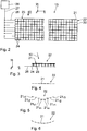
- Fig. 2 shows a highly schematic view of constructional details of the field facet mirror 13.
- An entire reflecting surface 20 of the field facet mirror 13 is divided into rows and columns so as to form a raster of separate mirrors 21.
- the individual reflecting surfaces of each of the separate mirrors 21 are plane.
- a row 22 of separate mirrors comprises a plurality of directly adjacent separate mirrors 21.
- One row 22 of separate mirrors may comprise several tens to several hundreds of the separate mirrors 21.
- the separate mirrors 21 are in the shape of a square. Other shapes of separate mirrors which allow a tiling to be achieved with as few gaps as possible are applicable as well. Such alternative shapes for separate mirrors are known from the mathematical theory of tiling.
- the field facet mirror 13 may in particular be configured as described in DE 10 2006 036 064 A1 .
- a column 23 of separate mirrors comprises a plurality of separate mirrors 21 as well.
- One column 23 of separate mirrors is for instance composed of several tens of separate mirrors 21.
- Fig. 2 shows a Cartesian xyz coordinate system which serves as a local coordinate system of the field facet mirror 13 for easier description of positional relationships. Corresponding local xyz coordinate systems can also be found in the subsequent Figures which show a plan view of the facet mirror or of a portion thereof.
- the x-axis extends horizontally towards the right and is parallel to the rows 22 of separate mirrors.
- the y-axis extends upwardly in Fig. 2 and is parallel to the columns 23 of separate mirrors.
- the z-axis is perpendicular to the drawing plane of Fig. 2 and extends out of said drawing plane.
- the reticle holder and the wafer holder are scanned synchronously in y-direction.
- a small angle between the scanning direction and the y-direction is conceivable, as will be explained below.
- the reflecting surface 20 of the field facet mirror 13 has an extension of xo in the x-direction. In the y-direction, the reflecting surface 20 of the field facet mirror 13 has an extension of yo.
- the separate mirrors 21 have x/y extensions in the range of for instance 600 ⁇ m x 600 ⁇ m to for instance 2 mm x 2 mm.
- the separate mirrors 21 may be shaped in such a way as to have a focusing effect on the illumination light 10. Such a focusing effect of the separate mirrors 21 is of particular advantage when the field facet mirror 13 is exposed to divergent illumination light 3.
- the entire field facet mirror 13 has an x 0 /y 0 extension which amounts to for instance 300 mm x 300 mm or 600 mm x 600 mm, depending on the design.
- the separate field facets 19 show typical x/y extensions of 25 mm x 4 mm or of 104 mm x 8 mm. Depending on the relationship between the size of the respective separate field facets 19 and the size of the separate mirrors 21 which form these individual field facets 19, each of the separate field facets 19 has a corresponding number of separate mirrors 21.
- Each of the separate mirrors 21 is connected to an actuator 24 for individual deflection of incident illumination light 10; this is illustrated in Fig. 2 by two dashed separate mirrors 21 which are arranged in a corner on the lefthand side below the reflecting surface 20 as well as in Fig. 3 which shows a more detailed view of a portion of a row 22 of separate facets.
- the actuators 24 are in each case arranged on a side of the separate mirrors 21 which is remote from a reflecting side of the separate mirrors 21.
- the actuators 24 may for instance be piezoelectric actuators. Designs of such actuators are known from the design of micro-mirror arrays.
- the actuators 24 of a row 22 of separate mirrors are in each case connected to a row signal bus 26 via signal lines 25.
- One row 22 of separate mirrors is allocated to a respective one of the row signal buses 26.
- the row signal buses 26 of the rows 22 of separate mirrors are in turn connected to a main signal bus 27.
- Said main signal bus 27 is connected to a control device 28 of the field facet mirror 13 via a signal.
- the control device 28 is in particular configured to actuate the separate mirrors 21 in parallel, in other words the separate mirrors 21 of one row or one column are actuated collectively.
- Each of the separate mirrors 21 is individually tiltable about two tilt axes which are perpendicular to each other, with a first one of these tilt axes being parallel to the x-axis and the second one of the two tilt axes being parallel to the y-axis.
- the two tilt axes are disposed in the separate reflecting surfaces of the respective separate mirrors 21.
- the separate mirrors 21 are individually displaceable in the z-direction by means of the actuators 24. Consequently, the separate mirrors 21 are actuable separately from each other for displacement along a normal to the reflecting surface 20.
- This allows the entire topography of the reflecting surface 20 to be changed, as is shown in a highly schematic view in Figs. 4 to 6 .
- This allows reflecting surface contours to be produced with large sagittal heights, in other words with high variations in the topography of the reflecting surface, in the form of mirror regions resembling Fresnel lenses which are all arranged in one plane.
- a division into mirror regions resembling Fresnel zones eliminates a basic curvature of such a mirror surface topography with a large sagittal height.
- Fig. 4 shows separate reflecting surfaces of the separate mirrors 21 of a section of a row 22 of separate mirrors, with all separate mirrors 21 of this row 22 of separate mirrors being set to the same absolute z-position by means of the control device 28 and the actuators 24. The result is a plane row reflecting surface of the row 22 of separate mirrors. If all separate mirrors 21 of the field facet mirror 13 are set according to Fig. 4 , the entire reflecting surface 20 of the field facet mirror 13 is plane.
- Fig. 5 shows an actuation of the separate mirrors 21 of the row 22 of separate mirrors where the central separate mirror 21 m is displaced in the negative z-direction with respect to adjacent separate mirrors 21 r1 , 21 r2 , 21 r3 .
- the EUV radiation 10 reflected by the two central separate mirrors 21 m is subject to the greatest phase offset.
- the separate mirrors 21 r3 at the edges generate the lowest phase offset.
- the separate mirrors 21 r1 , 21 r2 disposed in-between generate a phase lag which gradually becomes lower and lower with respect to the phase lag generated by the central separate mirrors 21 m .
- Fig. 6 shows an actuation of the separate mirrors 21 on the displayed section of the row 22 of separate mirrors in such a way that a convex row 22 of separate mirrors is formed on the one hand by the offset arrangement of the separate mirrors 21 relative to each other in the z-direction and on the other by orienting the separate mirrors 21 relative to each other.
- This may be useful for generating an imaging effect of separate mirror groups of the field facet mirror 13.
- a corresponding concave arrangement of groups of separate mirrors 21 is conceivable as well.
- the individual actuation of the actuators 24 via the control device 28 allows a given grouping of separate mirrors 21 to be arranged in the above-mentioned separate mirror groups each comprising at least two separate mirrors 21, with in each case one separate mirror group defining a separate field facet 19 of the field facet mirror 13.
- These separate field facets 19, which are composed of several separate mirrors 21, have the same effect as the field facets which are known for instance from US 6,438,199 B1 or US 6,658,084 B2 .
- Fig. 7 illustrates a grouping of this type, the Figure showing a section of the reflecting surface 20 of a field facet plate of an alternative embodiment of the field facet mirror 13 comprising a higher number of separate mirrors 21 compared to the illustration of Fig. 2 .
- Components which correspond to those that have already been explained above with reference to Figs. 2 to 6 have the same reference numerals and are not discussed in detail again.
- each of the separate mirror groups 19 is composed of a 24 x 3-array of separate mirrors 21, in other words it has three rows of separate mirrors of twenty-four separate mirrors 21 each. Therefore, each of the separate mirror groups 19, in other words each of the separate field facets formed by this grouping, has an aspect ratio of 8 to 1. This aspect ratio corresponds to the aspect ratio of the object field 5 to be illuminated.
- each of the separate mirror groups 19 are arranged relative to each other in such a way that the shape of each of the separate mirror groups 19 corresponds to the shape of a separate facet of a conventional field facet mirror. Consequently, each of the separate mirror groups 19 defines a separate facet.
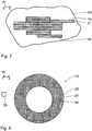
- Fig. 8 shows details of the pupil facet mirror 14 which is installed in the projection exposure apparatus 1.
- the pupil facet mirror 14 comprises a round pupil facet plate 29 which is provided with a plurality of separate mirrors 21.
- the useful separate mirrors 21 are arranged in an annular configuration about a center 30 of the pupil facet plate 29.
- An annular width of this configuration approximately corresponds to the width of eleven adjacent separate mirrors 21.
- the center 30 of the pupil facet plate 29 is provided with separate mirrors 21 which are arranged in a corresponding raster pattern as well; these separate mirrors 21 are not shown, however, as they are not in use in the annular, in other words ring-shaped, setting according to Fig. 8 .
- the separate mirrors 21 of this annular configuration are arranged in a raster pattern of rows and columns corresponding to the above-described field facet mirror 13 according to Figs. 2 to 7 .
- the separate mirrors 21 of the pupil facet mirror 14 have actuators as well and are actuated by the control device 28. These actuators and the type of the signal connection of the actuation correspond to those of the above-described field facet mirror 13.
- the separate mirrors 21 of the pupil facet mirror 14 may be grouped into separate mirror groups as well. This will hereinafter be explained by means of Figs. 14 and 15 .
- Figs. 9 to 13 show various examples of the separate mirrors 21 of the field facet mirror 13 which are grouped into separate mirror groups.
- Fig. 9 shows the case where all separate mirrors 21 of the field facet mirror 13 are grouped into a single separate mirror group 31.
- all separate mirrors 21 of the field facet mirror 13 are actuated by the control device 28 in the same way; for instance, the mirrors, which are in the same z-position, are tilted about the x-axis and about the y-axis through the same tilt angle. If each of these two tilt angles amounts to zero, the field facet mirror 13 will be a plane mirror that is composed of the separate mirrors 21.
- the total aspect ratio of the field facet mirror 13 is xo/yo.
- the field facet mirror 13 is divided into two separate mirror groups 32, 33.
- the upper separate mirror group 32 of Fig. 10 comprises the upper half of the field facet mirror 13 while the separate mirror group 33 comprises the lower half of the field facet mirror 13.
- the separate mirrors 21 of each of these two groups 32, 33 are again actuated in the same way by the control device 28. This may result in a field facet mirror comprising two separate facets which correspond to the separate mirror groups 32, 33.
- the aspect ratio of these separate facets 32, 33 is 2 xo/yo.
- the field facet mirror 13 is divided into a total of four separate mirror groups 34 to 37 which have an aspect ratio of 4 xo/yo and cover in each case the entire row width of the reflecting surface 20. Therefore, these four separate mirror groups 34 to 37 define four separate facets having the above aspect ratio.
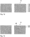
- the separate mirrors 21 of the field facet mirror 13 are divided into a total of eight separate mirror groups 38 to 45 which correspond in each case to a row of the field facet mirror 13 and have an aspect ratio of 8 xo/yo. This grouping may thus produce a field facet mirror having a total of eight separate facets.
- the separate facets 21 of the field facet mirror 13 are grouped in such a way that in each row of the field facet mirror 13, eight adjacent separate mirrors 21 are grouped into in each case one separate mirror group 46.
- Each of these separate mirror groups 46 has an aspect ratio of 8:1. If each row 22 of separate mirrors of the field facet mirror 13 is composed of for instance 80 separate mirrors 21, then each row 22 according to the grouping of Fig. 13 comprises ten separate mirror groups 46, which adds up to a total of 80 separate mirror groups 46. In the embodiment according to Fig. 13 , this allows a field facet mirror to be formed with 80 separate facets.
- Figs. 14 and 15 show an illumination of a pupil facet mirror 47, which is similar to the pupil facet mirror 14, by way of a field facet mirror which has a total of nineteen separate mirror groups which are divided into groups according to the above-explained Figs. 2 to 7 and 9 to 13 .
- the round pupil facet plate 29 of the pupil facet mirror 47 is covered with the separate mirrors 21 which form a raster pattern of rows and columns.
- Illuminated separate mirrors 21 of the pupil facet mirror 47 are indicated by hatched lines. Illumination is directed onto separate mirror groups 48 having an in each case circular boundary.
- the multiple images are arranged which are generated by the field facet mirror that is arranged upstream in the beam path of the illumination light, said multiple images being the images of a radiation source that is assumed to be circular or being the image of the image of said radiation source.
- This radiation source may be provided according to the radiation source 1 of Fig. 1 which is assumed to be circular.
- This image of said radiation source may be disposed in an intermediate focus of the beam path of the illumination and imaging light.
- These multiple images are also referred to as source images. If the image of the source in the intermediate focus of the pupil facet mirror 47 deviates from a circular shape, the shape of the separate mirror groups 48 may correspondingly be adapted to the shape of the source images.
- the separate mirror groups 48 on the pupil facet mirror 47 may have a corresponding elliptical boundary.
- Other shapes of the images of the radiation source or the source images are conceivable as well, for instance hexagonal or rectangular shapes which result in an optimal tiling on the pupil facet mirror 47.
- Such shapes of the radiation source image are achievable by a corresponding diaphragm arrangement in the intermediate focal plane.
- the illumination optics 4 may be adapted to changing shapes of the radiation source image in the intermediate faces, which are due to a change of the diaphragm, by changing the group arrangement of separate mirror groups 48 of the pupil facet mirror 47. This is also applicable when the radiation source is changed, for instance when a GDPP radiation source is replaced by an LPP radiation source.
- Each of the separate mirror groups 48 of the pupil facet mirror 47 is illuminated by exactly one separate mirror group, for instance by the separate mirror groups 19 (cf. Fig. 7 ), of the field facet mirror 13.
- the pupil facet mirror 47 is provided with a total of nineteen illuminated separate mirror groups 48.
- the upstream field facet mirror 13 is divided into nineteen allocated separate mirror groups 19. The allocation of the nineteen separate mirror groups 19 of the field facet mirror 13 to the nineteen separate mirror groups 48 on the pupil facet mirror 47 result in a total of nineteen channels for the light path of the EUV radiation 10 from the field facet mirror 13 to the object field 5.
- each of the separate mirror groups 48 of the pupil facet mirror nine central separate mirrors 21 are completely illuminated while further separate mirrors 21 surrounding the central separate mirrors 21 are partially illuminated. These at least partially illuminated separate mirrors 21 form the separate mirror group 48 which is to be actuated as a group by means of the control device 28.
- the separate mirrors 21 of each of the separate mirror groups 48 are actuated in such a way that an image of the allocated separate mirror group of the field facet mirror 13, for instance the allocated separate mirror group 19 of the embodiment according to Fig. 7 , is imaged into the object field 5 via the separate mirror group 48 of the pupil facet mirror 47 and the downstream transmission optics 16.
- the separate mirror groups 48 are approximately equally distributed across the pupil facet plate 29. Consequently, the object field 5 is illuminated by illumination angles which are distributed across the entire aperture of the pupil facet plate 29. The result is an approximately conventional illumination of the object field 5 from all directions which are defined by the image-side numerical aperture of the projection optics 7.
- Fig. 15 shows an illumination of the pupil facet mirror 47 which differs from that of Fig. 14 , in other words the illumination setting of the projection exposure apparatus 1 has been changed.
- Separate mirror groups 49 at the edge of the pupil facet plate 29 are illuminated by groupwise or collective actuation of the respective separate mirror groups of the field facet mirror 13, for instance the separate mirror group 19 according to Fig. 7 .
- the result is an approximately annular illumination angle distribution of the illumination of the object field 5 in the object plane 6.
- a minimum width of a ring of an illumination distribution, which is adjustable in this way, is defined by the width of the separate mirror groups 49.
- both the separate field facets for instance the separate mirror groups 19 of the embodiment according to Fig. 7 , and the separate mirrors 21 of the separate mirror groups 49 need to be readjusted correspondingly by tilting the respective groups using the control device 28.
- the separate mirror groups of the field facet mirror 13 on the one hand and those of the pupil facet mirror 47 on the other need to be actuated synchronously by the control device 28 when the illumination setting is changed.
- An illumination according to Fig. 15 is also possible when using the pupil facet mirror 14 according to Fig. 8 .
- Said pupil facet mirror 14 may be used to illuminate the object field with various annular illumination settings which differ by the minimum and maximum illumination angles in the object field 5.
- Fig. 16 shows another alternative version of a grouping of the separate mirrors 21 of the field facet mirror 13.
- a separate mirror group 50 of the field facet mirror 13 according to Fig. 16 is grouped in such a way that the separate mirror group 50 has an arcuate envelope 51.
- the envelope 51 is reproduced by selecting corresponding separate mirrors 21.
- the separate mirror group 50 comprises those separate mirrors 21 which are shown hatched in Fig. 16 .
- the separate mirror group 50 forms an arcuate separate facet for illuminating a correspondingly arcuate or annular object field 5 in the object plane 6.
- a plurality of such separate mirror groups 50 with arcuate or annular envelopes 51 may be formed for illuminating correspondingly formed object fields.
- the number of separate facets 21 the field facet mirror 13 needs to be provided with depends on the one hand on the desired number of separate mirror groups and on the other on the required resolution for reproducing a desired envelope, for instance the envelope 51, by means of the raster pattern or the tiling of the separate mirrors 21.
- Figs. 17 to 20 show various examples of arrangements or configurations of separate mirror groups or separate facets 19 of the field facet mirror 13. As described above with reference to Figs. 2 to 16 , each of these separate mirror groups 19 is in turn divided into a plurality of separate mirrors 21 which are not shown in detail. Each of the groupings which are shown in Figs. 17 to 20 can be generated by one and the same field facet mirror 13. The Figures show in each case only the separate mirror groups 19; the separate mirrors on the other hand, which are provided between these groups but are not in use, are not shown.
- the field facet mirror 13 is grouped into a total of four columns 52 of separate mirror groups 19.
- the field facet mirror 13 is shaded by upstream components in a central cross-shaped region 53; in this region 53, adjacent separate mirror groups 19 are arranged at a greater distance from each other so that there are no grouped separate mirrors in the region 53.
- the field facet mirror 13 according to Fig. 18 is grouped in such a way that the separate mirror groups 19, which are in turn composed of a plurality of separate mirrors (not shown), are arranged in columns which are offset relative to each other in the way that is illustrated by the section shown in Fig. 7 .
- a horizontal central portion 54 of the field facet mirror 13 that increases in width in the center is not covered with grouped separate mirrors 21.
- the portion 54 is shaded by components, which are arranged upstream of the field facet mirror 13 according to Fig. 18 , as well.
- the separate mirror groups 19 are arranged in supergroups 55. Some of the adjacent supergroup rows are offset relative to each other to form a circular envelope of the field facet mirror 13 according to Fig. 18 .
- the separate mirror groups 19 of the field facet mirror 13 according to Figs. 17 and 18 have an aspect ratio x/y of 13:1. These separate mirror groups 19 may therefore be formed by 13 adjacent square-shaped separate mirrors 21.
- Fig. 19 shows an example of a configuration of a plurality of arcuate or annular separate mirror groups 50, with each separate mirror group 50 corresponding to that which has been described above with reference to Fig. 16 .
- the separate mirror groups 50 in other words the separate facets of the field facet mirror 13 according to Fig. 19 , are arranged in supergroups 56 of ten separate mirror groups 50 each which are arranged one above the other in Fig. 19 .
- the supergroups 56 are in turn arranged in five supergroup columns.
- the supergroups 56 are arranged symmetrically, which allows them to be inscribed in a circular envelope 57.
- Fig. 20 shows another configuration of the field facet mirror 13 which is divided into arcuate or annular separate mirror groups 50.
- the separate mirror groups 50 are in turn grouped into supergroups 58 which comprise in each case a different number of separate mirror groups 50.
- the supergroup 58a shown on the bottom left of Fig. 20 is for instance divided into nine separate mirror groups 50.
- Other supergroups 58 have more or less separate mirror groups 50. Due to a central shading formed by the collector 11, a central portion 59 of the field facet mirror 13 is not provided with separate mirror groups 13.
- Figs. 21 and 22 show various divisions of the pupil facet mirror 47 into separate mirror groups 60, 61. Again, the Figures show only the separate mirror groups; the separate mirrors between the grouped separate mirrors are not shown. The divisions according to Figs. 21 and 22 are achievable using one and the same pupil facet mirror 47.
- the pupil facet mirror 47 is divided into separate mirror groups 60 which form a plurality of concentric circles about a central region 62.
- Each of the separate mirror groups 60 is in turn composed of a plurality of separate mirrors 21 of the pupil facet mirror 47, as explained above with reference to Figs. 8 , 14 and 15 .
- the pupil facet mirror 47 comprises a total of more than 100 separate mirror groups 60; in the embodiment according to Fig. 21 , the number of separate mirrors 21 amounts to more than 1.000.
- the separate mirrors 21 according to Fig. 22 are grouped in such a way that the round separate mirror groups 61 are arranged in an approximate hexagonal-close packing.
- Figs. 21 and 22 have proven to be particularly suitable for forming illumination settings with a given illumination angle distribution. If required, some of the separate mirror groups 60, 61 or supergroups thereof may be blocked out by tilting their upstream separate mirror groups 19 of the field facet mirror 13 for defining a particular illumination setting.
- Fig. 23 shows a tiling of the reflecting surface 20 of one of the above-described facet mirrors which is covered with separate mirrors 21.
- the separate mirrors 21 of the tiling according to Fig. 23 are square-shaped as well.
- the separate mirrors 21 are not arranged in a raster pattern of rows and columns but adjacent columns are offset relative to each other by half an edge length of the separate mirrors 21.
- the tiling according to Fig. 23 allows arcuate or annular separate mirror groups, for instance the separate mirror groups 50 according to Figs. 19 and 20 , to be formed with low losses next to the envelope 51, which requires a lower separate mirror or pixel resolution at a given maximum allowable loss than a tiling which is arranged in a raster pattern of rows and columns.
- Fig. 24 shows a projection exposure apparatus 1 comprising an alternative illumination optics.
- Components which correspond to those which have already been explained above with reference to Figs. 1 to 23 have the same reference numerals and are not discussed in detail again.
- the first element downstream of the radiation source 3 is a bundle-forming collector 63 which otherwise has the function of the collector 11 in the arrangement according to Fig. 1 .
- Downstream of the collector 63 is arranged a specular reflector 64.
- Said specular reflector 64 forms the incident EUV radiation 10 in such a way that the EUV radiation 10 illuminates the object field 5 in the object plane 6, which results in a given, for instance homogeneously illuminated, pupil illumination distribution with a circular boundary, in other words a corresponding illumination setting, in the pupil plane 65 of the projection optics not shown in Fig. 24 , said pupil plane 65 being arranged downstream of the reticle.
- the effect of the specular reflector 65 is described in US 2006/0132747 A1 .
- a reflecting surface of the specular reflector 64 is divided into separate mirrors 21. Depending on the illumination requirements, these separate mirrors of the specular reflector 64 are grouped into separate mirror groups, in other words into facets of the specular reflector 64.
- Fig. 25 shows an alternative illumination of the pupil facet mirror 14 which is different from the illumination according to Fig. 1 .
- Components which correspond to those which have been explained above with reference to Figs. 1 to 23 have the same reference numerals and are not discussed in detail again.
- the illumination system 2 is shown up to and including the pupil facet mirror 14.
- the illumination system 2 according to Fig. 25 is not provided with an intermediate focal plane between the collector 11 and the field facet mirror 13.
- the reflecting surfaces of the separate mirror groups of the field facet mirror 13, which are not shown in more detail in Fig. 25 may be plane surfaces.
- the actuation of some of the separate mirrors 21 can be individually different from that of the remaining separate mirrors 21 of this group, in other words they can be taken out of the separate mirror group. Consequently, the various separate facets of the field facet mirror 13 which are thus formed can individually be provided with specific blockings or shadings, which may be useful for correcting the homogeneity of the illumination intensity in the object field 5.
- the actuation of some of the separate mirrors 21 can be individually different from that of the other separate mirrors 21 of this group, in other words they are taken out of the separate mirror group.
- the various source images (cf. 48 in Figs. 14 and 15 ) on the pupil facet mirror 14, 47 can be blocked out individually by means of specific blockings or shadings. This may be useful for correcting or for setting particular intensity distributions across the illumination angles of the object field 5.
- Fig. 26 shows another embodiment of an illumination optics. Components and functions which correspond to those that have been explained above with reference to Figs. 1 to 25 have the same reference numerals and are not discussed in detail again.
- the first element downstream of the radiation source 3 is a collector 66 with a continuous mirror surface which is, in other words, not provided with facets.
- the mirror surface may for instance be an elliptical mirror surface.
- the collector 66 may be replaced by a nested collector.
- the EUV radiation 10 Downstream of the intermediate focal plane 12, the EUV radiation 10 impinges upon a collector facet mirror 67.
- Said collector facet mirror 67 has a plane carrier plate 68 which is joined to an x/y array of ellipsoidal separate mirrors 69 that is fastened thereon.
- the ellipsoidal separate mirrors 69 have closely adjacent reflecting surfaces, causing the largest part of the EUV radiation 10 to be reflected by the ellipsoidal separate mirrors 69 of the collector facet mirror 67.
- the ellipsoidal separate mirrors 69 are connected to actuators (not shown) which allow the ellipsoidal separate mirrors 69 to be tilted individually.
- the ellipsoidal separate mirrors 69 are formed in such a way that they all absorb the same solid angle of the EUV radiation 10.
- the radiation source 3 is disposed in one focal point of the elliptical collector 66 while the intermediate focus of the intermediate focal plane 12 is disposed in the other focal point thereof.
- a specular reflector 70 Downstream of the collector facet mirror 67, a specular reflector 70 is arranged in the beam path of the EUV radiation 10, the specular reflector 70 comprising an x/y-array of separate mirrors 21.
- Each ellipsoidal separate mirror 69, which is impinged by the EUV radiation 10 is allocated to one of the separate mirrors 21 of the specular reflector 70 in the subsequent beam path, causing the EUV radiation 10 to be divided into a number of radiation channels corresponding to the number of impinged ellipsoidal separate mirrors 69, with each of these radiation channels impinging upon one of the ellipsoidal separate mirrors 69 and then upon the respectively allocated separate mirror 21 of the specular reflector 70.
- the intermediate focus of the intermediate focal plane 12 is disposed in a respective one of the focal points of one of the ellipsoidal separate mirrors 69 while in the second focal point of the ellipsoidal separate mirror 69 is disposed the separate mirror 21 of the specular reflector 70 which is allocated to said ellipsoidal separate mirror 69.
- the specular reflector 70 is disposed in an image plane 71 for source images 72 of the radiation source 3. These source images 72 are discretely arranged in the image plane 71, in other words they are arranged at a distance from each other. This is shown in Fig. 28 which is a plan view of the source images 72 at the location of the specular reflector 70.
- an envelope of the total of source images 72 approximately has the shape of a kidney or a bean.
- object field portions 73 of the object field 5 in the object plane 6, in which is arranged the reticle are illuminated via the individual radiation channels.
- the object field portions 73 cover the object field 5 in the manner of a generally distorted, rectangular x/y raster pattern.
- the object field portions 73 are also referred to as source spots as they are allocated to in each case one source image 72.
- the illuminated shape of the object field portions 73 is correlated with the boundary shape of the ellipsoidal separate mirrors 69.
- the specular reflector 70 is not arranged in a pupil plane of the illumination optics according to Fig. 26 .
- the object field 5 has a partially annular shape for instance with a slot width of 8 mm in the y-direction and a width of 104 mm in the x-direction.
- the separate mirrors 21 of the specular reflector 70 form the radiation channels of the EUV radiation in such a way that the object field, which is formed by the object field portions 73, is illuminated in the object plane 6, and that a desired intensity distribution is obtained in a downstream pupil plane of the illumination optics which coincides with a pupil plane of the downstream projection optics, thus ensuring that a desired illumination angle distribution is obtained on the reticle.
- Fig. 26 is a schematic outline of a channel-by-channel illumination where adjacent ellipsoidal separate mirrors 69 cause EUV radiation 10 to impinge upon adjacent separate mirrors 21 of the specular reflector 70.
- adjacent relation is not compulsory.
- This is hereinafter also referred to as mixing of proximity relationships which is illustrated in Fig. 27 showing an alternative relation of the ellipsoidal separate mirrors 69 to the separate mirrors 21 of the specular reflector 70.
- a mixed allocation of the ellipsoidal separate mirrors 69 to the separate mirrors 21 of the specular reflector 70 may for instance take place using algorithms which are disclosed in US 6,438,199 B1 . This allocation may for instance be cross-wise, with the result that adjacent separate mirrors 21 of the specular reflector 70 are impinged with light from non-adjacent ellipsoidal separate mirrors 69.
- the number of separate mirrors 21 of the specular reflector 70 exceeds the number of ellipsoidal separate mirrors 69 of the collector facet mirror 67. In this way, the actuators of the ellipsoidal separate mirrors 69 can be actuated in such a way that various subgroups of the separate mirrors 21 of the specular reflector 70 are adjusted to achieve various desired illuminations of the object field 5.
- Each of the source images 72 may be generated on exactly one of the separate mirrors 21.
- the separate mirrors 21 of the specular reflector 70 are in each case connected to actuators as well, which allows them to be individually tilted relative to the image plane 71. After adjusting the ellipsoidal separate mirrors 69, this enables one to accordingly readjust the separate mirrors 21 of the specular reflector 70.
- Figs. 26 and 27 show a schematic view of a group 74 of ellipsoidal separate mirrors 69 which extend along the y-direction and are allocated to a group 75 of separate mirrors 21 of the specular reflector 70 and to a group of object field points 73, the group 75 of separate mirrors 21 and the group of object field points 73 extending along the y-direction as well.
- the actuators of the collector facet mirror 67 on the one hand and the specular reflector 70 on the other are actuable in such a way that the ellipsoidal separate mirrors 69 or the separate mirrors 21 of the specular reflector 70 are actuable in groups. Such an actuation of particular groups is however not compulsory.
- the collector facet mirror 67 may be assembled from ellipsoidal separate mirrors 69 which are prefabricated separately. Another method of producing the collector facet mirror 67 allows said collector facet mirror 67 to be formed monolithically, for instance through single-diamond processing. The collector facet mirror 67 is then smoothed out by means of HSQ or polyamide spin-coating.
- the HSQ method is described in Farhad Salmassi et al., Applied Optics, Volume 45, no. 11, p. 2404 to 2408 .
- collector facet mirror 67 Another method of producing the collector facet mirror 67 allows the collector facet mirror 67 to be galvanically formed from a base body by means of electroplating.
- the radiation source 3, the collector 66 and the collector facet mirror 67 may be integrated in a multisource array.
- a multisource array of this type is described in German patent application no. 10 2007 008 702.2 , which is to be regarded as fully incorporated in this application.
- each radiation source of the multisource array is only able to illuminate a partial region, in other words an object field portion.
- the ellipsoidal separate mirror 69 or if the separate mirrors 21 are curved, even the separate mirrors 21 of the embodiments explained above, may in turn be configured of a plurality of plane micro mirrors, with said plurality of plane surfaces approximating the respective curved surface of the ellipsoidal separate mirror 69 or of the curved separate mirror 21 in such a way as to resemble a polyhedron.
- the micro mirrors which approximate the curved surfaces of the ellipsoidal separate mirrors 69 or of the curved separate mirrors 21, may in turn be displaceable by means of actuators.
- the micro mirrors may be used to influence the imaging properties of the separate mirrors 69, 21.
- Micro mirrors of this type may for instance be designed like a micro mirror array (MMA) in which the separate mirrors are movably mounted using laterally attached spring joints, and which are actuable electrostatically.
- Micro mirror arrays of this type which are for instance disclosed in EP 1 289 273 A1 , are known to those skilled in the art as "MEMS" (Micro-electromechanical systems).
- the separate mirrors 21 and 69 provide illumination channels for superimposing the EUV radiation 10, in other words the illumination light, in the object field 5 of the projection exposure apparatus 1.
- illumination channels AK are illustrated schematically in Figs. 26 and 27 .
- Corresponding illumination channels are also found in the embodiments according to Figs. 1 to 25 .
- the separate mirrors 21 and 69 have mirror surfaces with such an extension that these separate-mirror illumination channels illuminate object portions in the object field 5 which are smaller than the object field 5. This is schematically shown in Figs. 26 and 27 for the specular reflector 70.
- This illumination of the object field 5 by assembling object field portions which are allocated to different separate-mirror illumination channels is generally also applicable in the embodiments according to Figs. 1 to 25 .
- Fig. 29 is a schematic view of an exemplary object field 5 which is illuminated by a total of twenty-two illumination channels, with said illumination channels illuminating a corresponding number of twenty-two object field portions 76. Boundaries 77, 78 between the object field portions 76 extend in the x-direction or in the y-direction, respectively.
- a scanning direction y scan in which the wafer holder and the reticle holder are synchronously displaced during the projection exposure using the projection exposure apparatus 1 with the object field illumination according to Fig. 29 , is not exactly parallel to the y-direction, in other words it is not perpendicular to the long field axis x of the object field 5, but is tilted relative to said field axis x through an angle ⁇ . Consequently, when scanned through the object field 5, a point on the reticle sees, if at all, one of the boundaries 78, which extend in y-direction and between two object field portions 76, only during a part of the scanning process.
- the object field portions may be arranged in such a way that there are no continuous boundaries between the object field points along a scanning direction.
- Such an arrangement of superimposed object field portions which are offset relative to each other is for instance obtained if the object field 5, corresponding to an arrangement according to Fig. 23 which is rotated through 90°, is illuminated using object field portions which correspond to the separate facets 21 according to Fig. 23 .
- there are rows of object field portions which are offset relative to each other perpendicular to the scanning direction with the result that even if the scanning direction y scan coincides exactly with the y-direction, there is no single point on the reticle which moves along a boundary between object field portions all the time when scanned through the object field 5. Therefore, an offset arrangement of this type also helps to avoid unwanted inhomogeneities of the intensity to which the field points are exposed during the scanning process.
- a corresponding homogenization may be obtained if the object field portions have boundary shapes with edges that are not parallel to the scanning direction. This may be for instance be achieved by trapezoidal or rhombic separate mirrors 21 whose shape defines the shape of the object field portions.
- the transmission optics 15 may be configured in such a way that sharp edges of the images of the separate mirrors 21, 69 are generated upstream or downstream of the object plane 6.
- the separate mirrors 21, 69 may have a multilayer coating comprising separate layers of molybdenum and silicon in order to optimize the reflectivity of the separate mirrors 21, 69 for the EUV wavelength that is used.
- the separate-mirror illumination channels may be transmitted to the object field 5 in groups by one and the same pupil facet.
- Each of these pupil facets defines a group illumination channel which combines the separate-mirror illumination channels allocated to this pupil facet.
- the number of group illumination channels then corresponds to the number of pupil facets which are not divided into separate mirrors.
- each of these pupil facets and each group illumination channel is then allocated to a number of separate mirrors of the field facet mirror. In order to modify illumination angle distributions, the number of the pupil facets may exceed the number of the group illumination channels.
- adjacent separate mirrors 21 of the field facet mirror need not be transmitted via adjacent pupil facet separate mirrors (compare the above descriptions of the specular reflector according to Figs. 26 and 27 ); in fact, groups of field-facet separate mirrors and pupil-facet separate mirrors may be provided which are randomly mixed in space for combined illumination of the entire object field 5.
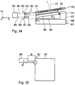
- the separate mirror 21 according to Figs. 31 to 34 has a mirror body 79 in the form of a mirror plate.
- the mirror body 79 consists of silicon.
- the mirror body 79 has a rectangular reflecting surface 80, which is approximately square-shaped in the embodiment according to Figs. 30 to 34 , for reflecting the EUV radiation 10.
- the reflecting surface 80 may be provided with a multilayer reflecting coating for optimizing the reflectivity of the separate mirror 21 for EUV radiation 10.
- the mirror body 79 of the separate mirror 21 is tiltable about two tilt axes relative to a rigid carrier body consisting of silicon. These two tilt axes are denoted by w 1 and w 2 in Figs. 30 to 34 . Each of these two tilt axes w 1 , w 2 is part of a tilt joint 82, 83 which is in each case a solid joint. The two tilt axes w 1 , w 2 are perpendicular to each other. The tilt axis w 1 is parallel to the x-axis while the tilt axis w 2 is parallel to the y-axis.
- the mirror body 70 and the carrier body 81 may also be formed of FiO 2 or Fi 3 N 4 .
- the tilt axis w 2 is disposed in the extension plane of the mirror body 79.
- a small dead surface area 83a which is not tiltable, the dead surface area 83a being shown in Fig. 30 above the tilt axis w 2 .
- Both of the two tilt axes w 1 , w 2 extend parallel to the plane of the reflecting surface 80.
- the tilt joints 82, 83 may also be arranged in such a way that at least one of the two tilt axes w 1 , w 2 is disposed in the plane of the reflecting surface 80.
- EUV and high-vacuum compatible materials which are suitable for forming the separate mirror 21, include CVD (chemical vapor deposition) diamond, SiC (silicon carbide), SiO 2 (silicon oxide), Al 2 O 3 , copper, nickel, aluminum alloys and molybdenum.
- CVD chemical vapor deposition
- SiC silicon carbide
- SiO 2 silicon oxide
- Al 2 O 3 copper, nickel, aluminum alloys and molybdenum.
- Fig. 32 shows an enlarged view of the tilt joint 82 of the tilt axis w 1 .
- the tilt joint 83 is formed correspondingly.
- the tilt joint 82 Perpendicular to the tilt axis w 1 , in other words in the z-direction of Fig. 32 , the tilt joint 82 has a joint thickness S. Along the tilt axis w 1 , in other words in the x-direction of Fig. 32 , the tilt joint 82 has a joint length L (cf. Fig. 33 ). The size of the joint length L is comparable with a transverse extension of the mirror body 79.
- the joint length L amounts to approximately 1 mm.
- the joint thickness S which is excessively large in the drawing, amounts to 1 ⁇ m.
- the quotient L/S therefore amounts to approximately 1000.
- the mirror body 79 is connected in one piece with an intermediate carrier body 84 via the tilt joint 83 whose dimensions, in particular the joint thickness S and the joint length L thereof, correspond to those of the tilt joint 82.
- the intermediate carrier body 84 also consists of silicon.
- the intermediate carrier body 84 is L-shaped and has a joint portion 85 which is directly adjacent to the tilt joint 83, and a plate portion 86 which is arranged below the mirror body 79, in other words on the side of the mirror body 79 remote from the reflecting surface 80.
- there is a distance B between the mirror body 79 and the joint portion 85 of the intermediate carrier body 84 which distance B is also referred to as width of the tilt joint 83.
- the plate portion 86 of the intermediate carrier body 84 is connected in one piece with a joint portion 87 of the carrier body 81 via the tilt joint 82.
- the joint portion 87 is fastened to a plate portion 88 of the carrier body 81.
- the plate portion 88 of the carrier body 81 is arranged below the plate portion 86 of the intermediate carrier body 84. In the neutral position shown in Figs. 31 and 33 , the mirror body 79, the plate portion 86 of the intermediate carrier body 84 and the plate portion 88 of the carrier body 81 are parallel to each other.
- Two electrode actuators 89, 90 are provided for controlled tilting of the mirror body 79 about the two tilt axes x 1 , x 2 (cf. Fig. 34 ).
- the electrode actuator 89 is allocated to the tilt joint 82 and is therefore also referred to as wi-actuator 90.
- the electrode actuator 90 is allocated to the tilt joint 83 and is therefore also referred to as w 2 -actuator.
- the first electrode of the w 2 -actuator is the mirror body 79 itself which is electrically conductive.
- a counter electrode 91 of the w 2 -actuator 90 is a conductive coating that is applied to the plate portion 86 of the intermediate carrier body 84, the coating facing the mirror body 79. In the neutral position of the separate mirror 21, the counter electrode 79 has a distance from the mirror body 79 of approximately 100 ⁇ m.
- the two electrodes 90, 91 of the w 2 -actuator are connected to an actuable voltage source 93 via signal lines 92.
- the voltage source 93 is connected to an actuator control device 95 via a signal line 94.
- the counter electrode 91 is at the same time an electrode of the wi-actuator 89.
- a counter electrode 96 of the wi-actuator 89 is formed by a conductive coating that is applied to the plate portion 88 of the carrier body 81.
- the counter electrode 96 of the wi-actuator 89 is arranged on the side of the plate portion 88 of the carrier body 81 facing the plate portion 86 of the intermediate carrier body 84. In the neutral position, in other words in a force-free state, the distance of the counter electrode 96 of the wi-actuator 89 from the plate portion 86 of the intermediate carrier body 84 amounts to 100 ⁇ m.
- the electrodes 91, 96 are electrically connected to another voltage source 97 via signal lines 92.
- the voltage source 97 is connected to the actuator control device 95 via another control line 98.
- the plate portion 86 of the intermediate carrier body 84 is controllably tiltable about the tilt axis w 1 towards the plate portion 88 of the carrier body 81, and the mirror body 79 is controllably tiltable about the tilt axis w 2 relative to the plate portion 86 of the intermediate carrier body 84 through in each case a given tilt angle.
- the modulus of the tilt angle about the respective tilt axis w 1 , w 2 depends, among other things, on the dimensions of the tilt joints 82, 83, on the surface area of the electrodes 90, 91, 96, on their distance from each other, and of course on the magnitude of the applied voltages VI, V2.
- the applied voltages VI, V2 allow the tilt angle to be continuously adjusted about the two tilt axes w 1 , w 2 .
- Fig. 34 shows a tilted position in which the plate portion 86 of the intermediate carrier body 84 has been tilted relative to and towards the plate portion 88 of the carrier body 81 about the tilt axis w 1 on the one hand, and the mirror body 79 has been tilted relative to and towards the plate portion 86 of the intermediate carrier body 84 about the tilt axis w 2 on the other after applying the voltages VI, V2.
- Incident EUV radiation 10 is deflected by the reflecting surface 80 of the mirror body 79 in a defined manner, as outlined in Fig. 34 .
- Fig. 35 is an alternative view of Fig. 32 , showing the dimensional relationships in an embodiment of the tilt joint 82.
- a joint thickness S also amounts to approximately 1 ⁇ m
- a joint width B to approximately 20 ⁇ m
- a joint length L which is perpendicular to the drawing plane of Fig. 35 , amounts to approximately 1 mm.
- Figs. 36 and 37 show another embodiment of an actuator 119 for controlled tilting of the reflecting surface 80 of for instance the individual mirror 21 about the at least one tilt axis w 1 , w 2 .
- Components which correspond to those that have already been explained above with reference to Figs. 30 to 35 have the same reference numerals and are not discussed in detail again.
- the actuator 119 has a movable electrode 120 whose free end 121 (cf. Figs. 36 and 37 ) is provided with a tilt joint which is allocated to the actuator 119 so as to establish a movable connection with a joint body which is not shown in Figs. 36 and 37 .
- the movable electrode 120 is flat and shown in cross-section in Figs. 36 and 37 . In the cross-sectional view according to Figs. 36 and 37 , the movable electrode 120 is curved.
- a counter electrode 22 of the actuator 119 is rigidly connected with the plate portion 88 of the carrier body 81.
- the counter electrode 122 is for instance a coating that is applied to the plate portion 88 of the carrier body 81.
- a layer in the form of a dielectric 123 is arranged between the movable electrode 120 and the counter electrode 122.
- the dielectric 123 may be a flat coating on the counter electrode 122.
- the counter electrode 122 is in direct contact with the movable electrode 120 in a contact region 124.
- a distance region 125 of the movable electrode 120 is spaced from the counter electrode 122 and from the dielectric 123.
- the free end 121 of the movable electrode 120 is part of the distance region 125.
- Figs. 36 and 37 show two positions of the movable electrode 120.
- Fig. 36 shows a neutral position in which no voltage is applied between the two electrodes 120, 122.
- the free end 121 of the movable electrode 120 is then disposed at a maximum distance from the plate portion 88.
- Fig. 37 shows the position in which a tilting voltage of approximately 80 V is applied between the electrodes 120, 122.
- Such actuators 119 according to Figs. 36 and 37 are also referred to as micro-scroll drives.
- tilt joints may have a different dimensional relationship of the joint length L to the joint thickness S.
- L/S may be larger than 50, larger than 100, larger than 250 or even larger than 500.
- An L/S relationship of larger than 1000 is conceivable as well.
- the above explained actuators for tilting the mirror body 79 may comprise an integrated sensor for measuring the respective tilt angle about the tilt axes w 1 , w 2 .
- This sensor may in particular be used for monitoring the preset tilting angle.
- Figs. 38 and 39 shows further embodiments of tilings on the reflecting surface 20 of one of the facet mirrors described above comprising separate mirrors 21.
- the separate mirrors 21 of adjacent columns are offset relative to each other in the y-direction.
- Adjacent separate mirrors 21 of a separate mirror group 19 which are arranged in these columns S1, S2 are in each case offset relative to each other in the y-direction by half the y-extension of the separate mirrors 21.
- separate mirrors 21 of a separate mirror group 19 which are arranged next to each other in these columns are in each case offset relative to each other in the y-direction by a full y-extension of the separate mirrors 21.
- This offset allows a given large radius of curvature of the separate mirror groups 19 to be achieved despite the comparatively large y-extension of the respective separate mirrors 21.
- the separate mirror group 19 may be adapted to a curved object field shape.
- One of the separate mirror groups 19 at the edge of Fig. 38 is highlighted to be more easily identifiable.
- Fig. 39 shows another embodiment of an arrangement of separate mirrors 21 and an alternative grouping of these separate mirrors 21 into separate mirror groups 19.
- the separate mirror groups 19, which are only partially shown in the x-direction of Fig. 39 have an x/y aspect ratio which corresponds to that of the separate mirror groups 19 according to Fig. 38 .
- the separate mirror groups 19 according to Fig. 39 are of rectangular shape.
- Each of these separate mirror groups 19 according to Fig. 39 may illuminate a rectangular object field. It is conceivable as well to illuminate an arcuate object field using the rectangular separate mirror groups 19 according to Fig. 39 ; in this case, the grazing incidence mirror 18, for instance, (cf. Fig. 1 ) will then ensure a corresponding field formation.
- Each of the separate mirror groups 19 comprises seven rows of adjacent separate mirrors 21 which are arranged one above the other. Joints 140 between these rows are continuously horizontal, in other words they extend in the x-direction. Joints 141 between adjacent separate mirrors 21 in one of the rows are arranged at an angle T relative to the y-direction, i.e. relative to the direction of the column arrangement of the separate mirrors 21. In the illustrated embodiment, the angle T amounts to approximately 12°. Other joint angles T are conceivable as well, for instance joint angles T of 5°, 8°, 15°, 19° or 20°.
- Each of the separate mirrors 21 has an x/y aspect ratio which corresponds to the x/y aspect ratio of the separate mirrors 19. According to Fig. 39 , this seems not to be the case; this is due to the fact that the separate mirrors 21 are shown in a compressed view when seen in the x-direction.
- the projection exposure apparatus 1 is used to image at least a part of the reticle in the object field 5 onto a region of a light-sensitive layer on the wafer in the image field 8 for lithographic production of a micro- or nanostructured component, in particular a semiconductor component such as a microchip.
- the reticle and the wafer are displaced in the y-direction in a temporally synchronized manner, namely either continuously when operating in the scanner mode or incrementally when operating in the stepper mode.
- a defined setting of tilt angles for the separate mirrors 21 and 69 allows an intensity scanning profile, in other words an intensity distribution, of the imaging light 10 to be defined across the image field 8 in the y-direction if these separate mirrors 21 and 69 are not arranged in field planes of the illumination optics.
- a scanning profile of this type may be a function of the y-coordinate resembling a Gaussian distribution.
- a scanning profile of this type may be a function of the y-coordinate in the shape of a trapezoid.
- An alternative scanning profile of this type may also be obtained by convolving a rectangular function with a Gaussian function.
Landscapes
- Physics & Mathematics (AREA)
- General Physics & Mathematics (AREA)
- Optics & Photonics (AREA)
- Exposure And Positioning Against Photoresist Photosensitive Materials (AREA)
- Exposure Of Semiconductors, Excluding Electron Or Ion Beam Exposure (AREA)
- Lenses (AREA)
- Mounting And Adjusting Of Optical Elements (AREA)
- Optical Elements Other Than Lenses (AREA)
Applications Claiming Priority (5)
| Application Number | Priority Date | Filing Date | Title |
|---|---|---|---|
| US2893108P | 2008-02-15 | 2008-02-15 | |
| DE102008009600A DE102008009600A1 (de) | 2008-02-15 | 2008-02-15 | Facettenspiegel zum Einsatz in einer Projektionsbelichtungsanlage für die Mikro-Lithographie |
| US14345609P | 2009-01-09 | 2009-01-09 | |
| DE200910000099 DE102009000099A1 (de) | 2009-01-09 | 2009-01-09 | Mikrospiegelarray mit Doppelbiegebalken Anordnung und elektronischer Aktorik |
| PCT/EP2009/000825 WO2009100856A1 (en) | 2008-02-15 | 2009-02-06 | Facet mirror for use in a projection exposure apparatus for microlithography |
Publications (2)
| Publication Number | Publication Date |
|---|---|
| EP2243047A1 EP2243047A1 (en) | 2010-10-27 |
| EP2243047B1 true EP2243047B1 (en) | 2021-03-31 |
Family
ID=40602234
Family Applications (1)
| Application Number | Title | Priority Date | Filing Date |
|---|---|---|---|
| EP09709960.0A Active EP2243047B1 (en) | 2008-02-15 | 2009-02-06 | Facet mirror for use in a projection exposure apparatus for microlithography |
Country Status (7)
| Country | Link |
|---|---|
| US (2) | US9411241B2 (ja) |
| EP (1) | EP2243047B1 (ja) |
| JP (3) | JP5487118B2 (ja) |
| KR (2) | KR101591610B1 (ja) |
| CN (2) | CN103293665B (ja) |
| TW (2) | TWI639892B (ja) |
| WO (1) | WO2009100856A1 (ja) |
Families Citing this family (163)
| Publication number | Priority date | Publication date | Assignee | Title |
|---|---|---|---|---|
| US7843632B2 (en) * | 2006-08-16 | 2010-11-30 | Cymer, Inc. | EUV optics |
| CN103293665B (zh) | 2008-02-15 | 2016-07-06 | 卡尔蔡司Smt有限责任公司 | 微光刻的投射曝光设备使用的分面镜 |
| DE102009000099A1 (de) * | 2009-01-09 | 2010-07-22 | Carl Zeiss Smt Ag | Mikrospiegelarray mit Doppelbiegebalken Anordnung und elektronischer Aktorik |
| DE102009045135A1 (de) * | 2009-09-30 | 2011-03-31 | Carl Zeiss Smt Gmbh | Beleuchtungsoptik für die Mikrolithographie |
| DE102009045694B4 (de) | 2009-10-14 | 2012-03-29 | Carl Zeiss Smt Gmbh | Beleuchtungsoptik für die Mikrolithographie sowie Beleuchtungssystem und Projektionsbelichtungsanlage mit einer derartigen Beleuchtungsoptik |
| DE102009054540B4 (de) * | 2009-12-11 | 2011-11-10 | Carl Zeiss Smt Gmbh | Beleuchtungsoptik für die EUV-Mikrolithographie |
| DE102009054888A1 (de) * | 2009-12-17 | 2011-06-22 | Carl Zeiss SMT GmbH, 73447 | Optisches Element mit einer Mehrzahl von refletiven Facettenelementen |
| NL2005771A (en) * | 2009-12-29 | 2011-06-30 | Asml Netherlands Bv | Illumination system, lithographic apparatus and illumination method. |
| DE102010001388A1 (de) * | 2010-01-29 | 2011-08-04 | Carl Zeiss SMT GmbH, 73447 | Facettenspiegel zum Einsatz in der Mikrolithografie |
| EP2542941B1 (en) * | 2010-03-05 | 2015-05-06 | Micronic Mydata AB | 1.5d slm for lithography |
| DE102011004615A1 (de) * | 2010-03-17 | 2011-09-22 | Carl Zeiss Smt Gmbh | Beleuchtungsoptik für die Projektionslithografie |
| DE102010029651A1 (de) | 2010-06-02 | 2011-12-08 | Carl Zeiss Smt Gmbh | Verfahren zum Betrieb einer Projektionsbelichtungsanlage für die Mikrolithographie mit Korrektur von durch rigorose Effekte der Maske induzierten Abbildungsfehlern |
| DE102011085132A1 (de) | 2010-11-24 | 2012-05-24 | Carl Zeiss Smt Gmbh | Optische Baugruppe für die Projektionslithografie |
| DE102010062720B4 (de) | 2010-12-09 | 2012-07-12 | Carl Zeiss Smt Gmbh | EUV-Lithographiesystem |
| DE102011003928B4 (de) * | 2011-02-10 | 2012-10-31 | Carl Zeiss Smt Gmbh | Beleuchtungsoptik für die Projektionslithographie |
| DE102011004326A1 (de) | 2011-02-17 | 2012-08-23 | Carl Zeiss Smt Gmbh | Optische Baugruppe für eine Beleuchtungsoptik für die Projektionslithographie |
| DE102011005840A1 (de) | 2011-03-21 | 2012-09-27 | Carl Zeiss Smt Gmbh | Steuerbare Mehrfachspiegelanordnung, optisches System mit einer steuerbaren Mehrfachspiegelanordnung sowie Verfahren zum Betreiben einer steuerbaren Mehrfachspiegelanordnung |
| CN103443863B (zh) * | 2011-03-23 | 2017-03-08 | 卡尔蔡司Smt有限责任公司 | Euv反射镜布置、包括euv反射镜布置的光学系统以及操作包括euv反射镜布置的光学系统的方法 |
| DE102011005940A1 (de) | 2011-03-23 | 2012-09-27 | Carl Zeiss Smt Gmbh | EUV-Spiegelanordnung, optisches System mit EUV-Spiegelanordnung und Verfahren zum Betreiben eines optischen Systems mit EUV-Spiegelanordnung |
| DE102011077234A1 (de) | 2011-06-08 | 2012-12-13 | Carl Zeiss Smt Gmbh | EUV-Spiegelanordnung, optisches System mit EUV-Spiegelanordnung und Verfahren zum Betreiben eines optischen Systems mit EUV-Spiegelanordnung |
| DE102011006100A1 (de) * | 2011-03-25 | 2012-09-27 | Carl Zeiss Smt Gmbh | Spiegel-Array |
| WO2012139649A1 (en) | 2011-04-14 | 2012-10-18 | Carl Zeiss Smt Gmbh | Facet mirror device |
| DE102011076297A1 (de) * | 2011-05-23 | 2012-11-29 | Carl Zeiss Smt Gmbh | Blende |
| US8681413B2 (en) | 2011-06-27 | 2014-03-25 | Kla-Tencor Corporation | Illumination control |
| DE102011078928A1 (de) * | 2011-07-11 | 2013-01-17 | Carl Zeiss Smt Gmbh | Beleuchtungsoptik für die Projektionslithografie |
| DE102011080052A1 (de) | 2011-07-28 | 2013-01-31 | Carl Zeiss Smt Gmbh | Spiegel, optisches System mit Spiegel und Verfahren zur Herstellung eines Spiegels |
| DE102011082065A1 (de) | 2011-09-02 | 2012-09-27 | Carl Zeiss Smt Gmbh | Spiegel-Array |
| DE102011086513A1 (de) | 2011-11-16 | 2013-05-16 | Carl Zeiss Smt Gmbh | Projektionsbelichtungsverfahren und Projektionsbelichtungsanlage für die Mikrolithographie |
| EP2798402B1 (en) | 2011-12-28 | 2021-11-24 | Carl Zeiss SMT GmbH | Mask and scanning projection exposure method for microlithography |
| DE102012201235B4 (de) | 2012-01-30 | 2013-08-29 | Carl Zeiss Smt Gmbh | Verfahren zum Einstellen einer Beleuchtungsgeometrie für eine Be-leuchtungsoptik für die EUV-Projektionslithographie |
| DE102012202536A1 (de) | 2012-02-20 | 2013-08-22 | Carl Zeiss Smt Gmbh | Projektionsbelichtungsverfahren und Projektionsbelichtungsanlage für die Mikrolithographie |
| DE102012203716A1 (de) | 2012-03-09 | 2013-09-12 | Carl Zeiss Smt Gmbh | Beleuchtungsoptik für die EUV-Projektionslithografie sowie optisches System mit einer derartigen Beleuchtungsoptik |
| EP2823360B1 (de) | 2012-03-09 | 2022-06-22 | Carl Zeiss SMT GmbH | Beleuchtungsoptik für die euv-projektionslithografie sowie optisches system mit einer derartigen beleuchtungsoptik |
| DE102012203950A1 (de) | 2012-03-14 | 2013-09-19 | Carl Zeiss Smt Gmbh | Beleuchtungsoptik für eine Projektionsbelichtungsanlage |
| DE102012204273B4 (de) | 2012-03-19 | 2015-08-13 | Carl Zeiss Smt Gmbh | Beleuchtungsoptik für die EUV-Projektionslithografie |
| DE102012204833A1 (de) | 2012-03-27 | 2013-02-28 | Carl Zeiss Smt Gmbh | Glatte euv-spiegel und verfahren zu ihrer herstellung |
| DE102012206612A1 (de) | 2012-04-23 | 2013-10-24 | Carl Zeiss Smt Gmbh | Optisches Bauelement zur Führung eines Strahlungsbündels |
| DE102012206609B4 (de) | 2012-04-23 | 2023-08-10 | Carl Zeiss Smt Gmbh | Strahlführungsoptik für ein Vielstrahlsystem sowie Verfahren |
| DE102012207511A1 (de) | 2012-05-07 | 2013-05-08 | Carl Zeiss Smt Gmbh | Facettenspiegel |
| DE102012207866A1 (de) | 2012-05-11 | 2013-11-14 | Carl Zeiss Smt Gmbh | Baugruppe für eine Projektionsbelichtungsanlage für die EUV-Projektionslithografie |
| DE102012208016A1 (de) | 2012-05-14 | 2013-05-08 | Carl Zeiss Smt Gmbh | Beleuchtungsoptik für die Mikrolithographie |
| DE102012208064A1 (de) * | 2012-05-15 | 2013-11-21 | Carl Zeiss Smt Gmbh | Beleuchtungsoptik für die EUV-Projektionslithographie |
| DE102012208521A1 (de) | 2012-05-22 | 2013-06-27 | Carl Zeiss Smt Gmbh | Beleuchtungssystem für eine Projektionsbelichtungsanlage für die Projektionslithographie |
| DE102012010093A1 (de) | 2012-05-23 | 2013-11-28 | Carl Zeiss Smt Gmbh | Facettenspiegel |
| DE102012209132A1 (de) | 2012-05-31 | 2013-12-05 | Carl Zeiss Smt Gmbh | Beleuchtungsoptik für die Projektionslithographie |
| DE102012210174A1 (de) | 2012-06-18 | 2013-06-06 | Carl Zeiss Smt Gmbh | Optisches Bauelement |
| DE102012210961A1 (de) | 2012-06-27 | 2013-06-06 | Carl Zeiss Smt Gmbh | Baugruppe für eine Projektionsbelichtungsanlage für die EUV-Projektionslithografie |
| DE102012212064A1 (de) * | 2012-07-11 | 2014-01-16 | Carl Zeiss Smt Gmbh | Lithographianlage mit segmentiertem Spiegel |
| DE102012212453A1 (de) * | 2012-07-17 | 2014-01-23 | Carl Zeiss Smt Gmbh | Beleuchtungsoptik |
| DE102012212664A1 (de) | 2012-07-19 | 2014-01-23 | Carl Zeiss Smt Gmbh | Verfahren zum Einstellen eines Beleuchtungssettings |
| DE102012213515A1 (de) * | 2012-08-01 | 2014-02-06 | Carl Zeiss Smt Gmbh | Verfahren zum Betreiben einer mikrolithographischen Projektionsbelichtungsanlage |
| DE102012213937A1 (de) | 2012-08-07 | 2013-05-08 | Carl Zeiss Smt Gmbh | Spiegel-Austauscharray |
| DE102012219936A1 (de) | 2012-10-31 | 2014-04-30 | Carl Zeiss Smt Gmbh | EUV-Lichtquelle zur Erzeugung eines Nutz-Ausgabestrahls für eine Projektionsbelichtungsanlage |
| DE102012220596A1 (de) | 2012-11-13 | 2014-05-15 | Carl Zeiss Smt Gmbh | Verfahren zum Zuordnen einer Pupillenfacette eines Pupillenfacettenspiegels einer Beleuchtungsoptik einer Projektionsbelichtungsanlage zu einer Feldfacette eines Feldfacettenspiegels der Beleuchtungsoptik |
| DE102013202590A1 (de) | 2013-02-19 | 2014-09-04 | Carl Zeiss Smt Gmbh | EUV-Lichtquelle zur Erzeugung eines Nutz-Ausgabestrahls für eine Projektionsbelichtungsanlage |
| DE102013204305A1 (de) | 2013-03-13 | 2014-09-18 | Carl Zeiss Smt Gmbh | Anordnung zur Aktuierung wenigstens eines Elementes in einem optischen System |
| WO2014139872A1 (en) | 2013-03-14 | 2014-09-18 | Carl Zeiss Smt Gmbh | Illumination optical unit for projection lithography |
| DE102014204388A1 (de) | 2013-03-14 | 2014-09-18 | Carl Zeiss Smt Gmbh | Beleuchtungsoptik für die Projektionslithographie |
| JP6410741B2 (ja) | 2013-03-14 | 2018-10-24 | カール・ツァイス・エスエムティー・ゲーエムベーハー | 投影リソグラフィのための照明光学ユニット |
| DE102013218748A1 (de) | 2013-09-18 | 2014-10-02 | Carl Zeiss Smt Gmbh | Optisches Bauelement |
| DE102013209442A1 (de) | 2013-05-22 | 2014-11-27 | Carl Zeiss Smt Gmbh | Optisches Bauelement |
| DE102013211268B4 (de) | 2013-06-17 | 2014-11-20 | Carl Zeiss Smt Gmbh | Beleuchtunsoptik für die lithografische Projektionsbelichtung |
| DE102013212613B4 (de) * | 2013-06-28 | 2015-07-23 | Carl Zeiss Sms Gmbh | Beleuchtungsoptik für ein Metrologiesystem sowie Metrologiesystem mit einer derartigen Beleuchtungsoptik |
| DE102013213545A1 (de) * | 2013-07-10 | 2015-01-15 | Carl Zeiss Smt Gmbh | Beleuchtungsoptik für die Projektionslithografie |
| DE102013217269A1 (de) * | 2013-08-29 | 2015-03-05 | Carl Zeiss Smt Gmbh | Mikrospiegel-Array |
| DE102013218130A1 (de) | 2013-09-11 | 2015-03-12 | Carl Zeiss Smt Gmbh | Beleuchtungsoptik für die EUV-Projektionslithografie |
| DE102013218131A1 (de) * | 2013-09-11 | 2015-03-12 | Carl Zeiss Smt Gmbh | Beleuchtungsoptik sowie Beleuchtungssystem für die EUV-Projektionslithographie |
| DE102013218749A1 (de) * | 2013-09-18 | 2015-03-19 | Carl Zeiss Smt Gmbh | Beleuchtungssystem sowie Beleuchtungsoptik für die EUV-Projektionslithografie |
| DE102013219057A1 (de) | 2013-09-23 | 2015-03-26 | Carl Zeiss Smt Gmbh | Facettenspiegel für eine Projektionsbelichtungsanlage |
| DE102013219986A1 (de) | 2013-10-02 | 2015-04-02 | Carl Zeiss Smt Gmbh | Projektionsbelichtungsverfahren und Projektionsbelichtungsanlage für die Mikrolithographie |
| DE102014220203A1 (de) | 2013-11-21 | 2015-05-21 | Carl Zeiss Smt Gmbh | Mikrolithographische Projektionsbelichtungsanlage |
| EP2876498B1 (en) * | 2013-11-22 | 2017-05-24 | Carl Zeiss SMT GmbH | Illumination system of a microlithographic projection exposure apparatus |
| DE102013224435A1 (de) | 2013-11-28 | 2015-05-28 | Carl Zeiss Smt Gmbh | Messanordnung zur Messung optischer Eigenschaften eines reflektiven optischen Elements, insbesondere für die Mikrolithographie |
| DE102014201622A1 (de) | 2014-01-30 | 2015-08-20 | Carl Zeiss Smt Gmbh | Verfahren zum Herstellen eines Spiegelelements |
| DE102014203187A1 (de) * | 2014-02-21 | 2015-08-27 | Carl Zeiss Smt Gmbh | Beleuchtungsoptik für die Projektionslithografie |
| DE102014203189A1 (de) * | 2014-02-21 | 2015-08-27 | Carl Zeiss Smt Gmbh | Spiegel-Array |
| DE102014206589A1 (de) * | 2014-04-04 | 2015-10-08 | Carl Zeiss Smt Gmbh | Verfahren zum Justieren eines Spiegels einer mikrolithographischen Projektionsbelichtungsanlage |
| DE102014210609A1 (de) | 2014-06-04 | 2015-12-17 | Carl Zeiss Smt Gmbh | Optisches System, insbesondere für eine mikrolithographische Projektionsbelichtungsanlage |
| NL2015073A (en) | 2014-07-15 | 2016-04-12 | Asml Netherlands Bv | Lithography apparatus and method of manufacturing devices. |
| DE102014222884A1 (de) | 2014-11-10 | 2016-05-25 | Carl Zeiss Smt Gmbh | Beleuchtungseinrichtung für ein Projektionsbelichtungssystem |
| DE102014215088A1 (de) | 2014-07-31 | 2016-02-04 | Carl Zeiss Smt Gmbh | Beleuchtungseinrichtung für ein Projektionsbelichtungssystem |
| DE102014216802A1 (de) | 2014-08-25 | 2016-02-25 | Carl Zeiss Smt Gmbh | Beleuchtungsoptik für die EUV-Projektions-Lithographie |
| DE102014217608A1 (de) | 2014-09-03 | 2014-11-20 | Carl Zeiss Smt Gmbh | Verfahren zum Zuordnen einer zweiten Facette eines im Strahlengang zweiten facettierten Elements einer Beleuchtungsoptik |
| DE102014217612A1 (de) | 2014-09-03 | 2016-03-03 | Carl Zeiss Smt Gmbh | Beleuchtungoptik für die Projektonslithograpfie |
| DE102014217611A1 (de) * | 2014-09-03 | 2016-03-03 | Carl Zeiss Smt Gmbh | Beleuchtungsoptik für die Projektionslithografie |
| DE102014217610A1 (de) * | 2014-09-03 | 2016-03-03 | Carl Zeiss Smt Gmbh | Beleuchtungsoptik für die Projektionslithografie |
| DE102014221173A1 (de) | 2014-10-17 | 2016-04-21 | Carl Zeiss Smt Gmbh | Strahlungsquellenmodul |
| DE102014221175A1 (de) * | 2014-10-17 | 2016-04-21 | Carl Zeiss Smt Gmbh | Beleuchtungsoptik für ein Projektionsbelichtungssystem |
| DE102014223326B4 (de) | 2014-11-14 | 2018-08-16 | Carl Zeiss Smt Gmbh | Verfahren zur Vorhersage mindestens eines Beleuchtungsparameters zur Bewertung eines Beleuchtungssettings und Verfahren zur Optimierung eines Beleuchtungssettings |
| WO2016078818A1 (en) | 2014-11-18 | 2016-05-26 | Carl Zeiss Smt Gmbh | Optical subsystem for projection lithography and illumination optical unit for projection lithography |
| DE102014223453A1 (de) | 2014-11-18 | 2016-05-19 | Carl Zeiss Smt Gmbh | Beleuchtungsoptik für die EUV-Projektionslithographie |
| DE102014226272A1 (de) * | 2014-12-17 | 2016-06-23 | Carl Zeiss Smt Gmbh | Spiegel-Einrichtung |
| TWI701517B (zh) | 2014-12-23 | 2020-08-11 | 德商卡爾蔡司Smt有限公司 | 光學構件 |
| DE102014226920A1 (de) | 2014-12-23 | 2016-06-23 | Carl Zeiss Smt Gmbh | Optische Komponente |
| DE102014226921A1 (de) | 2014-12-23 | 2016-06-23 | Carl Zeiss Smt Gmbh | Strahlungsquellenmodul |
| DE102014226918A1 (de) | 2014-12-23 | 2016-06-23 | Carl Zeiss Smt Gmbh | Optische Komponente |
| DE102014226917A1 (de) | 2014-12-23 | 2015-12-17 | Carl Zeiss Smt Gmbh | Beleuchtungssystem für die EUV-Projektionslithographie |
| DE102015201870A1 (de) | 2015-02-03 | 2016-08-04 | Carl Zeiss Smt Gmbh | Anordnung zur Positionsmanipulation eines Elementes, insbesondere in einem optischen System |
| DE102015202411A1 (de) | 2015-02-11 | 2016-08-11 | Carl Zeiss Smt Gmbh | Beleuchtungsoptik für die EUV-Projektionslithografie |
| DE102015208571A1 (de) | 2015-05-08 | 2016-11-10 | Carl Zeiss Smt Gmbh | Beleuchtungsoptik für die EUV-Projektionslithografie |
| WO2016128253A1 (de) | 2015-02-11 | 2016-08-18 | Carl Zeiss Smt Gmbh | Beleuchtungsoptik für die euv-projektionslithografie |
| DE102015203469A1 (de) | 2015-02-26 | 2015-04-23 | Carl Zeiss Smt Gmbh | Verfahren zur Erzeugung einer gekrümmten optischen Spiegelfläche |
| DE102015208514A1 (de) | 2015-05-07 | 2016-11-10 | Carl Zeiss Smt Gmbh | Facettenspiegel für die EUV-Projektionslithografie sowie Beleuchtungsoptik mit einem derartigen Facettenspiegel |
| DE102015209175A1 (de) | 2015-05-20 | 2016-11-24 | Carl Zeiss Smt Gmbh | Pupillenfacettenspiegel |
| DE102015212658A1 (de) | 2015-07-07 | 2017-01-12 | Carl Zeiss Smt Gmbh | Lithographieanlage und verfahren zum betreiben einer lithographieanlage |
| DE102015212878A1 (de) | 2015-07-09 | 2017-01-12 | Carl Zeiss Smt Gmbh | Strahlführungsvorrichtung |
| DE102015213275A1 (de) | 2015-07-15 | 2017-01-19 | Carl Zeiss Smt Gmbh | Spiegelanordnung für eine Lithographiebelichtungsanlage und Spiegelanordnung umfassendes optisches System |
| DE102015216438A1 (de) | 2015-08-27 | 2017-03-02 | Carl Zeiss Smt Gmbh | Sensoranordnung für eine Lithographieanlage, Lithographieanlage und Verfahren zum Betreiben einer Lithographieanlage |
| JP6643466B2 (ja) | 2015-09-23 | 2020-02-12 | カール・ツァイス・エスエムティー・ゲーエムベーハー | マイクロリソグラフィ投影装置を動作させる方法およびそのような装置の照明システム |
| DE102016217555A1 (de) | 2015-12-04 | 2016-11-17 | Carl Zeiss Smt Gmbh | Optisches system einer mikrolithographischen projektionsanlage sowie verfahren zum messen eines kippwinkels |
| DE102015224598A1 (de) | 2015-12-08 | 2016-03-03 | Carl Zeiss Smt Gmbh | Beleuchtungsoptik |
| DE102015224742B4 (de) | 2015-12-09 | 2020-06-18 | Carl Zeiss Smt Gmbh | Anlage und Verfahren zum Betreiben einer Anlage |
| DE102015225510A1 (de) | 2015-12-16 | 2017-01-12 | Carl Zeiss Smt Gmbh | Spiegelelement, insbesondere für eine mikrolithographische Projektionsbelichtungsanlage |
| US10890849B2 (en) | 2016-05-19 | 2021-01-12 | Nikon Corporation | EUV lithography system for dense line patterning |
| DE102016212260A1 (de) | 2016-07-05 | 2017-06-22 | Carl Zeiss Smt Gmbh | Vorrichtung zur Messung einer Ausrichtung eines Moduls |
| DE102016215300A1 (de) | 2016-08-17 | 2016-12-29 | Carl Zeiss Smt Gmbh | Beleuchtungsoptik |
| DE102016217426A1 (de) | 2016-09-13 | 2017-08-24 | Carl Zeiss Smt Gmbh | Strahlteiler |
| DE102016222033A1 (de) | 2016-11-10 | 2016-12-29 | Carl Zeiss Smt Gmbh | Verfahren zur Zuordnung von Feldfacetten zu Pupillenfacetten zur Schaffung von Beleuchtungslicht-Ausleuchtungskanälen in einem Be-leuchtungssystem in einer EUV-Projektionsbelichtungsanlage |
| JP2018091759A (ja) * | 2016-12-05 | 2018-06-14 | リコーエレメックス株式会社 | 光切断検査装置 |
| DE102017200428B3 (de) | 2017-01-12 | 2018-06-21 | Carl Zeiss Smt Gmbh | Projektionsbelichtungsanlage sowie Verfahren zum Vermessen eines Abbildungsfehlers |
| DE102017200663A1 (de) | 2017-01-17 | 2017-03-02 | Carl Zeiss Smt Gmbh | Verfahren zur Zuordnung von Ausgangs-Kippwinkeln von kippbaren Feldfacetten eines Feldfacettenspiegels für eine Projektionsbelich-tungsanlage für die Projektionslithografie |
| DE102017200658A1 (de) | 2017-01-17 | 2017-03-02 | Carl Zeiss Smt Gmbh | Beleuchtungsoptik für eine Projektionsbelichtungsanlage |
| WO2018141382A1 (de) | 2017-02-01 | 2018-08-09 | Carl Zeiss Smt Gmbh | Anlage und verfahren zum betreiben einer anlage |
| DE102017202930A1 (de) | 2017-02-23 | 2017-04-13 | Carl Zeiss Smt Gmbh | Verfahren zur Regelung einer Beleuchtungsdosis einer Beleuchtung eines Objekt-feldes einer Projektionsbelichtungsanlage sowie Projektionsbelichtungsanlage zur Durchführung des Verfahrens |
| EP3598236A4 (en) * | 2017-03-16 | 2021-01-20 | Nikon Corporation | CONTROL DEVICE AND CONTROL PROCESS, EXPOSURE DEVICE AND EXPOSURE PROCESS, DEVICE MANUFACTURING PROCESS, DATA PRODUCTION PROCESS AND PROGRAM |
| US11934105B2 (en) | 2017-04-19 | 2024-03-19 | Nikon Corporation | Optical objective for operation in EUV spectral region |
| US11054745B2 (en) | 2017-04-26 | 2021-07-06 | Nikon Corporation | Illumination system with flat 1D-patterned mask for use in EUV-exposure tool |
| CN110914760A (zh) * | 2017-05-11 | 2020-03-24 | 株式会社尼康 | 用于euv曝光工具的具有弯曲一维图案化掩模的照明系统 |
| US11300884B2 (en) | 2017-05-11 | 2022-04-12 | Nikon Corporation | Illumination system with curved 1d-patterned mask for use in EUV-exposure tool |
| DE102017210162A1 (de) | 2017-06-19 | 2017-08-17 | Carl Zeiss Smt Gmbh | Beleuchtungsoptik für die EUV-Projektionslithographie |
| DE102017210686B4 (de) | 2017-06-26 | 2020-01-23 | Carl Zeiss Smt Gmbh | Verfahren zum Justieren eines Beleuchtungssystems für die Mikrolithographie |
| EP3422102A1 (en) | 2017-06-26 | 2019-01-02 | ASML Netherlands B.V. | Methods and patterning devices and apparatuses for measuring focus performance of a lithographic apparatus, device manufacturing method |
| DE102017212352A1 (de) | 2017-07-19 | 2018-07-26 | Carl Zeiss Smt Gmbh | Reinigungsmodul und Verfahren zur in situ Reinigung einer Quellkammer einer EUV-Strahlungsquelle, Strahlungsquellenmodul und Beleuchtungssystem für eine Projektionsbelichtungsanlage sowie Projektionsbelichtungsanlage |
| DE102017215664A1 (de) | 2017-09-06 | 2019-03-07 | Carl Zeiss Smt Gmbh | Optisches System für eine Projektionsbelichtungsanlage |
| DE102017216703A1 (de) | 2017-09-21 | 2019-03-21 | Carl Zeiss Smt Gmbh | Verfahren zur Charakterisierung mindestens einer optischen Komponente einer Projektionsbelichtungsanlage |
| DE102017217266A1 (de) * | 2017-09-28 | 2019-03-28 | Carl Zeiss Smt Gmbh | Verfahren zur Bestimmung von Eigenschaften einer EUV-Quelle |
| DE102017219217B4 (de) | 2017-10-26 | 2021-03-25 | Carl Zeiss Smt Gmbh | Masken für die Mikrolithographie, Verfahren zur Bestimmung von Kantenpositionen der Bilder der Strukturen einer derartigen Maske und System zur Durchführung eines derartigen Verfahrens |
| DE102017220586A1 (de) | 2017-11-17 | 2019-05-23 | Carl Zeiss Smt Gmbh | Pupillenfacettenspiegel, Beleuchtungsoptik und optisches System für eine Projek-tionsbelichtungsanlage |
| DE102018200167A1 (de) | 2018-01-08 | 2019-07-11 | Carl Zeiss Smt Gmbh | Pupillenfacettenspiegel, Beleuchtungsoptik und optisches System für eine Projektionsbelichtungsanlage |
| DE102018201457A1 (de) | 2018-01-31 | 2019-08-01 | Carl Zeiss Smt Gmbh | Beleuchtungsoptik für die Projektionslithographie |
| DE102018211077A1 (de) | 2018-07-05 | 2018-10-25 | Carl Zeiss Smt Gmbh | Lithographieanlage und verfahren zum betreiben einer lithographieanlage |
| DE102018212224A1 (de) | 2018-07-23 | 2020-01-23 | Carl Zeiss Smt Gmbh | Vorrichtung zur Rückkopplung von emittierter Strahlung in eine Laserquelle |
| DE102018221128A1 (de) | 2018-12-06 | 2020-06-10 | Carl Zeiss Smt Gmbh | Verfahren zum Tauschen eines Spiegels in einer Projektionsbelichtungsanlage sowie Lagedaten-Messeinrichtung zum Durchführen des Verfahrens |
| DE102019200193B3 (de) * | 2019-01-09 | 2020-02-06 | Carl Zeiss Smt Gmbh | Optisches System für eine Projektionsbelichtungsanlage |
| DE102019217507A1 (de) | 2019-02-04 | 2020-08-06 | Carl Zeiss Smt Gmbh | Facettenspiegel und Verfahren zu dessen Herstellung |
| DE102020205123A1 (de) | 2020-04-23 | 2021-10-28 | Carl Zeiss Smt Gmbh | Facetten-Baugruppe für einen Facettenspiegel |
| DE102020206876B4 (de) | 2020-06-03 | 2022-01-05 | Carl Zeiss Smt Gmbh | EUV-Strahlungsquelle, Einsatz für eine EUV-Strahlungsquelle und Einsatz für einen Einsatz für eine EUV-Strahlungsquelle |
| DE102020212351A1 (de) | 2020-09-30 | 2022-03-31 | Carl Zeiss Smt Gmbh | Mikrospiegel-Array für eine beleuchtungsoptische Komponente einer Projektionsbelichtungsanlage |
| DE102020213837A1 (de) | 2020-11-04 | 2021-08-19 | Carl Zeiss Smt Gmbh | Facettenspiegel-Vorrichtung |
| WO2022156875A1 (en) | 2021-01-19 | 2022-07-28 | Carl Zeiss Smt Gmbh | A method of setting up a projection exposure system, a projection exposure method and a projection exposure system for microlithography |
| DE102021212394A1 (de) | 2021-11-03 | 2023-05-04 | Carl Zeiss Smt Gmbh | Optisches system, lithographieanlage und verfahren |
| DE102021213827A1 (de) | 2021-12-06 | 2023-06-07 | Carl Zeiss Smt Gmbh | Verfahren zur Optimierung einer Pupillen-Blendenform zur Nachbildung von Beleuchtungs- und Abbildungseigenschaften eines optischen Produktionssystems bei der Beleuchtung und Abbildung eines Objekts mittels eines optischen Messsystems |
| DE102021214366A1 (de) | 2021-12-15 | 2023-06-15 | Carl Zeiss Smt Gmbh | Vorrichtung und Verfahren zur Vermeidung einer Degradation einer optischen Nutzoberfläche eines Spiegelmoduls, Projektionssystem, Beleuchtungssystem sowie Projektionsbelichtungsanlage |
| DE102022213100A1 (de) | 2022-01-13 | 2023-07-13 | Carl Zeiss Smt Gmbh | Aktuator-/sensor-vorrichtung, optikmodul und lithographieanlage |
| DE102022204098A1 (de) | 2022-04-27 | 2023-11-02 | Carl Zeiss Smt Gmbh | Beleuchtungsoptik für die Projektionslithografie |
| DE102022204996A1 (de) | 2022-05-19 | 2023-11-23 | Carl Zeiss Smt Gmbh | Verfahren und Vorrichtung zur Bestimmung eines Restgases mittels eines Restgasanalyseverfahrens in einem Vakuum einer Vakuumkammer |
| DE102022207546B3 (de) | 2022-07-25 | 2023-10-12 | Carl Zeiss Smt Gmbh | Facettenspiegel-Baugruppe, Beleuchtungsoptik, optisches System, Projektionsbelichtungsanlage, Verfahren zur Herstellung eines mikrostrukturierten Bauteils sowie Bauteil |
| DE102022209214A1 (de) | 2022-09-05 | 2024-03-07 | Carl Zeiss Smt Gmbh | Einzelspiegel eines Pupillenfacettenspiegels und Pupillenfacettenspiegel für eine Beleuchtungsoptik einer Projektionsbelichtungsanlage |
| WO2024056600A1 (en) | 2022-09-13 | 2024-03-21 | Carl Zeiss Smt Gmbh | Method to adjust an illumination beam path within an illumination optics and illumination optics having an adjustment system |
| DE102022209908A1 (de) | 2022-09-21 | 2024-03-21 | Carl Zeiss Smt Gmbh | Facettenspiegel, Beleuchtungsoptik, Anordnung eines Facettenspiegels, Projektionsbelichtungsanlage und Verfahren zur Herstellung eines nanostrukturierten Bauelements |
| DE102023208870A1 (de) | 2022-09-23 | 2024-03-28 | Carl Zeiss Smt Gmbh | Verfahren zum Betreiben einer Projektionsbelichtungsanlage |
| DE102023202360A1 (de) | 2023-03-15 | 2023-06-01 | Carl Zeiss Smt Gmbh | Optische Baugruppe für eine Beleuchtungsoptik einer Projektionsbelichtungsanlage |
| DE102023203095A1 (de) | 2023-04-04 | 2023-05-25 | Carl Zeiss Smt Gmbh | Verfahren zum Vorgeben einer Soll-Verteilung einer Beleuchtungs-Intensität über eine Feldhöhe eines Feldes einer Projektionsbelichtungsanlage |
Citations (2)
| Publication number | Priority date | Publication date | Assignee | Title |
|---|---|---|---|---|
| US6977718B1 (en) * | 2004-03-02 | 2005-12-20 | Advanced Micro Devices, Inc. | Lithography method and system with adjustable reflector |
| DE102006036064A1 (de) * | 2006-08-02 | 2008-02-07 | Carl Zeiss Smt Ag | Beleuchtungssystem für eine Projektionsbelichtungsanlage mit Wellenlängen ≦ 193 nm |
Family Cites Families (36)
| Publication number | Priority date | Publication date | Assignee | Title |
|---|---|---|---|---|
| JP3060357B2 (ja) * | 1994-06-22 | 2000-07-10 | キヤノン株式会社 | 走査型露光装置及び該走査型露光装置を用いてデバイスを製造する方法 |
| JPH0881168A (ja) | 1994-09-14 | 1996-03-26 | Mitsubishi Denki Bill Techno Service Kk | 多速度型引戸に於ける異物挟み込み検出装置 |
| US6438299B1 (en) | 1997-09-30 | 2002-08-20 | The United States Of America As Represented By The Secretary Of The Navy | Assembly and method for furcating optical fibers |
| JPH11150051A (ja) * | 1997-11-17 | 1999-06-02 | Nikon Corp | 露光方法及び装置 |
| DE10138313A1 (de) | 2001-01-23 | 2002-07-25 | Zeiss Carl | Kollektor für Beleuchtugnssysteme mit einer Wellenlänge < 193 nm |
| US20050002090A1 (en) * | 1998-05-05 | 2005-01-06 | Carl Zeiss Smt Ag | EUV illumination system having a folding geometry |
| US6859515B2 (en) * | 1998-05-05 | 2005-02-22 | Carl-Zeiss-Stiftung Trading | Illumination system, particularly for EUV lithography |
| DE10053587A1 (de) | 2000-10-27 | 2002-05-02 | Zeiss Carl | Beleuchtungssystem mit variabler Einstellung der Ausleuchtung |
| US6438199B1 (en) * | 1998-05-05 | 2002-08-20 | Carl-Zeiss-Stiftung | Illumination system particularly for microlithography |
| US6195201B1 (en) * | 1999-01-27 | 2001-02-27 | Svg Lithography Systems, Inc. | Reflective fly's eye condenser for EUV lithography |
| DE19931848A1 (de) | 1999-07-09 | 2001-01-11 | Zeiss Carl Fa | Astigmatische Komponenten zur Reduzierung des Wabenaspektverhältnisses bei EUV-Beleuchtungssystemen |
| EP1200879B1 (de) * | 1999-07-30 | 2007-06-20 | Carl Zeiss SMT AG | Steuerung der Beleuchtungsverteilung in der Austrittspupille eines EUV-Beleuchtungssystems |
| EP1320857A2 (en) * | 2000-09-29 | 2003-06-25 | Carl Zeiss | Illumination system particularly for microlithography |
| US6737662B2 (en) | 2001-06-01 | 2004-05-18 | Asml Netherlands B.V. | Lithographic apparatus, device manufacturing method, device manufactured thereby, control system, computer program, and computer program product |
| EP1289273A1 (de) | 2001-08-28 | 2003-03-05 | Siemens Aktiengesellschaft | Scanning-Kamera |
| JP2005508520A (ja) * | 2001-11-09 | 2005-03-31 | カール・ツァイス・エスエムティー・アーゲー | 傾斜調節ミラー |
| US7090362B2 (en) | 2001-11-09 | 2006-08-15 | Carl Zeiss Smt Ag | Facet mirror having a number of mirror facets |
| TWI253545B (en) * | 2001-11-30 | 2006-04-21 | Asml Netherlands Bv | Imaging apparatus |
| DE50214375D1 (de) * | 2002-02-09 | 2010-05-27 | Zeiss Carl Smt Ag | Facettenspiegel mit mehreren spiegelfacetten |
| DE10219514A1 (de) * | 2002-04-30 | 2003-11-13 | Zeiss Carl Smt Ag | Beleuchtungssystem, insbesondere für die EUV-Lithographie |
| US6700644B2 (en) * | 2002-06-05 | 2004-03-02 | Euv Llc | Condenser for photolithography system |
| KR100480620B1 (ko) | 2002-09-19 | 2005-03-31 | 삼성전자주식회사 | 마이크로 미러 어레이를 구비한 노광 장치 및 이를 이용한노광 방법 |
| DE10317667A1 (de) | 2003-04-17 | 2004-11-18 | Carl Zeiss Smt Ag | Optisches Element für ein Beleuchtungssystem |
| EP1486824A1 (en) * | 2003-06-11 | 2004-12-15 | ASML Netherlands B.V. | A movable stage system for in a lithographic projection apparatus, lithographic projection apparatus and device manufacturing method |
| KR101159867B1 (ko) * | 2003-09-12 | 2012-06-26 | 칼 짜이스 에스엠티 게엠베하 | 마이크로리소그래피 투사 노출 장치용 조명 시스템 |
| JP2006080109A (ja) * | 2004-09-07 | 2006-03-23 | Nikon Corp | 照明装置、露光装置及びマイクロデバイスの製造方法 |
| US7136214B2 (en) * | 2004-11-12 | 2006-11-14 | Asml Holding N.V. | Active faceted mirror system for lithography |
| EP1814147A4 (en) * | 2004-11-17 | 2010-06-02 | Nikon Corp | LIGHTING APPARATUS, EXPOSURE APPARATUS, AND METHOD FOR MANUFACTURING MICRO DEVICE |
| JP2006253486A (ja) * | 2005-03-11 | 2006-09-21 | Nikon Corp | 照明装置、投影露光方法、投影露光装置、及びマイクロデバイスの製造方法 |
| JP2006253487A (ja) * | 2005-03-11 | 2006-09-21 | Nikon Corp | 照明装置、投影露光方法、投影露光装置、及びマイクロデバイスの製造方法 |
| JP5061903B2 (ja) | 2005-10-11 | 2012-10-31 | 株式会社ニコン | 多層膜反射鏡、多層膜反射鏡の製造方法、光学系、露光装置及びデバイスの製造方法 |
| JP2007234717A (ja) * | 2006-02-28 | 2007-09-13 | Nikon Corp | 露光装置 |
| GB2438601B (en) * | 2006-05-24 | 2008-04-09 | Exitech Ltd | Method and unit for micro-structuring a moving substrate |
| JPWO2007138805A1 (ja) | 2006-05-25 | 2009-10-01 | 株式会社ニコン | 照明光学装置、露光装置、およびデバイス製造方法 |
| US8937706B2 (en) * | 2007-03-30 | 2015-01-20 | Asml Netherlands B.V. | Lithographic apparatus and method |
| CN103293665B (zh) | 2008-02-15 | 2016-07-06 | 卡尔蔡司Smt有限责任公司 | 微光刻的投射曝光设备使用的分面镜 |
-
2009
- 2009-02-06 CN CN201310194962.0A patent/CN103293665B/zh active Active
- 2009-02-06 JP JP2010546247A patent/JP5487118B2/ja active Active
- 2009-02-06 CN CN2009801053643A patent/CN101946190B/zh active Active
- 2009-02-06 KR KR1020147002581A patent/KR101591610B1/ko active IP Right Grant
- 2009-02-06 WO PCT/EP2009/000825 patent/WO2009100856A1/en active Application Filing
- 2009-02-06 EP EP09709960.0A patent/EP2243047B1/en active Active
- 2009-02-06 KR KR1020107020158A patent/KR101593712B1/ko active IP Right Grant
- 2009-02-13 TW TW104102293A patent/TWI639892B/zh active
- 2009-02-13 TW TW098104633A patent/TWI603154B/zh active
-
2010
- 2010-08-02 US US12/848,603 patent/US9411241B2/en active Active
-
2014
- 2014-02-24 JP JP2014033165A patent/JP2014140047A/ja active Pending
-
2016
- 2016-02-05 JP JP2016020985A patent/JP6121581B2/ja active Active
- 2016-07-05 US US15/202,104 patent/US9996012B2/en active Active
Patent Citations (2)
| Publication number | Priority date | Publication date | Assignee | Title |
|---|---|---|---|---|
| US6977718B1 (en) * | 2004-03-02 | 2005-12-20 | Advanced Micro Devices, Inc. | Lithography method and system with adjustable reflector |
| DE102006036064A1 (de) * | 2006-08-02 | 2008-02-07 | Carl Zeiss Smt Ag | Beleuchtungssystem für eine Projektionsbelichtungsanlage mit Wellenlängen ≦ 193 nm |
Also Published As
| Publication number | Publication date |
|---|---|
| TW201516586A (zh) | 2015-05-01 |
| TW200942983A (en) | 2009-10-16 |
| CN103293665A (zh) | 2013-09-11 |
| US9411241B2 (en) | 2016-08-09 |
| JP6121581B2 (ja) | 2017-04-26 |
| JP2011512659A (ja) | 2011-04-21 |
| EP2243047A1 (en) | 2010-10-27 |
| JP2014140047A (ja) | 2014-07-31 |
| JP2016075962A (ja) | 2016-05-12 |
| US20110001947A1 (en) | 2011-01-06 |
| WO2009100856A1 (en) | 2009-08-20 |
| KR101591610B1 (ko) | 2016-02-03 |
| TWI603154B (zh) | 2017-10-21 |
| CN101946190B (zh) | 2013-06-19 |
| JP5487118B2 (ja) | 2014-05-07 |
| US9996012B2 (en) | 2018-06-12 |
| KR20140033217A (ko) | 2014-03-17 |
| US20160313646A1 (en) | 2016-10-27 |
| KR101593712B1 (ko) | 2016-02-12 |
| TWI639892B (zh) | 2018-11-01 |
| KR20100126370A (ko) | 2010-12-01 |
| CN103293665B (zh) | 2016-07-06 |
| CN101946190A (zh) | 2011-01-12 |
Similar Documents
| Publication | Publication Date | Title |
|---|---|---|
| US9996012B2 (en) | Facet mirror for use in a projection exposure apparatus for microlithography | |
| KR101470769B1 (ko) | 마이크로리소그래픽 투영 노광 장치의 조명 시스템 | |
| KR101188994B1 (ko) | 투영 리소그래피용 조명 광학 유닛 | |
| JP6493584B2 (ja) | Euv投影リソグラフィのための照明光学ユニット | |
| WO2007128407A1 (en) | Illumination system for euv lithography as well as a first and second optical element for use in an illumination system of this type | |
| KR19990088055A (ko) | Euv리소그래피용조광시스템 | |
| US9791784B2 (en) | Assembly for a projection exposure apparatus for EUV projection lithography | |
| US10488567B2 (en) | Faceted mirror for EUV projection lithography and illumination optical unit with same | |
| US10126658B2 (en) | Illumination optical unit for EUV projection lithography | |
| US11327403B2 (en) | Illumination optical system for projection lithography | |
| KR20230036135A (ko) | Euv 복사선을 안내하기 위한 광학 조명 시스템 |
Legal Events
| Date | Code | Title | Description |
|---|---|---|---|
| PUAI | Public reference made under article 153(3) epc to a published international application that has entered the european phase |
Free format text: ORIGINAL CODE: 0009012 |
|
| 17P | Request for examination filed |
Effective date: 20100812 |
|
| AK | Designated contracting states |
Kind code of ref document: A1 Designated state(s): AT BE BG CH CY CZ DE DK EE ES FI FR GB GR HR HU IE IS IT LI LT LU LV MC MK MT NL NO PL PT RO SE SI SK TR |
|
| AX | Request for extension of the european patent |
Extension state: AL BA RS |
|
| RAP1 | Party data changed (applicant data changed or rights of an application transferred) |
Owner name: CARL ZEISS SMT GMBH |
|
| DAX | Request for extension of the european patent (deleted) | ||
| STAA | Information on the status of an ep patent application or granted ep patent |
Free format text: STATUS: EXAMINATION IS IN PROGRESS |
|
| 17Q | First examination report despatched |
Effective date: 20161219 |
|
| GRAP | Despatch of communication of intention to grant a patent |
Free format text: ORIGINAL CODE: EPIDOSNIGR1 |
|
| STAA | Information on the status of an ep patent application or granted ep patent |
Free format text: STATUS: GRANT OF PATENT IS INTENDED |
|
| INTG | Intention to grant announced |
Effective date: 20200729 |
|
| GRAJ | Information related to disapproval of communication of intention to grant by the applicant or resumption of examination proceedings by the epo deleted |
Free format text: ORIGINAL CODE: EPIDOSDIGR1 |
|
| STAA | Information on the status of an ep patent application or granted ep patent |
Free format text: STATUS: EXAMINATION IS IN PROGRESS |
|
| INTC | Intention to grant announced (deleted) | ||
| GRAS | Grant fee paid |
Free format text: ORIGINAL CODE: EPIDOSNIGR3 |
|
| STAA | Information on the status of an ep patent application or granted ep patent |
Free format text: STATUS: GRANT OF PATENT IS INTENDED |
|
| GRAP | Despatch of communication of intention to grant a patent |
Free format text: ORIGINAL CODE: EPIDOSNIGR1 |
|
| STAA | Information on the status of an ep patent application or granted ep patent |
Free format text: STATUS: GRANT OF PATENT IS INTENDED |
|
| INTG | Intention to grant announced |
Effective date: 20210121 |
|
| GRAA | (expected) grant |
Free format text: ORIGINAL CODE: 0009210 |
|
| STAA | Information on the status of an ep patent application or granted ep patent |
Free format text: STATUS: THE PATENT HAS BEEN GRANTED |
|
| AK | Designated contracting states |
Kind code of ref document: B1 Designated state(s): AT BE BG CH CY CZ DE DK EE ES FI FR GB GR HR HU IE IS IT LI LT LU LV MC MK MT NL NO PL PT RO SE SI SK TR |
|
| REG | Reference to a national code |
Ref country code: GB Ref legal event code: FG4D Ref country code: CH Ref legal event code: EP |
|
| REG | Reference to a national code |
Ref country code: DE Ref legal event code: R096 Ref document number: 602009063518 Country of ref document: DE Ref country code: AT Ref legal event code: REF Ref document number: 1377577 Country of ref document: AT Kind code of ref document: T Effective date: 20210415 |
|
| REG | Reference to a national code |
Ref country code: IE Ref legal event code: FG4D |
|
| REG | Reference to a national code |
Ref country code: NL Ref legal event code: FP |
|
| REG | Reference to a national code |
Ref country code: LT Ref legal event code: MG9D |
|
| PG25 | Lapsed in a contracting state [announced via postgrant information from national office to epo] |
Ref country code: NO Free format text: LAPSE BECAUSE OF FAILURE TO SUBMIT A TRANSLATION OF THE DESCRIPTION OR TO PAY THE FEE WITHIN THE PRESCRIBED TIME-LIMIT Effective date: 20210630 Ref country code: BG Free format text: LAPSE BECAUSE OF FAILURE TO SUBMIT A TRANSLATION OF THE DESCRIPTION OR TO PAY THE FEE WITHIN THE PRESCRIBED TIME-LIMIT Effective date: 20210630 Ref country code: FI Free format text: LAPSE BECAUSE OF FAILURE TO SUBMIT A TRANSLATION OF THE DESCRIPTION OR TO PAY THE FEE WITHIN THE PRESCRIBED TIME-LIMIT Effective date: 20210331 Ref country code: HR Free format text: LAPSE BECAUSE OF FAILURE TO SUBMIT A TRANSLATION OF THE DESCRIPTION OR TO PAY THE FEE WITHIN THE PRESCRIBED TIME-LIMIT Effective date: 20210331 |
|
| PG25 | Lapsed in a contracting state [announced via postgrant information from national office to epo] |
Ref country code: LV Free format text: LAPSE BECAUSE OF FAILURE TO SUBMIT A TRANSLATION OF THE DESCRIPTION OR TO PAY THE FEE WITHIN THE PRESCRIBED TIME-LIMIT Effective date: 20210331 Ref country code: SE Free format text: LAPSE BECAUSE OF FAILURE TO SUBMIT A TRANSLATION OF THE DESCRIPTION OR TO PAY THE FEE WITHIN THE PRESCRIBED TIME-LIMIT Effective date: 20210331 |
|
| REG | Reference to a national code |
Ref country code: AT Ref legal event code: MK05 Ref document number: 1377577 Country of ref document: AT Kind code of ref document: T Effective date: 20210331 |
|
| PG25 | Lapsed in a contracting state [announced via postgrant information from national office to epo] |
Ref country code: LT Free format text: LAPSE BECAUSE OF FAILURE TO SUBMIT A TRANSLATION OF THE DESCRIPTION OR TO PAY THE FEE WITHIN THE PRESCRIBED TIME-LIMIT Effective date: 20210331 Ref country code: EE Free format text: LAPSE BECAUSE OF FAILURE TO SUBMIT A TRANSLATION OF THE DESCRIPTION OR TO PAY THE FEE WITHIN THE PRESCRIBED TIME-LIMIT Effective date: 20210331 Ref country code: CZ Free format text: LAPSE BECAUSE OF FAILURE TO SUBMIT A TRANSLATION OF THE DESCRIPTION OR TO PAY THE FEE WITHIN THE PRESCRIBED TIME-LIMIT Effective date: 20210331 Ref country code: AT Free format text: LAPSE BECAUSE OF FAILURE TO SUBMIT A TRANSLATION OF THE DESCRIPTION OR TO PAY THE FEE WITHIN THE PRESCRIBED TIME-LIMIT Effective date: 20210331 |
|
| PG25 | Lapsed in a contracting state [announced via postgrant information from national office to epo] |
Ref country code: IS Free format text: LAPSE BECAUSE OF FAILURE TO SUBMIT A TRANSLATION OF THE DESCRIPTION OR TO PAY THE FEE WITHIN THE PRESCRIBED TIME-LIMIT Effective date: 20210731 Ref country code: RO Free format text: LAPSE BECAUSE OF FAILURE TO SUBMIT A TRANSLATION OF THE DESCRIPTION OR TO PAY THE FEE WITHIN THE PRESCRIBED TIME-LIMIT Effective date: 20210331 Ref country code: ES Free format text: LAPSE BECAUSE OF FAILURE TO SUBMIT A TRANSLATION OF THE DESCRIPTION OR TO PAY THE FEE WITHIN THE PRESCRIBED TIME-LIMIT Effective date: 20210331 Ref country code: PL Free format text: LAPSE BECAUSE OF FAILURE TO SUBMIT A TRANSLATION OF THE DESCRIPTION OR TO PAY THE FEE WITHIN THE PRESCRIBED TIME-LIMIT Effective date: 20210331 Ref country code: PT Free format text: LAPSE BECAUSE OF FAILURE TO SUBMIT A TRANSLATION OF THE DESCRIPTION OR TO PAY THE FEE WITHIN THE PRESCRIBED TIME-LIMIT Effective date: 20210802 Ref country code: SK Free format text: LAPSE BECAUSE OF FAILURE TO SUBMIT A TRANSLATION OF THE DESCRIPTION OR TO PAY THE FEE WITHIN THE PRESCRIBED TIME-LIMIT Effective date: 20210331 |
|
| REG | Reference to a national code |
Ref country code: DE Ref legal event code: R097 Ref document number: 602009063518 Country of ref document: DE |
|
| PG25 | Lapsed in a contracting state [announced via postgrant information from national office to epo] |
Ref country code: DK Free format text: LAPSE BECAUSE OF FAILURE TO SUBMIT A TRANSLATION OF THE DESCRIPTION OR TO PAY THE FEE WITHIN THE PRESCRIBED TIME-LIMIT Effective date: 20210331 |
|
| PLBE | No opposition filed within time limit |
Free format text: ORIGINAL CODE: 0009261 |
|
| STAA | Information on the status of an ep patent application or granted ep patent |
Free format text: STATUS: NO OPPOSITION FILED WITHIN TIME LIMIT |
|
| 26N | No opposition filed |
Effective date: 20220104 |
|
| PG25 | Lapsed in a contracting state [announced via postgrant information from national office to epo] |
Ref country code: IS Free format text: LAPSE BECAUSE OF FAILURE TO SUBMIT A TRANSLATION OF THE DESCRIPTION OR TO PAY THE FEE WITHIN THE PRESCRIBED TIME-LIMIT Effective date: 20210731 |
|
| PG25 | Lapsed in a contracting state [announced via postgrant information from national office to epo] |
Ref country code: IT Free format text: LAPSE BECAUSE OF FAILURE TO SUBMIT A TRANSLATION OF THE DESCRIPTION OR TO PAY THE FEE WITHIN THE PRESCRIBED TIME-LIMIT Effective date: 20210331 |
|
| PG25 | Lapsed in a contracting state [announced via postgrant information from national office to epo] |
Ref country code: MC Free format text: LAPSE BECAUSE OF FAILURE TO SUBMIT A TRANSLATION OF THE DESCRIPTION OR TO PAY THE FEE WITHIN THE PRESCRIBED TIME-LIMIT Effective date: 20210331 |
|
| REG | Reference to a national code |
Ref country code: CH Ref legal event code: PL |
|
| REG | Reference to a national code |
Ref country code: BE Ref legal event code: MM Effective date: 20220228 |
|
| GBPC | Gb: european patent ceased through non-payment of renewal fee |
Effective date: 20220206 |
|
| PG25 | Lapsed in a contracting state [announced via postgrant information from national office to epo] |
Ref country code: LU Free format text: LAPSE BECAUSE OF NON-PAYMENT OF DUE FEES Effective date: 20220206 |
|
| PG25 | Lapsed in a contracting state [announced via postgrant information from national office to epo] |
Ref country code: FR Free format text: LAPSE BECAUSE OF NON-PAYMENT OF DUE FEES Effective date: 20220228 |
|
| PG25 | Lapsed in a contracting state [announced via postgrant information from national office to epo] |
Ref country code: LI Free format text: LAPSE BECAUSE OF NON-PAYMENT OF DUE FEES Effective date: 20220228 Ref country code: IE Free format text: LAPSE BECAUSE OF NON-PAYMENT OF DUE FEES Effective date: 20220206 Ref country code: GB Free format text: LAPSE BECAUSE OF NON-PAYMENT OF DUE FEES Effective date: 20220206 Ref country code: CH Free format text: LAPSE BECAUSE OF NON-PAYMENT OF DUE FEES Effective date: 20220228 |
|
| PG25 | Lapsed in a contracting state [announced via postgrant information from national office to epo] |
Ref country code: BE Free format text: LAPSE BECAUSE OF NON-PAYMENT OF DUE FEES Effective date: 20220228 |
|
| PGFP | Annual fee paid to national office [announced via postgrant information from national office to epo] |
Ref country code: NL Payment date: 20230216 Year of fee payment: 15 |
|
| PGFP | Annual fee paid to national office [announced via postgrant information from national office to epo] |
Ref country code: DE Payment date: 20230216 Year of fee payment: 15 |
|
| P01 | Opt-out of the competence of the unified patent court (upc) registered |
Effective date: 20230525 |
|
| PG25 | Lapsed in a contracting state [announced via postgrant information from national office to epo] |
Ref country code: HU Free format text: LAPSE BECAUSE OF FAILURE TO SUBMIT A TRANSLATION OF THE DESCRIPTION OR TO PAY THE FEE WITHIN THE PRESCRIBED TIME-LIMIT; INVALID AB INITIO Effective date: 20090206 |
|
| PG25 | Lapsed in a contracting state [announced via postgrant information from national office to epo] |
Ref country code: MK Free format text: LAPSE BECAUSE OF FAILURE TO SUBMIT A TRANSLATION OF THE DESCRIPTION OR TO PAY THE FEE WITHIN THE PRESCRIBED TIME-LIMIT Effective date: 20210331 Ref country code: CY Free format text: LAPSE BECAUSE OF FAILURE TO SUBMIT A TRANSLATION OF THE DESCRIPTION OR TO PAY THE FEE WITHIN THE PRESCRIBED TIME-LIMIT Effective date: 20210331 |