EP2159303A2 - Lochmasken zur Herstellung von Schaltungen - Google Patents
Lochmasken zur Herstellung von Schaltungen Download PDFInfo
- Publication number
- EP2159303A2 EP2159303A2 EP09175050A EP09175050A EP2159303A2 EP 2159303 A2 EP2159303 A2 EP 2159303A2 EP 09175050 A EP09175050 A EP 09175050A EP 09175050 A EP09175050 A EP 09175050A EP 2159303 A2 EP2159303 A2 EP 2159303A2
- Authority
- EP
- European Patent Office
- Prior art keywords
- aperture mask
- deposition
- polymeric
- mask
- aperture
- Prior art date
- Legal status (The legal status is an assumption and is not a legal conclusion. Google has not performed a legal analysis and makes no representation as to the accuracy of the status listed.)
- Withdrawn
Links
Images


Classifications
-
- C—CHEMISTRY; METALLURGY
- C23—COATING METALLIC MATERIAL; COATING MATERIAL WITH METALLIC MATERIAL; CHEMICAL SURFACE TREATMENT; DIFFUSION TREATMENT OF METALLIC MATERIAL; COATING BY VACUUM EVAPORATION, BY SPUTTERING, BY ION IMPLANTATION OR BY CHEMICAL VAPOUR DEPOSITION, IN GENERAL; INHIBITING CORROSION OF METALLIC MATERIAL OR INCRUSTATION IN GENERAL
- C23C—COATING METALLIC MATERIAL; COATING MATERIAL WITH METALLIC MATERIAL; SURFACE TREATMENT OF METALLIC MATERIAL BY DIFFUSION INTO THE SURFACE, BY CHEMICAL CONVERSION OR SUBSTITUTION; COATING BY VACUUM EVAPORATION, BY SPUTTERING, BY ION IMPLANTATION OR BY CHEMICAL VAPOUR DEPOSITION, IN GENERAL
- C23C14/00—Coating by vacuum evaporation, by sputtering or by ion implantation of the coating forming material
- C23C14/04—Coating on selected surface areas, e.g. using masks
-
- C—CHEMISTRY; METALLURGY
- C23—COATING METALLIC MATERIAL; COATING MATERIAL WITH METALLIC MATERIAL; CHEMICAL SURFACE TREATMENT; DIFFUSION TREATMENT OF METALLIC MATERIAL; COATING BY VACUUM EVAPORATION, BY SPUTTERING, BY ION IMPLANTATION OR BY CHEMICAL VAPOUR DEPOSITION, IN GENERAL; INHIBITING CORROSION OF METALLIC MATERIAL OR INCRUSTATION IN GENERAL
- C23C—COATING METALLIC MATERIAL; COATING MATERIAL WITH METALLIC MATERIAL; SURFACE TREATMENT OF METALLIC MATERIAL BY DIFFUSION INTO THE SURFACE, BY CHEMICAL CONVERSION OR SUBSTITUTION; COATING BY VACUUM EVAPORATION, BY SPUTTERING, BY ION IMPLANTATION OR BY CHEMICAL VAPOUR DEPOSITION, IN GENERAL
- C23C14/00—Coating by vacuum evaporation, by sputtering or by ion implantation of the coating forming material
- C23C14/02—Pretreatment of the material to be coated
-
- C—CHEMISTRY; METALLURGY
- C23—COATING METALLIC MATERIAL; COATING MATERIAL WITH METALLIC MATERIAL; CHEMICAL SURFACE TREATMENT; DIFFUSION TREATMENT OF METALLIC MATERIAL; COATING BY VACUUM EVAPORATION, BY SPUTTERING, BY ION IMPLANTATION OR BY CHEMICAL VAPOUR DEPOSITION, IN GENERAL; INHIBITING CORROSION OF METALLIC MATERIAL OR INCRUSTATION IN GENERAL
- C23C—COATING METALLIC MATERIAL; COATING MATERIAL WITH METALLIC MATERIAL; SURFACE TREATMENT OF METALLIC MATERIAL BY DIFFUSION INTO THE SURFACE, BY CHEMICAL CONVERSION OR SUBSTITUTION; COATING BY VACUUM EVAPORATION, BY SPUTTERING, BY ION IMPLANTATION OR BY CHEMICAL VAPOUR DEPOSITION, IN GENERAL
- C23C14/00—Coating by vacuum evaporation, by sputtering or by ion implantation of the coating forming material
- C23C14/04—Coating on selected surface areas, e.g. using masks
- C23C14/042—Coating on selected surface areas, e.g. using masks using masks
-
- C—CHEMISTRY; METALLURGY
- C23—COATING METALLIC MATERIAL; COATING MATERIAL WITH METALLIC MATERIAL; CHEMICAL SURFACE TREATMENT; DIFFUSION TREATMENT OF METALLIC MATERIAL; COATING BY VACUUM EVAPORATION, BY SPUTTERING, BY ION IMPLANTATION OR BY CHEMICAL VAPOUR DEPOSITION, IN GENERAL; INHIBITING CORROSION OF METALLIC MATERIAL OR INCRUSTATION IN GENERAL
- C23C—COATING METALLIC MATERIAL; COATING MATERIAL WITH METALLIC MATERIAL; SURFACE TREATMENT OF METALLIC MATERIAL BY DIFFUSION INTO THE SURFACE, BY CHEMICAL CONVERSION OR SUBSTITUTION; COATING BY VACUUM EVAPORATION, BY SPUTTERING, BY ION IMPLANTATION OR BY CHEMICAL VAPOUR DEPOSITION, IN GENERAL
- C23C14/00—Coating by vacuum evaporation, by sputtering or by ion implantation of the coating forming material
- C23C14/22—Coating by vacuum evaporation, by sputtering or by ion implantation of the coating forming material characterised by the process of coating
- C23C14/56—Apparatus specially adapted for continuous coating; Arrangements for maintaining the vacuum, e.g. vacuum locks
- C23C14/562—Apparatus specially adapted for continuous coating; Arrangements for maintaining the vacuum, e.g. vacuum locks for coating elongated substrates
-
- G—PHYSICS
- G03—PHOTOGRAPHY; CINEMATOGRAPHY; ANALOGOUS TECHNIQUES USING WAVES OTHER THAN OPTICAL WAVES; ELECTROGRAPHY; HOLOGRAPHY
- G03F—PHOTOMECHANICAL PRODUCTION OF TEXTURED OR PATTERNED SURFACES, e.g. FOR PRINTING, FOR PROCESSING OF SEMICONDUCTOR DEVICES; MATERIALS THEREFOR; ORIGINALS THEREFOR; APPARATUS SPECIALLY ADAPTED THEREFOR
- G03F7/00—Photomechanical, e.g. photolithographic, production of textured or patterned surfaces, e.g. printing surfaces; Materials therefor, e.g. comprising photoresists; Apparatus specially adapted therefor
- G03F7/12—Production of screen printing forms or similar printing forms, e.g. stencils
-
- H—ELECTRICITY
- H10—SEMICONDUCTOR DEVICES; ELECTRIC SOLID-STATE DEVICES NOT OTHERWISE PROVIDED FOR
- H10K—ORGANIC ELECTRIC SOLID-STATE DEVICES
- H10K71/00—Manufacture or treatment specially adapted for the organic devices covered by this subclass
- H10K71/10—Deposition of organic active material
- H10K71/16—Deposition of organic active material using physical vapour deposition [PVD], e.g. vacuum deposition or sputtering
- H10K71/166—Deposition of organic active material using physical vapour deposition [PVD], e.g. vacuum deposition or sputtering using selective deposition, e.g. using a mask
-
- H—ELECTRICITY
- H10—SEMICONDUCTOR DEVICES; ELECTRIC SOLID-STATE DEVICES NOT OTHERWISE PROVIDED FOR
- H10K—ORGANIC ELECTRIC SOLID-STATE DEVICES
- H10K85/00—Organic materials used in the body or electrodes of devices covered by this subclass
- H10K85/30—Coordination compounds
- H10K85/321—Metal complexes comprising a group IIIA element, e.g. Tris (8-hydroxyquinoline) gallium [Gaq3]
- H10K85/324—Metal complexes comprising a group IIIA element, e.g. Tris (8-hydroxyquinoline) gallium [Gaq3] comprising aluminium, e.g. Alq3
-
- H—ELECTRICITY
- H10—SEMICONDUCTOR DEVICES; ELECTRIC SOLID-STATE DEVICES NOT OTHERWISE PROVIDED FOR
- H10K—ORGANIC ELECTRIC SOLID-STATE DEVICES
- H10K85/00—Organic materials used in the body or electrodes of devices covered by this subclass
- H10K85/30—Coordination compounds
- H10K85/341—Transition metal complexes, e.g. Ru(II)polypyridine complexes
- H10K85/346—Transition metal complexes, e.g. Ru(II)polypyridine complexes comprising platinum
-
- Y—GENERAL TAGGING OF NEW TECHNOLOGICAL DEVELOPMENTS; GENERAL TAGGING OF CROSS-SECTIONAL TECHNOLOGIES SPANNING OVER SEVERAL SECTIONS OF THE IPC; TECHNICAL SUBJECTS COVERED BY FORMER USPC CROSS-REFERENCE ART COLLECTIONS [XRACs] AND DIGESTS
- Y10—TECHNICAL SUBJECTS COVERED BY FORMER USPC
- Y10S—TECHNICAL SUBJECTS COVERED BY FORMER USPC CROSS-REFERENCE ART COLLECTIONS [XRACs] AND DIGESTS
- Y10S438/00—Semiconductor device manufacturing: process
- Y10S438/942—Masking
- Y10S438/943—Movable
Definitions
- the invention relates to fabrication of circuits and circuit elements, and more particularly to deposition techniques using aperture masks.
- Circuits include combinations of resistors, diodes, capacitors and transistors linked together by electrical connections.
- Thin film integrated circuits include a number of layers such as metal layers, dielectric layers, and active layers typically formed by a semiconductor material such as silicon.
- thin film circuit elements and thin film integrated circuits are created by depositing various layers of material and then patterning the layers using photolithography in an additive or subtractive process which can include a chemical etching step to define various circuit components. Additionally, aperture masks have been used to deposit a patterned layer without an etching step.
- the invention is directed to deposition techniques using flexible, repositionable polymeric aperture masks to create integrated circuits or integrated circuit elements.
- the techniques involve sequentially depositing material through a number of polymeric aperture masks formed with patterns that define layers, or portions of layers, of the circuit.
- circuits can be created solely using aperture mask deposition techniques, without requiring any of the etching or photolithography steps typically used to form integrated circuit patterns.
- the techniques can be particularly useful in creating circuit elements for electronic displays such as liquid crystal displays and low-cost integrated circuits such as radio frequency identification (RFID) circuits.
- RFID radio frequency identification
- the techniques can be advantageous in the fabrication of integrated circuits incorporating organic semiconductors, which typically are not compatible with photolithography or other wet processes.
- the invention is directed to different repositionable aperture masks such as flexible aperture masks, free-standing aperture masks and polymeric aperture masks formed with patterns that define a layer or a portion of a layer of an integrated circuit.
- Repositionable polymeric aperture masks may have a thickness of approximately between 5 and 50 microns or approximately between 15 and 35 microns.
- the various deposition apertures in the aperture masks may have widths less than approximately 1000 microns, less than approximately 50 microns, less than approximately 20 microns, less than approximately 10 microns, or even less than approximately 5 microns. Apertures of these sizes are particularly useful in creating small circuit elements for integrated circuits.
- one or more gaps between deposition apertures may be less than approximately 1000 microns, less than approximately 50 microns, less than approximately 20 microns or less than approximately 10 microns, which is also useful in creating small circuit elements.
- aperture masks that include a pattern having a width greater than approximately 1 centimeter, 25 centimeters, 100 centimeters, or even 500 centimeters are also described. Patterns having these widths can be useful in creating various circuits over a larger surface area as described in greater detail below.
- the invention is directed to methods of depositing material on a deposition substrate through the repositionable polymeric aperture masks.
- the invention is directed to various techniques for creating or using the masks described above. For example, various laser ablation techniques are described that facilitate the creation of polymeric aperture masks having the patterns of deposition apertures described above. In addition, stretching techniques and other techniques are described to facilitate alignment of flexible polymeric aperture masks. Furthermore, methods of controlling sag in aperture masks are also described, which can be particularly useful in using masks that include a pattern that extends over a large width.
- the invention can facilitate the creation of relatively small circuit elements using deposition processes.
- the invention can facilitate circuit elements having widths less than approximately 1000 microns, less than approximately 50 microns, less than approximately 20 microns, less than approximately 10 microns, or even less than approximately 5 microns.
- the invention can facilitate the creation of relatively large circuit patterns, in some cases having circuit elements of the relatively small widths mentioned above that cover large areas (such as 10 square centimeters, 50 square centimeters, 1 square meter, or even larger areas).
- the invention can reduce costs associated with circuit fabrication, and in the case of organic semiconductors, can even improve device performance.
- Polymeric aperture masks can be created using a laser ablation process that may be faster and less expensive than other techniques.
- inexpensive polymeric materials can allow the polymeric masks to be disposable, although reusable embodiments are also described.
- polymeric material may be well suited to be impregnated with magnetic material.
- the magnetic material may be used to reduce sag in the mask as described below.
- polymeric material is often stretchable, which allows the mask to be stretched to either reduce sag or to align the mask as outlined below.
- FIG. 11 is a cross-sectional side view of a polymeric film formed with a material on a first side.
- FIGS. 12 and 13 are cross-sectional views of exemplary thin film transistors that can be created according to the invention.
- FIG. 14 is a top view of one embodiment of an aperture mask being stretched in accordance with the invention.
- FIG. 1a is a top view of an aperture mask according to the invention.
- aperture mask 10A is formed from a polymer material such as polyimide or polyester.
- polymer material such as polyimide or polyester.
- other flexible non-polymeric materials may be used.
- the use of polymeric materials for aperture mask 10A can provide advantages over other materials, including ease of fabrication of aperture mask 10A, reduced cost of aperture mask 10A, and other advantages.
- polymer aperture masks are much less prone to damage due to the accidental formation of creases or permanent bends.
- some polymer masks can be cleaned with acids.
- aperture mask 10A is formed with a pattern 12A that defines a number of deposition apertures 14 (only deposition apertures 14A-14E are labeled).
- the arrangement and shapes of deposition apertures 14A-14E in FIG. 1b are simplified for purposes of illustration, and are subject to wide variation according to the application and circuit layout envisioned by the user.
- Pattern 12A defines at least a portion of a circuit layer and may generally take any of a number of different forms.
- deposition apertures 14 can form any pattern, depending upon the desired circuit elements or circuit layer to be created in the deposition process using aperture mask 10.
- pattern 12A is illustrated as including a number of similar sub-patterns (sub-patterns 16A-16C are labeled), the invention is not limited in that respect.
- Aperture mask 10A can be used in a deposition process, such as a vapor deposition process in which material is deposited onto a deposition substrate through deposition apertures 14 to define at least a portion of a circuit.
- aperture mask 10A enables deposition of a desired material and, simultaneously, formation of the material in a desired pattern. Accordingly, there is no need for a separate patterning step preceding or following deposition.
- Aperture mask 10A can be particularly useful in creating circuits for electronic displays, low-cost integrated circuits such as RFID circuits, or any circuit that implements thin film transistors.
- circuits that make use of organic semiconductors can benefit from various aspects of the invention as described in greater detail below.
- One or more deposition apertures 14 can be formed to have widths less than approximately 1000 microns, less than approximately 50 microns, less than approximately 20 microns, less than approximately 10 microns, or even less than approximately 5 microns. By forming deposition apertures 14 to have widths in these ranges, the sizes of the circuit elements may be reduced. Moreover, a distance (gap) between two deposition apertures (such as for example the distance between deposition aperture 14C and 14D) may be less than approximately 1000 microns, less than approximately 50 microns, less than approximately 20 microns or less than approximately 10 microns, to reduce the size of various circuit elements. When making, using, reusing, or repositioning the aperture masks the distances between features, such as the distance between apertures or the distance between sub-patterns may be reproducible to within approximately 1.0 percent, approximately 0.5 percent, or even approximately 0.1 percent.
- laser ablation techniques may be used to define pattern 12A of deposition apertures 14. Accordingly, formation of aperture mask 10A from a polymeric film can allow the use of fabrication processes that can be less expensive, less complicated, and/or more precise than those generally required for other aperture masks such as silicon masks or metallic masks. Moreover, because laser ablation techniques can be used to create pattern 12A, the width of pattern 12A can be made much larger than conventional patterns. For example, laser ablation techniques can facilitate the creation of pattern 12A such that a width of pattern 12A is greater than approximately one centimeter, greater than approximately 25 centimeters, greater than approximately 100 centimeters, or even greater than approximately 500 centimeters. These large masks, which can be the width of a web, and very long, e.g., the length of a roll, can then be used in a deposition process to create circuit elements that are distributed over a large surface area and separated by large distances.
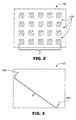
- FIGS. 2 and 3 are top views of aperture masks 10 that include deposition apertures separated by relatively large widths.
- FIG. 2 illustrates aperture mask 10B, which includes a pattern 12B of deposition apertures.
- Pattern 12B may define at least one dimension that is greater than approximately one centimeter, 25 centimeters, 100 centimeters, or even greater than approximately 500 centimeters. In other words, the distance X may be within those ranges.
- circuit elements separated by larger than conventional distances can be created using a deposition process. This feature may be advantageous, for example, in the fabrication of large area flat panel displays or detectors.
- aperture mask 10C of FIG. 3 includes at least two deposition apertures 36A and 36B.
- the two deposition apertures 36A and 36B can be separated by a distance X that is greater than approximately one centimeter, 25 centimeters, 100 centimeters, or even 500 centimeters.
- laser ablation techniques can facilitate the relatively large distance X because laser ablation systems can be easily designed to facilitate patterning over the large areas.
- laser ablation techniques can facilitate the creation of deposition apertures 36A and 36B to widths less than approximately 1000 microns, less than approximately 50 microns, less than approximately 20 microns, less than approximately 10 microns, or even less than approximately 5 microns.
- the deposition process would not necessarily require the aperture mask to be registered or aligned to a tolerance as small as the aperture widths. Still, the ability to deposit a circuit layer in a single deposition process with elements separated by these large distances can be highly advantageous for creating circuits that require large separation between two or more elements. Circuits for controlling or forming pixels of large electronic displays are one example.
- FIG. 4 is a top view of a mask set 40 that includes a number of aperture masks 10D-10I according to the invention for use in a deposition process.
- Mask set 40 may include any number of polymeric aperture masks, for example, depending on the circuit or circuit element to be created in the deposition process.
- Masks 10D-10I form a "set" in the sense that each mask may correspond to a particular layer or set of circuit elements within an integrated circuit.
- Each aperture mask 10 can be formed with a pattern of deposition apertures that define at least part of a layer of a circuit.
- a first aperture mask 10D may be formed with a first pattern of deposition apertures that define at least part of a first deposition layer of a circuit
- a second aperture mask 10E may be formed with a second pattern of deposition apertures that define at least part of a second deposition layer of the circuit.
- the mask set 40 may be used to create a wide variety of integrated circuits, such as integrated circuits which include both n-channel and p-channel thin film transistors (TFTs), such as a complimentary TFT element.
- TFTs thin film transistors
- organic or inorganic semiconductor materials may be used to create integrated circuits according to the invention. For some circuits, both organic and inorganic semiconductors may be used.
- first and second aperture masks 10D and 10E may define different layers of a circuit, and in other cases, first and second aperture masks 10D and 10E may define different portions of the same circuit layer.
- stitching techniques can be used in which first and second aperture masks 10D and 10E define different portions of the same circuit feature.
- two or more masks may be used in separate depositions to define a single circuit feature.
- Stitching techniques can be used, for example, to avoid relatively long deposition apertures, closed curves or any aperture pattern that would cause a portion of the aperture mask to be poorly supported, or not supported at all. In a first deposition, one mask forms part of a feature, and in a second deposition, another mask forms the remainder of the feature.
- Each aperture mask 10 in mask set 40 may comprise a polymer.
- laser ablation techniques can be used to form one or more deposition apertures having widths less than approximately 1000 microns, less than approximately 50 microns, less than approximately 20 microns, less than approximately 10 microns, or even less than approximately 5 microns.
- at least two deposition apertures in each aperture mask may be separated by a gap less than approximately 1000 microns, less than approximately 50 microns, less than approximately 20 microns, or less than approximately 10 microns. Apertures and gaps between apertures of these dimensions can reduce circuit size, and in some cases improve circuit performance.
- a dimension of the pattern of deposition apertures of aperture masks 10D-10I in mask set 40 may be in the ranges mentioned above to facilitate the creation of circuits having large dimensions.
- Polymeric aperture masks are useful with a wide variety of materials to be deposited. For example, organic or inorganic materials may be deposited through polymeric aperture masks. In one example, amorphous silicon may be deposited. Deposition of amorphous silicon typically requires high temperatures greater than approximately 200 degrees Celsius. Some embodiments of the polymeric aperture masks described herein may be able withstand these high temperatures, thus allowing amorphous silicon to be deposited through the polymeric mask to create integrated circuits or integrated circuit elements.
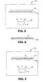
- FIG. 5 is a simplified block diagram of a deposition station that can use aperture masks in a deposition process according to the invention.
- deposition station 50 can be constructed to perform a vapor deposition process in which material is vaporized and deposited on a deposition substrate through an aperture mask.
- the deposited material may be semiconductor material such as an organic or inorganic semiconductor, dielectric material, or conductive material used to form a variety of elements within an integrated circuit. Other materials could also be used.
- Flexible aperture mask 10J is placed in proximity to a deposition substrate 52. In one example, flexible aperture mask 10J is sufficiently flexible such that it can be wound upon itself.
- flexible aperture mask 10J is sufficiently flexible such that it can be wound to a radius of curvature of less than approximately 1 centimeter without damage, or without forming a permanent bend.
- Deposition substrate 52 may comprise any of a variety of materials depending on the desired circuit to be created.
- deposition substrate 52 may comprise a flexible material, such as a flexible polymer.
- the desired circuit is a circuit of transistors for an electronic display
- deposition substrate 52 may comprise the backplane of the electronic display. Any deposition substrates such as glass substrates, silicon substrates, rigid plastic substrates, flexible plastic substrates, metal foils coated with insulating layers, or the like, could also be used.
- Deposition station 50 is typically a vacuum chamber. After flexible aperture mask 10J is placed in proximity to deposition substrate 52, material 56 is vaporized by deposition unit 54.
- deposition unit 54 may include a boat of material that is heated to vaporize the material.
- the vaporized material 56 deposits on deposition substrate 52 through the deposition apertures of flexible aperture mask 10J to define at least a portion of a circuit layer on deposition substrate 52.
- material 56 forms the pattern defined by flexible aperture mask 10J.
- Flexible aperture mask 10J may include deposition apertures and gaps that are sufficiently small to facilitate the creation of small circuit elements using the deposition process as described above. Additionally, the pattern of deposition apertures in flexible aperture mask 10J may have a large dimension as mentioned above.
- Other suitable deposition techniques include e-beam evaporation and various forms of sputtering and pulsed laser deposition.
- a sag problem may arise.
- flexible aperture mask 10J when flexible aperture mask 10J is placed in proximity to deposition substrate 52, flexible aperture mask 10J may sag as a result of the gravitational pull on flexible aperture mask 10J. This problem is most apparent when the aperture mask 10J is positioned underneath deposition substrate as shown in FIG. 5 .
- the sag problem compounds as flexible aperture mask 10J is made larger and larger.
- FIG. 5 illustrates the sag problem that results from gravitational pull on flexible aperture mask 10J.
- FIG. 6 is a cross-sectional side view of a flexible aperture mask 10K having a first side 61 that can removably adhere to a surface of a deposition substrate to facilitate intimate contact between the aperture mask and the deposition substrate during the deposition process.
- first side 61 of repositionable flexible aperture mask 10K may include a pressure sensitive adhesive. In that case, first side 61 can removably adhere to a deposition substrate via the pressure sensitive adhesive, and can then be removed after the deposition process.
- FIG. 7 is a block diagram of a deposition system 70 making use of flexible aperture mask 10K illustrated in FIG. 6 .
- the sag problem is overcome because first side 61 of flexible aperture mask 10K adheres to deposition substrate 52. Material 56 can then be vaporized by deposition unit 54 and deposited onto deposition substrate 52 according to the pattern defined in flexible aperture mask 10K.
- flexible aperture mask 10K may be removed and repositioned in order to achieve proper placement of flexible aperture mask 10K relative to deposition substrate 52 for the deposition process.
- aperture mask 10A may comprise both a polymer and magnetic material.
- the magnetic material may be coated or laminated on the polymer, or can be impregnated into the polymer.
- magnetic particles may be dispersed within a polymeric material used to form aperture mask 10A.
- a magnetic force can be applied within a deposition station to attract or repel the magnetic material in a manner that controls sag in aperture mask 10A.
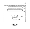
- a deposition station 80 may include magnetic structure 82.
- Aperture mask 10L may include a magnetic material.
- Magnetic structure 82 may attract aperture mask 10L so as to reduce, eliminate, or otherwise control sag in aperture mask 10L.
- magnetic structure 82 may be positioned such that sag is controlled by repelling the magnetic material within aperture mask 10L. In that case magnetic structure 82 would be positioned on the side of aperture mask 10L opposite deposition substrate 52.
- magnetic structure 82 can be realized by an array of permanent magnets or electromagnets.
- the aperture mask may comprise a polymer that is electrostatically coated or treated.
- magnetic structure 82 FIG. 8
- a charge may be applied to the aperture mask, the deposition substrate, or both to promote electrostatic attraction in a manner that promotes a sag reduction.
- Still another way to control sag is to stretch the aperture mask.
- a stretching unit can be implemented to stretch the aperture mask by an amount sufficient to reduce, eliminate, or otherwise control sag. As the mask is stretched tightly, sag is reduced. In that case, the aperture mask may need to have an acceptable coefficient of elasticity.
- FIG. 9a is a perspective view of an exemplary stretching unit for stretching aperture masks in accordance with the invention.
- Stretching unit 90 may include a relatively large deposition hole 92.
- An aperture mask can cover deposition hole 92 and a deposition substrate can be placed in proximity with the aperture mask.
- the aperture mask should allow elastic stretching without damage.
- the amount of stretching in one or more directions may be greater than approximately 0.1 percent, greater than approximately 0.5 percent, or even greater than approximately 1 percent.
- Material can be vaporized through deposition hole 92, and deposited on the deposition substrate according to the pattern defined in the aperture mask.
- Stretching unit 90 may include a number of stretching mechanisms 95A, 95B, 95C and 95D. Each stretching mechanism 95 may protrude up through a stretching mechanism hole 99 shown in FIG. 9b .
- each stretching mechanism 95 includes a top clamp portion 96 and a bottom clamp portion 97 that can clamp together upon an aperture mask. The aperture mask can then be stretched by moving stretching mechanisms 95 away from one another as they clamp the aperture mask. Stretching mechanisms 95 may move in directions along one or more axes. Stretching mechanisms 95 are illustrated as protruding from the top of stretching unit 90, but could alternatively protrude from the bottom of stretching unit. Particularly, if stretching unit 90 is used to control sag in an aperture mask, the stretching mechanisms would typically protrude from the bottom of stretching unit 90. Alternative methods of stretching the aperture mask could also be used either to control sag in the aperture mask or to properly align the aperture mask for the deposition process. By stretching the aperture mask, misalignment due to thermal expansion can be greatly minimized.
- laser ablation techniques can be used to create the pattern of deposition apertures in a polymeric aperture mask, for example, by ablating a polymeric film to define the pattern of deposition apertures.
- the pattern may define first and second pattern elements separated by more than approximately 25 centimeters.
- FIG. 10 is a block diagram of a laser ablation system that can be used to ablate aperture masks in accordance with the invention.
- Laser ablation techniques are advantageous because they can achieve relatively small deposition apertures and can also define patterns on a single aperture mask that are much larger than conventional patterns.
- laser ablation techniques may facilitate the creation of aperture masks at significantly lower cost than other conventional techniques commonly used to create metal or silicon aperture masks.
- laser ablation system 100 may be a projection laser ablation system utilizing a patterned ablation mask, although a shadow mask ablation system or phase mask ablation system could be used. Spot-writing a single laser spot can also be used to "write" the desired pattern of apertures.
- Projection imaging laser ablation is a technique for producing very small parts or very small structures on a surface of an object being ablated, the structures having sizes on the order of between one micron to several millimeters, whereby light is passed through a patterned ablation mask and the pattern is imaged onto the object being ablated. Material is removed from the ablation substrate in the areas that receive light.
- UV ultraviolet
- the illumination provided by the laser can be any kind of light, such as infrared or visible light.
- the invention may be applied using light sources that are not lasers.
- Laser 101 may be a KrF excimer laser emitting a beam with a short wavelength of light of approximately 248 nm.
- any type of excimer laser may be used, such as F 2 , ArF, KrCl, or XeCl type excimer lasers.
- An excimer laser is particularly useful in creating small deposition apertures because an excimer laser can resolve smaller features and cause less collateral damage than lasers such as CO 2 lasers, which emit beams with a wavelength of approximately 10,600 nm.
- excimer lasers can be used with most polymers that are transparent to light from lasers typically used for processing metals, such as Neodymium doped Yttrium Aluminum Garnet (Nd:YAG) lasers.
- Nd:YAG Neodymium doped Yttrium Aluminum Garnet
- Excimer lasers are also advantageous because at UV wavelengths, most materials, such as polymers, have high absorption. Therefore, more energy is concentrated in a shallower depth and the excimer laser provides cleaner cutting.
- Excimer lasers are pulsed lasers, the pulses ranging from 5-300 nanoseconds.
- Laser 101 may also be a tripled or quadrupled Nd:YAG laser or any laser having pulses in the femtosecond range.
- Ablation mask 103 may be a patterned mask having pattern 102 manufactured using standard semiconductor lithography mask techniques.
- the patterned portions of ablation mask 103 are opaque to UV light, while a support substrate of ablation mask are transparent to UV light.
- the patterned portions comprise aluminum while the support substrate for ablation mask 103 is fused silica (SiO 2 ).
- Fused silica is a useful support material because it is one of the few materials that is transparent to mid and far UV wavelengths. Calcium fluoride may be used as the support substrate as an alternative to SiO 2 .
- Aluminum is useful as a patterning material because it reflects mid-UV light.
- a patterned dielectric stack is one alternative to aluminum.
- Imaging lens 104 may be a single lens or an entire optical system consisting of a number of lenses and other optical components. Imaging lens 104 projects an image of the ablation mask, more specifically, an image of the pattern of light passing through the ablation mask onto surface of object to be ablated 105.
- the object to be ablated is a polymeric film 106, possibly including a material 107 formed on the back side of the polymeric film.
- Some suitable polymeric films may comprise polyimide, polyester, polystyrene, polymethyl methacrylate, polycarbonate, or combinations thereof.
- FIG. 11 illustrates a useful structure that can form the object to be ablated 105.
- FIG. 11 illustrates an object to be ablated 105 that includes a polymer film 106 with a material 107 formed on the back side, i.e. a side opposite the side incident to the laser in system 100 ( FIG. 10 ).
- Material 107 provides an etch stop for the ablation process which can avoid air entrapment under polymer film 106, and can be a stabilizing carrier.
- material 107 may comprise a metal such as copper.
- material 107 is etched from polymer film 106, to form a polymeric aperture mask. Alternatively, in some embodiments, material 107 may be peeled away.
- Objects 105 may be created by forming a copper layer on a polymer film, or by forming the polymer film on a copper layer. In some cases, objects 105 may simply be purchased in a preformed configuration.
- table 109 supports and positions the object to be ablated 105.
- object to be ablated 105 can be fixed into position on table 109, such as by vacuum chuck 108, static electricity, mechanical fasteners or a weight.
- Table 109 can position the object to be ablated 105 by moving the object 105 on the x, y and z axes as well as rotationally, such as along the z axis.
- Table 109 can move object 105 in steps down to approximately 5 nm, and more typically, approximately 100 nm, reproducible to an accuracy of approximately 500 nm.
- Computer control of table 109 can allow preprogramming of the movement of table 109 as well as possible synchronization of table movement with the emission of light from laser 101.
- the table may also be manually controlled, such as with a joystick connected to a computer.
- the invention may control the ablation so as to achieve an acceptable wall angle.
- a straight wall angle i.e., a zero (0) degree wall angle, corresponds to a deposition aperture having walls that are perpendicular to the surface of the polymer film.
- a negative wall angle can be achieved, wherein the hole assumes a larger and larger diameter as the laser ablates through the polymer material.
- a number of factors can affect the wall angle. Accordingly these factors can be controlled to achieve an acceptable, or a desired wall angle.
- the power density of the laser radiation at the substrate and the numerical aperture of the imaging system can be controlled to achieve an acceptable wall angle. Additional factors that may be controlled include the pulse length of the laser, and the ablation threshold of the object or material being ablated.
- the aperture wall angle should be near zero to allow the closest possible spacing between apertures.
- a wall angle greater than zero is desirable to minimize parallax in regions of the mask where the deposition flux impinges the deposition substrate at an angle substantially different from perpendicular.
- FIGS. 12 and 13 are cross-sectional views of exemplary thin film transistors that can be created according to the invention.
- thin film transistors 130 and 140 can be created without using any etching or lithography techniques. Instead, thin film transistors 130 and 140 can be created solely using aperture mask deposition techniques as described herein. Alternatively, one or more bottom layers may be etched or lithographically patterned, with at least two of the top most layers being formed by the aperture mask deposition techniques described herein. Importantly, the deposition techniques achieve sufficiently small circuit features in the thin film transistors.
- the invention can facilitate the creation of thin film transistors in which the organic semiconductor is not the top-most layer of the circuit.
- electrode patterns may be formed over the organic semiconductor material. Electrode patterns formed over the organic semiconductor often result in thin film transistors with improved device characteristics. This advantage of aperture mask 10 can be exploited while at the same time achieving acceptable sizes of the circuit elements.
- Thin film transistors are commonly implemented in a variety of different circuits, including for example, RFID circuits, electronic memory, and other low cost circuits.
- thin film transistors can be used as control elements for liquid crystal display pixels, or other flat panel display pixels, including organic light emitting diodes. Many other applications for thin film transistors also exist.
- thin film transistor 130 is formed on a deposition substrate 131.
- Thin film transistor 130 represents one embodiment of a transistor in which all of the layers are deposited using an aperture mask and none of the layers are formed using etching or lithography techniques.
- the aperture mask deposition techniques described herein can enable the creation of thin film transistor 130 in which a distance between electrodes 135 and 136 is less than approximately 1000 microns, less than approximately 50 microns, less than approximately 20 microns, or even less than approximately 10 microns, while at the same time avoiding conventional etching or lithography processes.
- thin film transistor 130 includes a first deposited conductive layer 132 formed over deposition substrate 131.
- a deposited dielectric layer 133 is formed over first conductive layer 132.
- a second deposited conductive layer 134 defining source electrode 135 and drain electrode 136 is formed over deposited dielectric layer 133.
- a deposited active layer 137 such as a deposited semiconductor layer, or a deposited organic semiconductor layer is formed over second deposited conductive layer 134.
- Deposition techniques using mask set 40 represent one exemplary method of creating thin film transistor 130.
- each layer of thin film transistor 130 may be defined by one or more deposition apertures in deposition aperture masks 10D-10I that form mask set 40.
- one or more of the layers of the thin film transistor may be created using a number of aperture masks and stitching techniques, as mentioned above.
- one or more features of thin film transistor 130 can be made with a width less than approximately 1000 microns, less than approximately 50 microns less than approximately 20 microns, less than approximately 10 microns, or even less than approximately 5 microns.
- other features such as the distance between source electrode 135 and drain electrode 136 can be made less than approximately 1000 microns, less than approximately 50 microns less than approximately 20 microns or even less than approximately 10 microns.
- a single mask may be used to deposit second conductive layer 134, with each of the two electrodes 135, 136 being defined by deposition apertures separated by a sufficiently small gap.
- a circuit comprising two or more transistors can be formed by an aperture mask having two deposition apertures separated by a large distance, as illustrated in FIGS. 2 and 3 .
- FIG. 13 illustrates another embodiment of a thin film transistor 140.
- thin film transistor 140 includes a first deposited conductive layer 142 formed over deposition substrate 141.
- a deposited dielectric layer 143 is formed over first conductive layer 142.
- a deposited active layer 144 such as a deposited semiconductor layer, or a deposited organic semiconductor layer is formed over deposited dielectric layer 143.
- a second deposited conductive layer 145 defining source electrode 146 and drain electrode 147 is formed over deposited active layer 144.
- one or more features of thin film transistor 140 can have widths on the order of those discussed herein.
- a gap in an aperture mask to be sufficiently small, the distance between source electrode 146 and drain electrode 147 can be on the order of the gaps discussed herein.
- a single mask may be used to deposit second conductive layer 145, with each of the two electrodes 146, 147 being defined by deposition apertures separated by a sufficiently small gap. In this manner, the size of thin film transistor 140 can be reduced, and the performance of thin film transistor 140 can be improved.
- thin film transistors implementing organic semiconductors may take the form of FIG. 12 because organic semiconductors typically cannot be etched or lithographically patterned without damaging or degrading the performance of the organic semiconductor material. For instance, morphological changes can occur in an organic semiconductor layer upon exposure to processing solvents. For this reason, fabrication techniques in which the organic semiconductor is deposited as a top layer are commonly used.
- the invention facilitates the configuration of FIG. 13 , even if active layer 144 is an organic semiconductor layer.
- the configuration of FIG. 13 can promote improved growth of the organic semiconductor layer by allowing the organic semiconductor layer to be deposited over the relatively flat surface of dielectric layer 143, as opposed to being deposited over the non-continuous second conductive layer 134 as illustrated in FIG. 12 .
- the configuration of FIG. 13 may be desirable. In some embodiments, all of the layers may be deposited as described above. Also, the configuration of FIG.
- circuits having two or more transistors separated by a large distance can also be created, for example, using masks like those illustrated in FIGS. 2 and 3 .
- an aperture mask may be used to deposit a patterned active layer which may enhance device performance, particularly in cases where the active layer comprises an organic semiconductor, for which conventional patterning processes are incompatible.
- the semiconductor may be amorphous (e.g., amorphous silicon) or polycrystalline (e.g., pentacene).
- One particular technique for creating a circuit or a circuit element includes positioning an aperture mask.
- the mask may be positioned in proximity to a deposition substrate.
- the mask may be placed in intimate contact with the deposition substrate, and in other cases, it can be advantageous to maintain a small gap between the deposition substrate and the aperture mask.
- the aperture mask can then be stretched. Stretching the aperture mask can achieve one or more of a number of different goals. For example, stretching the aperture mask can reduce sag in the mask. Alternatively or additionally, stretching the aperture mask can align the mask for the deposition process. After stretching the aperture mask, material can be deposited through the aperture mask onto the deposition substrate to form a layer on the deposition substrate.
- the layer may comprise a layer in an integrated circuit, including, for example, a layer in a thin film transistor, a diode, or a radio frequency identification circuit.
- the diode may be a light emitting diode, including an organic light emitting diode.
- Another technique of creating a circuit or a circuit element includes positioning an aperture mask and controlling sag in the aperture mask.
- the aperture mask may be positioned in proximity to a deposition substrate. Again, in some cases, the mask may be placed in intimate contact with the deposition substrate, and in other cases, it can be advantageous to maintain a small gap between the deposition substrate and the aperture mask.
- Controlling sag can be performed in a number of ways including using magnetic force, electrostatics, stretching techniques, or adhering the mask to the deposition substrate such as with a pressure sensitive adhesive.
- a material layer is formed on a first side of a polymeric film.
- the polymeric film may be formed on the material.
- the material may comprise a metal such as copper.
- the polymeric film can be ablated from a side opposite the material layer, and the material layer can be removed. For example, if the material layer is metallic, it can be removed by etching or peeling away the metal. In this manner, a polymeric aperture mask can be fabricated.
- a repositionable polymeric aperture mask can also be used as a pattern in an etching process, including a process to etch at least one layer of a thin film transistor. Then, the same repositionable polymeric aperture mask can be reused as a pattern in another etching process. This technique can simplify a large scale repeated etching process, and also reduce the cost of implementing the same etching process a number of times.
- an aperture mask in another technique, if an aperture mask is made flexible, it can facilitate the creation of integrated circuits on a non-planar deposition substrate.
- a flexible and repositionable aperture mask can be positioned over the non-planar deposition substrate. Then, a layer or a portion of a layer of an integrated circuit can be formed on the non-planar deposition substrate.
- the layer of the integrated circuit may comprise at least a portion of a thin film transistor.
- the aperture masks described herein can be particularly useful when the deposition process requires intimate contact between the aperture mask and the deposition substrate. In that case, flexible polymeric aperture masks can conform to the surface of the non-planar substrate to facilitate the intimate contact.
- a pattern is ablated in a polymeric film to create a free-standing aperture mask.
- ablation can be controlled to create an acceptable wall-angle.
- factors that can affect the wall angle are listed above, such as the power density of the laser, the numerical aperture of the imaging system, the pulse length of the laser, and the ablation threshold of the object or material being ablated. One or more of these factors can be controlled as desired to ensure that an acceptable wall angle is achieved.
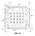
- FIG. 14 is a top view of an aperture mask being stretched in accordance with the invention.
- Aperture mask 150 comprises a mask substrate formed with pattern 151 as described above.
- aperture mask 150 may include extension portions 152A-152D of the mask substrate that can be used to stretch aperture mask 150 and to improve uniformity of the stretching of pattern 151 without distortion.
- Each extension portion 152 may include a set of distortion minimizing features, such as slits (only distortion minimizing features 154 labeled), which may be located near the edge of pattern 151.
- the distortion minimizing features 154 can facilitate more precise stretching of aperture mask 150 by reducing distortion of pattern 151 during stretching.
- Various configurations of distortion minimizing features include slits in the mask substrate, holes in the mask substrate, perforations in the mask substrate, reduced thickness areas in the mask substrate, and the like.
- Clamps 156A-156D can be mounted on extension portions 152 of aperture mask 150.
- Each clamp 156 may be attached to one or more wires, strings, or the like.
- each clamp 156 includes two strings, thus providing a total of eight degrees of freedom during stretching.
- the strings can be attached to micrometers mounted on an alignment backing structure. Tension in the strings can be adjusted to provide positioning and a desired amount of stretching of aperture mask 150. In this manner, mask 150 can be aligned with deposition substrate 160.
- organic integrated circuits were fabricated using four vacuum deposition steps, and four stretched polymer aperture masks. The process used no photolithography and no wet processing.
- All four polymer aperture masks were made with the same technique, which involved laser ablation of apertures in 25 micron thick sheets of polyimide with copper backing that was approximately 18 microns thick. After the laser ablation, the copper was removed in an acid etchant, 10 HNO 3 : 1 HCl, and the mask was rinsed and cleaned. In each mask, the patterned region was approximately 4.5 cm x 4.5 cm.
- the aperture masks including: (1) gate metal, (2) insulator (dielectric), (3) semiconductor, and (4) source/drain metal. Interconnections between circuit components were made by stitching traces in the gate and source/drain layers. In this example, the integrated circuit was designed with minimum line widths of 15 microns.
- Each of the masks was mounted between four clamps as shown in FIG. 14 . Stretching and alignment were accomplished using the eight strings that were attached to the ends of clamps 156. Each of the strings was connected to a micrometer mounted on an alignment structure. Each clamp allowed tension to be applied uniformly along one side of the mask. By using at least five (in this case eight) or more degrees of freedom, the elasticity of the mask was used to achieve excellent alignment over the entire patterned area.
- distortion minimizing features 154 in the form of slits, were cut through the mask on each side between the patterned region and the clamp.
- the slits ran parallel to the direction of tension applied by the adjacent clamp 156, and in this example were spaced approximately 2.5 mm apart from each other, although the invention is not limited in that respect.
- the slits, located near the patterned region, allowed the patterned region of the mask to stretch in the direction perpendicular to the slits with very little constraint by clamps 156. In other words, the patterned region was allowed to stretch uniformly in all directions.
- a 50 mm x 75 mm x 0.7 mm float glass deposition substrate was placed in contact with the first mask with minimal downward force so as to minimize stiction and friction.
- the first mask was stretched about 0.5% in both directions.
- the mask, stretching mechanisms and substrate were placed in a vacuum system and the first layer, 50 nm of Pd, was deposited by ion beam sputtering. Electron beam evaporation could also be used.
- the assembly was removed and the first mask was replaced with the second mask.
- the second mask was stretched and aligned to features of the first layer on the substrate.
- the assembly was placed in a vacuum system and the second layer, 200 nm of Al 2 O 3 , was deposited by electron-beam evaporation. Sputtering could also be used.
- the assembly was again removed and the second mask was replaced with the third mask.
- the third mask was stretched and aligned to features of the first layer on the substrate.
- the assembly was placed in a vacuum system and the third layer, 50 nm of pentacene, was deposited by thermal evaporation.
- the assembly was removed again and the third mask was replaced with the fourth mask.
- the fourth mask was stretched and aligned to features of the first layer on the substrate.
- the assembly was placed in a vacuum system and the fourth layer, 150 nm of Au, was deposited by thermal evaporation. Sputtering or electron beam evaporation could also be used.
- the driving circuitry for the Organic Light Emitting Diode (OLED) subpixels is provided on the substrate, and can be either active matrix or passive matrix, both of which are known in the art.
- the driving circuitry includes electrodes (for example, indium tin oxide anodes) for the OLED subpixels.
- the substrate may also include spacers of, for example, photoresist of height 0.1 to 10 microns which hold the aperture mask away from the substrate surface to prevent damage to materials on the substrate when the mask is moved.
- the mask pattern is a series of rectangular apertures in a rectangular array, formed by laser ablation.
- the apertures are, for example, 100 microns square, and are spaced 250 microns center-to-center in both dimensions.
- the OLED subpixels are made by optionally first depositing a buffer layer, such as polythiophene (e.g., Baytron P from Bayer) over all of the electrodes by spin coating. Alternatively, buffer layers may be vacuum deposited. Next, a hole transport layer, such as 40 nm. NPD (N,N'-Di(naphthalen-1-yl)-N,N'diphenylbenzidine) is vacuum evaporated over the buffer layer.
- a buffer layer such as polythiophene (e.g., Baytron P from Bayer)
- buffer layers may be vacuum deposited.
- a hole transport layer such as 40 nm.
- NPD N,N'-Di(naphthalen-1-yl)-N,N'diphenyl
- the aperture mask is stretched as in the previous example and aligned to the electrodes for the red subpixels.
- the red electroluminescent layer is then deposited through the aperture mask.
- This layer may be, for example, 10 nm of a mixture of 10 weight percent PtOEP (platinum octaethylporphyrin) in CBP (4,4'-Bis(carbazol-9-yl)biphenyl), formed by simultaneously evaporation PtOEP and CBP from two sources.
- the aperture mask is then moved, possibly while still in the vacuum, to be aligned with the electrodes for the green subpixels.
- the green electroluminescent layer is then vacuum deposited through the aperture mask.
- This layer may be, for example, 10 nm of a mixture of 10 weight percent Ir(ppy) 3 (tris(2-phenylpyridine)iridium) in CBP.
- the mask is then moved, possibly while still in the vacuum, to be aligned with the electrodes for the blue subpixels.
- the blue electroluminescent layer is then vacuum deposited through the aperture mask.
- This layer may be, for example, 10 nm CBP.
- a blue dopant such as perylene (10 weight percent in CBP), may be used.
- a cathode is deposited over all of the subpixels.
- the cathode may be, for example, 0.5 nm of LiF followed by 200 nm of Al.
- the cathodes In the case of a passive matrix display, the cathodes must be patterned into rows, typically by using another shadow mask.
Applications Claiming Priority (2)
| Application Number | Priority Date | Filing Date | Title |
|---|---|---|---|
| US10/076,174 US6897164B2 (en) | 2002-02-14 | 2002-02-14 | Aperture masks for circuit fabrication |
| EP03707482A EP1481111A2 (de) | 2002-02-14 | 2003-01-21 | Lochmasken zur herstellung von schaltungen |
Related Parent Applications (1)
| Application Number | Title | Priority Date | Filing Date |
|---|---|---|---|
| EP03707482.0 Division | 2003-01-21 |
Publications (2)
| Publication Number | Publication Date |
|---|---|
| EP2159303A2 true EP2159303A2 (de) | 2010-03-03 |
| EP2159303A3 EP2159303A3 (de) | 2010-09-29 |
Family
ID=27660193
Family Applications (2)
| Application Number | Title | Priority Date | Filing Date |
|---|---|---|---|
| EP03707482A Withdrawn EP1481111A2 (de) | 2002-02-14 | 2003-01-21 | Lochmasken zur herstellung von schaltungen |
| EP09175050A Withdrawn EP2159303A3 (de) | 2002-02-14 | 2003-01-21 | Lochmasken zur Herstellung von Schaltungen |
Family Applications Before (1)
| Application Number | Title | Priority Date | Filing Date |
|---|---|---|---|
| EP03707482A Withdrawn EP1481111A2 (de) | 2002-02-14 | 2003-01-21 | Lochmasken zur herstellung von schaltungen |
Country Status (7)
| Country | Link |
|---|---|
| US (3) | US6897164B2 (de) |
| EP (2) | EP1481111A2 (de) |
| JP (1) | JP4490105B2 (de) |
| KR (1) | KR20040091038A (de) |
| CN (1) | CN100519829C (de) |
| AU (1) | AU2003209328A1 (de) |
| WO (1) | WO2003069015A2 (de) |
Families Citing this family (162)
| Publication number | Priority date | Publication date | Assignee | Title |
|---|---|---|---|---|
| AU2001250958A1 (en) | 2000-03-24 | 2001-10-08 | Cymbet Corporation | Continuous processing of thin-film batteries and like devices |
| CA2426641C (en) * | 2001-08-24 | 2010-10-26 | Dai Nippon Printing Co., Ltd. | Multi-face forming mask device for vacuum deposition |
| US6821348B2 (en) * | 2002-02-14 | 2004-11-23 | 3M Innovative Properties Company | In-line deposition processes for circuit fabrication |
| US20030151118A1 (en) * | 2002-02-14 | 2003-08-14 | 3M Innovative Properties Company | Aperture masks for circuit fabrication |
| US6897164B2 (en) * | 2002-02-14 | 2005-05-24 | 3M Innovative Properties Company | Aperture masks for circuit fabrication |
| SG113448A1 (en) * | 2002-02-25 | 2005-08-29 | Semiconductor Energy Lab | Fabrication system and a fabrication method of a light emitting device |
| US6727125B2 (en) * | 2002-04-17 | 2004-04-27 | Sharp Laboratories Of America, Inc. | Multi-pattern shadow mask system and method for laser annealing |
| US6667215B2 (en) | 2002-05-02 | 2003-12-23 | 3M Innovative Properties | Method of making transistors |
| KR100480705B1 (ko) * | 2002-07-03 | 2005-04-06 | 엘지전자 주식회사 | 유기 el 소자 제작용 새도우 마스크 및 그 제조 방법 |
| JP2004183044A (ja) * | 2002-12-03 | 2004-07-02 | Seiko Epson Corp | マスク蒸着方法及び装置、マスク及びマスクの製造方法、表示パネル製造装置、表示パネル並びに電子機器 |
| JP2004186395A (ja) * | 2002-12-03 | 2004-07-02 | Fujitsu Ltd | セラミック基板の製造方法 |
| US7088145B2 (en) * | 2002-12-23 | 2006-08-08 | 3M Innovative Properties Company | AC powered logic circuitry |
| US7603144B2 (en) * | 2003-01-02 | 2009-10-13 | Cymbet Corporation | Active wireless tagging system on peel and stick substrate |
| US6906436B2 (en) * | 2003-01-02 | 2005-06-14 | Cymbet Corporation | Solid state activity-activated battery device and method |
| US7294209B2 (en) * | 2003-01-02 | 2007-11-13 | Cymbet Corporation | Apparatus and method for depositing material onto a substrate using a roll-to-roll mask |
| US7417782B2 (en) | 2005-02-23 | 2008-08-26 | Pixtronix, Incorporated | Methods and apparatus for spatial light modulation |
| US6680521B1 (en) * | 2003-04-09 | 2004-01-20 | Newport Fab, Llc | High density composite MIM capacitor with reduced voltage dependence in semiconductor dies |
| US7098525B2 (en) | 2003-05-08 | 2006-08-29 | 3M Innovative Properties Company | Organic polymers, electronic devices, and methods |
| US7279777B2 (en) * | 2003-05-08 | 2007-10-09 | 3M Innovative Properties Company | Organic polymers, laminates, and capacitors |
| US7109519B2 (en) * | 2003-07-15 | 2006-09-19 | 3M Innovative Properties Company | Bis(2-acenyl)acetylene semiconductors |
| US20070178710A1 (en) * | 2003-08-18 | 2007-08-02 | 3M Innovative Properties Company | Method for sealing thin film transistors |
| US20050079418A1 (en) * | 2003-10-14 | 2005-04-14 | 3M Innovative Properties Company | In-line deposition processes for thin film battery fabrication |
| US7153180B2 (en) * | 2003-11-13 | 2006-12-26 | Eastman Kodak Company | Continuous manufacture of flat panel light emitting devices |
| US20050130422A1 (en) * | 2003-12-12 | 2005-06-16 | 3M Innovative Properties Company | Method for patterning films |
| US7078937B2 (en) | 2003-12-17 | 2006-07-18 | 3M Innovative Properties Company | Logic circuitry powered by partially rectified ac waveform |
| JP2007518246A (ja) * | 2004-01-06 | 2007-07-05 | シンベット コーポーレーション | 境界を有する1若しくはそれ以上の層を備える層状のバリア構造及び該バリア構造の製造方法 |
| US7223674B2 (en) * | 2004-05-06 | 2007-05-29 | Micron Technology, Inc. | Methods for forming backside alignment markers useable in semiconductor lithography |
| US7399668B2 (en) * | 2004-09-30 | 2008-07-15 | 3M Innovative Properties Company | Method for making electronic devices having a dielectric layer surface treatment |
| US20060086321A1 (en) * | 2004-10-22 | 2006-04-27 | Advantech Global, Ltd | Substrate-to-mask alignment and securing system with temperature control for use in an automated shadow mask vacuum deposition process |
| US7298084B2 (en) * | 2004-11-02 | 2007-11-20 | 3M Innovative Properties Company | Methods and displays utilizing integrated zinc oxide row and column drivers in conjunction with organic light emitting diodes |
| KR101074389B1 (ko) * | 2004-11-05 | 2011-10-17 | 엘지디스플레이 주식회사 | 박막 식각 방법 및 이를 이용한 액정표시장치의 제조방법 |
| US20060107525A1 (en) * | 2004-11-22 | 2006-05-25 | Hamburgen William R | Method and system for creating alignment holes in a multilayer structure |
| US20060128165A1 (en) * | 2004-12-13 | 2006-06-15 | 3M Innovative Properties Company | Method for patterning surface modification |
| GB0427563D0 (en) * | 2004-12-16 | 2005-01-19 | Plastic Logic Ltd | A method of semiconductor patterning |
| US8482496B2 (en) | 2006-01-06 | 2013-07-09 | Pixtronix, Inc. | Circuits for controlling MEMS display apparatus on a transparent substrate |
| US8519945B2 (en) | 2006-01-06 | 2013-08-27 | Pixtronix, Inc. | Circuits for controlling display apparatus |
| US7742016B2 (en) | 2005-02-23 | 2010-06-22 | Pixtronix, Incorporated | Display methods and apparatus |
| US8310442B2 (en) | 2005-02-23 | 2012-11-13 | Pixtronix, Inc. | Circuits for controlling display apparatus |
| US7746529B2 (en) | 2005-02-23 | 2010-06-29 | Pixtronix, Inc. | MEMS display apparatus |
| US8159428B2 (en) | 2005-02-23 | 2012-04-17 | Pixtronix, Inc. | Display methods and apparatus |
| US9261694B2 (en) | 2005-02-23 | 2016-02-16 | Pixtronix, Inc. | Display apparatus and methods for manufacture thereof |
| US9082353B2 (en) | 2010-01-05 | 2015-07-14 | Pixtronix, Inc. | Circuits for controlling display apparatus |
| US9229222B2 (en) | 2005-02-23 | 2016-01-05 | Pixtronix, Inc. | Alignment methods in fluid-filled MEMS displays |
| US20070205969A1 (en) | 2005-02-23 | 2007-09-06 | Pixtronix, Incorporated | Direct-view MEMS display devices and methods for generating images thereon |
| US7675665B2 (en) | 2005-02-23 | 2010-03-09 | Pixtronix, Incorporated | Methods and apparatus for actuating displays |
| US9158106B2 (en) | 2005-02-23 | 2015-10-13 | Pixtronix, Inc. | Display methods and apparatus |
| US7755582B2 (en) | 2005-02-23 | 2010-07-13 | Pixtronix, Incorporated | Display methods and apparatus |
| US7999994B2 (en) | 2005-02-23 | 2011-08-16 | Pixtronix, Inc. | Display apparatus and methods for manufacture thereof |
| US7271945B2 (en) * | 2005-02-23 | 2007-09-18 | Pixtronix, Inc. | Methods and apparatus for actuating displays |
| US7211679B2 (en) * | 2005-03-09 | 2007-05-01 | 3M Innovative Properties Company | Perfluoroether acyl oligothiophene compounds |
| US7151276B2 (en) * | 2005-03-09 | 2006-12-19 | 3M Innovative Properties Company | Semiconductors containing perfluoroether acyl oligothiophene compounds |
| US7645478B2 (en) * | 2005-03-31 | 2010-01-12 | 3M Innovative Properties Company | Methods of making displays |
| US7667929B2 (en) * | 2005-04-04 | 2010-02-23 | Hitachi Global Storage Technologies Netherlands B.V. | Apparatus, method and system for fabricating a patterned media imprint master |
| ITRM20050258A1 (it) * | 2005-05-25 | 2006-11-26 | Istituto Naz Fisica Nucleare | Procedimento di produzione di gioielli, utilizzante tecniche di deposizione pvd e di mascheratura di film metallico o minerale su substrati metallici, minerali, plastici e autoadesivi. |
| US7507618B2 (en) * | 2005-06-27 | 2009-03-24 | 3M Innovative Properties Company | Method for making electronic devices using metal oxide nanoparticles |
| JP2009501280A (ja) | 2005-07-12 | 2009-01-15 | スリーエム イノベイティブ プロパティズ カンパニー | 基材上に材料模様を連続的に付着させるための装置及び方法 |
| US20070012244A1 (en) * | 2005-07-15 | 2007-01-18 | Cymbet Corporation | Apparatus and method for making thin-film batteries with soft and hard electrolyte layers |
| WO2007011900A1 (en) * | 2005-07-15 | 2007-01-25 | Cymbet Corporation | Thin-film batteries with soft and hard electrolyte layers and method |
| US7776478B2 (en) * | 2005-07-15 | 2010-08-17 | Cymbet Corporation | Thin-film batteries with polymer and LiPON electrolyte layers and method |
| US7319153B2 (en) * | 2005-07-29 | 2008-01-15 | 3M Innovative Properties Company | 6,13-Bis(thienyl)pentacene compounds |
| US7615501B2 (en) * | 2005-08-11 | 2009-11-10 | 3M Innovative Properties Company | Method for making a thin film layer |
| US7544754B2 (en) | 2005-09-30 | 2009-06-09 | 3M Innovative Properties Company | Crosslinked polymers with amine binding groups |
| US7544756B2 (en) * | 2005-09-30 | 2009-06-09 | 3M Innovative Properties Company | Crosslinked polymers with amine binding groups |
| US7544755B2 (en) * | 2005-09-30 | 2009-06-09 | 3M Innovative Properties Company | Crosslinked polymers with amine binding groups |
| KR100652442B1 (ko) * | 2005-11-09 | 2006-12-01 | 삼성전자주식회사 | 반도체 칩 및 그 제조 방법 |
| US20070137568A1 (en) * | 2005-12-16 | 2007-06-21 | Schreiber Brian E | Reciprocating aperture mask system and method |
| US7763114B2 (en) * | 2005-12-28 | 2010-07-27 | 3M Innovative Properties Company | Rotatable aperture mask assembly and deposition system |
| US8526096B2 (en) | 2006-02-23 | 2013-09-03 | Pixtronix, Inc. | Mechanical light modulators with stressed beams |
| US7608679B2 (en) * | 2006-03-31 | 2009-10-27 | 3M Innovative Properties Company | Acene-thiophene copolymers |
| US7667230B2 (en) * | 2006-03-31 | 2010-02-23 | 3M Innovative Properties Company | Electronic devices containing acene-thiophene copolymers |
| US7666968B2 (en) * | 2006-04-21 | 2010-02-23 | 3M Innovative Properties Company | Acene-thiophene copolymers with silethynly groups |
| US7495251B2 (en) * | 2006-04-21 | 2009-02-24 | 3M Innovative Properties Company | Electronic devices containing acene-thiophene copolymers with silylethynyl groups |
| DE102006024175B3 (de) * | 2006-05-23 | 2007-09-27 | Touchtek Corporation, Chunan | Verfahren zum Herstellen von primären Mehrschichtelektroden |
| US7876489B2 (en) | 2006-06-05 | 2011-01-25 | Pixtronix, Inc. | Display apparatus with optical cavities |
| US20080011225A1 (en) * | 2006-07-11 | 2008-01-17 | Mcclure Donald J | Apparatus and methods for continuously depositing a pattern of material onto a substrate |
| DE102006042617B4 (de) * | 2006-09-05 | 2010-04-08 | Q-Cells Se | Verfahren zur Erzeugung von lokalen Kontakten |
| US20080094853A1 (en) | 2006-10-20 | 2008-04-24 | Pixtronix, Inc. | Light guides and backlight systems incorporating light redirectors at varying densities |
| KR100836471B1 (ko) * | 2006-10-27 | 2008-06-09 | 삼성에스디아이 주식회사 | 마스크 및 이를 이용한 증착 장치 |
| US8906703B2 (en) | 2006-12-21 | 2014-12-09 | 3M Innovative Properties Company | Surface-bound fluorinated esters for amine capture |
| US8357540B2 (en) * | 2006-12-21 | 2013-01-22 | 3M Innovative Properties Company | Polymeric substrates with fluoroalkoxycarbonyl groups for amine capture |
| US20080171422A1 (en) * | 2007-01-11 | 2008-07-17 | Tokie Jeffrey H | Apparatus and methods for fabrication of thin film electronic devices and circuits |
| US7852546B2 (en) | 2007-10-19 | 2010-12-14 | Pixtronix, Inc. | Spacers for maintaining display apparatus alignment |
| US9176318B2 (en) | 2007-05-18 | 2015-11-03 | Pixtronix, Inc. | Methods for manufacturing fluid-filled MEMS displays |
| JP5473609B2 (ja) * | 2007-02-13 | 2014-04-16 | スリーエム イノベイティブ プロパティズ カンパニー | レンズを有するledデバイス及びその作製方法 |
| US9944031B2 (en) | 2007-02-13 | 2018-04-17 | 3M Innovative Properties Company | Molded optical articles and methods of making same |
| JP5132213B2 (ja) * | 2007-07-18 | 2013-01-30 | 富士フイルム株式会社 | 蒸着装置及び蒸着方法並びにその方法を用いてパターン形成した層を有する電子素子及び有機エレクトロルミネッセンス素子 |
| TWI466298B (zh) * | 2007-09-11 | 2014-12-21 | Au Optronics Corp | 畫素結構的製作方法 |
| KR100947442B1 (ko) * | 2007-11-20 | 2010-03-12 | 삼성모바일디스플레이주식회사 | 수직 증착형 마스크 제조장치 및 이를 이용한 수직 증착형마스크의 제조방법 |
| US8248560B2 (en) | 2008-04-18 | 2012-08-21 | Pixtronix, Inc. | Light guides and backlight systems incorporating prismatic structures and light redirectors |
| US8169679B2 (en) | 2008-10-27 | 2012-05-01 | Pixtronix, Inc. | MEMS anchors |
| TWI475124B (zh) | 2009-05-22 | 2015-03-01 | Samsung Display Co Ltd | 薄膜沉積設備 |
| JP5328726B2 (ja) | 2009-08-25 | 2013-10-30 | 三星ディスプレイ株式會社 | 薄膜蒸着装置及びこれを利用した有機発光ディスプレイ装置の製造方法 |
| JP5677785B2 (ja) | 2009-08-27 | 2015-02-25 | 三星ディスプレイ株式會社Samsung Display Co.,Ltd. | 薄膜蒸着装置及びこれを利用した有機発光表示装置の製造方法 |
| US8876975B2 (en) | 2009-10-19 | 2014-11-04 | Samsung Display Co., Ltd. | Thin film deposition apparatus |
| KR101084184B1 (ko) | 2010-01-11 | 2011-11-17 | 삼성모바일디스플레이주식회사 | 박막 증착 장치 |
| KR101193186B1 (ko) | 2010-02-01 | 2012-10-19 | 삼성디스플레이 주식회사 | 박막 증착 장치, 이를 이용한 유기 발광 디스플레이 장치의 제조방법 및 이에 따라 제조된 유기 발광 디스플레이 장치 |
| CN102834859B (zh) | 2010-02-02 | 2015-06-03 | 皮克斯特罗尼克斯公司 | 用于控制显示装置的电路 |
| WO2011097252A2 (en) | 2010-02-02 | 2011-08-11 | Pixtronix, Inc. | Methods for manufacturing cold seal fluid-filled display apparatus |
| KR101156441B1 (ko) | 2010-03-11 | 2012-06-18 | 삼성모바일디스플레이주식회사 | 박막 증착 장치 |
| KR101202348B1 (ko) | 2010-04-06 | 2012-11-16 | 삼성디스플레이 주식회사 | 박막 증착 장치 및 이를 이용한 유기 발광 표시 장치의 제조 방법 |
| US8894458B2 (en) | 2010-04-28 | 2014-11-25 | Samsung Display Co., Ltd. | Thin film deposition apparatus, method of manufacturing organic light-emitting display device by using the apparatus, and organic light-emitting display device manufactured by using the method |
| KR101223723B1 (ko) | 2010-07-07 | 2013-01-18 | 삼성디스플레이 주식회사 | 박막 증착 장치, 이를 이용한 유기 발광 디스플레이 장치의 제조방법 및 이에 따라 제조된 유기 발광 디스플레이 장치 |
| JP5410377B2 (ja) * | 2010-07-15 | 2014-02-05 | 株式会社ディスコ | マスクセット |
| KR101673017B1 (ko) * | 2010-07-30 | 2016-11-07 | 삼성디스플레이 주식회사 | 박막 증착 장치 및 이를 이용한 유기 발광 표시장치의 제조 방법 |
| KR101723506B1 (ko) | 2010-10-22 | 2017-04-19 | 삼성디스플레이 주식회사 | 유기층 증착 장치 및 이를 이용한 유기 발광 디스플레이 장치의 제조 방법 |
| KR101738531B1 (ko) | 2010-10-22 | 2017-05-23 | 삼성디스플레이 주식회사 | 유기 발광 디스플레이 장치의 제조 방법 및 이에 따라 제조된 유기 발광 디스플레이 장치 |
| KR20120045865A (ko) | 2010-11-01 | 2012-05-09 | 삼성모바일디스플레이주식회사 | 유기층 증착 장치 |
| KR20120065789A (ko) | 2010-12-13 | 2012-06-21 | 삼성모바일디스플레이주식회사 | 유기층 증착 장치 |
| KR101760897B1 (ko) | 2011-01-12 | 2017-07-25 | 삼성디스플레이 주식회사 | 증착원 및 이를 구비하는 유기막 증착 장치 |
| KR101693578B1 (ko) * | 2011-03-24 | 2017-01-10 | 삼성디스플레이 주식회사 | 증착 마스크 |
| KR101852517B1 (ko) | 2011-05-25 | 2018-04-27 | 삼성디스플레이 주식회사 | 유기층 증착 장치 및 이를 이용한 유기 발광 디스플레이 장치의 제조 방법 |
| KR101840654B1 (ko) | 2011-05-25 | 2018-03-22 | 삼성디스플레이 주식회사 | 유기층 증착 장치 및 이를 이용한 유기 발광 디스플레이 장치의 제조 방법 |
| KR101857249B1 (ko) | 2011-05-27 | 2018-05-14 | 삼성디스플레이 주식회사 | 패터닝 슬릿 시트 어셈블리, 유기막 증착 장치, 유기 발광 표시장치제조 방법 및 유기 발광 표시 장치 |
| KR20130028165A (ko) * | 2011-06-21 | 2013-03-19 | 삼성디스플레이 주식회사 | 마스크 유닛 |
| US9853325B2 (en) | 2011-06-29 | 2017-12-26 | Space Charge, LLC | Rugged, gel-free, lithium-free, high energy density solid-state electrochemical energy storage devices |
| US10658705B2 (en) | 2018-03-07 | 2020-05-19 | Space Charge, LLC | Thin-film solid-state energy storage devices |
| US10601074B2 (en) | 2011-06-29 | 2020-03-24 | Space Charge, LLC | Rugged, gel-free, lithium-free, high energy density solid-state electrochemical energy storage devices |
| US11527774B2 (en) | 2011-06-29 | 2022-12-13 | Space Charge, LLC | Electrochemical energy storage devices |
| KR101826068B1 (ko) | 2011-07-04 | 2018-02-07 | 삼성디스플레이 주식회사 | 유기층 증착 장치 |
| CN105385990A (zh) | 2012-01-12 | 2016-03-09 | 大日本印刷株式会社 | 拼版蒸镀掩模的制造方法及有机半导体元件的制造方法 |
| CN105779935A (zh) * | 2012-01-12 | 2016-07-20 | 大日本印刷株式会社 | 蒸镀掩模的制造方法及有机半导体元件的制造方法 |
| TWI720818B (zh) | 2012-01-12 | 2021-03-01 | 日商大日本印刷股份有限公司 | 蒸鍍遮罩、圖案之製造方法、有機半導體元件的製造方法 |
| JP5958690B2 (ja) * | 2012-03-29 | 2016-08-02 | パナソニックIpマネジメント株式会社 | 成膜方法 |
| US8897002B2 (en) | 2012-06-08 | 2014-11-25 | Apple Inc. | Internal components of a portable computing device |
| US20140065321A1 (en) * | 2012-08-31 | 2014-03-06 | Apple Inc. | Pull-back design to mitigate plastic sensor cracks |
| CN103862744A (zh) * | 2012-12-10 | 2014-06-18 | 昆山允升吉光电科技有限公司 | 一种复合掩模板 |
| JP6078746B2 (ja) * | 2012-12-21 | 2017-02-15 | 株式会社ブイ・テクノロジー | 蒸着マスクの製造方法 |
| JP5976527B2 (ja) * | 2012-12-27 | 2016-08-23 | 株式会社ブイ・テクノロジー | 蒸着マスク及びその製造方法 |
| US9134552B2 (en) | 2013-03-13 | 2015-09-15 | Pixtronix, Inc. | Display apparatus with narrow gap electrostatic actuators |
| JP6142388B2 (ja) * | 2013-04-09 | 2017-06-07 | 株式会社ブイ・テクノロジー | 蒸着マスク及び蒸着マスクの製造方法 |
| CN105143497B (zh) * | 2013-04-12 | 2017-10-24 | 大日本印刷株式会社 | 蒸镀掩模、蒸镀掩模准备体、蒸镀掩模的制造方法、及有机半导体元件的制造方法 |
| JP6197423B2 (ja) * | 2013-07-11 | 2017-09-20 | 大日本印刷株式会社 | 蒸着マスク、蒸着マスクの製造方法、及び有機半導体素子の製造方法 |
| JP5846287B1 (ja) * | 2013-12-27 | 2016-01-20 | 大日本印刷株式会社 | フレーム付き蒸着マスクの製造方法、引張装置、有機半導体素子の製造装置及び有機半導体素子の製造方法 |
| CN103757588B (zh) * | 2013-12-30 | 2016-02-03 | 昆山工研院新型平板显示技术中心有限公司 | 一种掩膜板及该掩膜板的制备方法和应用 |
| US8927393B1 (en) * | 2014-01-29 | 2015-01-06 | Applied Materials, Inc. | Water soluble mask formation by dry film vacuum lamination for laser and plasma dicing |
| CN103839864A (zh) * | 2014-02-24 | 2014-06-04 | 合肥鑫晟光电科技有限公司 | 一种镀膜对位装置和镀膜系统 |
| CN106536784B (zh) * | 2014-06-06 | 2019-08-30 | 大日本印刷株式会社 | 蒸镀掩模及其前体、以及有机半导体元件的制造方法 |
| US20150367452A1 (en) * | 2014-06-24 | 2015-12-24 | Indian Institute Of Technology Kanpur | Shadow masks and methods for their preparation and use |
| US20160070096A1 (en) * | 2014-09-05 | 2016-03-10 | Pixtronix, Inc. | Aperture plate perimeter routing using encapsulated spacer contact |
| CN107075658B (zh) * | 2014-10-23 | 2019-02-19 | 夏普株式会社 | 蒸镀掩模的制造方法、蒸镀掩模、蒸镀装置、蒸镀方法 |
| CN106191783A (zh) * | 2015-02-02 | 2016-12-07 | 鸿海精密工业股份有限公司 | 蒸镀遮罩、蒸镀方法及蒸镀遮罩之制造方法 |
| TWI564408B (zh) * | 2015-02-02 | 2017-01-01 | 鴻海精密工業股份有限公司 | 蒸鍍遮罩、蒸鍍方法及蒸鍍遮罩之製造方法 |
| CN104993070A (zh) * | 2015-07-02 | 2015-10-21 | 深圳市华星光电技术有限公司 | 一种制作柔性oled显示器件的方法 |
| KR20180061217A (ko) | 2015-09-28 | 2018-06-07 | 쓰리엠 이노베이티브 프로퍼티즈 캄파니 | 절단가능한 가교결합제를 포함하는 패턴화된 필름 물품 및 방법 |
| WO2017056656A1 (ja) * | 2015-09-30 | 2017-04-06 | フォックスコン日本技研株式会社 | 微細パターンを有する樹脂フィルムの製造方法および有機el表示装置の製造方法ならびに微細パターン形成用基材フィルムとサポート部材付き樹脂フィルム |
| JP6462157B2 (ja) * | 2016-01-06 | 2019-01-30 | 鴻海精密工業股▲ふん▼有限公司Hon Hai Precision Industry Co.,Ltd. | 蒸着マスク及びその製造方法、有機el表示装置の製造方法 |
| JP6596106B2 (ja) | 2016-01-26 | 2019-10-23 | 鴻海精密工業股▲ふん▼有限公司 | 蒸着マスクの製造方法及びその蒸着マスクを使った有機発光ダイオードの製造方法 |
| KR101817246B1 (ko) * | 2016-04-22 | 2018-01-10 | (주)포인트엔지니어링 | 유기발광다이오드용 마스크 |
| KR102618351B1 (ko) * | 2016-07-19 | 2023-12-28 | 삼성디스플레이 주식회사 | 패턴위치조정기구가 구비된 마스크 프레임 조립체 및 그것을 이용한 패턴 위치 조정 방법 |
| KR20220104846A (ko) * | 2016-10-07 | 2022-07-26 | 다이니폰 인사츠 가부시키가이샤 | 증착 마스크의 제조 방법, 증착 마스크가 배치된 중간 제품 및 증착 마스크 |
| WO2018100739A1 (ja) * | 2016-12-02 | 2018-06-07 | シャープ株式会社 | 蒸着マスク、蒸着装置、蒸着マスクの製造方法、エレクトロルミネッセンス表示装置の製造方法 |
| KR101930450B1 (ko) | 2017-05-31 | 2018-12-18 | 포항공과대학교 산학협력단 | 마스크 제조장치와 그의 제조 방법 및 리소그래피용 마스크 |
| JP6521003B2 (ja) * | 2017-08-23 | 2019-05-29 | 大日本印刷株式会社 | 蒸着マスク、蒸着マスクの製造方法、及び有機半導体素子の製造方法 |
| KR102480090B1 (ko) * | 2017-11-01 | 2022-12-23 | 삼성디스플레이 주식회사 | 증착 마스크의 제조방법 |
| KR101963982B1 (ko) * | 2017-12-27 | 2019-03-29 | 캐논 톡키 가부시키가이샤 | 성막 장치, 성막 방법, 및 전자 디바이스의 제조 방법 |
| US11640934B2 (en) * | 2018-03-30 | 2023-05-02 | Intel Corporation | Lithographically defined vertical interconnect access (VIA) in dielectric pockets in a package substrate |
| CN110767088B (zh) * | 2019-10-28 | 2022-01-11 | 京东方科技集团股份有限公司 | 显示基板及其制备方法、显示装置 |
| KR20210091383A (ko) | 2020-01-13 | 2021-07-22 | 삼성디스플레이 주식회사 | 마스크, 이의 제조 방법, 및 표시 패널 제조 방법 |
| JP7055156B2 (ja) * | 2020-01-30 | 2022-04-15 | 株式会社ジャパンディスプレイ | 表示装置製造用マスク |
| JP2021192363A (ja) * | 2020-06-03 | 2021-12-16 | 大日本印刷株式会社 | 電子デバイス、電子デバイスの製造方法及び蒸着マスク群 |
| KR102385554B1 (ko) * | 2020-06-16 | 2022-04-13 | 재단법인 아산사회복지재단 | 나노구조체 기반의 표면증강라만 기판 및 그 제조 방법 |
| CN117276476A (zh) * | 2022-06-14 | 2023-12-22 | 广东小天才科技有限公司 | 中间结构及制备方法、锂二次电池电极及制备方法 |
Citations (2)
| Publication number | Priority date | Publication date | Assignee | Title |
|---|---|---|---|---|
| JPS59179777A (ja) * | 1983-03-30 | 1984-10-12 | Ulvac Corp | 連続薄膜形成装置に於けるパタ−ン形成装置 |
| DE29707686U1 (de) * | 1997-04-28 | 1997-06-26 | Balzers Prozess Systeme Vertri | Magnethalterung für Folienmasken |
Family Cites Families (62)
| Publication number | Priority date | Publication date | Assignee | Title |
|---|---|---|---|---|
| US3669060A (en) | 1970-09-24 | 1972-06-13 | Westinghouse Electric Corp | Mask changing mechanism for use in the evaporation of thin film devices |
| US3995283A (en) * | 1976-01-05 | 1976-11-30 | Zenith Radio Corporation | Screening lighthouse for color cathode ray tubes |
| US4096821A (en) | 1976-12-13 | 1978-06-27 | Westinghouse Electric Corp. | System for fabricating thin-film electronic components |
| US4677738A (en) | 1980-05-19 | 1987-07-07 | Energy Conversion Devices, Inc. | Method of making a photovoltaic panel |
| US4335161A (en) | 1980-11-03 | 1982-06-15 | Xerox Corporation | Thin film transistors, thin film transistor arrays, and a process for preparing the same |
| DE3128982C2 (de) | 1981-07-22 | 1985-12-12 | Siemens AG, 1000 Berlin und 8000 München | Verfahren zur Herstellung mindestens eines Josephson-Tunnelelementes |
| DE3374790D1 (en) | 1983-03-11 | 1988-01-14 | Hitachi Ltd | Method for forming thin films |
| US4676193A (en) | 1984-02-27 | 1987-06-30 | Applied Magnetics Corporation | Stabilized mask assembly for direct deposition of a thin film pattern onto a substrate |
| US4883359A (en) * | 1984-02-28 | 1989-11-28 | Canon Kabushiki Kaisha | Alignment method and pattern forming method using the same |
| JPS61130480A (ja) | 1984-11-30 | 1986-06-18 | Hitachi Maxell Ltd | 蒸着用マスク |
| DE3604368A1 (de) | 1985-02-13 | 1986-08-14 | Sharp K.K., Osaka | Verfahren zur herstellung eines duennfilm-transistors |
| US4963921A (en) | 1985-06-24 | 1990-10-16 | Canon Kabushiki Kaisha | Device for holding a mask |
| US4915057A (en) | 1985-10-23 | 1990-04-10 | Gte Products Corporation | Apparatus and method for registration of shadow masked thin-film patterns |
| US4746548A (en) | 1985-10-23 | 1988-05-24 | Gte Products Corporation | Method for registration of shadow masked thin-film patterns |
| US4877738A (en) * | 1986-07-25 | 1989-10-31 | Wisconsin Alumni Research Foundation | Biological control of damping off and root rot and inoculum preparation therefor |
| US5154797A (en) | 1991-08-14 | 1992-10-13 | The United States Of America As Represented By The Secretary Of The Army | Silicon shadow mask |
| JPH05228669A (ja) | 1991-12-27 | 1993-09-07 | Polymer Processing Res Inst | 光線による穴開きウェブの製法および装置 |
| GB2276589B (en) | 1993-04-03 | 1996-07-31 | David Godfrey Williams | Improved stencil or mask for applying solder to circuit boards |
| JP3402681B2 (ja) * | 1993-06-02 | 2003-05-06 | サンエー技研株式会社 | 露光における位置合わせ方法 |
| US5397607A (en) | 1994-05-17 | 1995-03-14 | International Business Machines Corporation | Input/output (I/O) thin film repair process |
| TW289901B (de) | 1994-12-28 | 1996-11-01 | Ricoh Microelectronics Kk | |
| US5626784A (en) | 1995-03-31 | 1997-05-06 | Motorola, Inc. | In-situ sizing of photolithographic mask or the like, and frame therefore |
| DE69637994D1 (de) | 1995-04-26 | 2009-09-24 | Minnesota Mining & Mfg | Ablationsverfahren durch laser-darstellung |
| US5648188A (en) * | 1995-06-07 | 1997-07-15 | International Business Machines Corporation | Real time alignment system for a projection electron beam lithographic system |
| JPH0927454A (ja) | 1995-07-13 | 1997-01-28 | Fuji Electric Co Ltd | 選択蒸着用マスク |
| US5710619A (en) * | 1995-10-31 | 1998-01-20 | Anvik Corporation | Large-area, scan-and-repeat, projection patterning system with unitary stage and magnification control capability |
| US6106627A (en) | 1996-04-04 | 2000-08-22 | Sigma Laboratories Of Arizona, Inc. | Apparatus for producing metal coated polymers |
| JP2833605B2 (ja) | 1997-02-07 | 1998-12-09 | 日本電気株式会社 | 発光ディスプレイの製造方法 |
| JP3999837B2 (ja) * | 1997-02-10 | 2007-10-31 | Tdk株式会社 | 有機エレクトロルミネッセンス表示装置 |
| JPH10319870A (ja) | 1997-05-15 | 1998-12-04 | Nec Corp | シャドウマスク及びこれを用いたカラー薄膜el表示装置の製造方法 |
| US6040892A (en) | 1997-08-19 | 2000-03-21 | Micron Technology, Inc. | Multiple image reticle for forming layers |
| US6071597A (en) * | 1997-08-28 | 2000-06-06 | 3M Innovative Properties Company | Flexible circuits and carriers and process for manufacture |
| WO1999030336A1 (en) | 1997-12-08 | 1999-06-17 | Peter Anthony Fry Herbert | A method and apparatus for the production of multilayer electrical components |
| US6087196A (en) | 1998-01-30 | 2000-07-11 | The Trustees Of Princeton University | Fabrication of organic semiconductor devices using ink jet printing |
| WO1999054786A1 (en) | 1998-04-21 | 1999-10-28 | President And Fellows Of Harvard College | Elastomeric mask and use in fabrication of devices, inlcuding pixelated electroluminescent displays |
| KR100451381B1 (ko) | 1998-07-30 | 2005-06-01 | 엘지.필립스 엘시디 주식회사 | 박막트랜지스터및그제조방법 |
| US6384529B2 (en) | 1998-11-18 | 2002-05-07 | Eastman Kodak Company | Full color active matrix organic electroluminescent display panel having an integrated shadow mask |
| US6168845B1 (en) * | 1999-01-19 | 2001-01-02 | International Business Machines Corporation | Patterned magnetic media and method of making the same using selective oxidation |
| DE60043441D1 (de) | 1999-07-21 | 2010-01-14 | E Ink Corp | Bevorzugte methode, elektrische leiterbahnen für dellen |
| JP3870014B2 (ja) * | 1999-07-26 | 2007-01-17 | キヤノン株式会社 | 真空処理装置および真空処理方法 |
| US6741019B1 (en) * | 1999-10-18 | 2004-05-25 | Agere Systems, Inc. | Article comprising aligned nanowires |
| US6259408B1 (en) * | 1999-11-19 | 2001-07-10 | Intermec Ip Corp. | RFID transponders with paste antennas and flip-chip attachment |
| TW504605B (en) * | 1999-12-03 | 2002-10-01 | Asm Lithography Bv | Lithographic projection apparatus, method of manufacturing a device using the same, the device and mask |
| JP3415551B2 (ja) * | 2000-03-27 | 2003-06-09 | 日本電気株式会社 | 半導体装置の製造方法 |
| US20020110733A1 (en) | 2000-08-07 | 2002-08-15 | Johnson Lonnie G. | Systems and methods for producing multilayer thin film energy storage devices |
| KR100382491B1 (ko) | 2000-11-28 | 2003-05-09 | 엘지전자 주식회사 | 유기 el의 새도우 마스크 |
| JP2002184669A (ja) * | 2000-12-14 | 2002-06-28 | Hitachi Ltd | 半導体集積回路装置の製造方法 |
| US6611453B2 (en) * | 2001-01-24 | 2003-08-26 | Infineon Technologies Ag | Self-aligned cross-point MRAM device with aluminum metallization layers |
| JP4092914B2 (ja) | 2001-01-26 | 2008-05-28 | セイコーエプソン株式会社 | マスクの製造方法、有機エレクトロルミネッセンス装置の製造方法 |
| US6440816B1 (en) * | 2001-01-30 | 2002-08-27 | Agere Systems Guardian Corp. | Alignment mark fabrication process to limit accumulation of errors in level to level overlay |
| US7396558B2 (en) * | 2001-01-31 | 2008-07-08 | Toray Industries, Inc. | Integrated mask and method and apparatus for manufacturing organic EL device using the same |
| US6455931B1 (en) * | 2001-05-15 | 2002-09-24 | Raytheon Company | Monolithic microelectronic array structure having substrate islands and its fabrication |
| AU2002322301A1 (en) | 2001-06-26 | 2003-03-03 | Gene Logic, Inc. | Methods for the diagnosis and treatment of cardiac tissue rejection |
| US6635496B2 (en) * | 2001-10-12 | 2003-10-21 | Infineon Technologies, Ag | Plate-through hard mask for MRAM devices |
| US6589382B2 (en) * | 2001-11-26 | 2003-07-08 | Eastman Kodak Company | Aligning mask segments to provide a stitched mask for producing OLED devices |
| US6897164B2 (en) * | 2002-02-14 | 2005-05-24 | 3M Innovative Properties Company | Aperture masks for circuit fabrication |
| US6821348B2 (en) * | 2002-02-14 | 2004-11-23 | 3M Innovative Properties Company | In-line deposition processes for circuit fabrication |
| US20030151118A1 (en) * | 2002-02-14 | 2003-08-14 | 3M Innovative Properties Company | Aperture masks for circuit fabrication |
| JP4044769B2 (ja) * | 2002-02-22 | 2008-02-06 | 富士通株式会社 | 半導体装置用基板及びその製造方法及び半導体パッケージ |
| US6667215B2 (en) | 2002-05-02 | 2003-12-23 | 3M Innovative Properties | Method of making transistors |
| JP4280509B2 (ja) * | 2003-01-31 | 2009-06-17 | キヤノン株式会社 | 投影露光用マスク、投影露光用マスクの製造方法、投影露光装置および投影露光方法 |
| US7153180B2 (en) * | 2003-11-13 | 2006-12-26 | Eastman Kodak Company | Continuous manufacture of flat panel light emitting devices |
-
2002
- 2002-02-14 US US10/076,174 patent/US6897164B2/en not_active Expired - Fee Related
-
2003
- 2003-01-21 AU AU2003209328A patent/AU2003209328A1/en not_active Abandoned
- 2003-01-21 EP EP03707482A patent/EP1481111A2/de not_active Withdrawn
- 2003-01-21 EP EP09175050A patent/EP2159303A3/de not_active Withdrawn
- 2003-01-21 WO PCT/US2003/001877 patent/WO2003069015A2/en active Application Filing
- 2003-01-21 CN CNB038040433A patent/CN100519829C/zh not_active Expired - Fee Related
- 2003-01-21 KR KR10-2004-7012545A patent/KR20040091038A/ko not_active Application Discontinuation
- 2003-01-21 JP JP2003568121A patent/JP4490105B2/ja not_active Expired - Fee Related
-
2005
- 2005-04-29 US US11/118,811 patent/US7241688B2/en not_active Expired - Fee Related
-
2007
- 2007-07-09 US US11/775,076 patent/US20080038935A1/en not_active Abandoned
Patent Citations (2)
| Publication number | Priority date | Publication date | Assignee | Title |
|---|---|---|---|---|
| JPS59179777A (ja) * | 1983-03-30 | 1984-10-12 | Ulvac Corp | 連続薄膜形成装置に於けるパタ−ン形成装置 |
| DE29707686U1 (de) * | 1997-04-28 | 1997-06-26 | Balzers Prozess Systeme Vertri | Magnethalterung für Folienmasken |
Non-Patent Citations (1)
| Title |
|---|
| LAGORCE L K ET AL: "Micromachined polymer magnets" PROCEEDINGS. IEEE, THE NINTH ANNUAL INTERNATIONAL WORKSHOP ON MICRO ELECTRO MECHANICAL SYSTEMS. AN INVESTIGATION OF MICRO STRUCTURES, SENSORS, ACTUATORS, MACHINES AND SYSTEMS (CAT. NO.96CH35856) IEEE NEW YORK, NY, USA LNKD- DOI:10.1109/MEMSYS.1996.49, 1996, pages 85-90, XP002576957 ISBN: 0-7803-2985-6 * |
Also Published As
| Publication number | Publication date |
|---|---|
| US20030150384A1 (en) | 2003-08-14 |
| KR20040091038A (ko) | 2004-10-27 |
| EP2159303A3 (de) | 2010-09-29 |
| AU2003209328A1 (en) | 2003-09-04 |
| JP2005519187A (ja) | 2005-06-30 |
| US7241688B2 (en) | 2007-07-10 |
| CN1633518A (zh) | 2005-06-29 |
| AU2003209328A8 (en) | 2003-09-04 |
| US20050191572A1 (en) | 2005-09-01 |
| JP4490105B2 (ja) | 2010-06-23 |
| EP1481111A2 (de) | 2004-12-01 |
| US6897164B2 (en) | 2005-05-24 |
| US20080038935A1 (en) | 2008-02-14 |
| WO2003069015A2 (en) | 2003-08-21 |
| WO2003069015A3 (en) | 2004-04-01 |
| CN100519829C (zh) | 2009-07-29 |
Similar Documents
| Publication | Publication Date | Title |
|---|---|---|
| US6897164B2 (en) | Aperture masks for circuit fabrication | |
| US7297361B2 (en) | In-line deposition processes for circuit fabrication | |
| KR100696550B1 (ko) | 증착 장치 | |
| KR100641478B1 (ko) | 마스크 증착 방법 및 장치, 마스크 및 마스크의 제조 방법 및 표시 패널 제조 장치 | |
| US6893575B2 (en) | Mask and method of manufacturing the same, electro-luminescence device and method of manufacturing the same, and electronic instrument | |
| JP5231565B2 (ja) | 発光デバイスのパターニング方法 | |
| JP5935179B2 (ja) | 蒸着マスク及び蒸着マスクの製造方法 | |
| US20050079418A1 (en) | In-line deposition processes for thin film battery fabrication | |
| JP2005206939A (ja) | 薄膜形成方法、薄膜形成装置、有機エレクトロルミネッセンス装置の製造方法、有機エレクトロルミネッセンス装置、及び電子機器 | |
| JP2006188731A (ja) | マスク成膜方法,マスク | |
| KR20040091037A (ko) | 회로 제조용 개구 마스크 | |
| JP2004103406A (ja) | 薄膜パターン形成方法および装置並びに有機el表示装置の製造方法 | |
| KR20170056079A (ko) | 마스크 조립체, 이를 이용한 표시 장치의 제조장치 및 표시 장치의 제조방법 | |
| KR20170066766A (ko) | 마스크 조립체의 제조방법 및 표시 장치의 제조방법 | |
| US10790447B2 (en) | Mask for thin film deposition, method of manufacturing the same, and method of manufacturing a display apparatus using the same | |
| JP2004152704A (ja) | 有機エレクトロルミネッセンス素子の製造方法 | |
| JP2002105622A (ja) | 蒸着用治具及び蒸着方法 | |
| JP5953566B2 (ja) | 薄膜パターン形成方法及び有機el表示装置の製造方法 | |
| JP6095088B2 (ja) | マスクの製造方法、薄膜パターン形成方法及び有機el表示装置の製造方法 |
Legal Events
| Date | Code | Title | Description |
|---|---|---|---|
| PUAI | Public reference made under article 153(3) epc to a published international application that has entered the european phase |
Free format text: ORIGINAL CODE: 0009012 |
|
| AC | Divisional application: reference to earlier application |
Ref document number: 1481111 Country of ref document: EP Kind code of ref document: P |
|
| AK | Designated contracting states |
Kind code of ref document: A2 Designated state(s): AT BE BG CH CY CZ DE DK EE ES FI FR GB GR HU IE IT LI LU MC NL PT SE SI SK TR |
|
| RIN1 | Information on inventor provided before grant (corrected) |
Inventor name: HAASE, MICHAEL, A. Inventor name: MUYRES, DAWN, V. Inventor name: KELLEY, TOMMIE, W. Inventor name: BAUDE, PAUL, F. Inventor name: FLEMING, PATRICK, R. Inventor name: THEISS, STEVEN |
|
| PUAL | Search report despatched |
Free format text: ORIGINAL CODE: 0009013 |
|
| AK | Designated contracting states |
Kind code of ref document: A3 Designated state(s): AT BE BG CH CY CZ DE DK EE ES FI FR GB GR HU IE IT LI LU MC NL PT SE SI SK TR |
|
| STAA | Information on the status of an ep patent application or granted ep patent |
Free format text: STATUS: THE APPLICATION IS DEEMED TO BE WITHDRAWN |
|
| 18D | Application deemed to be withdrawn |
Effective date: 20110330 |