EP2146214B1 - Erhitzer für kompakten Chip - Google Patents
Erhitzer für kompakten Chip Download PDFInfo
- Publication number
- EP2146214B1 EP2146214B1 EP09159277A EP09159277A EP2146214B1 EP 2146214 B1 EP2146214 B1 EP 2146214B1 EP 09159277 A EP09159277 A EP 09159277A EP 09159277 A EP09159277 A EP 09159277A EP 2146214 B1 EP2146214 B1 EP 2146214B1
- Authority
- EP
- European Patent Office
- Prior art keywords
- package
- die
- heater
- temperature
- integrated circuit
- Prior art date
- Legal status (The legal status is an assumption and is not a legal conclusion. Google has not performed a legal analysis and makes no representation as to the accuracy of the status listed.)
- Not-in-force
Links
- 238000012360 testing method Methods 0.000 claims abstract description 48
- 239000000919 ceramic Substances 0.000 claims abstract description 42
- 238000010438 heat treatment Methods 0.000 claims abstract description 40
- 239000000463 material Substances 0.000 claims abstract description 9
- 229910010293 ceramic material Inorganic materials 0.000 claims description 5
- 238000000034 method Methods 0.000 abstract description 20
- 229910052751 metal Inorganic materials 0.000 abstract description 7
- 239000002184 metal Substances 0.000 abstract description 7
- 230000035882 stress Effects 0.000 description 10
- 238000012546 transfer Methods 0.000 description 5
- BASFCYQUMIYNBI-UHFFFAOYSA-N platinum Chemical compound [Pt] BASFCYQUMIYNBI-UHFFFAOYSA-N 0.000 description 4
- 230000032683 aging Effects 0.000 description 3
- 230000006870 function Effects 0.000 description 3
- 239000004065 semiconductor Substances 0.000 description 3
- 239000004593 Epoxy Substances 0.000 description 2
- ZOKXTWBITQBERF-UHFFFAOYSA-N Molybdenum Chemical compound [Mo] ZOKXTWBITQBERF-UHFFFAOYSA-N 0.000 description 2
- 238000004891 communication Methods 0.000 description 2
- PMHQVHHXPFUNSP-UHFFFAOYSA-M copper(1+);methylsulfanylmethane;bromide Chemical compound Br[Cu].CSC PMHQVHHXPFUNSP-UHFFFAOYSA-M 0.000 description 2
- 229910052750 molybdenum Inorganic materials 0.000 description 2
- 239000011733 molybdenum Substances 0.000 description 2
- 238000012544 monitoring process Methods 0.000 description 2
- 230000003287 optical effect Effects 0.000 description 2
- 239000004033 plastic Substances 0.000 description 2
- 229910052697 platinum Inorganic materials 0.000 description 2
- 231100000812 repeated exposure Toxicity 0.000 description 2
- 229910000679 solder Inorganic materials 0.000 description 2
- 239000007787 solid Substances 0.000 description 2
- WFKWXMTUELFFGS-UHFFFAOYSA-N tungsten Chemical compound [W] WFKWXMTUELFFGS-UHFFFAOYSA-N 0.000 description 2
- 229910052721 tungsten Inorganic materials 0.000 description 2
- 239000010937 tungsten Substances 0.000 description 2
- 229910001316 Ag alloy Inorganic materials 0.000 description 1
- 229910000978 Pb alloy Inorganic materials 0.000 description 1
- 229910001128 Sn alloy Inorganic materials 0.000 description 1
- OFLYIWITHZJFLS-UHFFFAOYSA-N [Si].[Au] Chemical compound [Si].[Au] OFLYIWITHZJFLS-UHFFFAOYSA-N 0.000 description 1
- 239000000853 adhesive Substances 0.000 description 1
- 230000001070 adhesive effect Effects 0.000 description 1
- 229910052782 aluminium Inorganic materials 0.000 description 1
- XAGFODPZIPBFFR-UHFFFAOYSA-N aluminium Chemical compound [Al] XAGFODPZIPBFFR-UHFFFAOYSA-N 0.000 description 1
- PNEYBMLMFCGWSK-UHFFFAOYSA-N aluminium oxide Inorganic materials [O-2].[O-2].[O-2].[Al+3].[Al+3] PNEYBMLMFCGWSK-UHFFFAOYSA-N 0.000 description 1
- 230000009286 beneficial effect Effects 0.000 description 1
- 239000011230 binding agent Substances 0.000 description 1
- 239000003990 capacitor Substances 0.000 description 1
- 239000004020 conductor Substances 0.000 description 1
- 239000004643 cyanate ester Substances 0.000 description 1
- 230000001419 dependent effect Effects 0.000 description 1
- 238000009713 electroplating Methods 0.000 description 1
- 230000007613 environmental effect Effects 0.000 description 1
- 230000006353 environmental stress Effects 0.000 description 1
- 239000012530 fluid Substances 0.000 description 1
- 230000008642 heat stress Effects 0.000 description 1
- 239000007788 liquid Substances 0.000 description 1
- 230000007774 longterm Effects 0.000 description 1
- 150000002736 metal compounds Chemical class 0.000 description 1
- 229910044991 metal oxide Inorganic materials 0.000 description 1
- 150000004706 metal oxides Chemical class 0.000 description 1
- 239000005300 metallic glass Substances 0.000 description 1
- 229920000620 organic polymer Polymers 0.000 description 1
- TWNQGVIAIRXVLR-UHFFFAOYSA-N oxo(oxoalumanyloxy)alumane Chemical compound O=[Al]O[Al]=O TWNQGVIAIRXVLR-UHFFFAOYSA-N 0.000 description 1
- HBEQXAKJSGXAIQ-UHFFFAOYSA-N oxopalladium Chemical compound [Pd]=O HBEQXAKJSGXAIQ-UHFFFAOYSA-N 0.000 description 1
- 238000004806 packaging method and process Methods 0.000 description 1
- 229910003445 palladium oxide Inorganic materials 0.000 description 1
- 239000000843 powder Substances 0.000 description 1
- 230000002035 prolonged effect Effects 0.000 description 1
- 239000000523 sample Substances 0.000 description 1
- 238000010008 shearing Methods 0.000 description 1
- 239000004332 silver Substances 0.000 description 1
- 238000005476 soldering Methods 0.000 description 1
- 230000000153 supplemental effect Effects 0.000 description 1
Images


Classifications
-
- G—PHYSICS
- G01—MEASURING; TESTING
- G01R—MEASURING ELECTRIC VARIABLES; MEASURING MAGNETIC VARIABLES
- G01R31/00—Arrangements for testing electric properties; Arrangements for locating electric faults; Arrangements for electrical testing characterised by what is being tested not provided for elsewhere
- G01R31/28—Testing of electronic circuits, e.g. by signal tracer
- G01R31/2851—Testing of integrated circuits [IC]
- G01R31/2855—Environmental, reliability or burn-in testing
- G01R31/2872—Environmental, reliability or burn-in testing related to electrical or environmental aspects, e.g. temperature, humidity, vibration, nuclear radiation
- G01R31/2874—Environmental, reliability or burn-in testing related to electrical or environmental aspects, e.g. temperature, humidity, vibration, nuclear radiation related to temperature
- G01R31/2875—Environmental, reliability or burn-in testing related to electrical or environmental aspects, e.g. temperature, humidity, vibration, nuclear radiation related to temperature related to heating
-
- H—ELECTRICITY
- H01—ELECTRIC ELEMENTS
- H01L—SEMICONDUCTOR DEVICES NOT COVERED BY CLASS H10
- H01L2224/00—Indexing scheme for arrangements for connecting or disconnecting semiconductor or solid-state bodies and methods related thereto as covered by H01L24/00
- H01L2224/01—Means for bonding being attached to, or being formed on, the surface to be connected, e.g. chip-to-package, die-attach, "first-level" interconnects; Manufacturing methods related thereto
- H01L2224/42—Wire connectors; Manufacturing methods related thereto
- H01L2224/44—Structure, shape, material or disposition of the wire connectors prior to the connecting process
- H01L2224/45—Structure, shape, material or disposition of the wire connectors prior to the connecting process of an individual wire connector
- H01L2224/45001—Core members of the connector
- H01L2224/45099—Material
- H01L2224/451—Material with a principal constituent of the material being a metal or a metalloid, e.g. boron (B), silicon (Si), germanium (Ge), arsenic (As), antimony (Sb), tellurium (Te) and polonium (Po), and alloys thereof
- H01L2224/45117—Material with a principal constituent of the material being a metal or a metalloid, e.g. boron (B), silicon (Si), germanium (Ge), arsenic (As), antimony (Sb), tellurium (Te) and polonium (Po), and alloys thereof the principal constituent melting at a temperature of greater than or equal to 400°C and less than 950°C
- H01L2224/45124—Aluminium (Al) as principal constituent
-
- H—ELECTRICITY
- H01—ELECTRIC ELEMENTS
- H01L—SEMICONDUCTOR DEVICES NOT COVERED BY CLASS H10
- H01L2224/00—Indexing scheme for arrangements for connecting or disconnecting semiconductor or solid-state bodies and methods related thereto as covered by H01L24/00
- H01L2224/01—Means for bonding being attached to, or being formed on, the surface to be connected, e.g. chip-to-package, die-attach, "first-level" interconnects; Manufacturing methods related thereto
- H01L2224/42—Wire connectors; Manufacturing methods related thereto
- H01L2224/44—Structure, shape, material or disposition of the wire connectors prior to the connecting process
- H01L2224/45—Structure, shape, material or disposition of the wire connectors prior to the connecting process of an individual wire connector
- H01L2224/45001—Core members of the connector
- H01L2224/45099—Material
- H01L2224/451—Material with a principal constituent of the material being a metal or a metalloid, e.g. boron (B), silicon (Si), germanium (Ge), arsenic (As), antimony (Sb), tellurium (Te) and polonium (Po), and alloys thereof
- H01L2224/45138—Material with a principal constituent of the material being a metal or a metalloid, e.g. boron (B), silicon (Si), germanium (Ge), arsenic (As), antimony (Sb), tellurium (Te) and polonium (Po), and alloys thereof the principal constituent melting at a temperature of greater than or equal to 950°C and less than 1550°C
- H01L2224/45144—Gold (Au) as principal constituent
-
- H—ELECTRICITY
- H01—ELECTRIC ELEMENTS
- H01L—SEMICONDUCTOR DEVICES NOT COVERED BY CLASS H10
- H01L2224/00—Indexing scheme for arrangements for connecting or disconnecting semiconductor or solid-state bodies and methods related thereto as covered by H01L24/00
- H01L2224/01—Means for bonding being attached to, or being formed on, the surface to be connected, e.g. chip-to-package, die-attach, "first-level" interconnects; Manufacturing methods related thereto
- H01L2224/42—Wire connectors; Manufacturing methods related thereto
- H01L2224/47—Structure, shape, material or disposition of the wire connectors after the connecting process
- H01L2224/48—Structure, shape, material or disposition of the wire connectors after the connecting process of an individual wire connector
- H01L2224/4805—Shape
- H01L2224/4809—Loop shape
- H01L2224/48091—Arched
-
- H—ELECTRICITY
- H01—ELECTRIC ELEMENTS
- H01L—SEMICONDUCTOR DEVICES NOT COVERED BY CLASS H10
- H01L2224/00—Indexing scheme for arrangements for connecting or disconnecting semiconductor or solid-state bodies and methods related thereto as covered by H01L24/00
- H01L2224/73—Means for bonding being of different types provided for in two or more of groups H01L2224/10, H01L2224/18, H01L2224/26, H01L2224/34, H01L2224/42, H01L2224/50, H01L2224/63, H01L2224/71
- H01L2224/732—Location after the connecting process
- H01L2224/73251—Location after the connecting process on different surfaces
- H01L2224/73265—Layer and wire connectors
Claims (10)
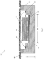
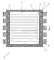
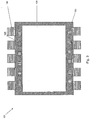
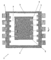
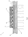
- Baugruppe (101) zur Aufnahme mindestens eines IC-Chips (103), wobei die Baugruppe Folgendes umfasst:mehrere gestapelte Schichten (113, 121), die jeweils ein keramisches Material umfassen, wobei die mehreren Schichten zur Bildung elektrischer Verbindungen (123) in der Baugruppe gestapelt sind;einen IC-Chip (103), der auf den mehreren gestapelten Schichten montiert ist;wobei mindestens eine der mehreren gestapelten Schichten eine Heizschicht (107) umfasst, wobei die Heizschicht ein keramisches Material (117) und mindestens einen Widerstandsheizfaden (115) umfasst, der auf das keramische Material der Heizschicht aufgedruckt ist;wobei der Widerstandsheizfaden zwei Enden (127) zum Empfang einer Spannung aufweist und wobei die beiden Enden mit Leitungen (109) der Baugruppe elektrisch verbunden sind; undmindestens einen Temperatursensor (115),wobei der mindestens eine Temperatursensor einen Widerstandstemperaturthermistor umfasst,wobei der mindestens eine Temperatursensor auf eine Schicht der Baugruppe aufgedruckt ist;wobei der mindestens eine Temperatursensor zwei Enden (127) zum Empfang einer Spannung aufweist, undwobei die beiden Enden mit Leitungen der Baugruppe elektrisch verbunden sind.
- Baugruppe (101) nach Anspruch 1, wobei der mindestens eine Widerstandsheizfaden (115) der Heizschicht (107) ein serpentinenförmiges Muster aufweist.
- Baugruppe (101) nach Anspruch 1, wobei der mindestens eine Temperatursensor (115) ein serpentinenförmiges Muster aufweist.
- Baugruppe (101) nach Anspruch 1,
wobei der mindestens eine Temperatursensor (115) und der mindestens eine Widerstandsheizfaden (115) der gleiche Faden (115) sind, und
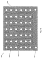
wobei ein spezifischer Widerstand des mindestens einen Heizfadens gemessen wird, um eine Temperatur der Heizschicht (107) zu messen. - Baugruppe (101) nach Anspruch 1, die weiterhin Folgendes umfasst:mehrere Chips (1103), die auf den mehreren gestapelten Schichten (113, 121) montiert sind;mehrere Widerstandsheizfäden (1409), die in der Heizschicht (1501) angeordnet sind, wobei jedes Widerstandsheizelement einen jeweiligen Chip der mehreren Chips erhitzt, wobei jeder der Widerstandsheizfäden zwei Enden (1411) zum Empfang einer Spannung aufweist und wobei die Enden mit Leitungen (109) der Baugruppe elektrisch verbunden sind.
- Baugruppe (101) nach Anspruch 5, die Folgendes umfasst:mehrere Temperatursensoren (1405), die in der Heizschicht (1501) angeordnet sind, wobei jeder der Temperatursensoren zwei Enden (1407) zum Empfang einer Spannung aufweist und wobei die mindestens zwei Enden mit Leitungen (109) der Baugruppe elektrisch verbunden sind, wobei Ausgänge jedes der mehreren Temperatursensoren verwendet werden, um eine Temperatur eines jeweiligen Chips der mehreren in der Baugruppe angeordneten Chips (103) zu schätzen.
- Baugruppe (101) nach Anspruch 1,
wobei ein Ausgang aus dem mindestens einen Temperatursensor (115) verwendet wird, um die Temperatur des Chips (103) zu schätzen, und
wobei die an den Enden (127) des mindestens einen Widerstandsheizfadens (115) angelegte Spannung als Reaktion auf die geschätzte Temperatur des Chips geändert wird. - Baugruppe (101) nach Anspruch 6,
wobei die Spannung, die an einen Widerstandsheizfaden (1409) angelegt wird, der die Umgebung mindestens eines der in der Baugruppe angeordneten mehreren Chips (1103) erhitzt, als Reaktion auf die geschätzte Temperatur mindestens eines mehrerer in der Baugruppe angeordneter Chips geändert wird. - Baugruppe (101) nach Anspruch 1, wobei der IC-Chip (103) zu oder nach dem Zeitpunkt, zu dem der mindestens eine Chip durch den mindestens einen Widerstandsheizfaden (115) erhitzt wird, geprüft wird.
- Baugruppe (101) nach Anspruch 1, die weiterhin eine Prüfkomponente umfasst, die dazu konfiguriert ist, den IC-Chip (103) zu prüfen,
wobei die Heizschicht (107) dazu konfiguriert ist, eine Spannung an die Enden (127) des mindestens einen Widerstandsheizfadens (115) anzulegen, der die Umgebung mindestens eines fehlerhaften IC-Chips auf eine Temperatur erhitzt, bei der ein Material (105), das zur Befestigung des mindestens einen fehlerhaften IC-Chips an der keramischen Schicht (113, 117) verwendet wird, geschwächt wird, wenn die Prüfkomponente bestimmt, dass die mindestens eine fehlerhafte integrierte Schaltung fehlerhaft ist, um die mindestens eine fehlerhafte integrierte Schaltung von der Baugruppe zu entfernen.
Applications Claiming Priority (1)
| Application Number | Priority Date | Filing Date | Title |
|---|---|---|---|
| US12/172,317 US7965094B2 (en) | 2008-07-14 | 2008-07-14 | Packaged die heater |
Publications (2)
| Publication Number | Publication Date |
|---|---|
| EP2146214A1 EP2146214A1 (de) | 2010-01-20 |
| EP2146214B1 true EP2146214B1 (de) | 2011-01-26 |
Family
ID=41262269
Family Applications (1)
| Application Number | Title | Priority Date | Filing Date |
|---|---|---|---|
| EP09159277A Not-in-force EP2146214B1 (de) | 2008-07-14 | 2009-05-01 | Erhitzer für kompakten Chip |
Country Status (5)
| Country | Link |
|---|---|
| US (1) | US7965094B2 (de) |
| EP (1) | EP2146214B1 (de) |
| JP (1) | JP5484783B2 (de) |
| AT (1) | ATE497173T1 (de) |
| DE (1) | DE602009000664D1 (de) |
Families Citing this family (25)
| Publication number | Priority date | Publication date | Assignee | Title |
|---|---|---|---|---|
| US9804223B2 (en) * | 2009-11-30 | 2017-10-31 | Essai, Inc. | Systems and methods for conforming test tooling to integrated circuit device with heater socket |
| US20150022226A1 (en) * | 2009-11-30 | 2015-01-22 | Essai, Inc. | Systems and methods for conforming test tooling to integrated circuit device profiles with coaxial socket |
| US8756549B2 (en) | 2011-01-05 | 2014-06-17 | International Business Machines Corporation | Integrated circuit chip incorporating embedded thermal radiators for localized, on-demand, heating and a system and method for designing such an integrated circuit chip |
| US10109606B2 (en) | 2011-10-27 | 2018-10-23 | Global Circuit Innovations, Inc. | Remapped packaged extracted die |
| US9935028B2 (en) | 2013-03-05 | 2018-04-03 | Global Circuit Innovations Incorporated | Method and apparatus for printing integrated circuit bond connections |
| US10177054B2 (en) | 2011-10-27 | 2019-01-08 | Global Circuit Innovations, Inc. | Method for remapping a packaged extracted die |
| US10147660B2 (en) | 2011-10-27 | 2018-12-04 | Global Circuits Innovations, Inc. | Remapped packaged extracted die with 3D printed bond connections |
| US9870968B2 (en) | 2011-10-27 | 2018-01-16 | Global Circuit Innovations Incorporated | Repackaged integrated circuit and assembly method |
| US10002846B2 (en) | 2011-10-27 | 2018-06-19 | Global Circuit Innovations Incorporated | Method for remapping a packaged extracted die with 3D printed bond connections |
| US9966319B1 (en) | 2011-10-27 | 2018-05-08 | Global Circuit Innovations Incorporated | Environmental hardening integrated circuit method and apparatus |
| US10128161B2 (en) | 2011-10-27 | 2018-11-13 | Global Circuit Innovations, Inc. | 3D printed hermetic package assembly and method |
| EP2823512B1 (de) | 2012-03-07 | 2016-10-05 | Crocus Technology Inc. | Magnetische logikeinheiten zur messung einer magnetischen feldrichtung |
| KR20140106997A (ko) * | 2013-02-27 | 2014-09-04 | 삼성전자주식회사 | 반도체 패키지 |
| JP5782070B2 (ja) * | 2013-07-19 | 2015-09-24 | 日本電信電話株式会社 | 電気素子のパッケージ |
| JP6280519B2 (ja) * | 2015-05-01 | 2018-02-14 | 株式会社ヒットデバイス | 電子部品の温度特性評価装置およびそれに用いられる温度制御ユニット |
| US10499461B2 (en) * | 2015-12-21 | 2019-12-03 | Intel Corporation | Thermal head with a thermal barrier for integrated circuit die processing |
| JP2018100838A (ja) * | 2016-12-19 | 2018-06-28 | ルネサスエレクトロニクス株式会社 | 半導体製造装置、半導体製造方法及び半導体装置 |
| US10782316B2 (en) * | 2017-01-09 | 2020-09-22 | Delta Design, Inc. | Socket side thermal system |
| CN107860483A (zh) * | 2017-12-26 | 2018-03-30 | 上海理好智能科技有限公司 | 一种带温度传感器的发热器及其制备方法 |
| US10115645B1 (en) | 2018-01-09 | 2018-10-30 | Global Circuit Innovations, Inc. | Repackaged reconditioned die method and assembly |
| CN108622847A (zh) * | 2018-05-03 | 2018-10-09 | 河北美泰电子科技有限公司 | Mems传感器的封装方法及封装结构 |
| US20220413015A1 (en) * | 2019-11-27 | 2022-12-29 | Kyocera Corporation | Circuit board, probe card substrate, and probe card |
| US11508680B2 (en) | 2020-11-13 | 2022-11-22 | Global Circuit Innovations Inc. | Solder ball application for singular die |
| CN113097200B (zh) * | 2021-03-09 | 2022-09-20 | 中国电子科技集团公司第二十九研究所 | 一种倒装热源芯片及其制备方法和应用方法 |
| EP4364197A1 (de) | 2021-06-30 | 2024-05-08 | Delta Design, Inc. | Temperatursteuerungssystem mit schützanordnung |
Family Cites Families (24)
| Publication number | Priority date | Publication date | Assignee | Title |
|---|---|---|---|---|
| US3914639A (en) * | 1974-04-05 | 1975-10-21 | Anthony J Barraco | Heater unit for cathode |
| JPS51144182A (en) * | 1975-06-05 | 1976-12-10 | Mitsubishi Electric Corp | Indirectly heated semiconductor unit |
| US4561006A (en) * | 1982-07-06 | 1985-12-24 | Sperry Corporation | Integrated circuit package with integral heating circuit |
| US4777434A (en) * | 1985-10-03 | 1988-10-11 | Amp Incorporated | Microelectronic burn-in system |
| US4968931A (en) * | 1989-11-03 | 1990-11-06 | Motorola, Inc. | Apparatus and method for burning in integrated circuit wafers |
| US5663654A (en) * | 1990-08-29 | 1997-09-02 | Micron Technology, Inc. | Universal wafer carrier for wafer level die burn-in |
| CA2073886A1 (en) * | 1991-07-19 | 1993-01-20 | Tatsuya Hashinaga | Burn-in apparatus and method |
| JPH0595076A (ja) * | 1991-10-01 | 1993-04-16 | Seiko Epson Corp | 半導体装置 |
| KR0140034B1 (ko) * | 1993-12-16 | 1998-07-15 | 모리시다 요이치 | 반도체 웨이퍼 수납기, 반도체 웨이퍼의 검사용 집적회로 단자와 프로브 단자와의 접속방법 및 그 장치, 반도체 집적회로의 검사방법, 프로브카드 및 그 제조방법 |
| US5451165A (en) * | 1994-07-27 | 1995-09-19 | Minnesota Mining And Manufacturing Company | Temporary package for bare die test and burn-in |
| US6041729A (en) * | 1995-10-06 | 2000-03-28 | Alan; Brad | Mooring line receptacle apparatus |
| JP2002110751A (ja) * | 2000-10-03 | 2002-04-12 | Hitachi Ltd | 半導体集積回路装置の検査装置および製造方法 |
| GB2368140A (en) | 2000-10-19 | 2002-04-24 | Bookham Technology Plc | Integrated optical device with heaters |
| JP3825277B2 (ja) * | 2001-05-25 | 2006-09-27 | 東京エレクトロン株式会社 | 加熱処理装置 |
| JP3768845B2 (ja) | 2001-07-13 | 2006-04-19 | キヤノン株式会社 | 光学素子の成形装置 |
| US6666907B1 (en) * | 2002-01-31 | 2003-12-23 | Sandia Corporation | Temperature programmable microfabricated gas chromatography column |
| JP2004206861A (ja) | 2002-12-13 | 2004-07-22 | Matsushita Electric Ind Co Ltd | 空き領域の検索方法および検索装置、記録済み領域の配置の検証方法および検証装置 |
| JP2007511052A (ja) * | 2003-11-07 | 2007-04-26 | セレリティ・インコーポレイテッド | 表面実装ヒーター |
| JP4318108B2 (ja) | 2003-12-07 | 2009-08-19 | 敬 高橋 | 散水融雪方法 |
| US20060290370A1 (en) * | 2004-02-27 | 2006-12-28 | Wells-Cti, Llc, An Oregon Limited Liability Company | Temperature control in ic sockets |
| JP4281605B2 (ja) * | 2004-04-08 | 2009-06-17 | 住友電気工業株式会社 | 半導体加熱装置 |
| US7047626B2 (en) * | 2004-07-15 | 2006-05-23 | Bulk Molding Compounds, Inc. | Encapsulated electrically resistive heater |
| US20070030019A1 (en) * | 2005-08-04 | 2007-02-08 | Micron Technology, Inc. | Power sink for IC temperature control |
| US7626144B2 (en) * | 2005-09-29 | 2009-12-01 | Mikhail Merzliakov | Method and apparatus for rapid temperature changes |
-
2008
- 2008-07-14 US US12/172,317 patent/US7965094B2/en not_active Expired - Fee Related
-
2009
- 2009-05-01 DE DE602009000664T patent/DE602009000664D1/de active Active
- 2009-05-01 AT AT09159277T patent/ATE497173T1/de not_active IP Right Cessation
- 2009-05-01 EP EP09159277A patent/EP2146214B1/de not_active Not-in-force
- 2009-05-13 JP JP2009116432A patent/JP5484783B2/ja not_active Expired - Fee Related
Also Published As
| Publication number | Publication date |
|---|---|
| DE602009000664D1 (de) | 2011-03-10 |
| JP2010021530A (ja) | 2010-01-28 |
| EP2146214A1 (de) | 2010-01-20 |
| ATE497173T1 (de) | 2011-02-15 |
| JP5484783B2 (ja) | 2014-05-07 |
| US20100007367A1 (en) | 2010-01-14 |
| US7965094B2 (en) | 2011-06-21 |
Similar Documents
| Publication | Publication Date | Title |
|---|---|---|
| EP2146214B1 (de) | Erhitzer für kompakten Chip | |
| KR102212941B1 (ko) | 적재대 및 전자 디바이스 검사 장치 | |
| US6121576A (en) | Method and process of contact to a heat softened solder ball array | |
| EP1840981B1 (de) | Thermoelektrisches Modul | |
| US6504392B2 (en) | Actively controlled heat sink for convective burn-in oven | |
| US10197623B2 (en) | Heatable interposer for temperature-controlled testing of semiconductor devices | |
| CN109983350B (zh) | 载置台和电子器件测试装置 | |
| JP5851878B2 (ja) | 半導体モジュールの製造方法 | |
| KR20080069049A (ko) | 반도체 소자의 테스트 소켓 및 이를 이용한 반도체 소자의테스트 방법 | |
| US11454601B2 (en) | Substrate evaluation chip and substrate evaluation device | |
| JP2010091443A (ja) | 温度測定用半導体装置、半導体装置の温度測定システムおよび半導体装置の温度測定方法 | |
| US11221358B2 (en) | Placement stand and electronic device inspecting apparatus | |
| Weilguni et al. | Characterization of the thermal impedance of high–power LED assembly based on innovative printed circuit board technology | |
| CN111736052B (zh) | 探针卡、具有其的晶圆检测设备及使用其的裸晶测试流程 | |
| Stoukatch et al. | Low Thermal Conductivity Adhesive as a Key Enabler for Compact, Low-Cost Packaging for Metal-Oxide Gas Sensors | |
| CN111446232A (zh) | 一种芯片封装件 | |
| WO2017088286A1 (zh) | 一种倒装芯片的倒装封装结构及倒装芯片 | |
| KR101868347B1 (ko) | 반도체 패키지의 시험 장치 | |
| CN101806815A (zh) | 用于SiC MESFET直流测试的夹具 | |
| CN216389354U (zh) | 一种测试用封装基板及测试系统 | |
| WO2001006273A9 (en) | Apparatus and method for temperature control of ic device during test | |
| CN110268273A (zh) | 插孔侧热系统 | |
| JP2004325363A (ja) | 実装済みプリント基板の検査方法およびプリント基板 | |
| Wai et al. | Development of a flexible printed multi-functional sensor platform for medical applications | |
| CN117491834A (zh) | 一种表面贴装器件Rth(j-c)测试结构及测试方法 |
Legal Events
| Date | Code | Title | Description |
|---|---|---|---|
| PUAI | Public reference made under article 153(3) epc to a published international application that has entered the european phase |
Free format text: ORIGINAL CODE: 0009012 |
|
| 17P | Request for examination filed |
Effective date: 20090501 |
|
| AK | Designated contracting states |
Kind code of ref document: A1 Designated state(s): AT BE BG CH CY CZ DE DK EE ES FI FR GB GR HR HU IE IS IT LI LT LU LV MC MK MT NL NO PL PT RO SE SI SK TR |
|
| GRAP | Despatch of communication of intention to grant a patent |
Free format text: ORIGINAL CODE: EPIDOSNIGR1 |
|
| RIC1 | Information provided on ipc code assigned before grant |
Ipc: G01R 31/28 20060101ALI20100915BHEP Ipc: G01R 31/319 20060101AFI20100915BHEP |
|
| RAP1 | Party data changed (applicant data changed or rights of an application transferred) |
Owner name: HONEYWELL INTERNATIONAL, INC. |
|
| GRAS | Grant fee paid |
Free format text: ORIGINAL CODE: EPIDOSNIGR3 |
|
| GRAA | (expected) grant |
Free format text: ORIGINAL CODE: 0009210 |
|
| AK | Designated contracting states |
Kind code of ref document: B1 Designated state(s): AT BE BG CH CY CZ DE DK EE ES FI FR GB GR HR HU IE IS IT LI LT LU LV MC MK MT NL NO PL PT RO SE SI SK TR |
|
| REG | Reference to a national code |
Ref country code: GB Ref legal event code: FG4D |
|
| REG | Reference to a national code |
Ref country code: CH Ref legal event code: EP |
|
| REG | Reference to a national code |
Ref country code: IE Ref legal event code: FG4D |
|
| REF | Corresponds to: |
Ref document number: 602009000664 Country of ref document: DE Date of ref document: 20110310 Kind code of ref document: P |
|
| REG | Reference to a national code |
Ref country code: DE Ref legal event code: R096 Ref document number: 602009000664 Country of ref document: DE Effective date: 20110310 |
|
| REG | Reference to a national code |
Ref country code: NL Ref legal event code: VDEP Effective date: 20110126 |
|
| LTIE | Lt: invalidation of european patent or patent extension |
Effective date: 20110126 |
|
| PG25 | Lapsed in a contracting state [announced via postgrant information from national office to epo] |
Ref country code: LV Free format text: LAPSE BECAUSE OF FAILURE TO SUBMIT A TRANSLATION OF THE DESCRIPTION OR TO PAY THE FEE WITHIN THE PRESCRIBED TIME-LIMIT Effective date: 20110126 Ref country code: PT Free format text: LAPSE BECAUSE OF FAILURE TO SUBMIT A TRANSLATION OF THE DESCRIPTION OR TO PAY THE FEE WITHIN THE PRESCRIBED TIME-LIMIT Effective date: 20110526 Ref country code: SE Free format text: LAPSE BECAUSE OF FAILURE TO SUBMIT A TRANSLATION OF THE DESCRIPTION OR TO PAY THE FEE WITHIN THE PRESCRIBED TIME-LIMIT Effective date: 20110126 Ref country code: HR Free format text: LAPSE BECAUSE OF FAILURE TO SUBMIT A TRANSLATION OF THE DESCRIPTION OR TO PAY THE FEE WITHIN THE PRESCRIBED TIME-LIMIT Effective date: 20110126 Ref country code: LT Free format text: LAPSE BECAUSE OF FAILURE TO SUBMIT A TRANSLATION OF THE DESCRIPTION OR TO PAY THE FEE WITHIN THE PRESCRIBED TIME-LIMIT Effective date: 20110126 Ref country code: GR Free format text: LAPSE BECAUSE OF FAILURE TO SUBMIT A TRANSLATION OF THE DESCRIPTION OR TO PAY THE FEE WITHIN THE PRESCRIBED TIME-LIMIT Effective date: 20110427 Ref country code: ES Free format text: LAPSE BECAUSE OF FAILURE TO SUBMIT A TRANSLATION OF THE DESCRIPTION OR TO PAY THE FEE WITHIN THE PRESCRIBED TIME-LIMIT Effective date: 20110507 Ref country code: NO Free format text: LAPSE BECAUSE OF FAILURE TO SUBMIT A TRANSLATION OF THE DESCRIPTION OR TO PAY THE FEE WITHIN THE PRESCRIBED TIME-LIMIT Effective date: 20110426 |
|
| PG25 | Lapsed in a contracting state [announced via postgrant information from national office to epo] |
Ref country code: FI Free format text: LAPSE BECAUSE OF FAILURE TO SUBMIT A TRANSLATION OF THE DESCRIPTION OR TO PAY THE FEE WITHIN THE PRESCRIBED TIME-LIMIT Effective date: 20110126 Ref country code: BG Free format text: LAPSE BECAUSE OF FAILURE TO SUBMIT A TRANSLATION OF THE DESCRIPTION OR TO PAY THE FEE WITHIN THE PRESCRIBED TIME-LIMIT Effective date: 20110426 Ref country code: NL Free format text: LAPSE BECAUSE OF FAILURE TO SUBMIT A TRANSLATION OF THE DESCRIPTION OR TO PAY THE FEE WITHIN THE PRESCRIBED TIME-LIMIT Effective date: 20110126 Ref country code: SI Free format text: LAPSE BECAUSE OF FAILURE TO SUBMIT A TRANSLATION OF THE DESCRIPTION OR TO PAY THE FEE WITHIN THE PRESCRIBED TIME-LIMIT Effective date: 20110126 Ref country code: PL Free format text: LAPSE BECAUSE OF FAILURE TO SUBMIT A TRANSLATION OF THE DESCRIPTION OR TO PAY THE FEE WITHIN THE PRESCRIBED TIME-LIMIT Effective date: 20110126 Ref country code: CY Free format text: LAPSE BECAUSE OF FAILURE TO SUBMIT A TRANSLATION OF THE DESCRIPTION OR TO PAY THE FEE WITHIN THE PRESCRIBED TIME-LIMIT Effective date: 20110126 Ref country code: BE Free format text: LAPSE BECAUSE OF FAILURE TO SUBMIT A TRANSLATION OF THE DESCRIPTION OR TO PAY THE FEE WITHIN THE PRESCRIBED TIME-LIMIT Effective date: 20110126 Ref country code: AT Free format text: LAPSE BECAUSE OF FAILURE TO SUBMIT A TRANSLATION OF THE DESCRIPTION OR TO PAY THE FEE WITHIN THE PRESCRIBED TIME-LIMIT Effective date: 20110126 |
|
| PG25 | Lapsed in a contracting state [announced via postgrant information from national office to epo] |
Ref country code: DK Free format text: LAPSE BECAUSE OF FAILURE TO SUBMIT A TRANSLATION OF THE DESCRIPTION OR TO PAY THE FEE WITHIN THE PRESCRIBED TIME-LIMIT Effective date: 20110126 Ref country code: EE Free format text: LAPSE BECAUSE OF FAILURE TO SUBMIT A TRANSLATION OF THE DESCRIPTION OR TO PAY THE FEE WITHIN THE PRESCRIBED TIME-LIMIT Effective date: 20110126 |
|
| PG25 | Lapsed in a contracting state [announced via postgrant information from national office to epo] |
Ref country code: CZ Free format text: LAPSE BECAUSE OF FAILURE TO SUBMIT A TRANSLATION OF THE DESCRIPTION OR TO PAY THE FEE WITHIN THE PRESCRIBED TIME-LIMIT Effective date: 20110126 Ref country code: RO Free format text: LAPSE BECAUSE OF FAILURE TO SUBMIT A TRANSLATION OF THE DESCRIPTION OR TO PAY THE FEE WITHIN THE PRESCRIBED TIME-LIMIT Effective date: 20110126 Ref country code: SK Free format text: LAPSE BECAUSE OF FAILURE TO SUBMIT A TRANSLATION OF THE DESCRIPTION OR TO PAY THE FEE WITHIN THE PRESCRIBED TIME-LIMIT Effective date: 20110126 |
|
| PLBE | No opposition filed within time limit |
Free format text: ORIGINAL CODE: 0009261 |
|
| STAA | Information on the status of an ep patent application or granted ep patent |
Free format text: STATUS: NO OPPOSITION FILED WITHIN TIME LIMIT |
|
| PG25 | Lapsed in a contracting state [announced via postgrant information from national office to epo] |
Ref country code: MC Free format text: LAPSE BECAUSE OF NON-PAYMENT OF DUE FEES Effective date: 20110531 Ref country code: MT Free format text: LAPSE BECAUSE OF FAILURE TO SUBMIT A TRANSLATION OF THE DESCRIPTION OR TO PAY THE FEE WITHIN THE PRESCRIBED TIME-LIMIT Effective date: 20110126 |
|
| 26N | No opposition filed |
Effective date: 20111027 |
|
| REG | Reference to a national code |
Ref country code: DE Ref legal event code: R097 Ref document number: 602009000664 Country of ref document: DE Effective date: 20111027 |
|
| REG | Reference to a national code |
Ref country code: IE Ref legal event code: MM4A |
|
| PG25 | Lapsed in a contracting state [announced via postgrant information from national office to epo] |
Ref country code: IE Free format text: LAPSE BECAUSE OF NON-PAYMENT OF DUE FEES Effective date: 20110501 |
|
| PG25 | Lapsed in a contracting state [announced via postgrant information from national office to epo] |
Ref country code: IT Free format text: LAPSE BECAUSE OF FAILURE TO SUBMIT A TRANSLATION OF THE DESCRIPTION OR TO PAY THE FEE WITHIN THE PRESCRIBED TIME-LIMIT Effective date: 20110126 |
|
| PG25 | Lapsed in a contracting state [announced via postgrant information from national office to epo] |
Ref country code: MK Free format text: LAPSE BECAUSE OF FAILURE TO SUBMIT A TRANSLATION OF THE DESCRIPTION OR TO PAY THE FEE WITHIN THE PRESCRIBED TIME-LIMIT Effective date: 20110126 |
|
| PG25 | Lapsed in a contracting state [announced via postgrant information from national office to epo] |
Ref country code: LU Free format text: LAPSE BECAUSE OF NON-PAYMENT OF DUE FEES Effective date: 20110501 |
|
| PG25 | Lapsed in a contracting state [announced via postgrant information from national office to epo] |
Ref country code: IS Free format text: LAPSE BECAUSE OF FAILURE TO SUBMIT A TRANSLATION OF THE DESCRIPTION OR TO PAY THE FEE WITHIN THE PRESCRIBED TIME-LIMIT Effective date: 20110126 |
|
| PG25 | Lapsed in a contracting state [announced via postgrant information from national office to epo] |
Ref country code: TR Free format text: LAPSE BECAUSE OF FAILURE TO SUBMIT A TRANSLATION OF THE DESCRIPTION OR TO PAY THE FEE WITHIN THE PRESCRIBED TIME-LIMIT Effective date: 20110126 |
|
| PG25 | Lapsed in a contracting state [announced via postgrant information from national office to epo] |
Ref country code: HU Free format text: LAPSE BECAUSE OF FAILURE TO SUBMIT A TRANSLATION OF THE DESCRIPTION OR TO PAY THE FEE WITHIN THE PRESCRIBED TIME-LIMIT Effective date: 20110126 |
|
| REG | Reference to a national code |
Ref country code: CH Ref legal event code: PL |
|
| GBPC | Gb: european patent ceased through non-payment of renewal fee |
Effective date: 20130501 |
|
| PG25 | Lapsed in a contracting state [announced via postgrant information from national office to epo] |
Ref country code: CH Free format text: LAPSE BECAUSE OF NON-PAYMENT OF DUE FEES Effective date: 20130531 Ref country code: LI Free format text: LAPSE BECAUSE OF NON-PAYMENT OF DUE FEES Effective date: 20130531 |
|
| PG25 | Lapsed in a contracting state [announced via postgrant information from national office to epo] |
Ref country code: GB Free format text: LAPSE BECAUSE OF NON-PAYMENT OF DUE FEES Effective date: 20130501 |
|
| REG | Reference to a national code |
Ref country code: FR Ref legal event code: PLFP Year of fee payment: 7 |
|
| PGFP | Annual fee paid to national office [announced via postgrant information from national office to epo] |
Ref country code: DE Payment date: 20150601 Year of fee payment: 7 |
|
| PGFP | Annual fee paid to national office [announced via postgrant information from national office to epo] |
Ref country code: FR Payment date: 20150424 Year of fee payment: 7 |
|
| REG | Reference to a national code |
Ref country code: DE Ref legal event code: R119 Ref document number: 602009000664 Country of ref document: DE |
|
| REG | Reference to a national code |
Ref country code: FR Ref legal event code: ST Effective date: 20170131 |
|
| PG25 | Lapsed in a contracting state [announced via postgrant information from national office to epo] |
Ref country code: DE Free format text: LAPSE BECAUSE OF NON-PAYMENT OF DUE FEES Effective date: 20161201 Ref country code: FR Free format text: LAPSE BECAUSE OF NON-PAYMENT OF DUE FEES Effective date: 20160531 |
|
| P01 | Opt-out of the competence of the unified patent court (upc) registered |
Effective date: 20230525 |