EP2146214B1 - Packaged die heater - Google Patents
Packaged die heater Download PDFInfo
- Publication number
- EP2146214B1 EP2146214B1 EP09159277A EP09159277A EP2146214B1 EP 2146214 B1 EP2146214 B1 EP 2146214B1 EP 09159277 A EP09159277 A EP 09159277A EP 09159277 A EP09159277 A EP 09159277A EP 2146214 B1 EP2146214 B1 EP 2146214B1
- Authority
- EP
- European Patent Office
- Prior art keywords
- package
- die
- heater
- temperature
- integrated circuit
- Prior art date
- Legal status (The legal status is an assumption and is not a legal conclusion. Google has not performed a legal analysis and makes no representation as to the accuracy of the status listed.)
- Not-in-force
Links
- 238000012360 testing method Methods 0.000 claims abstract description 48
- 239000000919 ceramic Substances 0.000 claims abstract description 42
- 238000010438 heat treatment Methods 0.000 claims abstract description 40
- 239000000463 material Substances 0.000 claims abstract description 9
- 229910010293 ceramic material Inorganic materials 0.000 claims description 5
- 238000000034 method Methods 0.000 abstract description 20
- 229910052751 metal Inorganic materials 0.000 abstract description 7
- 239000002184 metal Substances 0.000 abstract description 7
- 230000035882 stress Effects 0.000 description 10
- 238000012546 transfer Methods 0.000 description 5
- BASFCYQUMIYNBI-UHFFFAOYSA-N platinum Chemical compound [Pt] BASFCYQUMIYNBI-UHFFFAOYSA-N 0.000 description 4
- 230000032683 aging Effects 0.000 description 3
- 230000006870 function Effects 0.000 description 3
- 239000004065 semiconductor Substances 0.000 description 3
- 239000004593 Epoxy Substances 0.000 description 2
- ZOKXTWBITQBERF-UHFFFAOYSA-N Molybdenum Chemical compound [Mo] ZOKXTWBITQBERF-UHFFFAOYSA-N 0.000 description 2
- 238000004891 communication Methods 0.000 description 2
- PMHQVHHXPFUNSP-UHFFFAOYSA-M copper(1+);methylsulfanylmethane;bromide Chemical compound Br[Cu].CSC PMHQVHHXPFUNSP-UHFFFAOYSA-M 0.000 description 2
- 229910052750 molybdenum Inorganic materials 0.000 description 2
- 239000011733 molybdenum Substances 0.000 description 2
- 238000012544 monitoring process Methods 0.000 description 2
- 230000003287 optical effect Effects 0.000 description 2
- 239000004033 plastic Substances 0.000 description 2
- 229910052697 platinum Inorganic materials 0.000 description 2
- 231100000812 repeated exposure Toxicity 0.000 description 2
- 229910000679 solder Inorganic materials 0.000 description 2
- 239000007787 solid Substances 0.000 description 2
- WFKWXMTUELFFGS-UHFFFAOYSA-N tungsten Chemical compound [W] WFKWXMTUELFFGS-UHFFFAOYSA-N 0.000 description 2
- 229910052721 tungsten Inorganic materials 0.000 description 2
- 239000010937 tungsten Substances 0.000 description 2
- 229910001316 Ag alloy Inorganic materials 0.000 description 1
- 229910000978 Pb alloy Inorganic materials 0.000 description 1
- 229910001128 Sn alloy Inorganic materials 0.000 description 1
- OFLYIWITHZJFLS-UHFFFAOYSA-N [Si].[Au] Chemical compound [Si].[Au] OFLYIWITHZJFLS-UHFFFAOYSA-N 0.000 description 1
- 239000000853 adhesive Substances 0.000 description 1
- 230000001070 adhesive effect Effects 0.000 description 1
- 229910052782 aluminium Inorganic materials 0.000 description 1
- XAGFODPZIPBFFR-UHFFFAOYSA-N aluminium Chemical compound [Al] XAGFODPZIPBFFR-UHFFFAOYSA-N 0.000 description 1
- PNEYBMLMFCGWSK-UHFFFAOYSA-N aluminium oxide Inorganic materials [O-2].[O-2].[O-2].[Al+3].[Al+3] PNEYBMLMFCGWSK-UHFFFAOYSA-N 0.000 description 1
- 230000009286 beneficial effect Effects 0.000 description 1
- 239000011230 binding agent Substances 0.000 description 1
- 239000003990 capacitor Substances 0.000 description 1
- 239000004020 conductor Substances 0.000 description 1
- 239000004643 cyanate ester Substances 0.000 description 1
- 230000001419 dependent effect Effects 0.000 description 1
- 238000009713 electroplating Methods 0.000 description 1
- 230000007613 environmental effect Effects 0.000 description 1
- 230000006353 environmental stress Effects 0.000 description 1
- 239000012530 fluid Substances 0.000 description 1
- 230000008642 heat stress Effects 0.000 description 1
- 239000007788 liquid Substances 0.000 description 1
- 230000007774 longterm Effects 0.000 description 1
- 150000002736 metal compounds Chemical class 0.000 description 1
- 229910044991 metal oxide Inorganic materials 0.000 description 1
- 150000004706 metal oxides Chemical class 0.000 description 1
- 239000005300 metallic glass Substances 0.000 description 1
- 229920000620 organic polymer Polymers 0.000 description 1
- TWNQGVIAIRXVLR-UHFFFAOYSA-N oxo(oxoalumanyloxy)alumane Chemical compound O=[Al]O[Al]=O TWNQGVIAIRXVLR-UHFFFAOYSA-N 0.000 description 1
- HBEQXAKJSGXAIQ-UHFFFAOYSA-N oxopalladium Chemical compound [Pd]=O HBEQXAKJSGXAIQ-UHFFFAOYSA-N 0.000 description 1
- 238000004806 packaging method and process Methods 0.000 description 1
- 229910003445 palladium oxide Inorganic materials 0.000 description 1
- 239000000843 powder Substances 0.000 description 1
- 230000002035 prolonged effect Effects 0.000 description 1
- 239000000523 sample Substances 0.000 description 1
- 238000010008 shearing Methods 0.000 description 1
- 239000004332 silver Substances 0.000 description 1
- 238000005476 soldering Methods 0.000 description 1
- 230000000153 supplemental effect Effects 0.000 description 1
Images


Classifications
-
- G—PHYSICS
- G01—MEASURING; TESTING
- G01R—MEASURING ELECTRIC VARIABLES; MEASURING MAGNETIC VARIABLES
- G01R31/00—Arrangements for testing electric properties; Arrangements for locating electric faults; Arrangements for electrical testing characterised by what is being tested not provided for elsewhere
- G01R31/28—Testing of electronic circuits, e.g. by signal tracer
- G01R31/2851—Testing of integrated circuits [IC]
- G01R31/2855—Environmental, reliability or burn-in testing
- G01R31/2872—Environmental, reliability or burn-in testing related to electrical or environmental aspects, e.g. temperature, humidity, vibration, nuclear radiation
- G01R31/2874—Environmental, reliability or burn-in testing related to electrical or environmental aspects, e.g. temperature, humidity, vibration, nuclear radiation related to temperature
- G01R31/2875—Environmental, reliability or burn-in testing related to electrical or environmental aspects, e.g. temperature, humidity, vibration, nuclear radiation related to temperature related to heating
-
- H—ELECTRICITY
- H01—ELECTRIC ELEMENTS
- H01L—SEMICONDUCTOR DEVICES NOT COVERED BY CLASS H10
- H01L2224/00—Indexing scheme for arrangements for connecting or disconnecting semiconductor or solid-state bodies and methods related thereto as covered by H01L24/00
- H01L2224/01—Means for bonding being attached to, or being formed on, the surface to be connected, e.g. chip-to-package, die-attach, "first-level" interconnects; Manufacturing methods related thereto
- H01L2224/42—Wire connectors; Manufacturing methods related thereto
- H01L2224/44—Structure, shape, material or disposition of the wire connectors prior to the connecting process
- H01L2224/45—Structure, shape, material or disposition of the wire connectors prior to the connecting process of an individual wire connector
- H01L2224/45001—Core members of the connector
- H01L2224/45099—Material
- H01L2224/451—Material with a principal constituent of the material being a metal or a metalloid, e.g. boron (B), silicon (Si), germanium (Ge), arsenic (As), antimony (Sb), tellurium (Te) and polonium (Po), and alloys thereof
- H01L2224/45117—Material with a principal constituent of the material being a metal or a metalloid, e.g. boron (B), silicon (Si), germanium (Ge), arsenic (As), antimony (Sb), tellurium (Te) and polonium (Po), and alloys thereof the principal constituent melting at a temperature of greater than or equal to 400°C and less than 950°C
- H01L2224/45124—Aluminium (Al) as principal constituent
-
- H—ELECTRICITY
- H01—ELECTRIC ELEMENTS
- H01L—SEMICONDUCTOR DEVICES NOT COVERED BY CLASS H10
- H01L2224/00—Indexing scheme for arrangements for connecting or disconnecting semiconductor or solid-state bodies and methods related thereto as covered by H01L24/00
- H01L2224/01—Means for bonding being attached to, or being formed on, the surface to be connected, e.g. chip-to-package, die-attach, "first-level" interconnects; Manufacturing methods related thereto
- H01L2224/42—Wire connectors; Manufacturing methods related thereto
- H01L2224/44—Structure, shape, material or disposition of the wire connectors prior to the connecting process
- H01L2224/45—Structure, shape, material or disposition of the wire connectors prior to the connecting process of an individual wire connector
- H01L2224/45001—Core members of the connector
- H01L2224/45099—Material
- H01L2224/451—Material with a principal constituent of the material being a metal or a metalloid, e.g. boron (B), silicon (Si), germanium (Ge), arsenic (As), antimony (Sb), tellurium (Te) and polonium (Po), and alloys thereof
- H01L2224/45138—Material with a principal constituent of the material being a metal or a metalloid, e.g. boron (B), silicon (Si), germanium (Ge), arsenic (As), antimony (Sb), tellurium (Te) and polonium (Po), and alloys thereof the principal constituent melting at a temperature of greater than or equal to 950°C and less than 1550°C
- H01L2224/45144—Gold (Au) as principal constituent
-
- H—ELECTRICITY
- H01—ELECTRIC ELEMENTS
- H01L—SEMICONDUCTOR DEVICES NOT COVERED BY CLASS H10
- H01L2224/00—Indexing scheme for arrangements for connecting or disconnecting semiconductor or solid-state bodies and methods related thereto as covered by H01L24/00
- H01L2224/01—Means for bonding being attached to, or being formed on, the surface to be connected, e.g. chip-to-package, die-attach, "first-level" interconnects; Manufacturing methods related thereto
- H01L2224/42—Wire connectors; Manufacturing methods related thereto
- H01L2224/47—Structure, shape, material or disposition of the wire connectors after the connecting process
- H01L2224/48—Structure, shape, material or disposition of the wire connectors after the connecting process of an individual wire connector
- H01L2224/4805—Shape
- H01L2224/4809—Loop shape
- H01L2224/48091—Arched
-
- H—ELECTRICITY
- H01—ELECTRIC ELEMENTS
- H01L—SEMICONDUCTOR DEVICES NOT COVERED BY CLASS H10
- H01L2224/00—Indexing scheme for arrangements for connecting or disconnecting semiconductor or solid-state bodies and methods related thereto as covered by H01L24/00
- H01L2224/73—Means for bonding being of different types provided for in two or more of groups H01L2224/10, H01L2224/18, H01L2224/26, H01L2224/34, H01L2224/42, H01L2224/50, H01L2224/63, H01L2224/71
- H01L2224/732—Location after the connecting process
- H01L2224/73251—Location after the connecting process on different surfaces
- H01L2224/73265—Layer and wire connectors
Definitions
- the present invention relates generally to heating integrated circuits for the purposes of testing and accelerated aging, and monitoring the temperature of integrated circuits during testing and accelerated aging. More particularly, the invention relates to heating integrated circuits in a package to a predetermined temperature.
- Integrated circuit die may need to be heated for multiple purposes.
- the die may be heated in order to determine performance at the operating temperature range specified for that die, to perform accelerated life testing by heating the die beyond the specified temperature range to induce accelerated aging, or to heat the die to a preset temperature in order to eliminate those die that may experience early failure.
- Integrated circuits may need to be designed to function at different operating temperature ranges based on their intended use. These circuits may be tested at the maximum temperature of the operating temperature range in order to ensure that each individual die can perform at that temperature. Typically, industrial electronics may require that the integrated circuits operate at 85° C, and other high-temperature applications, such as some military electronics, may require the integrated circuits to operate at a temperature of 125° C or higher.
- the die of integrated circuits may fail over time due to stresses from temperature variations.
- the die may be heated to a temperature beyond the specified operating range in order to perform accelerated life testing, i.e ., to heat the die to various temperatures in order to approximate the die's ability to withstand environmental stresses.
- the integrated circuits may also be tested to verify the connections between the die contacts and the package contacts. During the life cycle of the die, the connections between the die and the package may fail. Thus, by performing accelerated life testing on a packaged die, failures in the connections between the die and the package may be detected.
- die are heated in an oven to bring the die to the desired heat testing temperature.
- the die may be batch-heated in a package, and may all be heated to the same temperature in the oven.
- the die may be tested to determine performance at elevated temperatures. Heating the die in an oven may require that testing components such as connectors, printed wiring boards, sockets, resistors, capacitors, and driver chips be located inside the oven enclosure, and thus the testing components may undergo significant stress due to prolonged exposure to elevated temperatures.
- a multi-chip module may comprise several die in a single package.
- the MCM may fail if a single die fails. Thus, it may be undesirable to heat-test the die after incorporating multiple die into a single package, as all the die in the MCM may be discarded if a single die fails.
- WO02/056073 discloses an integrated optical package comprising an integrated optical device, a pair of planar heaters disposed on either side of the device, the heater is being separated from the device by a fluid gap.
- US 2007/0030019 discloses the use of a power sink function in integrated circuit testing using a method for testing integrated circuits and assembled modules at elevated temperature without the use of environmental ovens.
- US 5, 945, 834 discloses a retainer board, holding a semiconductor wafer having a plurality of integrated circuit terminals for testing a semiconductor chip.
- JP 2003 026432 discloses a semiconductor assembly comprising heating elements.
- US 2006/0290370 discloses a system and method for temperature control of integrated circuits and a system for testing integrated circuit packages comprising socket bases on a testing board for receiving a plurality of integrated circuit packages.
- the present invention relates to a heater for an integrated circuit die and a temperature sensor for sensing the temperature of an integrated circuit die.
- the heater may be contained inside the die package, or, alternatively, it may be external to the package.
- the heater incorporated into the integrated circuit package may be a layer of ceramic material having a heating filament screen-printed thereon and incorporated into the body of the integrated circuit package.
- the heater layer may preferably be located near the die attach area of the package. This may create a more efficient heat path from the heater to the die than that accomplished by using an oven or an external heater.
- temperature stresses on the testing components may be reduced, as the testing components may be in a lower temperature environment than when the die are heated by using an oven alone or an external heater.
- the heater has at least two leads, and when a voltage is applied across the heating filament the ceramic layer is heated and transmits heat to the die.
- the leads for the heater may be connected with the leads of the integrated circuit package.
- a package having multiple die there may be multiple heaters that may be individually controlled.
- die in the packages may be individually heated to obtain a desired temperature. This is advantageous, as individual die produce different amounts of heat during testing, which may affect the temperature of the die itself.
- the die may be removed from the package by heating the die area to weaken the die attach material without damaging the surrounding die. After the die attach is heated, the die may be more easily removed from the package than in known methods of removing faulty die such as applying hot air to heat the die attach material and shearing the die from the die attach site or by grinding the die out of the package.
- the heating element may be located inside the die package, there are not restrictions on the number of die that may be heated at a single time.
- the volume of the oven restricts the number of die that may be heated at one time.
- the number of packages that may be burned-in at one time is dependent on the number of contacts available to provide a voltage to the heating element to heat the die.
- a further advantage of the invention is that the heating filament, or, alternatively, a separate temperature thermistor, located in the heater ceramic layer may be used as a temperature sensor to measure the temperature of the die.
- the temperature sensor may have leads in electrical communication with the leads of the package. This temperature sensor may provide a more accurate die temperature reading than that which may be obtained by placing a temperature sensor on the package lid or elsewhere on a surface of the package because of its location close to the die.
- the die generates heat during operation; thus, during testing, the die gives off heat that may raise the temperature of the die and its surroundings.
- a temperature sensor located close to the die may provide accurate temperature readings for the die including the temperature changes caused by heat given off by the die while being tested. Placing a plurality of temperature sensors close to a plurality of die may provide improved temperature feedback by measuring the temperature of each die or of a plurality of dies. Thus, the temperature changes caused by heat given off by the each die during testing may be better approximated, and the testing and burn-in temperature of individual die and packages may be better controlled.
- a reusable external heater may be more economical than a heater layer located in a package, or it may be difficult to add a heater layer into certain integrated circuit packages. For instance, it may be difficult to add a ceramic heater layer into a plastic package.
- An external heater may be a simple ceramic solid plate, or it may be a ceramic heater having clearance holes for package pins to pass through.
- a solid ceramic plate heater may be used with peripheral-leaded packages such as flatpacks or quad flatpacks.
- a heater having clearance holes for package pins to pass through may be used with a pin grid array package or other type of package having contacts on its bottom surface.
- the heater may be used alone to heat the die, or it may be used in combination with an oven to attain the desired temperature. In this way, the die may be heated to a temperature above that which the heater or the oven may attain by itself.
- This method and apparatus include providing a local heater to heat packaged die to an elevated temperature.
- the heater may be incorporated into the package, or may be external to the package.
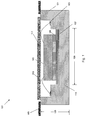
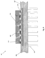
- Fig. 1 is a cutaway view of an integrated circuit package ("IC package") 101.
- the integrated circuit package may be a flatpack or a quad flatpack package.
- the IC package may comprise a plurality of layers. Each layer may be formed from a ceramic, such as alumina, aluminum nitride, or another ceramic known in the art.
- a ceramic layer may be formed by adding a binder to a ceramic powder to form a flexible tape. The tape may be cut to have the desired geometry for the package to be produced. Holes may be punched into the tape, and the holes may be filled with a conductive metal to form vias.
- Connecting lines which may be formed from a conductive metal, may be screen-printed onto the tape in order to produce the desired connections within the package when the layers are stacked.
- the layers may then be stacked, laminated, and fired at a high temperature.
- the package may then be finished by electroplating the package.
- the package may receive an integrated circuit ("die").
- the bonding pads on the die may be placed in electrical communication with bonding pads on the package by wire bonding or flip-chip bonding the bonding pads of the die to the bonding pads of the package.
- a lid may be placed over the package to form a hermetic seal.
- the layers of the IC package may form the IC package base 113. Some additional layers may have an open area in their center and may be stacked onto the IC package base 113 to form package sides 121.
- the package base 113 and package sides 121 may be comprised of a plurality of layers having electrical connections therein.
- Package bonding pads 123 may be located on the package base 113 or the package sides 121. The package bonding pads are shown in Fig. 1 having package bonding pads 123 on the package sides 121, but the package bonding pads 123 may be located in any location on the IC package 101 that may form an electrical connection to the package leads 109.
- the package base 113 and package side walls form the package body 125.
- One of the layers of the IC package 101 may be a heater layer 107, discussed further with respect to Fig. 2 .
- the heater layer 107 may have a heater filament, discussed further with respect to Fig. 2 , screen-printed thereon.
- the heater layer 107 is shown extending between two package sides 121; however, the heater layer 107 may be any size.
- the heater layer 107 is shown in Fig. 1 as the top layer of the package base 113; however, the heater layer 107 may be located anywhere in the package base 113. However, locating the heater layer 107 as close as possible to the die 103 may provide advantageous heat transfer to the die 103.
- die attach 105 may be any type of die attach material known in the art, for example, alloys of tin, lead, or silver, gold-silicon, metallic glasses, or an organic adhesive such as an epoxy.
- the die 103 is placed on top of the die attach 105.
- the die attach secures the die 103 to the heater layer 107.
- Die attach 105 is shown as covering less than the entire surface of the die cavity 108. However, die attach 105 may be any shape and size suitable to attach the die 103 to the die cavity 108.
- connections 119 are formed between the die bonding pads, not shown in Fig. 1 , and the package bonding pads 123.
- the package leads 109 are composed of a conductive material.
- the package bonding pads 123 are electrically connected to the package leads 109 through metal layers in the IC package 101.
- the IC package 101 has multiple bonding pads 123, and the die has multiple die bonding pads. The process of bonding the die bonding pads to the package bonding pads 123 is well known in the art and may be accomplished, for example, by aluminum wire bonding, gold wire bonding, or tape automated bonding.
- the die 103 may be flip-chip bonded to package bonding pads 123 located on the package base 113, as discussed with respect to Figs. 6 , 8-9 .
- Methods of bonding die 103 to packages are well-known in the art and not discussed here.
- the package lid 111 seals the IC package 101.
- the seal may be a hermetic seal.
- the package lid 111 may be metal or ceramic.
- the package lid 111 may be welded, soldered, or glass-sealed to IC package 101, or may be attached according to any other method known in the art.
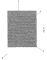
- Fig. 2 shows the heater layer 107 of IC package 101.
- the heater layer 107 may be composed of heater ceramic 117 and heater filament 115.
- Heater ceramic 117 may be any type of ceramic material, and may be the same material as the package body 125, such as, for example, aluminum oxide.
- a known ceramic having a high thermal conductivity is aluminum nitride.
- the heater filament 115 may be any type of resistive metal heating element. Tungsten, platinum, and molybdenum are known types of resistive heating elements with beneficial properties.
- the heater filament 115 may be screen-printed in a serpentine pattern. The width, depth, and length of the heater filament 115 may be varied, as well as the distance between the strands, depending on the heat output requirements of the heater layer 107.
- the heater filament 115 has two heater filament ends 127 that may connect to package leads 109 through vias located in the layers of the IC package 101. A voltage may be applied across the heater filament 115 through the package leads 109 connected to the heater filament ends 127 to produce heat to heat the die 103.
- the heater filament 115 may be any size and shape and may be connected to any of the package leads 109.
- Additional package leads 109 may be connected to each end of the heater filament 115, and may be used to estimate the temperature of the heater ceramic 117.
- the temperature of the heater ceramic 117 may be estimated by measuring the resistance of the heater filament 115 when a voltage is not being applied across the heater filament 115 to heat the heater ceramic 117.
- This configuration is known in the art as a Kelvin probe.
- a temperature sensor comprising a resistive temperature limits and a resistive eating filament are the same filament 115, as shown in figure 2 . Methods of estimating temperature by measuring the resistance of a filament are well known in the art, and are not shown in Fig. 2 .
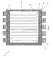
- Fig. 3 is a top view of the layer of the IC package comprising the die cavity 108, including the package body 125, package bonding pads 123, and package leads 109 of IC package 101.
- the die cavity 108 comprises a ceramic layer located over the heater ceramic 117 to electrically isolate the heater filament 115 from areas of the die 103 located on the die cavity 108.
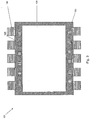
- Fig. 4 shows the die 103 having connections 119 between the die bonding pads 129 and the package bonding pads 123.
- the die 103 is shown on top of the heater layer 107, secured by die attach 105, not shown in Fig. 4 , but discussed with respect to Fig. 1 .
- Package bonding pads 123 may connected to the package leads 109 with in the layers of the IC package 101.
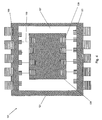
- Fig. 5 shows the IC package 101 with the package lid 111 attached.
- the package lid 111 is sealed onto the IC package as described with respect to Fig 1 .
- the package leads 109 are connected to testing components through printed wiring boards. Voltage is applied across the package leads 109 connected to the heater filament 115 in order to heat the package, and thereby heat the die 103.
- the die 103 may be tested to determine its performance at various temperatures.
- the packaged die may also be heated to test the packaged die's long-term performance under heat stresses.
- Providing a heater layer 107 inside the IC package 101 to heat the die 103 may provide advantages over the use of an oven alone to heat the die 103.
- the heater layer 107 locally heats the die 103, it may use less energy than using an oven alone.
- Heating die in an oven uses convective heat on the lid of the package to heat the die in that package. The oven must first heat the space around the package, the package lid, the space around the die, and finally the die itself.
- Providing a heater layer 107 below the die attach 105 on the IC package 101 provides a more direct heat path. Additionally, this configuration utilizes conductive heat transfer, which may be more efficient than convective heat transfer. Therefore, providing a heater layer 107 inside the IC package 101 may provide a more efficient way of heating the die 103.
- Using the heater layer 107 inside the IC package 101 to heat the die 103 may also reduce the temperature stress on the components surrounding the die 103.
- the die 103 may be heated to a preset temperature by the heater layer 107, while surrounding components may be at a lower temperature.
- Components such as the circuit boards and some parts of the packaging may have lower operating temperature requirements than those for the die 103. In this way, unnecessary stresses on surrounding components caused by high temperature exposure may be reduced.
- a package having integrated heat-testing capability may be used to heat the die alone, or in conjunction with heat applied in an oven. Temperatures inside the oven during heating may be very high, sometimes even higher than the burn-in temperature of the die 103. When die are burned in using the package having integrated heat-testing capability in conjunction with an oven, the oven temperature may be lower than when an oven alone is used to heat the die.
- testing components typically must operate inside the oven to be able to make contact with the package leads 109.
- Testing components used inside an oven may undergo repeated exposures to high temperature and may experience stress and fatigue due to these repeated exposures.
- the testing components may operate in a much lower-temperature environment by contacting the package leads 109 of a locally-heated die 103.
- fatigue and stresses on the testing components due to exposure to high temperatures is greatly reduced.
- Testing components may be very expensive or difficult to replace, and may be used repeatedly for die testing. Therefore, reducing temperature stresses on the testing components provides a significant advantage.
- the heater filament 115 may be used to sense the temperature of the heater ceramic 117 by monitoring the changes in the resistivity of the heating element.
- a separate resistive temperature sensor or sensors may be screen-printed on the heater layer 107 to act as a temperature sensor, as described with respect to Figs. 14 and 15 .
- the temperature of the heater ceramic 117 may be very close to that of the die 103.
- the temperature of the die 103 may be approximated by sensing the temperature of the package lid 111, or at another location on the IC package 119.
- the heater filament 115 or a separate temperature sensor may provide more accurate temperature data. This is useful both in controlling the temperature to which the die 103 is heated during testing, and for obtaining more accurate data on die performance at various temperatures.
- Fig. 6 shows another example of an IC package 601.
- the IC package 601 has a package base 609 with a heater layer 607 therein.
- the contact pads 611 and leads 613 are located on the bottom surface of the package base 609.
- the leads 613 may be connected to contact pads 611 through vias located within the package bottom layer 609.
- the vias are not shown in Fig. 6 , but methods of connecting leads 613 and contact pads 61 are well known in the art.
- the connections may be inside the bottom layer 609 above, below, or through the heater layer 607.
- the area between the leads 613 forms die attach area 623.
- the heater layer 607 is shown in Fig. 6 inside the package bottom layer 609.
- the heater layer 607 may be located anywhere in the package bottom layer 609. However, locating the heater layer 607 as close as possible to the die 603 may provide advantageous heat transfer to the die 603.
- the leads 613 may be any shape, and may also be rounded contacts, known in the art as a ball grid array.
- the contacts 605 on the die 603 are soldered to the contact pads 611 using a conductive solder. Methods of soldering the die 603 to contact pads 611, such as flip-chip bonding, are well known in the art.
- the die may be wire bonded to form electrical contact between the package leads and the die bonding pads, depending on the configuration of the die 103.
- the area between contacts 605 on the die 603 and the die attach area 623 may be filled with an underfill 621.
- the underfill 621 may be an organic polymer such as epoxy or cyanate ester.
- the underfill 621 may be dispensed in liquid form and may flow by capillary action underneath the die 604 to fill the area between the bottom area of the die 603 and the die attach area 623.
- Fig. 7 shows heater layer 607, having heater filament 615 and heater ceramic 617.
- the heater filament 615 has two heater filament ends 627 which may be connected to package leads though vias in the package body. Voltage may be applied across the package leads attached to the heater filament ends 629 to heat the heater ceramic 617.
- the heater layer 607 may have vias 629 that run through the heater layer 607 to form connections between the contact pads 911 and the leads 913. As described with respect to Fig. 10 , the vias 629 may be located in the bottom layer 609 and may be located outside the heater layer 607. If all vias 629 are located outside the heater layer 607, then the heater layer 607, and heater filament 615 may be formed as described with respect to Fig. 10 .
- the heater filament contacts 627 may be connected to the package leads through connections located inside the package body.
- the heater filament 615 may be formed in the heater ceramic 617 so as not to come into unintended electrical contact with the vias 629.
- the heater filament 615 may be formed as shown in Fig. 7 .
- the heater filament may also be an alternative serpentine pattern having, for example, multiple rows of heater filament 615 between the contacts 619.
- the vias 629 may have a different pattern than shown in Fig. 7 .
- the heater filament 615 may be any pattern, size, or shape, provided that the heater filament 615 does not come into unintended electrical contact with the leads 619.
- Fig. 8 shows the IC package 601 with a package lid 619 located over the die 603.
- the package lid may be sealed over the die 603 as described with respect to Fig. 1 .
- Fig. 9 shows another example of an IC package 901.
- the IC package 901 has a package bottom layer 909 with a heater layer 907 therein.
- Contact pads 911 are located on the die attach area 923 of the bottom layer 909.
- Leads 913 are located on the top surface of bottom layer 909.
- the leads 913 are connected to contact pads 911 through vias located within the package bottom layer 909.
- the leads 913 may be any shape, and may also be rounded contacts, known in the art as a ball grid array.
- the leads 913 may be a single row, or may be a column grid array having multiple rows of leads 913.
- the heater layer 907 is shown in Fig. 1 as the top layer of the IC package 901; however, the heater layer 907 may be located anywhere in the IC package 901. However, locating the heater layer 907 as close as possible to the die 103 may provide advantageous heat transfer to the die 903.
- the connections may be inside the bottom layer 909.
- the connections may be inside the bottom layer 909 above, below, or through the heater layer 907.
- the contacts on the die 903 are soldered to the package contact pads 911 using a conductive solder, and may be connected as described with respect to Fig. 9 .
- the connections are not shown in Fig. 9 , but methods of connecting leads 913 and contact pads 911 are well known in the art.
- Fig. 10 shows heater layer 907, having heater filament 915 and heater ceramic 917.
- the heater layer 907 is located inside the bottom layer 909.
- the heater filament 915 has two heater filament ends 927 across which voltage may be applied to heat the heater ceramic 917.
- the heater filament ends 927 are electrically connected to leads 913 through vias located within the bottom layer 909. These connections are not shown in Fig. 10 ; however, methods of connecting leads to a contact within the bottom layer 909 are well known to persons of skill in the art.
- the heater ceramic 917 and heater filament 913 may be formed as described with respect to Fig. 2 .
- the heater filament 915 may be any size and shape and may be connected to any of the leads 913.
- IC package 101 The advantages described with respect to IC package 101 are also advantages of the IC packages 601 and 901. Further, a plurality of die 103, 603, 903 may be attached to the receiving surface of a package 101, 601, 901, and one or more die 103, 603, 903 may be heated by the heater layer 107, 607, 907.
- the heater layer may be incorporated into a variety of integrated circuit package types and shapes, and the scope of the claims should not be limited to the packages of Figs. 1-9 , but rather in accordance with the claim language itself. In another embodiment, multiple heaters may be located inside a single package.
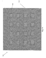
- Fig. 11 shows a die attach area 1101 of a package having a heater layer 1101 thereon.
- a plurality of die 1103 may be located on the heater layer 1105.
- the die 1103 may be attached to the heater layer 1105 according to the methods described with respect to Figs. 1-10 , or by any other method known in the art.
- the heater layer 1101 may have heater ceramic 1105 and a plurality of heater filaments thereon, located under each die 1103.
- the heater filaments may be formed as described with respect to Fig. 2 .
- Each heater filament has two leads through which a voltage may be applied to heat the die 1103.
- the heater filament leads may be connected to the package leads through connections located inside the package body, as described with respect to Fig. 10 .
- each die 1103 may be individually controlled by controlling the voltages applied to the heater filaments separately.
- changes in resistivity of the heater filament may be used to measure the temperature of the heater layer close to a single die 1103, as described with respect to Fig. 2 .
- the temperature of the die may be determined by a different temperature sensor or sensors located in the heater layer 1101, as described with respect to Fig. 15 .
- the die 1103 By heating the die 1103 with a heater layer 1105 having multiple heating filaments which may be individually controlled, different die may be heated to obtain a uniform temperature. By estimating the temperature of the die 1103 from the temperature from the resistance of the heater filament or from a separate temperature sensor, the temperature of each die 1103 may be monitored and the voltage applied to the heating filament associated with each die may be varied to obtain the desired temperature.
- Different die may have different specified temperature operating ranges. By heating individual die to different temperatures, die having low operating temperature ranges or low burn-in temperatures do not need to be heated to the same temperature as surrounding die having higher operating or burn-in temperatures. Thus, unnecessary stress on die having low operating temperature ranges or low burn-in temperatures is reduced, and the energy required for the heat testing is also reduced. Additionally, it may be advantageous to simultaneously test individual components at different temperatures. This method may provide improved data for die performance as a function of temperature.
- faulty die may be easily removed from packages. If a die is determined to be faulty after heat-testing or burn-in, the die may be removed by using the heater to locally heat the faulty die in order to weaken the die attach material, allowing the die to be more easily removed than by scribing and sawing methods. The faulty die may then be replaced.
- the heater may be external to the package.
- the external heater may be preferred for plastic packages in which it may not be possible to deposit a ceramic layer having a heating filament.
- Fig. 12 shows an external heater 1201, heater ceramic 1203, heater filament 1205, heater filament ends 1207, and heater filament leads 1209.
- the external heater 1201, heater ceramic 1203, and heater filament 1205 may be formed as described with respect to Fig. 3 .
- the heater filament leads 1209 may be located on any surface of the external heater 1201, and may be electrically connected to heater filament ends 1207 through vias located in the heater ceramic 1203. A voltage may be applied across the heater filament leads 1209 to heat IC packages located on the external heater 1201.
- the heater filament 1205 may be used to measure the temperature of the external heater to approximate the temperature of the die close to the heater filament 1205, as described with respect to Fig. 2 .
- a separate temperature sensor or sensors may be placed on the heater ceramic 1203 to estimate the temperature of the heater ceramic 1203 as described with respect to Figs. 14 and 15 .
- the external heater 1201 may have multiple heater filaments 1205, each having two heater filament leads 1207.
- the heater filaments 1205 may be individually controlled to heat the packages located on the external heater to different temperatures, as described with respect to Fig. 11 .
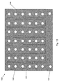
- Fig. 13 shows an external heater 1301, heater ceramic 1303, heater filament 1305, clearance holes 1309, and heater filament contacts 1307.
- the external heater 1301, heater ceramic 1303, and heater filament 1305 may be formed as described with respect to Fig. 3 .
- the clearance holes 1309 are positioned on the external heater 1301 so that package contacts may be contacted through the external heater 1301.
- the clearance holes 1309 may allow package leads to pass through the clearance holes 1309, and the clearance holes 1309 may be positioned based on the package lead locations of standard package types.
- the external heater 1301 may be positioned between the testing components and the package, so that the testing components may make electrical connection with the package contacts of the package being heated through the clearance holes 1309 of the external heater 1301.
- the heater filaments 1305 may be used to measure the temperature of the external heater to approximate the temperature of the die, as described with respect to Fig. 12 .
- the heater filaments 1305 may be individually controlled to heat the packages located on the external heater to different temperatures. Additionally, separate temperature sensors may be located near each heater filament 1305, so that the temperature of each heater filament 1305 may be accurately controlled, as described with respect to Fig. 15 .
- the heaters herein described with respect to Fig. 1-13 may be used alone or in combination with an oven to heat the packages.
- the oven could provide supplemental heat to raise the temperature of the die. Therefore, the heater may have a maximum heating capacity of less than the desired heat-testing temperature.
- the oven may be used in conjunction with the heater to raise the temperature of the die to a higher temperature than the oven alone could attain.
- a standard oven or a standard heater filament may be used for devices that required different amounts of heat to reach the desired temperatures. This provides advantages similar to those obtained using only a local heater, such as reduced energy requirements, reduced temperature stress on equipment, the ability to vary the heat testing temperature for individual die, and the ability to remove individual die from a package by heating the die attach material.
- a heater layer 1401 having a temperature sensor 1405 and a heater filament 1409 may be located within the package base.
- the temperature sensor 1405 may be a resistive temperature sensor that is screen-printed on one of the layers.
- the temperature sensor 1405 is shown in Fig. 14 having a serpentine shape; however, the temperature sensor 1405 may be any shape.
- the temperature sensor 1405 may be composed of any metal or metal compound known in the art for resistive temperature thermistors, for example, platinum, molybdenum, tungsten, palladium oxide, or other metal oxide.
- the ends 1407 of the temperature sensor 1405 and the ends 1411 of the heater filament 1409 may be electrically connected to the leads of the heater layer 1401 by forming electrical connections in the heater layer 1401.
- the temperature sensor 1405 may be located anywhere within the package. However, locating the temperature sensor 1405 close to the top of the package base, as close as possible to the die, may allow the temperature of the die to be more accurately estimated.
- a heater layer 1501 may have multiple die attach sites 1503 having a temperature sensor 1405 and a heater filament 1409 located within the package base, and formed as described with respect to Fig. 14 .
- the temperature of the die may be estimated from the temperature sensor 1405 and the voltage applied to each heater filament 1409 may be varied to obtain the desired temperature for a die located near the die attach site 1503.
Abstract
Description
- The present invention relates generally to heating integrated circuits for the purposes of testing and accelerated aging, and monitoring the temperature of integrated circuits during testing and accelerated aging. More particularly, the invention relates to heating integrated circuits in a package to a predetermined temperature.
- Integrated circuit die may need to be heated for multiple purposes. The die may be heated in order to determine performance at the operating temperature range specified for that die, to perform accelerated life testing by heating the die beyond the specified temperature range to induce accelerated aging, or to heat the die to a preset temperature in order to eliminate those die that may experience early failure.
- Integrated circuits may need to be designed to function at different operating temperature ranges based on their intended use. These circuits may be tested at the maximum temperature of the operating temperature range in order to ensure that each individual die can perform at that temperature. Typically, industrial electronics may require that the integrated circuits operate at 85° C, and other high-temperature applications, such as some military electronics, may require the integrated circuits to operate at a temperature of 125° C or higher.
- The die of integrated circuits may fail over time due to stresses from temperature variations. The die may be heated to a temperature beyond the specified operating range in order to perform accelerated life testing, i.e., to heat the die to various temperatures in order to approximate the die's ability to withstand environmental stresses.
- The integrated circuits may also be tested to verify the connections between the die contacts and the package contacts. During the life cycle of the die, the connections between the die and the package may fail. Thus, by performing accelerated life testing on a packaged die, failures in the connections between the die and the package may be detected.
- Typically, die are heated in an oven to bring the die to the desired heat testing temperature. The die may be batch-heated in a package, and may all be heated to the same temperature in the oven. The die may be tested to determine performance at elevated temperatures. Heating the die in an oven may require that testing components such as connectors, printed wiring boards, sockets, resistors, capacitors, and driver chips be located inside the oven enclosure, and thus the testing components may undergo significant stress due to prolonged exposure to elevated temperatures.
- A multi-chip module ("MCM) may comprise several die in a single package. The MCM may fail if a single die fails. Thus, it may be undesirable to heat-test the die after incorporating multiple die into a single package, as all the die in the MCM may be discarded if a single die fails.
-
WO02/056073 -
US 2007/0030019 discloses the use of a power sink function in integrated circuit testing using a method for testing integrated circuits and assembled modules at elevated temperature without the use of environmental ovens. -
US 5, 945, 834 discloses a retainer board, holding a semiconductor wafer having a plurality of integrated circuit terminals for testing a semiconductor chip. -
JP 2003 026432 -
US 2006/0290370 discloses a system and method for temperature control of integrated circuits and a system for testing integrated circuit packages comprising socket bases on a testing board for receiving a plurality of integrated circuit packages. - Therefore, an improved method of heat testing integrated circuit die is needed.
- The present invention in its various aspects is as set out in the appended claims.
- The present invention relates to a heater for an integrated circuit die and a temperature sensor for sensing the temperature of an integrated circuit die. The heater may be contained inside the die package, or, alternatively, it may be external to the package.
- The heater incorporated into the integrated circuit package may be a layer of ceramic material having a heating filament screen-printed thereon and incorporated into the body of the integrated circuit package. The heater layer may preferably be located near the die attach area of the package. This may create a more efficient heat path from the heater to the die than that accomplished by using an oven or an external heater.
- Also, temperature stresses on the testing components may be reduced, as the testing components may be in a lower temperature environment than when the die are heated by using an oven alone or an external heater.
- The heater has at least two leads, and when a voltage is applied across the heating filament the ceramic layer is heated and transmits heat to the die. The leads for the heater may be connected with the leads of the integrated circuit package.
- In a package having multiple die, there may be multiple heaters that may be individually controlled. In this way, die in the packages may be individually heated to obtain a desired temperature. This is advantageous, as individual die produce different amounts of heat during testing, which may affect the temperature of the die itself. Also, if a die is found to be faulty during testing, the die may be removed from the package by heating the die area to weaken the die attach material without damaging the surrounding die. After the die attach is heated, the die may be more easily removed from the package than in known methods of removing faulty die such as applying hot air to heat the die attach material and shearing the die from the die attach site or by grinding the die out of the package.
- Because the heating element may be located inside the die package, there are not restrictions on the number of die that may be heated at a single time. When using ovens to heat the die, the volume of the oven restricts the number of die that may be heated at one time. For packages having a heater inside, the number of packages that may be burned-in at one time is dependent on the number of contacts available to provide a voltage to the heating element to heat the die.
- A further advantage of the invention is that the heating filament, or, alternatively, a separate temperature thermistor, located in the heater ceramic layer may be used as a temperature sensor to measure the temperature of the die. The temperature sensor may have leads in electrical communication with the leads of the package. This temperature sensor may provide a more accurate die temperature reading than that which may be obtained by placing a temperature sensor on the package lid or elsewhere on a surface of the package because of its location close to the die.
- Further, the die generates heat during operation; thus, during testing, the die gives off heat that may raise the temperature of the die and its surroundings. A temperature sensor located close to the die may provide accurate temperature readings for the die including the temperature changes caused by heat given off by the die while being tested. Placing a plurality of temperature sensors close to a plurality of die may provide improved temperature feedback by measuring the temperature of each die or of a plurality of dies. Thus, the temperature changes caused by heat given off by the each die during testing may be better approximated, and the testing and burn-in temperature of individual die and packages may be better controlled.
- In some types of integrated circuit packages, it may be advantageous to provide a heater external to the integrated circuit package. A reusable external heater may be more economical than a heater layer located in a package, or it may be difficult to add a heater layer into certain integrated circuit packages. For instance, it may be difficult to add a ceramic heater layer into a plastic package. An external heater may be a simple ceramic solid plate, or it may be a ceramic heater having clearance holes for package pins to pass through. A solid ceramic plate heater may be used with peripheral-leaded packages such as flatpacks or quad flatpacks. Alternatively, a heater having clearance holes for package pins to pass through may be used with a pin grid array package or other type of package having contacts on its bottom surface.
- The heater may be used alone to heat the die, or it may be used in combination with an oven to attain the desired temperature. In this way, the die may be heated to a temperature above that which the heater or the oven may attain by itself.
- These as well as other aspects and advantages will become apparent to those of ordinary skill in the art by reading the following detailed description, with reference where appropriate to the accompanying drawings. Further, it is understood that this summary is merely an example and is not intended to limit the scope of the invention as claimed.
- Presently preferred embodiments are described below in conjunction with the appended drawing figures, wherein like reference numerals refer to like elements in the various figures, and wherein:
-
Fig. 1 is a cutaway view of an integrated circuit in a package, according to a first embodiment. -
Fig. 2 is a top view of a heater layer of the package, according to an embodiment. -
Fig. 3 is a top view of a die cavity of the package, according to an embodiment. -
Fig. 4 is a top view of the integrated circuit in the package ofFig. 1 , according to another embodiment. -
Fig. 5 is a top view of the package ofFig. 1 , having the lid installed over the integrated circuit, according to an embodiment. -
Fig. 6 is a cutaway view of an integrated circuit in a package and an integrated circuit die, according to an embodiment. -
Fig. 7 is a top view of the heater layer of the package ofFig. 6 , according to an embodiment. -
Fig. 8 is a cutaway view of the package and an integrated circuit die ofFig. 6 , having the package lid installed over the integrated circuit die, according to an embodiment;. -
Fig. 9 is a cutaway view of a package and an integrated circuit die, according to an embodiment. -
Fig. 10 is a top view of the heater layer of the package and integrated circuit die ofFig. 9 , according to an example. -
Fig. 11 is a top view of the heater layer of a package having multiple die attached thereto, according to an example. -
Fig. 12 is a top view of an external ceramic die heater, according to an example. -
Fig. 13 is a top view of an external ceramic die heater having clearance holes therethrough, according to an example. -
Fig. 14 is a top view of a layer of an integrated circuit package having a temperature sensor and a heater filament, according to an example. -
Fig. 15 is a top view of a layer of an integrated circuit package having a plurality of temperature sensors and a plurality of heater filaments, according to an example. - An improved apparatus for heating integrated circuit die is described. This method and apparatus include providing a local heater to heat packaged die to an elevated temperature. The heater may be incorporated into the package, or may be external to the package.
- The heater may be incorporated into many types of die packages.
Fig. 1 is a cutaway view of an integrated circuit package ("IC package") 101. The integrated circuit package may be a flatpack or a quad flatpack package. The IC package may comprise a plurality of layers. Each layer may be formed from a ceramic, such as alumina, aluminum nitride, or another ceramic known in the art. A ceramic layer may be formed by adding a binder to a ceramic powder to form a flexible tape. The tape may be cut to have the desired geometry for the package to be produced. Holes may be punched into the tape, and the holes may be filled with a conductive metal to form vias. Connecting lines, which may be formed from a conductive metal, may be screen-printed onto the tape in order to produce the desired connections within the package when the layers are stacked. The layers may then be stacked, laminated, and fired at a high temperature. The package may then be finished by electroplating the package. - After the package is finished, the package may receive an integrated circuit ("die"). The bonding pads on the die may be placed in electrical communication with bonding pads on the package by wire bonding or flip-chip bonding the bonding pads of the die to the bonding pads of the package. A lid may be placed over the package to form a hermetic seal. Methods and materials used to form IC packages as described above are well known in the art and not illustrated here.
- The layers of the IC package may form the
IC package base 113. Some additional layers may have an open area in their center and may be stacked onto theIC package base 113 to form package sides 121. Thepackage base 113 andpackage sides 121 may be comprised of a plurality of layers having electrical connections therein.Package bonding pads 123 may be located on thepackage base 113 or the package sides 121. The package bonding pads are shown inFig. 1 havingpackage bonding pads 123 on the package sides 121, but thepackage bonding pads 123 may be located in any location on theIC package 101 that may form an electrical connection to the package leads 109. Thepackage base 113 and package side walls form thepackage body 125. - One of the layers of the
IC package 101 may be aheater layer 107, discussed further with respect toFig. 2 . Theheater layer 107 may have a heater filament, discussed further with respect toFig. 2 , screen-printed thereon. Theheater layer 107 is shown extending between twopackage sides 121; however, theheater layer 107 may be any size. Theheater layer 107 is shown inFig. 1 as the top layer of thepackage base 113; however, theheater layer 107 may be located anywhere in thepackage base 113. However, locating theheater layer 107 as close as possible to the die 103 may provide advantageous heat transfer to thedie 103. - The area in the
package body 125 formed by the package sides 121 and thepackage base 113 is thedie cavity 108. On the top surface of the of thedie cavity 108 is deposited die attach 105. Die attach 105 may be any type of die attach material known in the art, for example, alloys of tin, lead, or silver, gold-silicon, metallic glasses, or an organic adhesive such as an epoxy. - The
die 103 is placed on top of the die attach 105. The die attach secures the die 103 to theheater layer 107. Die attach 105 is shown as covering less than the entire surface of thedie cavity 108. However, die attach 105 may be any shape and size suitable to attach thedie 103 to thedie cavity 108. - After the
die 103 has been attached to the top of thedie cavity 108 by the die attach 105,connections 119 are formed between the die bonding pads, not shown inFig. 1 , and thepackage bonding pads 123. The package leads 109 are composed of a conductive material. Thepackage bonding pads 123 are electrically connected to the package leads 109 through metal layers in theIC package 101. TheIC package 101 hasmultiple bonding pads 123, and the die has multiple die bonding pads. The process of bonding the die bonding pads to thepackage bonding pads 123 is well known in the art and may be accomplished, for example, by aluminum wire bonding, gold wire bonding, or tape automated bonding. Alternatively, thedie 103 may be flip-chip bonded to packagebonding pads 123 located on thepackage base 113, as discussed with respect toFigs. 6 ,8-9 . Methods of bonding die 103 to packages are well-known in the art and not discussed here. - The
package lid 111 seals theIC package 101. The seal may be a hermetic seal. Thepackage lid 111 may be metal or ceramic. Thepackage lid 111 may be welded, soldered, or glass-sealed toIC package 101, or may be attached according to any other method known in the art. -
Fig. 2 shows theheater layer 107 ofIC package 101. Theheater layer 107 may be composed ofheater ceramic 117 andheater filament 115.Heater ceramic 117 may be any type of ceramic material, and may be the same material as thepackage body 125, such as, for example, aluminum oxide. A known ceramic having a high thermal conductivity is aluminum nitride. Theheater filament 115 may be any type of resistive metal heating element. Tungsten, platinum, and molybdenum are known types of resistive heating elements with beneficial properties. Theheater filament 115 may be screen-printed in a serpentine pattern. The width, depth, and length of theheater filament 115 may be varied, as well as the distance between the strands, depending on the heat output requirements of theheater layer 107. - The
heater filament 115 has two heater filament ends 127 that may connect to package leads 109 through vias located in the layers of theIC package 101. A voltage may be applied across theheater filament 115 through the package leads 109 connected to the heater filament ends 127 to produce heat to heat thedie 103. Theheater filament 115 may be any size and shape and may be connected to any of the package leads 109. - Additional package leads 109 may be connected to each end of the
heater filament 115, and may be used to estimate the temperature of theheater ceramic 117. The temperature of theheater ceramic 117 may be estimated by measuring the resistance of theheater filament 115 when a voltage is not being applied across theheater filament 115 to heat theheater ceramic 117. This configuration is known in the art as a Kelvin probe. In one example, a temperature sensor comprising a resistive temperature limits and a resistive eating filament are thesame filament 115, as shown infigure 2 . Methods of estimating temperature by measuring the resistance of a filament are well known in the art, and are not shown inFig. 2 . -
Fig. 3 is a top view of the layer of the IC package comprising thedie cavity 108, including thepackage body 125,package bonding pads 123, and package leads 109 ofIC package 101. Thedie cavity 108 comprises a ceramic layer located over theheater ceramic 117 to electrically isolate theheater filament 115 from areas of the die 103 located on thedie cavity 108. -
Fig. 4 shows thedie 103 havingconnections 119 between thedie bonding pads 129 and thepackage bonding pads 123. Thedie 103 is shown on top of theheater layer 107, secured by die attach 105, not shown inFig. 4 , but discussed with respect toFig. 1 .Package bonding pads 123 may connected to the package leads 109 with in the layers of theIC package 101. -
Fig. 5 shows theIC package 101 with thepackage lid 111 attached. Thepackage lid 111 is sealed onto the IC package as described with respect toFig 1 . When thedie 103 is tested, the package leads 109 are connected to testing components through printed wiring boards. Voltage is applied across the package leads 109 connected to theheater filament 115 in order to heat the package, and thereby heat thedie 103. - The
die 103 may be tested to determine its performance at various temperatures. The packaged die may also be heated to test the packaged die's long-term performance under heat stresses. - Providing a
heater layer 107 inside theIC package 101 to heat thedie 103 may provide advantages over the use of an oven alone to heat thedie 103. First, because theheater layer 107 locally heats thedie 103, it may use less energy than using an oven alone. Heating die in an oven uses convective heat on the lid of the package to heat the die in that package. The oven must first heat the space around the package, the package lid, the space around the die, and finally the die itself. Providing aheater layer 107 below the die attach 105 on theIC package 101 provides a more direct heat path. Additionally, this configuration utilizes conductive heat transfer, which may be more efficient than convective heat transfer. Therefore, providing aheater layer 107 inside theIC package 101 may provide a more efficient way of heating thedie 103. - Using the
heater layer 107 inside theIC package 101 to heat thedie 103 may also reduce the temperature stress on the components surrounding thedie 103. Thus, thedie 103 may be heated to a preset temperature by theheater layer 107, while surrounding components may be at a lower temperature. Components such as the circuit boards and some parts of the packaging may have lower operating temperature requirements than those for thedie 103. In this way, unnecessary stresses on surrounding components caused by high temperature exposure may be reduced. - Using the
heater layer 107 inside theIC package 101 to heat thedie 103 reduces fatigue on the testing components caused by high temperature exposure. A package having integrated heat-testing capability may be used to heat the die alone, or in conjunction with heat applied in an oven. Temperatures inside the oven during heating may be very high, sometimes even higher than the burn-in temperature of thedie 103. When die are burned in using the package having integrated heat-testing capability in conjunction with an oven, the oven temperature may be lower than when an oven alone is used to heat the die. - Typically the testing components must operate inside the oven to be able to make contact with the package leads 109. Testing components used inside an oven may undergo repeated exposures to high temperature and may experience stress and fatigue due to these repeated exposures. Using the
heater layer 107 inside theIC package 101, the testing components may operate in a much lower-temperature environment by contacting the package leads 109 of a locally-heated die 103. Thus, fatigue and stresses on the testing components due to exposure to high temperatures is greatly reduced. Testing components may be very expensive or difficult to replace, and may be used repeatedly for die testing. Therefore, reducing temperature stresses on the testing components provides a significant advantage. - A further advantage is that the
heater filament 115 may be used to sense the temperature of theheater ceramic 117 by monitoring the changes in the resistivity of the heating element. Alternatively, a separate resistive temperature sensor or sensors may be screen-printed on theheater layer 107 to act as a temperature sensor, as described with respect toFigs. 14 and15 . - Because the
heater ceramic 117 is located close to the die 103 and heats thedie 103 by conduction, the temperature of theheater ceramic 117 may be very close to that of thedie 103. In oven heat testing, the temperature of thedie 103 may be approximated by sensing the temperature of thepackage lid 111, or at another location on theIC package 119. However, because the temperature of theheater ceramic 117 is much closer to the temperature of thedie 103, theheater filament 115 or a separate temperature sensor may provide more accurate temperature data. This is useful both in controlling the temperature to which thedie 103 is heated during testing, and for obtaining more accurate data on die performance at various temperatures. -
Fig. 6 shows another example of anIC package 601. TheIC package 601 has apackage base 609 with aheater layer 607 therein. Thecontact pads 611 and leads 613 are located on the bottom surface of thepackage base 609. The leads 613 may be connected to contactpads 611 through vias located within the packagebottom layer 609. The vias are not shown inFig. 6 , but methods of connectingleads 613 and contact pads 61 are well known in the art. The connections may be inside thebottom layer 609 above, below, or through theheater layer 607. The area between theleads 613 forms die attach area 623. - The
heater layer 607 is shown inFig. 6 inside the packagebottom layer 609. Theheater layer 607 may be located anywhere in the packagebottom layer 609. However, locating theheater layer 607 as close as possible to the die 603 may provide advantageous heat transfer to thedie 603. - The leads 613 may be any shape, and may also be rounded contacts, known in the art as a ball grid array. The
contacts 605 on thedie 603 are soldered to thecontact pads 611 using a conductive solder. Methods of soldering thedie 603 to contactpads 611, such as flip-chip bonding, are well known in the art. Alternatively, the die may be wire bonded to form electrical contact between the package leads and the die bonding pads, depending on the configuration of thedie 103. The area betweencontacts 605 on thedie 603 and the die attach area 623 may be filled with anunderfill 621. Theunderfill 621 may be an organic polymer such as epoxy or cyanate ester. Theunderfill 621 may be dispensed in liquid form and may flow by capillary action underneath the die 604 to fill the area between the bottom area of thedie 603 and the die attach area 623. -
Fig. 7 showsheater layer 607, havingheater filament 615 andheater ceramic 617. Theheater filament 615 has two heater filament ends 627 which may be connected to package leads though vias in the package body. Voltage may be applied across the package leads attached to the heater filament ends 629 to heat theheater ceramic 617. - The
heater layer 607 may havevias 629 that run through theheater layer 607 to form connections between the contact pads 911 and theleads 913. As described with respect toFig. 10 , thevias 629 may be located in thebottom layer 609 and may be located outside theheater layer 607. If all vias 629 are located outside theheater layer 607, then theheater layer 607, andheater filament 615 may be formed as described with respect toFig. 10 . Theheater filament contacts 627 may be connected to the package leads through connections located inside the package body. - If
vias 629 are located in the heater layer, theheater filament 615 may be formed in theheater ceramic 617 so as not to come into unintended electrical contact with thevias 629. Theheater filament 615 may be formed as shown inFig. 7 . The heater filament may also be an alternative serpentine pattern having, for example, multiple rows ofheater filament 615 between thecontacts 619. Thevias 629 may have a different pattern than shown inFig. 7 . Theheater filament 615 may be any pattern, size, or shape, provided that theheater filament 615 does not come into unintended electrical contact with theleads 619. -
Fig. 8 shows theIC package 601 with apackage lid 619 located over thedie 603. The package lid may be sealed over thedie 603 as described with respect toFig. 1 . -
Fig. 9 shows another example of anIC package 901. TheIC package 901 has a packagebottom layer 909 with aheater layer 907 therein. Contact pads 911 are located on the die attacharea 923 of thebottom layer 909.Leads 913 are located on the top surface ofbottom layer 909. The leads 913 are connected to contact pads 911 through vias located within the packagebottom layer 909. The leads 913 may be any shape, and may also be rounded contacts, known in the art as a ball grid array. The leads 913 may be a single row, or may be a column grid array having multiple rows ofleads 913. - The
heater layer 907 is shown inFig. 1 as the top layer of theIC package 901; however, theheater layer 907 may be located anywhere in theIC package 901. However, locating theheater layer 907 as close as possible to the die 103 may provide advantageous heat transfer to thedie 903. - The connections may be inside the
bottom layer 909. The connections may be inside thebottom layer 909 above, below, or through theheater layer 907. The contacts on thedie 903 are soldered to the package contact pads 911 using a conductive solder, and may be connected as described with respect toFig. 9 . The connections are not shown inFig. 9 , but methods of connectingleads 913 and contact pads 911 are well known in the art. -
Fig. 10 showsheater layer 907, havingheater filament 915 andheater ceramic 917. Theheater layer 907 is located inside thebottom layer 909. Theheater filament 915 has two heater filament ends 927 across which voltage may be applied to heat theheater ceramic 917. The heater filament ends 927 are electrically connected to leads 913 through vias located within thebottom layer 909. These connections are not shown inFig. 10 ; however, methods of connecting leads to a contact within thebottom layer 909 are well known to persons of skill in the art. Theheater ceramic 917 andheater filament 913 may be formed as described with respect toFig. 2 . Theheater filament 915 may be any size and shape and may be connected to any of theleads 913. - The advantages described with respect to
IC package 101 are also advantages of the IC packages 601 and 901. Further, a plurality ofdie package more die heater layer Figs. 1-9 , but rather in accordance with the claim language itself. In another embodiment, multiple heaters may be located inside a single package.Fig. 11 shows a die attacharea 1101 of a package having aheater layer 1101 thereon. A plurality of die 1103 may be located on theheater layer 1105. Thedie 1103 may be attached to theheater layer 1105 according to the methods described with respect toFigs. 1-10 , or by any other method known in the art. - The
heater layer 1101 may have heater ceramic 1105 and a plurality of heater filaments thereon, located under each die 1103. The heater filaments may be formed as described with respect toFig. 2 . Each heater filament has two leads through which a voltage may be applied to heat thedie 1103. The heater filament leads may be connected to the package leads through connections located inside the package body, as described with respect toFig. 10 . In this way, each die 1103 may be individually controlled by controlling the voltages applied to the heater filaments separately. Additionally, changes in resistivity of the heater filament may be used to measure the temperature of the heater layer close to asingle die 1103, as described with respect toFig. 2 . Alternatively, the temperature of the die may be determined by a different temperature sensor or sensors located in theheater layer 1101, as described with respect toFig. 15 . - By heating the
die 1103 with aheater layer 1105 having multiple heating filaments which may be individually controlled, different die may be heated to obtain a uniform temperature. By estimating the temperature of the die 1103 from the temperature from the resistance of the heater filament or from a separate temperature sensor, the temperature of each die 1103 may be monitored and the voltage applied to the heating filament associated with each die may be varied to obtain the desired temperature. - Being able to heat die to different temperatures may have several advantages. Different die may have different specified temperature operating ranges. By heating individual die to different temperatures, die having low operating temperature ranges or low burn-in temperatures do not need to be heated to the same temperature as surrounding die having higher operating or burn-in temperatures. Thus, unnecessary stress on die having low operating temperature ranges or low burn-in temperatures is reduced, and the energy required for the heat testing is also reduced. Additionally, it may be advantageous to simultaneously test individual components at different temperatures. This method may provide improved data for die performance as a function of temperature.
- Also, by heating die to different temperatures, faulty die may be easily removed from packages. If a die is determined to be faulty after heat-testing or burn-in, the die may be removed by using the heater to locally heat the faulty die in order to weaken the die attach material, allowing the die to be more easily removed than by scribing and sawing methods. The faulty die may then be replaced.
- In another embodiment, the heater may be external to the package. The external heater may be preferred for plastic packages in which it may not be possible to deposit a ceramic layer having a heating filament.
Fig. 12 shows anexternal heater 1201,heater ceramic 1203,heater filament 1205, heater filament ends 1207, and heater filament leads 1209. Theexternal heater 1201,heater ceramic 1203, andheater filament 1205 may be formed as described with respect toFig. 3 . The heater filament leads 1209 may be located on any surface of theexternal heater 1201, and may be electrically connected to heater filament ends 1207 through vias located in theheater ceramic 1203. A voltage may be applied across the heater filament leads 1209 to heat IC packages located on theexternal heater 1201. Theheater filament 1205 may be used to measure the temperature of the external heater to approximate the temperature of the die close to theheater filament 1205, as described with respect toFig. 2 . Alternatively, a separate temperature sensor or sensors may be placed on the heater ceramic 1203 to estimate the temperature of the heater ceramic 1203 as described with respect toFigs. 14 and15 . - The
external heater 1201 may havemultiple heater filaments 1205, each having two heater filament leads 1207. Theheater filaments 1205 may be individually controlled to heat the packages located on the external heater to different temperatures, as described with respect toFig. 11 . - For packages having contacts on the bottom surface of the package, it may be preferred to use an external heater having clearance holes located on the external heater so that the package contacts may be contacted through the external heater.
Fig. 13 shows anexternal heater 1301,heater ceramic 1303,heater filament 1305,clearance holes 1309, andheater filament contacts 1307. Theexternal heater 1301,heater ceramic 1303, andheater filament 1305 may be formed as described with respect toFig. 3 . Theclearance holes 1309 are positioned on theexternal heater 1301 so that package contacts may be contacted through theexternal heater 1301. - The
clearance holes 1309 may allow package leads to pass through theclearance holes 1309, and theclearance holes 1309 may be positioned based on the package lead locations of standard package types. Theexternal heater 1301 may be positioned between the testing components and the package, so that the testing components may make electrical connection with the package contacts of the package being heated through theclearance holes 1309 of theexternal heater 1301. Theheater filaments 1305 may be used to measure the temperature of the external heater to approximate the temperature of the die, as described with respect toFig. 12 . - As described with respect to
Figs. 11 and12 , there may be a plurality ofheater filaments 1305, each having twoheater filament contacts 1307. Theheater filaments 1305 may be individually controlled to heat the packages located on the external heater to different temperatures. Additionally, separate temperature sensors may be located near eachheater filament 1305, so that the temperature of eachheater filament 1305 may be accurately controlled, as described with respect toFig. 15 . - Using an
external heater Figs. 1-11 are also advantages ofexternal heaters - An advantage is that the heaters herein described with respect to
Fig. 1-13 may be used alone or in combination with an oven to heat the packages. In this embodiment, the oven could provide supplemental heat to raise the temperature of the die. Therefore, the heater may have a maximum heating capacity of less than the desired heat-testing temperature. Alternatively, the oven may be used in conjunction with the heater to raise the temperature of the die to a higher temperature than the oven alone could attain. By using the oven in conjunction with the local heater, a standard oven or a standard heater filament may be used for devices that required different amounts of heat to reach the desired temperatures. This provides advantages similar to those obtained using only a local heater, such as reduced energy requirements, reduced temperature stress on equipment, the ability to vary the heat testing temperature for individual die, and the ability to remove individual die from a package by heating the die attach material. - Referring to
Fig. 14 , aheater layer 1401 having atemperature sensor 1405 and aheater filament 1409 may be located within the package base. Thetemperature sensor 1405 may be a resistive temperature sensor that is screen-printed on one of the layers. Thetemperature sensor 1405 is shown inFig. 14 having a serpentine shape; however, thetemperature sensor 1405 may be any shape. Thetemperature sensor 1405 may be composed of any metal or metal compound known in the art for resistive temperature thermistors, for example, platinum, molybdenum, tungsten, palladium oxide, or other metal oxide. The ends 1407 of thetemperature sensor 1405 and theends 1411 of theheater filament 1409 may be electrically connected to the leads of theheater layer 1401 by forming electrical connections in theheater layer 1401. Thetemperature sensor 1405 may be located anywhere within the package. However, locating thetemperature sensor 1405 close to the top of the package base, as close as possible to the die, may allow the temperature of the die to be more accurately estimated. - Referring to
Fig. 15 , aheater layer 1501 may have multiple die attachsites 1503 having atemperature sensor 1405 and aheater filament 1409 located within the package base, and formed as described with respect toFig. 14 . The temperature of the die may be estimated from thetemperature sensor 1405 and the voltage applied to eachheater filament 1409 may be varied to obtain the desired temperature for a die located near the die attachsite 1503.
Claims (10)
- A package (101) for receiving at least one integrated circuit die (103), the package comprising:a plurality of stacked layers (113, 121) each comprising a ceramic material, wherein the plurality of layers are stacked to form electrical connections (123) within the package;an integrated circuit die (103) mounted on the plurality of stacked layers;wherein at least one of the plurality of stacked layers comprises a heater layer (107), wherein the heater layer comprises a ceramic material (117) and at least one resistive heating filament (115) printed onto the ceramic material of the heater layer;wherein the resistive heating filament has two ends (127) for receiving a voltage, and wherein the two ends are electrically connected to leads (109) of the package; andat least one temperature sensor (115),wherein the at least one temperature sensor comprises a resistive temperature thermistor,wherein the at least one temperature sensor is printed onto a layer of the package;wherein the at least one temperature sensor has two ends (127) for receiving a voltage, andwherein the two ends are electrically connected to leads of the package.
- The package (101) of claim 1, wherein the at least one resistive heating filament (115) on the heater layer (107) has a serpentine pattern.
- The package (101) of claim 1, wherein the at least one temperature sensor (115) has a serpentine pattern.
- The package (101) of claim 1,
wherein the at least one temperature sensor (115) and the at least one resistive heating filament (115) are the same filament (115), and
wherein a resistivity of the at least one resistive heating filament is measured to estimate a temperature of the heater layer (107). - The package (101) of claim 1, further comprising:a plurality of dies (1103) mounted on the plurality of stacked layers (113, 121);a plurality of resistive heating filaments (1409) located in the heater layer (1501), wherein each resistive heating element heats a respective die of the plurality of dies, wherein each of the resistive heating filaments has two ends (1411) for receiving a voltage, and wherein the ends are electrically connected to leads (109) of the package.
- The package (101) of claim 5, further comprising:a plurality of temperature sensors (1405) located in the heater layer (1501), wherein each of the temperature sensors has two ends (1407) for receiving a voltage, and wherein the at least two ends are electrically connected to leads (109) of the package, wherein outputs from each of the plurality of temperature sensors are used to estimate a temperature of a respective die of the plurality of dies (103) located inside the package.
- The package (101) of claim 1,
wherein an output from the at least one temperature sensor (115) is used to estimate the temperature of the die (103), and
wherein the voltage applied to the ends (127) of the at least one resistive heating filament (115) is varied in response to the estimated temperature of the die. - The package (101) of claim 6,
wherein the voltage applied to a resistive heating filament (1409) that heats the area surrounding at least one of the plurality of die (1103) located inside the package is varied in response to the estimated temperature of at least one of a plurality of die located inside the package. - The package (101) of claim 1, wherein the integrated circuit die (103) is tested at or after the time the at least one die is heated by the at least one resistive heating filament (115).
- The package (101) of claim 1, further comprising a testing component configured to test the integrated circuit die (103),
wherein the heater layer (107) is configured to apply a voltage to the ends (127) of the at least one resistive heating filament (115) that heats the area surrounding at least one faulty integrated circuit die to a temperature at which a material (105) used to attach the at least one faulty integrated circuit die to the ceramic layer (113, 117) is weakened when the testing component determines the at least one faulty integrated circuit is faulty in order to remove the at least one faulty integrated circuit from the package.
Applications Claiming Priority (1)
| Application Number | Priority Date | Filing Date | Title |
|---|---|---|---|
| US12/172,317 US7965094B2 (en) | 2008-07-14 | 2008-07-14 | Packaged die heater |
Publications (2)
| Publication Number | Publication Date |
|---|---|
| EP2146214A1 EP2146214A1 (en) | 2010-01-20 |
| EP2146214B1 true EP2146214B1 (en) | 2011-01-26 |
Family
ID=41262269
Family Applications (1)
| Application Number | Title | Priority Date | Filing Date |
|---|---|---|---|
| EP09159277A Not-in-force EP2146214B1 (en) | 2008-07-14 | 2009-05-01 | Packaged die heater |
Country Status (5)
| Country | Link |
|---|---|
| US (1) | US7965094B2 (en) |
| EP (1) | EP2146214B1 (en) |
| JP (1) | JP5484783B2 (en) |
| AT (1) | ATE497173T1 (en) |
| DE (1) | DE602009000664D1 (en) |
Families Citing this family (25)
| Publication number | Priority date | Publication date | Assignee | Title |
|---|---|---|---|---|
| US9804223B2 (en) * | 2009-11-30 | 2017-10-31 | Essai, Inc. | Systems and methods for conforming test tooling to integrated circuit device with heater socket |
| US20150022226A1 (en) * | 2009-11-30 | 2015-01-22 | Essai, Inc. | Systems and methods for conforming test tooling to integrated circuit device profiles with coaxial socket |
| US8756549B2 (en) | 2011-01-05 | 2014-06-17 | International Business Machines Corporation | Integrated circuit chip incorporating embedded thermal radiators for localized, on-demand, heating and a system and method for designing such an integrated circuit chip |
| US9870968B2 (en) | 2011-10-27 | 2018-01-16 | Global Circuit Innovations Incorporated | Repackaged integrated circuit and assembly method |
| US10109606B2 (en) | 2011-10-27 | 2018-10-23 | Global Circuit Innovations, Inc. | Remapped packaged extracted die |
| US10177054B2 (en) | 2011-10-27 | 2019-01-08 | Global Circuit Innovations, Inc. | Method for remapping a packaged extracted die |
| US10147660B2 (en) | 2011-10-27 | 2018-12-04 | Global Circuits Innovations, Inc. | Remapped packaged extracted die with 3D printed bond connections |
| US10002846B2 (en) | 2011-10-27 | 2018-06-19 | Global Circuit Innovations Incorporated | Method for remapping a packaged extracted die with 3D printed bond connections |
| US9935028B2 (en) * | 2013-03-05 | 2018-04-03 | Global Circuit Innovations Incorporated | Method and apparatus for printing integrated circuit bond connections |
| US9966319B1 (en) * | 2011-10-27 | 2018-05-08 | Global Circuit Innovations Incorporated | Environmental hardening integrated circuit method and apparatus |
| US10128161B2 (en) | 2011-10-27 | 2018-11-13 | Global Circuit Innovations, Inc. | 3D printed hermetic package assembly and method |
| WO2013134410A1 (en) | 2012-03-07 | 2013-09-12 | Crocus Technology Inc. | Magnetic logic units configured to measure magnetic field direction |
| KR20140106997A (en) * | 2013-02-27 | 2014-09-04 | 삼성전자주식회사 | Semiconductor package |
| JP5782070B2 (en) * | 2013-07-19 | 2015-09-24 | 日本電信電話株式会社 | Electrical element package |
| JP6280519B2 (en) * | 2015-05-01 | 2018-02-14 | 株式会社ヒットデバイス | Electronic component temperature characteristic evaluation apparatus and temperature control unit used therefor |
| US10499461B2 (en) * | 2015-12-21 | 2019-12-03 | Intel Corporation | Thermal head with a thermal barrier for integrated circuit die processing |
| JP2018100838A (en) * | 2016-12-19 | 2018-06-28 | ルネサスエレクトロニクス株式会社 | Semiconductor manufacturing apparatus, semiconductor manufacturing method and semiconductor device |
| US10782316B2 (en) * | 2017-01-09 | 2020-09-22 | Delta Design, Inc. | Socket side thermal system |
| CN107860483A (en) * | 2017-12-26 | 2018-03-30 | 上海理好智能科技有限公司 | A kind of heating element with temperature sensor and preparation method thereof |
| US10115645B1 (en) | 2018-01-09 | 2018-10-30 | Global Circuit Innovations, Inc. | Repackaged reconditioned die method and assembly |
| CN108622847A (en) * | 2018-05-03 | 2018-10-09 | 河北美泰电子科技有限公司 | The encapsulating method and structure of MEMS sensor |
| JP7308288B2 (en) * | 2019-11-27 | 2023-07-13 | 京セラ株式会社 | Circuit boards, probe card substrates and probe cards |
| US11508680B2 (en) | 2020-11-13 | 2022-11-22 | Global Circuit Innovations Inc. | Solder ball application for singular die |
| CN113097200B (en) * | 2021-03-09 | 2022-09-20 | 中国电子科技集团公司第二十九研究所 | Flip heat source chip and preparation method and application method thereof |
| CN117837278A (en) | 2021-06-30 | 2024-04-05 | 三角设计公司 | Temperature control system including contactor assembly |
Family Cites Families (24)
| Publication number | Priority date | Publication date | Assignee | Title |
|---|---|---|---|---|
| US3914639A (en) * | 1974-04-05 | 1975-10-21 | Anthony J Barraco | Heater unit for cathode |
| JPS51144182A (en) * | 1975-06-05 | 1976-12-10 | Mitsubishi Electric Corp | Indirectly heated semiconductor unit |
| US4561006A (en) | 1982-07-06 | 1985-12-24 | Sperry Corporation | Integrated circuit package with integral heating circuit |
| US4777434A (en) | 1985-10-03 | 1988-10-11 | Amp Incorporated | Microelectronic burn-in system |
| US4968931A (en) | 1989-11-03 | 1990-11-06 | Motorola, Inc. | Apparatus and method for burning in integrated circuit wafers |
| US5663654A (en) | 1990-08-29 | 1997-09-02 | Micron Technology, Inc. | Universal wafer carrier for wafer level die burn-in |
| CA2073886A1 (en) | 1991-07-19 | 1993-01-20 | Tatsuya Hashinaga | Burn-in apparatus and method |
| JPH0595076A (en) * | 1991-10-01 | 1993-04-16 | Seiko Epson Corp | Semiconductor device |
| KR0140034B1 (en) | 1993-12-16 | 1998-07-15 | 모리시다 요이치 | Semiconductor wafer case, connection method and apparatus, and inspection method for semiconductor integrated circuit, probe card, and its manufacturing method |
| US5451165A (en) | 1994-07-27 | 1995-09-19 | Minnesota Mining And Manufacturing Company | Temporary package for bare die test and burn-in |
| US6041729A (en) | 1995-10-06 | 2000-03-28 | Alan; Brad | Mooring line receptacle apparatus |
| JP2002110751A (en) | 2000-10-03 | 2002-04-12 | Hitachi Ltd | Apparatus for inspecting semiconductor integrated circuit device, and its manufacturing method |
| GB2368140A (en) | 2000-10-19 | 2002-04-24 | Bookham Technology Plc | Integrated optical device with heaters |
| JP3825277B2 (en) | 2001-05-25 | 2006-09-27 | 東京エレクトロン株式会社 | Heat treatment device |
| JP3768845B2 (en) | 2001-07-13 | 2006-04-19 | キヤノン株式会社 | Optical element molding equipment |
| US6666907B1 (en) * | 2002-01-31 | 2003-12-23 | Sandia Corporation | Temperature programmable microfabricated gas chromatography column |
| JP2004206861A (en) | 2002-12-13 | 2004-07-22 | Matsushita Electric Ind Co Ltd | Method and device for retrieving empty region, and method and device to verify arrangement of recording completed region |
| WO2005048655A1 (en) | 2003-11-07 | 2005-05-26 | Celerity, Inc. | Surface mount heater |
| JP4318108B2 (en) | 2003-12-07 | 2009-08-19 | 敬 高橋 | Sprinkling snow melting method |
| US20060290370A1 (en) | 2004-02-27 | 2006-12-28 | Wells-Cti, Llc, An Oregon Limited Liability Company | Temperature control in ic sockets |
| JP4281605B2 (en) | 2004-04-08 | 2009-06-17 | 住友電気工業株式会社 | Semiconductor heating device |
| US7047626B2 (en) | 2004-07-15 | 2006-05-23 | Bulk Molding Compounds, Inc. | Encapsulated electrically resistive heater |
| US20070030019A1 (en) | 2005-08-04 | 2007-02-08 | Micron Technology, Inc. | Power sink for IC temperature control |
| US7626144B2 (en) * | 2005-09-29 | 2009-12-01 | Mikhail Merzliakov | Method and apparatus for rapid temperature changes |
-
2008
- 2008-07-14 US US12/172,317 patent/US7965094B2/en not_active Expired - Fee Related
-
2009
- 2009-05-01 EP EP09159277A patent/EP2146214B1/en not_active Not-in-force
- 2009-05-01 AT AT09159277T patent/ATE497173T1/en not_active IP Right Cessation
- 2009-05-01 DE DE602009000664T patent/DE602009000664D1/en active Active
- 2009-05-13 JP JP2009116432A patent/JP5484783B2/en not_active Expired - Fee Related
Also Published As
| Publication number | Publication date |
|---|---|
| ATE497173T1 (en) | 2011-02-15 |
| US7965094B2 (en) | 2011-06-21 |
| JP5484783B2 (en) | 2014-05-07 |
| EP2146214A1 (en) | 2010-01-20 |
| JP2010021530A (en) | 2010-01-28 |
| US20100007367A1 (en) | 2010-01-14 |
| DE602009000664D1 (en) | 2011-03-10 |
Similar Documents
| Publication | Publication Date | Title |
|---|---|---|
| EP2146214B1 (en) | Packaged die heater | |
| KR102212941B1 (en) | Loading platform and electronic device inspection device | |
| US6121576A (en) | Method and process of contact to a heat softened solder ball array | |
| EP1840981B1 (en) | Thermoelectric module | |
| US10197623B2 (en) | Heatable interposer for temperature-controlled testing of semiconductor devices | |
| US6504392B2 (en) | Actively controlled heat sink for convective burn-in oven | |
| CN109983350B (en) | Mounting table and electronic device testing apparatus | |
| JP5851878B2 (en) | Manufacturing method of semiconductor module | |
| KR20080069049A (en) | Test socket of semiconductor device and test method using the same | |
| US11454601B2 (en) | Substrate evaluation chip and substrate evaluation device | |
| JP2010091443A (en) | Semiconductor device for measuring temperature, and system and method for measuring temperature of semiconductor device | |
| US11221358B2 (en) | Placement stand and electronic device inspecting apparatus | |
| Weilguni et al. | Characterization of the thermal impedance of high–power LED assembly based on innovative printed circuit board technology | |
| CN111736052B (en) | Probe card, wafer detection equipment with probe card and bare chip test process using probe card | |
| CN111446232A (en) | Chip packaging part | |
| Stoukatch et al. | Low Thermal Conductivity Adhesive as a Key Enabler for Compact, Low-Cost Packaging for Metal-Oxide Gas Sensors | |
| WO2017088286A1 (en) | Flip chip package structure of flip chip, and flip chip | |
| KR101868347B1 (en) | Testing apparatus for semiconductor package | |
| CN101806815A (en) | Fixture for SiC MESFET DC tests | |
| CN216389354U (en) | Packaging substrate for testing and testing system | |
| WO2001006273A9 (en) | Apparatus and method for temperature control of ic device during test | |
| CN110268273A (en) | Jack side hot systems | |
| Jorda et al. | Thermal characterization of insulated metal substrates with a power test chip | |
| Wai et al. | Development of a flexible printed multi-functional sensor platform for medical applications | |
| CN117491834A (en) | Surface mounting device R th(j-c) Test structure and test method |
Legal Events
| Date | Code | Title | Description |
|---|---|---|---|
| PUAI | Public reference made under article 153(3) epc to a published international application that has entered the european phase |
Free format text: ORIGINAL CODE: 0009012 |
|
| 17P | Request for examination filed |
Effective date: 20090501 |
|
| AK | Designated contracting states |
Kind code of ref document: A1 Designated state(s): AT BE BG CH CY CZ DE DK EE ES FI FR GB GR HR HU IE IS IT LI LT LU LV MC MK MT NL NO PL PT RO SE SI SK TR |
|
| GRAP | Despatch of communication of intention to grant a patent |
Free format text: ORIGINAL CODE: EPIDOSNIGR1 |
|
| RIC1 | Information provided on ipc code assigned before grant |
Ipc: G01R 31/28 20060101ALI20100915BHEP Ipc: G01R 31/319 20060101AFI20100915BHEP |
|
| RAP1 | Party data changed (applicant data changed or rights of an application transferred) |
Owner name: HONEYWELL INTERNATIONAL, INC. |
|
| GRAS | Grant fee paid |
Free format text: ORIGINAL CODE: EPIDOSNIGR3 |
|
| GRAA | (expected) grant |
Free format text: ORIGINAL CODE: 0009210 |
|
| AK | Designated contracting states |
Kind code of ref document: B1 Designated state(s): AT BE BG CH CY CZ DE DK EE ES FI FR GB GR HR HU IE IS IT LI LT LU LV MC MK MT NL NO PL PT RO SE SI SK TR |
|
| REG | Reference to a national code |
Ref country code: GB Ref legal event code: FG4D |
|
| REG | Reference to a national code |
Ref country code: CH Ref legal event code: EP |
|
| REG | Reference to a national code |
Ref country code: IE Ref legal event code: FG4D |
|
| REF | Corresponds to: |
Ref document number: 602009000664 Country of ref document: DE Date of ref document: 20110310 Kind code of ref document: P |
|
| REG | Reference to a national code |
Ref country code: DE Ref legal event code: R096 Ref document number: 602009000664 Country of ref document: DE Effective date: 20110310 |
|
| REG | Reference to a national code |
Ref country code: NL Ref legal event code: VDEP Effective date: 20110126 |
|
| LTIE | Lt: invalidation of european patent or patent extension |
Effective date: 20110126 |
|
| PG25 | Lapsed in a contracting state [announced via postgrant information from national office to epo] |
Ref country code: LV Free format text: LAPSE BECAUSE OF FAILURE TO SUBMIT A TRANSLATION OF THE DESCRIPTION OR TO PAY THE FEE WITHIN THE PRESCRIBED TIME-LIMIT Effective date: 20110126 Ref country code: PT Free format text: LAPSE BECAUSE OF FAILURE TO SUBMIT A TRANSLATION OF THE DESCRIPTION OR TO PAY THE FEE WITHIN THE PRESCRIBED TIME-LIMIT Effective date: 20110526 Ref country code: SE Free format text: LAPSE BECAUSE OF FAILURE TO SUBMIT A TRANSLATION OF THE DESCRIPTION OR TO PAY THE FEE WITHIN THE PRESCRIBED TIME-LIMIT Effective date: 20110126 Ref country code: HR Free format text: LAPSE BECAUSE OF FAILURE TO SUBMIT A TRANSLATION OF THE DESCRIPTION OR TO PAY THE FEE WITHIN THE PRESCRIBED TIME-LIMIT Effective date: 20110126 Ref country code: LT Free format text: LAPSE BECAUSE OF FAILURE TO SUBMIT A TRANSLATION OF THE DESCRIPTION OR TO PAY THE FEE WITHIN THE PRESCRIBED TIME-LIMIT Effective date: 20110126 Ref country code: GR Free format text: LAPSE BECAUSE OF FAILURE TO SUBMIT A TRANSLATION OF THE DESCRIPTION OR TO PAY THE FEE WITHIN THE PRESCRIBED TIME-LIMIT Effective date: 20110427 Ref country code: ES Free format text: LAPSE BECAUSE OF FAILURE TO SUBMIT A TRANSLATION OF THE DESCRIPTION OR TO PAY THE FEE WITHIN THE PRESCRIBED TIME-LIMIT Effective date: 20110507 Ref country code: NO Free format text: LAPSE BECAUSE OF FAILURE TO SUBMIT A TRANSLATION OF THE DESCRIPTION OR TO PAY THE FEE WITHIN THE PRESCRIBED TIME-LIMIT Effective date: 20110426 |
|
| PG25 | Lapsed in a contracting state [announced via postgrant information from national office to epo] |
Ref country code: FI Free format text: LAPSE BECAUSE OF FAILURE TO SUBMIT A TRANSLATION OF THE DESCRIPTION OR TO PAY THE FEE WITHIN THE PRESCRIBED TIME-LIMIT Effective date: 20110126 Ref country code: BG Free format text: LAPSE BECAUSE OF FAILURE TO SUBMIT A TRANSLATION OF THE DESCRIPTION OR TO PAY THE FEE WITHIN THE PRESCRIBED TIME-LIMIT Effective date: 20110426 Ref country code: NL Free format text: LAPSE BECAUSE OF FAILURE TO SUBMIT A TRANSLATION OF THE DESCRIPTION OR TO PAY THE FEE WITHIN THE PRESCRIBED TIME-LIMIT Effective date: 20110126 Ref country code: SI Free format text: LAPSE BECAUSE OF FAILURE TO SUBMIT A TRANSLATION OF THE DESCRIPTION OR TO PAY THE FEE WITHIN THE PRESCRIBED TIME-LIMIT Effective date: 20110126 Ref country code: PL Free format text: LAPSE BECAUSE OF FAILURE TO SUBMIT A TRANSLATION OF THE DESCRIPTION OR TO PAY THE FEE WITHIN THE PRESCRIBED TIME-LIMIT Effective date: 20110126 Ref country code: CY Free format text: LAPSE BECAUSE OF FAILURE TO SUBMIT A TRANSLATION OF THE DESCRIPTION OR TO PAY THE FEE WITHIN THE PRESCRIBED TIME-LIMIT Effective date: 20110126 Ref country code: BE Free format text: LAPSE BECAUSE OF FAILURE TO SUBMIT A TRANSLATION OF THE DESCRIPTION OR TO PAY THE FEE WITHIN THE PRESCRIBED TIME-LIMIT Effective date: 20110126 Ref country code: AT Free format text: LAPSE BECAUSE OF FAILURE TO SUBMIT A TRANSLATION OF THE DESCRIPTION OR TO PAY THE FEE WITHIN THE PRESCRIBED TIME-LIMIT Effective date: 20110126 |
|
| PG25 | Lapsed in a contracting state [announced via postgrant information from national office to epo] |
Ref country code: DK Free format text: LAPSE BECAUSE OF FAILURE TO SUBMIT A TRANSLATION OF THE DESCRIPTION OR TO PAY THE FEE WITHIN THE PRESCRIBED TIME-LIMIT Effective date: 20110126 Ref country code: EE Free format text: LAPSE BECAUSE OF FAILURE TO SUBMIT A TRANSLATION OF THE DESCRIPTION OR TO PAY THE FEE WITHIN THE PRESCRIBED TIME-LIMIT Effective date: 20110126 |
|
| PG25 | Lapsed in a contracting state [announced via postgrant information from national office to epo] |
Ref country code: CZ Free format text: LAPSE BECAUSE OF FAILURE TO SUBMIT A TRANSLATION OF THE DESCRIPTION OR TO PAY THE FEE WITHIN THE PRESCRIBED TIME-LIMIT Effective date: 20110126 Ref country code: RO Free format text: LAPSE BECAUSE OF FAILURE TO SUBMIT A TRANSLATION OF THE DESCRIPTION OR TO PAY THE FEE WITHIN THE PRESCRIBED TIME-LIMIT Effective date: 20110126 Ref country code: SK Free format text: LAPSE BECAUSE OF FAILURE TO SUBMIT A TRANSLATION OF THE DESCRIPTION OR TO PAY THE FEE WITHIN THE PRESCRIBED TIME-LIMIT Effective date: 20110126 |
|
| PLBE | No opposition filed within time limit |
Free format text: ORIGINAL CODE: 0009261 |
|
| STAA | Information on the status of an ep patent application or granted ep patent |
Free format text: STATUS: NO OPPOSITION FILED WITHIN TIME LIMIT |
|
| PG25 | Lapsed in a contracting state [announced via postgrant information from national office to epo] |
Ref country code: MC Free format text: LAPSE BECAUSE OF NON-PAYMENT OF DUE FEES Effective date: 20110531 Ref country code: MT Free format text: LAPSE BECAUSE OF FAILURE TO SUBMIT A TRANSLATION OF THE DESCRIPTION OR TO PAY THE FEE WITHIN THE PRESCRIBED TIME-LIMIT Effective date: 20110126 |
|
| 26N | No opposition filed |
Effective date: 20111027 |
|
| REG | Reference to a national code |
Ref country code: DE Ref legal event code: R097 Ref document number: 602009000664 Country of ref document: DE Effective date: 20111027 |
|
| REG | Reference to a national code |
Ref country code: IE Ref legal event code: MM4A |
|
| PG25 | Lapsed in a contracting state [announced via postgrant information from national office to epo] |
Ref country code: IE Free format text: LAPSE BECAUSE OF NON-PAYMENT OF DUE FEES Effective date: 20110501 |
|
| PG25 | Lapsed in a contracting state [announced via postgrant information from national office to epo] |
Ref country code: IT Free format text: LAPSE BECAUSE OF FAILURE TO SUBMIT A TRANSLATION OF THE DESCRIPTION OR TO PAY THE FEE WITHIN THE PRESCRIBED TIME-LIMIT Effective date: 20110126 |
|
| PG25 | Lapsed in a contracting state [announced via postgrant information from national office to epo] |
Ref country code: MK Free format text: LAPSE BECAUSE OF FAILURE TO SUBMIT A TRANSLATION OF THE DESCRIPTION OR TO PAY THE FEE WITHIN THE PRESCRIBED TIME-LIMIT Effective date: 20110126 |
|
| PG25 | Lapsed in a contracting state [announced via postgrant information from national office to epo] |
Ref country code: LU Free format text: LAPSE BECAUSE OF NON-PAYMENT OF DUE FEES Effective date: 20110501 |
|
| PG25 | Lapsed in a contracting state [announced via postgrant information from national office to epo] |
Ref country code: IS Free format text: LAPSE BECAUSE OF FAILURE TO SUBMIT A TRANSLATION OF THE DESCRIPTION OR TO PAY THE FEE WITHIN THE PRESCRIBED TIME-LIMIT Effective date: 20110126 |
|
| PG25 | Lapsed in a contracting state [announced via postgrant information from national office to epo] |
Ref country code: TR Free format text: LAPSE BECAUSE OF FAILURE TO SUBMIT A TRANSLATION OF THE DESCRIPTION OR TO PAY THE FEE WITHIN THE PRESCRIBED TIME-LIMIT Effective date: 20110126 |
|
| PG25 | Lapsed in a contracting state [announced via postgrant information from national office to epo] |
Ref country code: HU Free format text: LAPSE BECAUSE OF FAILURE TO SUBMIT A TRANSLATION OF THE DESCRIPTION OR TO PAY THE FEE WITHIN THE PRESCRIBED TIME-LIMIT Effective date: 20110126 |
|
| REG | Reference to a national code |
Ref country code: CH Ref legal event code: PL |
|
| GBPC | Gb: european patent ceased through non-payment of renewal fee |
Effective date: 20130501 |
|
| PG25 | Lapsed in a contracting state [announced via postgrant information from national office to epo] |
Ref country code: CH Free format text: LAPSE BECAUSE OF NON-PAYMENT OF DUE FEES Effective date: 20130531 Ref country code: LI Free format text: LAPSE BECAUSE OF NON-PAYMENT OF DUE FEES Effective date: 20130531 |
|
| PG25 | Lapsed in a contracting state [announced via postgrant information from national office to epo] |
Ref country code: GB Free format text: LAPSE BECAUSE OF NON-PAYMENT OF DUE FEES Effective date: 20130501 |
|
| REG | Reference to a national code |
Ref country code: FR Ref legal event code: PLFP Year of fee payment: 7 |
|
| PGFP | Annual fee paid to national office [announced via postgrant information from national office to epo] |
Ref country code: DE Payment date: 20150601 Year of fee payment: 7 |
|
| PGFP | Annual fee paid to national office [announced via postgrant information from national office to epo] |
Ref country code: FR Payment date: 20150424 Year of fee payment: 7 |
|
| REG | Reference to a national code |
Ref country code: DE Ref legal event code: R119 Ref document number: 602009000664 Country of ref document: DE |
|
| REG | Reference to a national code |
Ref country code: FR Ref legal event code: ST Effective date: 20170131 |
|
| PG25 | Lapsed in a contracting state [announced via postgrant information from national office to epo] |
Ref country code: DE Free format text: LAPSE BECAUSE OF NON-PAYMENT OF DUE FEES Effective date: 20161201 Ref country code: FR Free format text: LAPSE BECAUSE OF NON-PAYMENT OF DUE FEES Effective date: 20160531 |
|
| P01 | Opt-out of the competence of the unified patent court (upc) registered |
Effective date: 20230525 |